ICGOO在线商城 > MICRF002YM
- 型号: MICRF002YM
- 制造商: Micrel
- 库位|库存: xxxx|xxxx
- 要求:
| 数量阶梯 | 香港交货 | 国内含税 |
| +xxxx | $xxxx | ¥xxxx |
查看当月历史价格
查看今年历史价格
MICRF002YM产品简介:
ICGOO电子元器件商城为您提供MICRF002YM由Micrel设计生产,在icgoo商城现货销售,并且可以通过原厂、代理商等渠道进行代购。 提供MICRF002YM价格参考以及MicrelMICRF002YM封装/规格参数等产品信息。 你可以下载MICRF002YM参考资料、Datasheet数据手册功能说明书, 资料中有MICRF002YM详细功能的应用电路图电压和使用方法及教程。
| 参数 | 数值 |
| 产品目录 | |
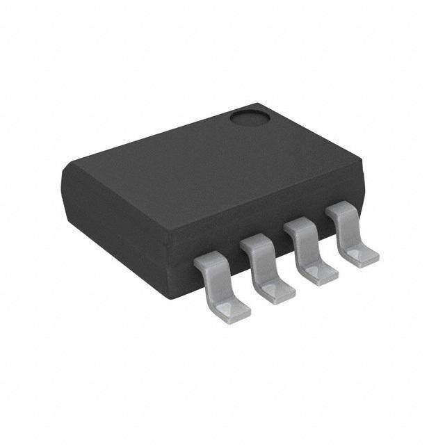
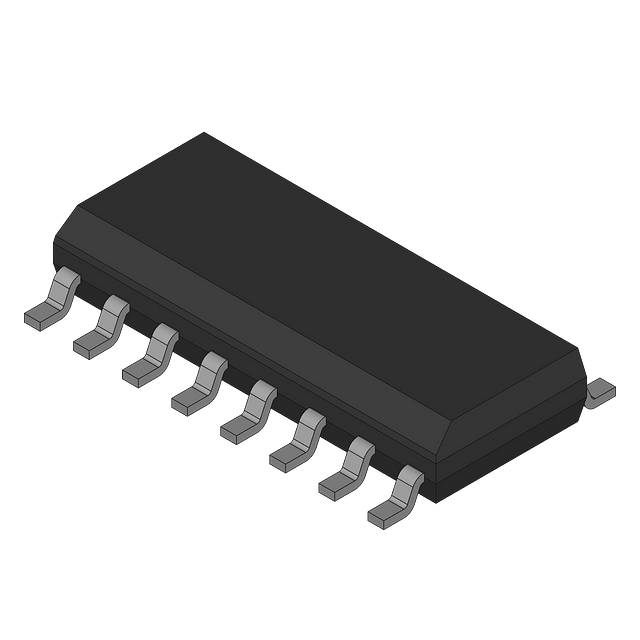
| 描述 | IC ASK RCVR RF/IF SHUTDWN 16SOIC射频接收器 300-440MHz RF Receiver With Shutdown( Lead Free) |
| 产品分类 | |
| 品牌 | Micrel |
| 产品手册 | |
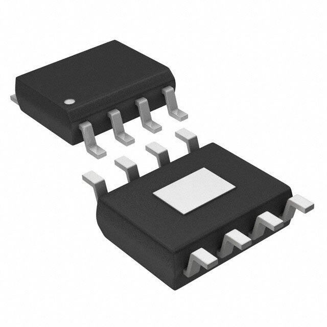
| 产品图片 |
|
| rohs | 符合RoHS无铅 / 符合限制有害物质指令(RoHS)规范要求 |
| 产品系列 | RF集成电路,射频接收器,Micrel MICRF002YMQwikRadio® |
| 数据手册 | |
| 产品型号 | MICRF002YM |
| 产品目录页面 | |
| 产品种类 | 射频接收器 |
| 供应商器件封装 | 16-SOIC |
| 其它名称 | 576-1332 |
| 包装 | 管件 |
| 商标 | Micrel |
| 天线连接器 | PCB,表面贴装 |
| 存储容量 | - |
| 安装风格 | SMD/SMT |
| 封装 | Tube |
| 封装/外壳 | 16-SOIC(0.154",3.90mm 宽) |
| 封装/箱体 | SOIC-16 |
| 工作温度 | -40°C ~ 85°C |
| 工作电源电压 | 4.75 V to 5.5 V |
| 工作频率 | 300 MHz to 440 MHz |
| 工厂包装数量 | 48 |
| 应用 | RKE |
| 数据接口 | PCB,表面贴装 |
| 数据速率(最大值) | 10 kbps |
| 最大工作温度 | + 85 C |
| 最小工作温度 | - 40 C |
| 标准包装 | 48 |
| 灵敏度 | -95dBm |
| 特性 | 自动调谐 |
| 电压-电源 | 4.75 V ~ 5.5 V |
| 电流-接收 | 2.2mA |
| 电源电压-最大 | 5.5 V |
| 电源电压-最小 | 4.75 V |
| 电源电流 | 2.2 mA |
| 类型 | ASK Receiver |
| 系列 | MICRF022 |
| 调制或协议 | ASK,OOK |
| 频率 | 300MHz ~ 440MHz |



- 商务部:美国ITC正式对集成电路等产品启动337调查
- 曝三星4nm工艺存在良率问题 高通将骁龙8 Gen1或转产台积电
- 太阳诱电将投资9.5亿元在常州建新厂生产MLCC 预计2023年完工
- 英特尔发布欧洲新工厂建设计划 深化IDM 2.0 战略
- 台积电先进制程称霸业界 有大客户加持明年业绩稳了
- 达到5530亿美元!SIA预计今年全球半导体销售额将创下新高
- 英特尔拟将自动驾驶子公司Mobileye上市 估值或超500亿美元
- 三星加码芯片和SET,合并消费电子和移动部门,撤换高东真等 CEO
- 三星电子宣布重大人事变动 还合并消费电子和移动部门
- 海关总署:前11个月进口集成电路产品价值2.52万亿元 增长14.8%


.jpg)


PDF Datasheet 数据手册内容提取
MICRF002/RF022 Micrel MICRF002/RF022 300-440MHz QwikRadio™ASK Receiver Final Information General Description The MICRF002 is a single chip ASK/OOK (ON-OFF Keyed) RF receiver IC. This device is a true “antenna-in to data-out” monolithic device. All RF and IF tuning is accomplished QwikRadio™ automatically within the IC which eliminates manual tuning and reduces production costs. The result is a highly reliable Features yet low cost solution. The MICRF002 is a fully featured part in 16-pin packaging, • 300MHz to 440MHz frequency range the MICRF022 is the same part packaged in 8-pin packaging • Data-rate up to 10kbps (fixed-mode) with a reduced feature set (see “Ordering Information” for • Low Power Consumption more information). • 2.2mA fully operational (315MHz) • 0.9µA in shutdown The MICRF002 is an enhanced version of the MICRF001 • 220µA in polled operation (10:1 duty-cycle) and MICRF011. The MICRF002 provides two additional • Wake-up output flag to enable decoders and micropro- functions over the MICRF001/011, (1) a Shutdown pin, which cessors may be used to turn the device off for duty-cycled operation, • Very low RF reradiation at the antenna and (2) a “Wake-up” output, which provides an output flag • Highly integrated with extremely low external part count indicating when an RF signal is present. These features make the MICRF002 ideal for low and ultra-low power applications, such as RKE and remote controls. Applications All IF filtering and post-detection (demodulator) data filtering • Automotive Remote Keyless Entry (RKE) is provided within the MICRF002, so no external filters are • Remote controls necessary. One of four demodulator filter bandwidths may be • Remote fan and light control selected externally by the user. • Garage door and gate openers The MICRF002 offer two modes of operation; fixed-mode (FIX) and sweep-mode (SWP). In fixed mode the MICRF002 functions as a conventional superhet receiver. In sweep mode the MICRF002 employs a patented sweeping function to sweep a wider RF spectrum. Fixed-mode provides better selectivity and sensitivity performance and sweep mode enables the MICRF002 to be used with low cost, imprecise transmitters. Typical Application 1/4 Wave Monopole MICRF002 SSEELL00 SWEN 12pF VSSRF REFOSC 4.8970MHz 68nH VSSRF SEL1 ANT CAGC +5V VDDRF WAKEB 4.7uF VDDBB SHUT Data CTH DO Output 12nH 0.047uF NC VSSBB 315MHz 800bps On-Off Keyed Receiver QwikRadio is a trademark of Micrel, Inc. The QwikRadio ICs were developed under a partnership agreement with AIT of Orlando, Florida. Micrel, Inc. • 1849 Fortune Drive • San Jose, CA 95131 • USA • tel + 1 (408) 944-0800 • fax + 1 (408) 944-0970 • http://www.micrel.com March 2003 1 MICRF002/RF022
MICRF002/RF022 Micrel Ordering Information Demodulator WAKEB Part Number Bandwidth Operating Mode Shutdown Output Flag Package MICRF002BM User Programable Fixed or Sweep Yes Yes 16-Pin SOP MICRF022BM-SW48 5000Hz Sweep No Yes 8-Pin SOP MICRF022BM-FS12 1250Hz Fixed Yes No 8-Pin SOP MICRF022BM-FS24 2500Hz Fixed Yes No 8-Pin SOP MICRF022BM-FS48 5000Hz Fixed Yes No 8-Pin SOP Pin Configuration MICRF002Bx SEL0 1 16 SWEN SEL0 VSSRF 2 15 REFOSC MICRF022Bx-xxxx VSSRF 3 14 SEL1 VSSRF 1 8 REFOSC ANT 4 13 CAGC ANT 2 7 CAGC VDDRF 5 12 WAKEB VDDRF 3 6 SHUT/WAKEB VDDBB 6 11 SHUT CTH 4 5 DO CTH 7 10 DO NC 8 9 VSSBB Standard 16-Pin or 8-Pin SOP (M) Packages 8-Pin Options The standard 16-pin package allows complete control of all configurable features. Some reduced function 8-pin versions are also available, see “Ordering Information” above. For high-volume applications additional customized 8-pin devices can be produced. SWEN, SEL0 and SEL1 pins are internally bonded to reduce the pin count. pin 6 may be configured as either SHUT or WAKEB. DemodulatorBandwidth SEL0 SEL1 SweepMode FIXEDMode 1 1 5000Hz 10000Hz 0 1 2500Hz 5000Hz 1 0 1250Hz 2500Hz 0 0 625Hz 1250Hz Table 1. Nominal Demodulator Filter Bandwidth vs. SEL0, SEL1 and Operating Mode MICRF002/RF022 2 March 2003
MICRF002/RF022 Micrel Pin Description Pin Number Pin Number Pin Name Pin Function 16-Pin Pkg. 8-Pin Pkg. 1 SEL0 Bandwidth Selection Bit 0 (Digital Input): Used in conjunction with SEL1 to set the desired demodulator filter bandwidth. See Table 1. Internally pulled- up to VDDRF 2, 3 1 VSSRF RF Power Supply: Ground return to the RF section power supply. 4 2 ANT Antenna (Analog Input): For optimal performance the ANT pin should be impedance matched to the antenna. See “Applications Information” for information on input impedance and matching techniques 5 3 VDDRF RF Power Supply: Positive supply input for the RF section of the IC 6 VDDBB Base-Band Power Supply: Positive supply input for the baseband section (digital section) of the IC 7 4 CTH Data Slicing Threshold Capacitor (Analog I/O): Capacitor connected to this pin extracts the dc average value from the demodulated waveform which becomes the reference for the internal data slicing comparator 8 NC Not internally connected 9 VSSBB Base-Band Power Supply: Ground return to the baseband section power supply 10 5 DO Data Output (Digital Output) 11 6 SHUT Shutdown (Digital Input): Shutdown-mode logic-level control input. Pull low to enable the receiver. Internally pulled-up to VDDRF 12 WAKEB Wakeup (Digital Output): Active-low output that indicates detection of an incoming RF signal 13 7 CAGC Automatic Gain Control (Analog I/O): Connect an external capacitor to set the attack/decay rate of the on-chip automatic gain control 14 SEL1 Bandwidth Selection Bit 1 (Digital Input): Used in conjunction with SEL0 to set the desired demodulator filter bandwidth. See Table 1. Internally pulled- up to VDDRF 15 8 REFOSC Reference Oscillator: Timing reference, sets the RF receive frequency. 16 SWEN Sweep-Mode Enable (Digital Input): Sweep- or Fixed-mode operation control input. SWEN high= sweep mode; SWEN low = conventional superheterodyne receiver. Internally pulled-up to VDDRF March 2003 3 MICRF002/RF022
MICRF002/RF022 Micrel Absolute Maximum Ratings (Note 1) Operating Ratings (Note 2) Supply Voltage (V , V )....................................+7V Supply Voltage (V , V )................+4.75V to +5.5V DDRF DDBB DDRF DDBB Input/Output Voltage (V ) .................V –0.3 to V +0.3 RF Frequency Range............................. 300MHz to 440Hz I/O SS DD Junction Temperature (T )......................................+150°C Data Duty-Cycle...............................................20% to 80% J Storage Temperature Range (T )............–65°C to +150°C Reference Oscillator Input Range............0.1V to 1.5V S PP PP Lead Temperature (soldering, 10 sec.)...................+260°C Ambient Temperature (T ).........................–40°C to +85°C A ESD Rating, Note 3 Electrical Characteristics V = V = V where +4.75V ≤ V ≤ 5.5V, V = 0V; C = 4.7µF, C = 100nF; SEL0 = SEL1 = V ; fixed mode ( SWEN DDRF DDBB DD DD SS AGC TH SS = V ); f = 4.8970MHz (equivalent to f = 315MHz); data-rate = 1kbps (Manchester encoded). T = 25°C, bold values indicate SS REFOSC RF A –40°C ≤ T ≤ +85°C; current flow into device pins is positive; unless noted. A Symbol Parameter Condition Min Typ Max Units I Operating Current continuous operation, f = 315MHz 2.2 3.2 mA OP RF polled with 10:1 duty cycle, f = 315MHz 220 µA RF continuous operation, f = 433.92MHz 3.5 mA RF polled with 10:1 duty cycle, f = 433.92MHz 350 µA RF I Standby Current V = V 0.9 µA STBY SHUT DD RF Section, IF Section Receiver Sensitivity (Note 4) f = 315MHz –97 dBm RF f = 433.92MHz –95 dBm RF f IF Center Frequency Note 6 0.86 MHz IF f IF Bandwidth Note 6 0.43 MHz BW Maximum Receiver Input R = 50Ω –20 dBm SC Spurious Reverse Isolation ANT pin, R = 50Ω, Note 5 30 µVrms SC AGC Attack to Decay Ratio t ÷ t 0.1 ATTACK DECAY AGC Leakage Current T = +85°C ±100 nA A Reference Oscillator Z Reference Oscillator Note 8 290 kΩ REFOSC Input Impedance Reference Oscillator Source 5.2 uA Current Demodulator Z CTH Source Impedance Note 7 145 kΩ CTH I CTH Leakage Current T = +85°C ±100 nA ZCTH(leak) A Demodulator Filter Bandwidth V = V .V = V 4000 Hz SEL0 DD SEL1 DD Sweep Mode V = V . V = V 2000 Hz SEL0 SS SEL1 DD (SWEN = V or OPEN) V = V .V = V 1000 Hz DD SEL0 DD SEL1 SS Note 6 V = V . V = V 500 Hz SEL0 SS SEL1 SS Demodulator Filter Bandwidth V = V .V = V 8000 Hz SEL0 DD SEL1 DD Fixed Mode V = V . V = V 4000 Hz SEL0 SS SEL1 DD (SWEN = V V = V .V = V 2000 Hz SS SEL0 DD SEL1 SS Note 6 V = V . V = V 1000 Hz SEL0 SS SEL1 SS MICRF002/RF022 4 March 2003
MICRF002/RF022 Micrel Symbol Parameter Condition Min Typ Max Units Digital/Control Section V Input-High Voltage SEL0, SEL1, SWEN 0.8 V IN(high) DD V Input-Low Voltage SEL0, SEL1, SWEN 0.2 V IN(low) DD I Output Current DO, WAKEB pins, push-pull 10 µA OUT V Output High Voltage DO, WAKEB pins, I = –1µA 0.9 V OUT(high) OUT DD V Output Low Voltage DO, WAKEB pins, I = +1µA 0.1 V OUT(low) OUT DD t , t Output Rise and Fall Times DO, WAKEB pins, C = 15pF 10 µs R F LOAD Note 1. Exceeding the absolute maximum rating may damage the device. Note 2. The device is not guaranteed to function outside its operating rating. Note 3. Devices are ESD sensitive, use appropriate ESD precautions. Meets class 1 ESD test requirements, (human body model HBM), in accor- dance with MIL-STD-883C, method 3015. Do not operate or store near strong electrostatic fields. Note 4: Sensitivity is defined as the average signal level measured at the input necessary to achieve 10-2 BER (bit error rate). The RF input is assumed to be matched to 50Ω. Note 5: Spurious reverse isolation represents the spurious components which appear on the RF input pin (ANT) measured into 50Ω with an input RF matching network. Note 6: Parameter scales linearly with reference oscillator frequency f . For any reference oscillator frequency other than 4.8970MHz, compute T new parameter value as the ratio: f MHz REFOSC ×(parameter value at 4.8970MHz) 4.8970MHz Note 7: Parameter scales inversely with reference oscillator frequency f . For any reference oscillator frequency other than 4.8970MHz, compute T new parameter value as the ratio: 4.8970MHz ×(parameter value at 4.8970MHz) f MHz REFOSC Note 8: Series resistance of the resonator (ceramic resonator or crystal) should be minimized to the extent possible. In cases where the resonator series resistance is too great, the oscillator may oscillate at a diminished peak-to-peak level, or may fail to oscillate entirely. Micrel recom- mends that series resistances for ceramic resonators and crystals not exceed 50Ohms and 100Ohms respectively. Refer to Application Hint 35 for crystal recommendations. March 2003 5 MICRF002/RF022
MICRF002/RF022 Micrel Typical Characteristics Supply Current Supply Current vs. Frequency vs. Temperature 3.5 6.0 T = 25°C f = 315MHz A VDD = 5V 3.0 VDD = 5V NT (mA)4.5 ENT (mA)2.5 E R R R CUR3.0 CU2.0 Sweep Mode, Sweep Mode, Continuous Operation Continuous Operation 1.5 1.5 -40 -20 0 20 40 60 80 100 250 300 350 400 450 500 TEMPERATURE (°C) FREQUENCY (MHz) MICRF002/RF022 6 March 2003
MICRF002/RF022 Micrel Functional Diagram CAGC AGC Control CAGC 5th Order Pr2ongrda Omrmdearble SCwapitcahceitodr- Band-Pass Filter Low-Pass Filter Resistor ANT RF fRX fIF IF IF Peak Amp Amp Amp Detector DO R Compa- SC rator f 430kHz LO VDD CTH Programmable VSS Synthesizer C UHF Downconverter OOK Demodulator TH SEL0 SEL1 Control WAKEB SWEN Logic Resettable Counter SHUT REFOSC fT Reference Reference and Control Wakeup Cystal Oscillator or Ceramic Resonator MICRF002 Figure 1. MICRF002 Block Diagram Applications Information and Functional Step 1: Selecting The Operating Mode Description Fixed-Mode Operation Refer to figure 1 “MICRF002 Block Diagram”. Identified in the For applications where the transmit frequency is accurately block diagram are the four sections of the IC: UHF set (that is, applications where a SAW or crystal-based Downconverter, OOK Demodulator, Reference and Control, transmitter is used) the MICRF002 may be configured as a and Wakeup. Also shown in the figure are two capacitors standard superheterodyne receiver (fixed mode). In fixed- (C , C ) and one timing component, usually a crystal or mode operation the RF bandwidth is narrower making the TH AGC ceramic resonator. With the exception of a supply decoupling receiver less susceptible to interfering signals. Fixed mode is capacitor, and antenna impedance matching network, these selected by connecting SWEN to ground. are the only external components needed by the MICRF002 Sweep-Mode Operation to assemble a complete UHF receiver. When used in conjunction with low-cost L-C transmitters the For optimal performance is highly recommended that the MICRF002 should be configured in sweep-mode. In sweep- MICRF002 is impedance matched to the antenna, the match- mode, while the topology is still superheterodyne, the LO ing network will add an additional two or three components. (local oscillator) is swept over a range of frequencies at rates Four control inputs are shown in the block diagram: SEL0, greater than the data rate. This technique effectively in- SEL1, SWEN, and SHUT. Using these logic inputs, the user creases the RF bandwidth of the MICRF002, allowing the can control the operating mode and selectable features of the device to operate in applications where significant transmit- IC. These inputs are CMOS compatible, and are internally ter-receiver frequency misalignment may exist. The transmit pulled-up. IF Bandpass Filter Roll-off response of the IF Filter frequency may vary up to ±0.5% over initial tolerance, aging, is 5th order, while the demodulator data filter exhibits a 2nd and temperature. In sweep-mode a band approximately order response. 1.5% around the nominal transmit frequency is captured. The transmitter may drift up to ±0.5% without the need to retune the receiver and without impacting system performance. Design Steps The swept-LO technique does not affect the IF bandwidth, The following steps are the basic design steps for using the therefore noise performance is not degraded relative to fixed MICRF002 receiver: mode. The IF bandwidth is 430kHz whether the device is operating in fixed or sweep-mode. 1). Select the operating mode (sweep or fixed) Due to limitations imposed by the LO sweeping process, the 2). Select the reference oscillator upper limit on data rate in sweep mode is approximately 3). Select the C capacitor TH 5.0kbps. 4). Select the C capacitor AGC Similar performance is not currently available with crystal- 5). Select the demodulator filter bandwidth based superheterodyne receivers which can operate only with SAW- or crystal-based transmitters. March 2003 7 MICRF002/RF022
MICRF002/RF022 Micrel In sweep-mode, a range reduction will occur in installations Frequency f is in MHz. Connect a crystal of frequency f to T T where there is a strong interferer in the swept RF band. This REFOSC on the MICRF002. Four-decimal-place accuracy is because the process indiscriminately includes all signals on the frequency is generally adequate. The following table within the sweep range. An MICRF002 may be used in place identifies f for some common transmit frequencies when the T of a superregenerative receiver in most applications. MICRF002 is operated in fixed mode. Step 2: Selecting The Reference Oscillator Transmit ReferenceOscillator Frequency Frequency All timing and tuning operations on the MICRF002 are de- f f TX T rived from the internal Colpitts reference oscillator. Timing 315MHz 4.8970MHz and tuning is controlled through the REFOSC pin in one of 390MHz 6.0630MHz three ways: 418MHz 6.4983MHz 1. Connect a ceramic resonator 433.92MHz 6.7458MHz 2. Connect a crystal Table 2. Fixed Mode Recommended Reference 3. Drive this pin with an external timing signal Oscillator Values For Typical Transmit Frequencies The specific reference frequency required is related to the (high-side mixing) system transmit frequency and to the operating mode of the receiver as set by the SWEN pin. Selecting REFOSC Frequency f T (Sweep Mode) Crystal or Ceramic Resonator Selection Selection of the reference oscillator frequency f in sweep Do not use resonators with integral capacitors since capaci- T mode is much simpler than in fixed mode due to the LO tors are included in the IC, also care should be taken to sweeping process. Also, accuracy requirements of the fre- ensure low ESR capacitors are selected. Application Hint 34 quency reference component are significantly relaxed. and Application Hint 35 provide additional information and recommended sources for crystals and resonators. In sweep mode, f is given by Equation 3: T If operating in fixed-mode, a crystal is recommended. In f sweep-mode either a crystal or ceramic resonator may be (3) fT = 64L.O25 used. When a crystal of ceramic resonator is used the In SWEEP mode a reference oscillator with frequency accu- minimum voltage is 300mV . If using an externally applied PP rate to two-decimal-places is generally adequate. A crystal signal it should be AC-coupled and limited to the operating may be used and may be necessary in some cases if the range of 0.1V to 1.5V PP PP. transmit frequency is particularly imprecise. Selecting Reference Oscillator Frequency f T (Fixed Mode) Transmit ReferenceOscillator Frequency Frequency As with any superheterodyne receiver, the mixing between f f the internal LO (local oscillator) frequency f and the incom- TX T LO 315MHz 4.88MHz ing transmit frequency f ideally must equal the IF center TX 390MHz 6.05MHz frequency. Equation 1 may be used to compute the appropri- ate f for a given f : 418MHz 6.48MHz LO TX 433.92MHz 6.73MHz f (1) fLO = fTX ±0.863T1X5 Table 3. Recommended Reference Oscillator Values For Typical Transmit Frequencies (sweep-mode) Frequencies f and f are in MHz. Note that two values of TX LO f exist for any given f , distinguished as “high-side mixing” LO TX and “low-side mixing.” High-side mixing results in an image frequency above the frequency of interest and low-side mixing results in a frequency below. After choosing one of the two acceptable values of f , use LO Equation 2 to compute the reference oscillator frequency f : T f (2) f = LO T 64.5 MICRF002/RF022 8 March 2003
MICRF002/RF022 Micrel Step 3: Selecting The C Capacitor Selecting C Capacitor in Continuous Mode TH AGC A C capacitor in the range of 0.47µF to 4.7µF is typically Extraction of the dc value of the demodulated signal for AGC recommended. The value of the C should be selected to purposes of logic-level data slicing is accomplished using the AGC minimize the ripple on the AGC control voltage by using a external threshold capacitor C and the on-chip switched- TH sufficiently large capacitor. However if the capacitor is too capacitor “resistor” R , shown in the block diagram. SC large the AGC may react too slowly to incoming signals. AGC Slicing level time constant values vary somewhat with de- settling time from a completely discharged (zero-volt) state is coder type, data pattern, and data rate, but typically values given approximately by Equation 6: range from 5ms to 50ms. Optimization of the value of C is TH required to maximize range. (6) ∆t=1.333C −0.44 AGC Selecting Capacitor C where: TH The first step in the process is selection of a data-slicing-level C is in µF, and ∆t is in seconds. AGC time constant. This selection is strongly dependent on sys- Selecting C Capacitor in Duty-Cycle Mode tem issues including system decode response time and data AGC Voltage droop across the C capacitor during shutdown code structure (that is, existence of data preamble, etc.). This AGC should be replenished as quickly as possible after the IC is issue is covered in more detail in Application Note 22. enabled. As mentioned above, the MICRF002 boosts the The effective resistance of R is listed in the electrical SC push-pull current by a factor of 45 immediately after start-up. characteristics table as 145kΩ at 315MHz, this value scales This fixed time period is based on the reference oscillator linearly with frequency. Source impedance of the CTH pin at frequency f . The time is 10.9ms for f = 6.00MHz, and varies other frequencies is given by equation (4), where f is in MHz: T T T inversely with f . The value of C capacitor and the T AGC 4.8970 duration of the shutdown time period should be selected such (4) RSC =145kΩ f that the droop can be replenished within this 10ms period. T Polarity of the droop is unknown, meaning the AGC voltage τ of 5x the bit-rate is recommended. Assuming that a slicing could droop up or down. Worst-case from a recovery stand- level time constant τ has been established, capacitor C TH point is downward droop, since the AGC pull-up current is may be computed using equation 1/10th magnitude of the pulldown current. The downward τ droop is replenished according to the Equation 7: C = (5) TH RSC I = ∆V A standard ±20% X7R ceramic capacitor is generally suffi- (7) CAGC ∆t cient. Refer to Application Hint 42 for C and C selection TH AGC where: examples. I = AGC pullup current for the initial 10ms (67.5µA) Step 4: Selecting The C Capacitor C = AGC capacitor value AGC AGC The signal path has AGC (automatic gain control) to increase ∆t = droop recovery time input dynamic range. The attack time constant of the AGC is ∆V = droop voltage set externally by the value of the CAGC capacitor connected For example, if user desires ∆t = 10ms and chooses a 4.7µF to the CAGC pin of the device. To maximize system range, it C , then the allowable droop is about 144mV. Using the is important to keep the AGC control voltage ripple low, AGC same equation with 200nA worst case pin leakage and preferably under 10mVpp once the control voltage has at- assuming 1µA of capacitor leakage in the same direction, the tained its quiescent value. For this reason capacitor values of maximum allowable ∆t (shutdown time) is about 0.56s for at least 0.47µF are recommended. droop recovery in 10ms. The AGC control voltage is carefully managed on-chip to The ratio of decay-to-attack time-constant is fixed at 10:1 allow duty-cycle operation of the MICRF002. When the (that is, the attack time constant is 1/10th of the decay time device is placed into shutdown mode (SHUT pin pulled high), constant). Generally the design value of 10:1 is adequate for the AGC capacitor floats to retain the voltage. When opera- the vast majority of applications. If adjustment is required the tion is resumed, only the voltage droop due to capacitor constant may be varied by adding a resistor in parallel with the leakage must be replenished. A relatively low-leakage ca- C capacitor. The value of the resistor must be determined pacitor is recommended when the devices are used in duty- AGC on a case by case basis. cycled operation. Step 5: Selecting The Demod Filter To further enhance duty-cycled operation, the AGC push and pull currents are boosted for approximately 10ms immedi- Bandwidth ately after the device is taken out of shutdown. This compen- The inputs SEL0 and SEL1 control the demodulator filter sates for AGC capacitor voltage droop and reduces the time bandwidth in four binary steps (625Hz to 5000Hz in sweep, to restore the correct AGC voltage. The current is boosted by 1250Hz to 10000Hz in fixed mode), see Table 1. Bandwidth a factor of 45. must be selected according to the application. The demodu- lator bandwidth should be set according to equation 8. March 2003 9 MICRF002/RF022
MICRF002/RF022 Micrel (8) Demoulator bandwidth = 0.65 / Shortest pulse-width It should be noted that the values indicated in table 1 are nominal values. The filter bandwidth scales linearly with frequency so the exact value will depend on the operating frequency. Refer to the “Electrical Characteristics” for the exact filter bandwidthat a chosen frequency. DemodulatorBandwidth SEL0 SEL1 SweepMode FIXEDMode 1 1 5000Hz 10000Hz 0 1 2500Hz 5000Hz 1 0 1250Hz 2500Hz 0 0 625Hz 1250Hz Table 1. Nominal Demodulator Filter Bandwidth vs. SEL0, SEL1 and Operating Mode MICRF002/RF022 10 March 2003
MICRF002/RF022 Micrel Additional Applications Information Frequency Z ( ) IN S11 L (nH) L (nH) In addition to the basic operation of the MICRF002 the (MHz) Z11 SHUNT SERIES following enhancements can be made. In particilar it is 300 12– j166 0.803– j0.529 15 72 strongly recommended that the antenna impedance is 305 12– j165 0.800– j0.530 15 72 matched to the input of the IC. 310 12– j163 0.796– j0.536 15 72 Antenna Impedance Matching As shown in table 4 the antenna pin input impedance is 315 13– j162 0.791– j0.536 15 72 frequency dependant. 320 12– j160 0.789– j0.543 15 68 The ANT pin can be matched to 50 Ohms with an L-type 325 12– j157 0.782– j0.550 12 68 circuit. That is, a shunt inductor from the RF input to ground 330 12-j155 0.778– j0.556 12 68 and another in series from the RF input to the antenna pin. Inductor values may be different from table depending on 335 12– j152 0.770– j0.564 12 68 PCB material, PCB thickness, ground configuration, and how 340 11-j150 0.767– j0.572 15 56 long the traces are in the layout. Values shown were charac- 345 11– j148 0.762– j0.578 15 56 terized for a 0.031 thickness, FR4 board, solid ground plane on bottom layer, and very short traces. MuRata and Coilcraft 350 11– j145 0.753– j0.586 12 56 wire wound 0603 or 0805 surface mount inductors were 355 11– j143 0.748– j0.592 12 56 tested, however any wire wound inductor with high SRF (self 360 11– j141 0.742– j0.597 10 56 resonance frequency) should do the job. 365 11– j139 0.735– j0.603 10 56 Shutdown Function Duty-cycled operation of the MICRF002 (often referred to as 370 10– 137 0.732– j0.612 12 47 polling) is achieved by turning the MICRF002 on and off via 375 10– j135 0.725– j0.619 12 47 the SHUT pin. The shutdown function is controlled by a logic 380 10– j133 0.718– j0.625 10 47 state applied to the SHUT pin. When V is high, the SHUT device goes into low-power standby mode. This pin is pulled 385 10– j131 0.711– j0.631 10 47 high internally, it must be externally pulled low to enable the 390 10– j130 0.707– j0.634 10 43 receiver. 395 10– j128 0.700– j0.641 10 43 400 10– j126 0.692– j0.647 10 43 405 10– j124 0.684– j0.653 10 39 410 10– j122 0.675– j0.660 10 39 L SERIES 415 10– j120 0.667– j0.667 10 39 420 10– j118 0.658– j0.673 10 36 L SHUNT 425 10– j117 0.653– j0.677 10 36 430 10– j115 0.643– j0.684 10 33 435 10– j114 0.638– j0.687 10 33 440 8– j112 0.635– j0.704 8.2 33 Table 4. Input Impedance Versus Frequency j25 j100 ∞ 0 50 –j25 –j100 March 2003 11 MICRF002/RF022
MICRF002/RF022 Micrel Power Supply Bypass Capacitors where: VDDBB and VDDRF should be connected together directly at f = reference oscillator frequency T the IC pins. Supply bypass capacitors are strongly f = system clock frequency S recommended. They should be connected to VDDBB and P = system clock period VDDRF and should have the shortest possible lead lengths. S For best performance, connect VSSRF to VSSBB at the The Wake-Up counter will reset immediately after a detected power supply only (that is, keep V currents from flowing RF carrier drops. The duration of the Wake-Up signal output SSBB through the V return path). is then determined by the required wake up time plus an SSRF additional RF carrier on time interval to create a wake up Increasing Selectivity With an Optional BandPass pulse output. Filter WAKEB Output Pulse Time = T + Additional RF For applications located in high ambient noise environments, WAKE Carrier On Time a fixed value band-pass network may be connected between For designers who wish to use the wakeup function while the ANT pin and VSSRF to provide additional receive selec- squelching the output, a positive squelching offset voltage tivity and input overload protection. A minimum input configu- must be used. This simply requires that the squelch resistor ration is included in figure 7a. it provides some filtering and be connected to a voltage more positive than the quiescent necessary overload protection. voltage on the CTH pin so that the data output is low in Data Squelching absence of a transmission. During quiet periods (no signal) the data output (DO pin) I/O Pin Interface Circuitry transitions randomly with noise. Most decoders can descriminate between this random noise and actual data but Interface circuitry for the various I/O pins of the MICRF002 for some system it does present a problem. There are three are diagrammed in Figures 1 through 6. The ESD protection possible approaches to reducing this output noise: diodes at all input and output pins are not shown. 1). Analog squelch to raise the demodulator threshold 2). Digital squelch to disable the output when data is not CTH Pin present VDDBB 3). Output filter to filter the (high frequency) noise glitches on the data output pin. PHI2B PHI1B Demodulator The simplest solution is add analog squelch by introducing a Signal small offset, or squelch voltage, on the CTH pin so that noise 2.85Vdc CTH does not trigger the internal comparator. Usually 20mV to 30mV is sufficient, and may be achieved by connecting a 6.9pF PHI2 PHI1 several-megohm resistor from the CTH pin to either V or VSSBB VSSBB SS V , depending on the desired offset polarity. Since the DD Figure 2. CTH Pin MICRF002 has receiver AGC noise at the internal compara- tor input is always the same, set by the AGC. The squelch Figure 2 illustrates the CTH-pin interface circuit. The CTH pin offset requirement does not change as the local noise strength is driven from a P-channel MOSFET source-follower with changes from installation to installation. Introducing squelch approximately 10µA of bias. Transmission gates TG1 and will reduce sensitivity and also reduce range. Only introduce TG2 isolate the 6.9pF capacitor. Internal control signals an amount of offset sufficient to quiet the output. Typical PHI1/PHI2 are related in a manner such that the impedance squelch resistor values range from 6.8MΩ to 10MΩ. across the transmission gates looks like a “resistance” of Wake-Up Function approximately 100kΩ. The dc potential at the CTH pin is approximately 1.6V The WAKEB output signal can be used to reduce system power consumption by enabling the rest of a system when an RF signal is present. The WAKEB is an output logic signal which goes active low when the IC detects a constant RF carrier. The wake-up function is unavailable when the IC is in shutdown mode. To activate the Wake-Up function, a received constant RF carrier must be present for 128 counts or the internal system clock. The internal system clock is derived from the reference oscillator and is 1/256 the reference oscillator frequency. For example: f = 6.4MHz T f = f /256 = 25kHz S T P = 1/f = 0.04ms S S 128 counts x 0.04ms = 5.12ms MICRF002/RF022 12 March 2003
MICRF002/RF022 Micrel CAGC Pin REFOSC Pin VDDBB VDDBB Active Bias 200k 1.5µA 67.5µA REFOSC Compa- 30pF 250Ω rator 30pF 30µA CAGC VSSBB VSSBB Timout Figure 5. REFOSC Pin 15µA 675µA The REFOSC input circuit is shown in Figure 5. Input imped- ance is high (200kΩ). This is a Colpitts oscillator with internal VSSBB 30pF capacitors. This input is intended to work with standard Figure 3. CAGC Pin ceramic resonators connected from this pin to the VSSBB pin, although a crystal may be used when greater frequency accuracy is required. The nominal dc bias voltage on this pin Figure 3 illustrates the CAGC pin interface circuit. The AGC is 1.4V. control voltage is developed as an integrated current into a SEL0, SEL1, SWEN, and SHUT Pins capacitor C . The attack current is nominally 15µA, while the decay cuArGreCnt is a 1/10th scaling of this, nominally 1.5µA, VDDBB making the attack/decay time constant ratio a fixed 10:1. Signal gain of the RF/IF strip inside the IC diminishes as the Q1 voltage at CAGC decreases. Modification of the attack/decay Q2 VSSBB ratio is possible by adding resistance from the CAGC pin to to Internal either V or V , as desired. SHUT Q4 Circuits DDBB SSBB SEL0, Q3 Both the push and pull current sources are disabled during SEL1, SWEN shutdown, which maintains the voltage across C , and AGC VSSBB improves recovery time in duty-cycled applications. To fur- ther improve duty-cycle recovery, both push and pull currents Figure 6a. SEL0, SEL1, SWEN are increased by 45 times for approximately 10ms after VDDBB release of the SHUT pin. This allows rapid recovery of any voltage droop on C while in shutdown. AGC DO and WAKEB Pins Q1 Q2 to Internal VDDBB VSSBB Circuits 10µA SHUT Q3 Compa- VSSBB rator DO Figure 6b. SHUT Control input circuitry is shown in Figures 6a and 6b. The standard input is a logic inverter constructed with minimum geometry MOSFETs (Q2, Q3). P-channel MOSFET Q1 is a 10µA large channel length device which functions essentially as a VSSBB “weak” pullup to VDDBB. Typical pullup current is 5µA, leading to an impedance to the VDDBB supply of typically Figure 4. DO and WAKEB Pins 1MΩ. The output stage for DO (digital output) and WAKEB (wakeup output) is shown in Figure 4. The output is a 10µA push and 10µA pull switched-current stage. This output stage is ca- pable of driving CMOS loads. An external buffer-driver is recommended for driving high-capacitance loads. March 2003 13 MICRF002/RF022
MICRF002/RF022 Micrel Applications Example 315MHz Receiver/Decoder Application Figure 7a illustrates a typical application for the MICRF002 UHF Receiver IC. This receiver operates continuously (not duty cycled) in sweep mode, and features 6-bit address decoding and two output code bits. Operation in this example is at 315MHz, and may be custom- ized by selection of the appropriate frequency reference (Y1), and adjustment of the antenna length. The value of C4 would also change if the optional input filter is used. Changes from the 1kb/s data rate may require a change in the value of R1. A bill of materials accompanies the schematic. 0.4 monopole +5V antenna (11.6in) Supply Input C4 U1 MICRF002 4.8970MHz ad6d-rbeitss U2 HT-12D Optional Filter SSEELL00 SWEN Y1 A0 VDD 8.2pF, 16.6nH R2 pcb foil inductor VSSRF REFOSC A1 VT 1in of 30mil trace L1 VSSRF SEL1 A2 OSC1 1k R1 ANT CAGC A3 OSC2 VDDRF WAKEB 4.7µF A4 DIN 68k C1 4.7µF VDDBB SHUT A5 D11 Code Bit 0 CTH DO A6 D10 Code Bit 1 C2 2.2µF NC VSSBB A7 D9 RF Baseband VSS D8 (Analog) (Digital) Ground Ground Figure 7a. 315MHz, 1kbps On-Off Keyed Receiver/Decoder Item PartNumber Manufacturer Description U1 MICRF002 Micrel UHFreceiver U2 HT-12D Holtek logicdecoder CR1 CSA6.00MG Murata 6.00MHzceramicresonator D1 SSF-LX100LID Lumex redLED R1 68k1/4W5% R2 Vishay 1k1/4W5% C1 Vishay 4.7µFdippedtantalumcapacitor C3 Vishay 4.7µFdippedtantalumcapacitor C2 Vishay 2.2µFdippedtantalumcapacitor C4 Vishay 8.2pFCOGceramiccapacitor Figure 7b. Bill of Material Vendor Telephone FAX Vishay (203)268-6261 — Holtek (408)894-9046 (408)894-0838 Lumex (800)278-5666 (847)359-8904 Murata (800)241-6574 (770)436-3030 Figure 7c. Component Vendors MICRF002/RF022 14 March 2003
MICRF002/RF022 Micrel PCB Layout Information The MICRF002 evaluation board was designed and charac- terized using two sided 0.031 inch thick FR4 material with 1 ounce copper clad. If another type of printed circuit board material were to be substituted, impedance matching and characterization data stated in this document may not be valid. The gerber files for this board can be downloaded from the Micrel website at www.micrel.com. PCB Component Side Layout PCB Silk Screen PCB Solder Side Layout J2 C5 REF.OSC. (Not Placed) GND MICRF002 JP1 1 SEL0 SWEN 16 JP3 2 VSSRF REFOSC 15 Y1 6.7458MHz J1 3 VSSRF SEL1 14 JP2 RF INPUT Z1 Z2 4 ANT CAGC 13 C4.47(µCFAGC) 5 VDDRF WAKEB 12 Z3 Z4 6 VDDBB SHUT 11 J5 7 CTH DO 10 SHUT R1 GND 8 N/C VSSBB 9 Squelch R2 Resistor DO 10k (Not Placed) GND J4 J3 C3(CTH) +5V 0.047µF GND C1 C2 4.7µF 0.1µF March 2003 15 MICRF002/RF022
MICRF002/RF022 Micrel Package Information PIN 1 0.157 (3.99) DIMENSIONS: 0.150 (3.81) INCHES (MM) 0.020 (0.51) REF 0.050 (1.27) 0.020 (0.51) BSC 0.013 (0.33) 0.0098 (0.249) 45° 0.0040 (0.102) 0°–8° 0.394 (10.00) 0.050 (1.27) 0.0648 (1.646) 0.386 (9.80) SEATING 0.016 (0.40) 0.0434 (1.102) PLANE 0.244 (6.20) 0.228 (5.79) 16-Pin SOP (M) 0.026 (0.65) MAX) PIN 1 0.157 (3.99) DIMENSIONS: 0.150 (3.81) INCHES (MM) 0.020 (0.51) 0.013 (0.33) 0.050 (1.27) TYP 0.0098 (0.249) 45° 0.010 (0.25) 0.0040 (0.102) 0.007 (0.18) 0.197 (5.0) 0°–8° 0.050 (1.27) 0.064 (1.63) 0.189 (4.8) SEATING 0.016 (0.40) 0.045 (1.14) PLANE 0.244 (6.20) 0.228 (5.79) 8-Pin SOP (M) MICREL, INC. 1849 FORTUNE DRIVE SAN JOSE, CA 95131 USA TEL + 1 (408) 944-0800 FAX + 1 (408) 944-0970 WEB http://www.micrel.com The information furnished by Micrel in this datasheet is believed to be accurate and reliable. However, no responsibility is assumed by Micrel for its use. Micrel reserves the right to change circuitry and specifications at any time without notification to the customer. Micrel Products are not designed or authorized for use as components in life support appliances, devices or systems where malfunction of a product can reasonably be expected to result in personal injury. Life support devices or systems are devices or systems that (a) are intended for surgical implant into the body or (b) support or sustain life, and whose failure to perform can be reasonably expected to result in a significant injury to the user. A Purchaser’s use or sale of Micrel Products for use in life support appliances, devices or systems is at Purchaser’s own risk and Purchaser agrees to fully indemnify Micrel for any damages resulting from such use or sale. © 2003 Micrel, Incorporated. MICRF002/RF022 16 March 2003
Mouser Electronics Authorized Distributor Click to View Pricing, Inventory, Delivery & Lifecycle Information: M icrochip: MICRF022YM-FS48 MICRF022YM-FS48 TR MICRF002YM MICRF022YM-FS24 TR MICRF022YM-FS12 MICRF022YM-FS24 MICRF002YM-TR MICRF022YM-FS12-TR MICRF022YM-FS24-TR MICRF022YM-FS48-TR
 Datasheet下载

