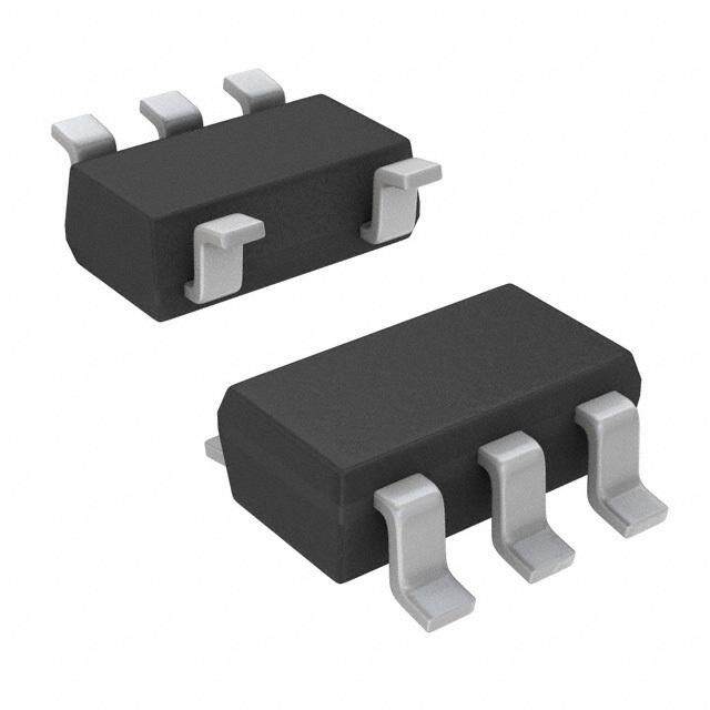
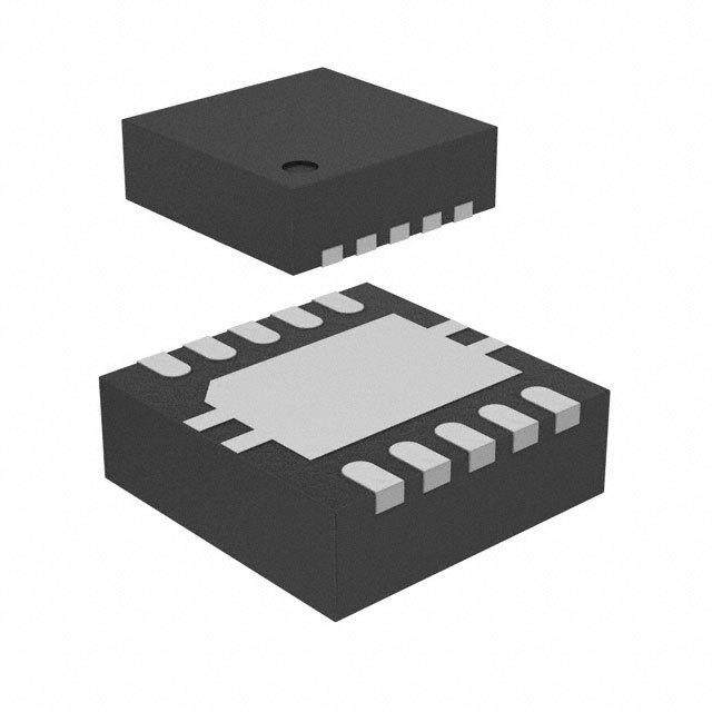
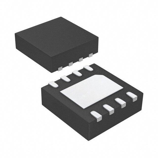
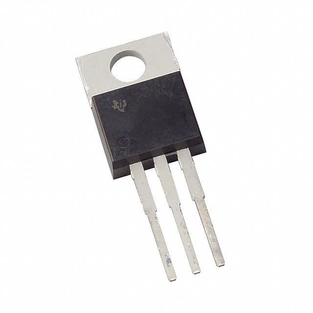
ICGOO在线商城 > 集成电路(IC) > PMIC - 稳压器 - 线性 > MIC5212-SJYM
- 型号: MIC5212-SJYM
- 制造商: Micrel
- 库位|库存: xxxx|xxxx
- 要求:
| 数量阶梯 | 香港交货 | 国内含税 |
| +xxxx | $xxxx | ¥xxxx |
查看当月历史价格
查看今年历史价格
MIC5212-SJYM产品简介:
ICGOO电子元器件商城为您提供MIC5212-SJYM由Micrel设计生产,在icgoo商城现货销售,并且可以通过原厂、代理商等渠道进行代购。 MIC5212-SJYM价格参考。MicrelMIC5212-SJYM封装/规格:PMIC - 稳压器 - 线性, Linear Voltage Regulator IC 正,固定式 2 Output 500mA,500mA 8-SOIC。您可以下载MIC5212-SJYM参考资料、Datasheet数据手册功能说明书,资料中有MIC5212-SJYM 详细功能的应用电路图电压和使用方法及教程。
| 参数 | 数值 |
| 产品目录 | 集成电路 (IC)半导体 |
| 描述 | IC REG LDO 3.3V/2.5V 0.5A 8SOIC低压差稳压器 500mA 1% Low Noise LDO(Lead Free) |
| 产品分类 | |
| 品牌 | Micrel |
| 产品手册 | |
| 产品图片 |
|
| rohs | 符合RoHS无铅 / 符合限制有害物质指令(RoHS)规范要求 |
| 产品系列 | 电源管理 IC,低压差稳压器,Micrel MIC5212-SJYM- |
| 数据手册 | |
| 产品型号 | MIC5212-SJYM |
| 产品目录页面 | |
| 产品种类 | 低压差稳压器 |
| 供应商器件封装 | 8-SOIC |
| 其它名称 | 576-1826-5 |
| 包装 | 管件 |
| 商标 | Micrel |
| 回动电压—最大值 | 600 mV |
| 安装类型 | 表面贴装 |
| 安装风格 | SMD/SMT |
| 封装 | Tube |
| 封装/外壳 | 8-SOIC(0.154",3.90mm 宽) |
| 封装/箱体 | SOIC-8 |
| 工作温度 | -40°C ~ 125°C |
| 工厂包装数量 | 95 |
| 最大工作温度 | + 125 C |
| 最大输入电压 | 16 V |
| 标准包装 | 95 |
| 电压-跌落(典型值) | 0.35V @ 500mA |
| 电压-输入 | 2.5 V ~ 16 V |
| 电压-输出 | 3.3V,2.5V |
| 电流-输出 | 500mA |
| 电流-限制(最小值) | - |
| 稳压器拓扑 | 正,固定式 |
| 稳压器数 | 2 |
| 系列 | MIC5212 |
| 负载调节 | 1 % |
| 输出电压 | 2.5 V, 3.3 V |
| 输出电流 | 500 mA |
| 输出端数量 | 2 Output |
| 输出类型 | Fixed |


- 商务部:美国ITC正式对集成电路等产品启动337调查
- 曝三星4nm工艺存在良率问题 高通将骁龙8 Gen1或转产台积电
- 太阳诱电将投资9.5亿元在常州建新厂生产MLCC 预计2023年完工
- 英特尔发布欧洲新工厂建设计划 深化IDM 2.0 战略
- 台积电先进制程称霸业界 有大客户加持明年业绩稳了
- 达到5530亿美元!SIA预计今年全球半导体销售额将创下新高
- 英特尔拟将自动驾驶子公司Mobileye上市 估值或超500亿美元
- 三星加码芯片和SET,合并消费电子和移动部门,撤换高东真等 CEO
- 三星电子宣布重大人事变动 还合并消费电子和移动部门
- 海关总署:前11个月进口集成电路产品价值2.52万亿元 增长14.8%


PDF Datasheet 数据手册内容提取
MIC5212 Micrel MIC5212 Dual 500mA LDO Regulator Final General Description Features The MIC5212 is a dual linear voltage regulator with very-low • Fused lead frame SOIC-8 dropout voltage (typically 10mV at light loads and 350mV at • Up to 500mA per regulator output 500mA), very-low ground current (225µA at 10mA output), • Low quiescent current and better than 1% initial accuracy. • Low dropout voltage Both regulator outputs can supply up to 500mA at the same • Tight load and line regulation time as long as each regulator’s maximum junction tempera- • Low temperature coefficient ture is not exceeded. • Current and thermal limiting • Reversed input polarity protection Key features include current limiting, overtemperature shut- Applications down, and protection against reversed battery. The MIC5212 is available in a fixed 3.3V/2.5V output voltage • Hard disk drives configuration. Other voltages are available; contact Micrel for • CD R/W details. • Bar code scanners • SMPS post regulator/DC-to-DC modules • High-efficiency linear power supplies Ordering Information Part Number Voltage Accuracy Junction Temp. Range* Package MIC5212-SJBM 3.3V/2.5V 1.0% –40°C to +125°C 8-lead SOIC Other voltages available. Contact Micrel for details. Typical Application MIC5212-SJBM IN = 5V INA OUTA VO1 = 3.3V 4.7µF INB OUTB VO2 = 2.5V GND 4.7µF 4.7µF 3.3V/2.5V Dual LDO Micrel, Inc. • 1849 Fortune Drive • San Jose, CA 95131 • USA • tel + 1 (408) 944-0800 • fax + 1 (408) 944-0970 • http://www.micrel.com April 2003 1 MIC5212
MIC5212 Micrel Pin Configuration OUTA 1 8 GND INA 2 7 GND INB 3 6 GND OUTB 4 5 GND SOIC-8 (M) Pin Description Pin Number Pin Name Pin Function 1 OUTA Regulator A Output 2 INA Regulator A Input 3 INB Regulator B Input 4 OUTB Regulator B Output 5, 6, 7, 8 GND Ground MIC5212 2 April 2003
MIC5212 Micrel Absolute Maximum Ratings (Note 1) Operating Ratings (Note 2) Supply Input Voltage (V A or B) .................–20V to +20V Supply Input Voltage (V )............................... 2.5V to 16V IN IN Power Dissipation (P ) ............................Internally Limited Junction Temperature (T ).......................–40°C to +125°C D J Storage Temperature Range ...................–60°C to +150°C Thermal Resistance (θ ).........................................Note 3 JA Lead Temperature (soldering, 5 sec.).......................260°C Electrical Characteristics Regulator A and B V = V + 1V; I = 100µA; C = 4.7µF; T = 25°C, bold values indicate –40°C ≤ T ≤ +125°C; unless noted. IN OUT L L J J Symbol Parameter Conditions Min Typical Max Units V Output Voltage Accuracy variation from specified V –1 1 % O OUT –2 2 % ∆V /∆T Output Voltage Note 4 40 ppm/°C O Temperature Coefficient ∆V /V Line Regulation V = V + 1V to 16V 0.009 0.05 % / V O O IN OUT 0.1 % / V ∆V /V Load Regulation I = 0.1mA to 500mA, Note 5 0.05 0.7 % O O L 1.0 % V – V Dropout Voltage, Note 6 I = 150mA 175 275 mV IN O L (per regulator) 350 mV I = 500mA 350 500 mV L 600 mV I Ground Pin Current, Note 7 I = 150mA 1.5 2.5 mA GND L (per regulator) 3.0 mA I = 500mA 12 20 mA L 25 mA PSRR Ripple Rejection f = 120Hz, I = 150mA 75 dB5 L I Current Limit V = 0V 750 1000 mA LIMIT OUT Spectral Noise Density V = 2.5V, I = 50mA, C = 2.2µF 500 nV/√Hz OUT OUT OUT Note 1. Exceeding the absolute maximum rating may damage the device. Note 2. The device is not guaranteed to function outside its operating rating. Note 3. Absolute maximum ratings indicate limits beyond which damage to the component may occur. Electrical specifications do not apply when operating the device outside of its operating ratings. The maximum allowable power dissipation is a function of the maximum junction temperature, T , the junction-to-ambient thermal resistance, θ , and the ambient temperature, T . The maximum allowable power J(max) JA A dissipation at any ambient temperature is calculated using: P = (T –T ) ÷ θ . Exceeding the maximum allowable power dissipa- D(max) J(max) A JA tion will result in excessive die temperature, and the regulator will go into thermal shutdown. The θ of the 8-lead SOIC (M) is 63°C/W JA mounted on a PC board (see “Thermal Considerations” section for further details). Note 4. Output voltage temperature coefficient is defined as the worst case voltage change divided by the total temperature range. Note 5. Regulation is measured at constant junction temperature using low duty cycle pulse testing. Parts are tested for load regulation in the load range from 0.1mA to 500mA. Changes in output voltage due to heating effects are covered by the thermal regulation specification. Note 6. Dropout voltage is defined as the input to output differential at which the output voltage drops 2% below its nominal value measured at 1V differential. Note 7. Ground pin current is the regulator quiescent current plus pass transistor base current. The total current drawn from the supply is the sum of the load current plus the ground pin current. April 2003 3 MIC5212
MIC5212 Micrel Typical Characteristics MIC5212-3.3 PSRR MIC5212 PSRR MIC5212-2.5 PSRR 150mA Load 500mA Load 150mA Load 90 90 90 80 80 80 70 70 70 60 60 60 B) B) B) R (d50 R (d50 R (d50 R40 R40 R40 S S S P30 P30500mA P30 20COUT = 10µF Tantulum 20COUT = 10µF Tantulum 20COUT = 10µF Tantulum VIN = 4.3V VIN = 4.3V VIN = 4.3V 10VOUT = 3.3V 10VOUT = 3.3V 10VOUT = 3.3V 0VIN = VOUT + 1V 0VIN = VOUT + 1V 0VIN = VOUT + 1V 10 100 1k 10k 100k 1M 10 100 1k 10k 100k 1M 10 100 1k 10k 100k 1M FREQUENCY (Hz) FREQUENCY (Hz) FREQUENCY (Hz) MIC5212-2.5 PSRR Ground Current S/C Current 500mA Load vs. Temperature vs. Temperature 90 14 800 80 A)12 500mA 700 B)6700 ENT (m10 NT (mA)560000 d50 R 8 E PSRR (123400000CVVVIOIONNUU ==TT 4V==. O331UV.03TµV +F 1TVantulum GROUND CUR 0246 311050000mmµAAA LOAD CURR1234000000000 10 100FREQ1UkENC10Yk (Hz1)00k 1M -40-20TE0MP2E0RA40TU6R0E (8°0C)100120 -40-20TE0MP2E0RA40TU6R0E (8°0C)100120 Output Voltage Dropout Voltage Dropout Voltage vs. Temperature vs. Temperature vs. Load Current 3.320 500 350 3.315 V)450 V)300 GE (V)33..330150 GE (m345000 500mA GE (m250 LTA3.300 LTA300 300mA LTA200 O O250 O T V3.295 T V200 150mA T V150 U3.290 U U P O150 O100 UT3.285 OP100 OP O R R 50 3.280 D 50 D 3.275 0 0 -40-20 0 20 40 60 80 100120 -40-20 0 20 40 60 80 100120 0 0 0 0 0 0 0 0 0 0 0 TEMPERATURE (°C) TEMPERATURE (°C) 5 10 15 20 25 30 35 40 45 50 OUTPUT CURRENT (mA) Ground Current vs. Load 14 A)12 m T (10 N E R 8 R U C 6 D UN 4 O GR 2 0 0 100 200 300 400 500 OUTPUT CURRENT (mA) MIC5212 4 April 2003
MIC5212 Micrel Output 1 Load Transient Response Output 2 Load Transient Response TPUT 2mV/div) VVIONU =T =3 .23.V5V TPUT 1mV/div) VVIONU =T =3 .23.V5V OU(20 COUT = 10F Ceramic OU(20 COUT = 10F Ceramic OUTPUT 1(20mV/div) OUTPUT 2(20mV/div) PUT CURRENT500mA/div) 1000m5A00mA 10mA UT 2 CURRENT200mA/div) 1000m5A00mA 10mA UT( 10mA TP( 10mA O U O TIME (1ms/div.) TIME (1ms/div.) Output 1 Line Transient Response Line Transient Response V = 3.3V 7V VINV/div) VCIOONUUTT == 21.05VF Ceramic 4.3V VINV/div) 6V (2 (2 3.5V VOUT 2(10mV/div) 1000mA VOUT 210mV/div) VOUT 110mV/div) 10mA OUT 1mV/div)( ( V10 ( TIME (1ms/div.) TIME (1ms/div.) Turn-On Response Y UPPLV/div) VS(2 3.3V, 500mA 1 TPUT V/div) OU(1 2.5V, 200mA 2 TPUT V/div) OU(1 TIME (40µs/div.) April 2003 5 MIC5212
MIC5212 Micrel Functional Diagram INA OUTA Bandgap VRef. REF CurrentLimit ThermalShutdown INB OUTB Bandgap VRef. REF CurrentLimit ThermalShutdown GND MIC5212 6 April 2003
MIC5212 Micrel Applications Information Lower thermal resistance is achieved by joining the four ground leads with the die attach paddle to create a single- Input Capacitor piece electrical and thermal conductor. This concept has A 1µF capacitor should be placed from IN to GND if there is been used by MOSFET manufacturers for years, proving more than 10 inches of wire between the input and the AC very reliable and cost effective for the user. filter capacitor or if a battery is used as the input. Thermal resistance consists of two main elements, θ JC Output Capacitor (junction-to-case thermal resistance) and θ (case-to-ambi- CA An output capacitor is required between OUT and GND to ent thermal resistance). See Figure 1. θ is the resistance JC prevent oscillation. 1.0µF minimum is recommended. Larger from the die to the leads of the package. θ is the resistance CA values improve the regulator’s transient response. The out- from the leads to the ambient air and it includes θ (case-to- CS put capacitor value may be increased without limit. sink thermal resistance) and θ (sink-to-ambient thermal SA resistance). The output capacitor should have an ESR (Effective Series Resistance) of about 5Ω or less and a resonant frequency above 1MHz. Ultra-low-ESR capacitors may cause a low- amplitude oscillation and/or underdamped transient response. SO-8 Most tantalum or aluminum electrolytic capacitors are ad- equate; film types will work, but are more expensive. Since many aluminum electrolytic capacitors have electrolytes that freeze at about –30°C, solid tantalum capacitors are recom- mended for operation below –25°C. θ At lower values of output current, less output capacitance is JA θ θ ground plane required for output stability. The capacitor can be reduced to JC CA heat sink area 0.47µF for current below 10mA or 0.33µF for currents below AMBIENT 1mA. No-Load Stability printed circuit board The MIC5212 will remain stable and in regulation with no load Figure1. Thermal Resistance (other than the internal voltage divider) unlike many other Using the power SO-8 reduces the θ dramatically and JC voltage regulators. This is especially important in CMOS allows the user to reduce θ . The total thermal resistance, CA RAM keep-alive applications. θ (junction-to-ambient thermal resistance) is the limiting JA Dual-Supply Operation factor in calculating the maximum power dissipation capabil- When used in dual supply systems where the regulator load ity of the device. Typically, the power SO-8 has a θJC of is returned to a negative supply, the output voltage must be 20°C/W, this is significantly lower than the standard SO-8 diode clamped to ground. which is typically 75°C/W. θCA is reduced because pins 5 through 8 can now be soldered directly to a ground plane Power SO-8 Thermal Characteristics which significantly reduces the case-to-sink thermal resis- One of the secrets of the MIC5212’s performance is its power tance and sink to ambient thermal resistance. SO-8 package featuring half the thermal resistance of a standard SO-8 package. Lower thermal resistance means more output current or higher input voltage for a given package size. April 2003 7 MIC5212
MIC5212 Micrel Low dropout linear regulators from Micrel are rated to a Quick Method maximum junction temperature of 125°C. It is important not Determine the power dissipation requirements for the design to exceed this maximum junction temperature during opera- along with the maximum ambient temperature at which the tion of the device. To prevent this maximum junction tempera- device will be operated. Refer to Figure3, which shows safe ture from being exceeded, the appropriate ground plane heat operating curves for three different ambient temperatures: sink must be used. 25°C, 50°C and 85°C. From these curves, the minimum amount of copper can be determined by knowing the maxi- 900 2m)780000 °40C°50C°55C°65C°75C°85C °100C mteummp epraotwuerer idsi s5s0ip°Cat iaonnd r tehqeu piroewd.e Irf dtihses ipmaatixoinm iusm a sa ambboieven,t A (m600 920mW, the curve in Figure3 shows that the required area of E500 copper is 500mm2. R R A400 The θ of this package is ideally 63°C/W, but it will vary PE300 JA P depending upon the availability of copper ground plane to O200 C which it is attached. 100 0 900 0 0.25 0.50 0.75 1.00 1.25 1.50 POWER DISSIPATION (W) 800 TJ = 125°C 2m)700 85°C 50°C 25°C Figure2. Copper Area vs. Power-SO m Power Dissipation (((((∆∆∆∆∆T ) A (600 JA RE500 Figure2 shows copper area versus power dissipation with R A400 each trace corresponding to a different temperature rise PPE300 O200 above ambient. C 100 From these curves, the minimum area of copper necessary 0 0 0.25 0.50 0.75 1.00 1.25 1.50 for the part to operate safely can be determined. The maxi- POWER DISSIPATION (W) mum allowable temperature rise must be calculated to deter- Figure3. Copper Area vs. Power-SO mine operation along which curve. Power Dissipation (T ) ∆T = T – T A J(max) A(max) T = 125°C J(max) T = maximum ambient operating temperature A(max) For example, the maximum ambient temperature is 50°C, the ∆T is determined as follows: ∆T = 125°C – 50°C ∆T = 75°C Using Figure2, the minimum amount of required copper can be determined based on the required power dissipation. Power dissipation in a linear regulator is calculated as fol- lows: P = (V – V ) × I + V ×I D IN1 OUT1 OUT1 IN1 GND1 + (V – V ) × I + V ×I IN2 OUT2 OUT2 IN2 GND2 With a common 5V input, a 3.3V, 300mA output on LDO 1 and a 2.5V, 150mA output on LDO 2, power dissipation is as follows: P = (5V – 3.3V) × 300mA + 5V × 5mA D + (5V – 2.5V) × 150mA + 5V × 1.8mA P = 0.919W D From Figure2, the minimum amount of copper required to operate this application at a ∆T of 75°C is 500mm2. MIC5212 8 April 2003
MIC5212 Micrel Package Information 0.026 (0.65) MAX) PIN 1 0.157 (3.99) DIMENSIONS: 0.150 (3.81) INCHES (MM) 0.020 (0.51) 0.013 (0.33) 0.050 (1.27) TYP 0.0098 (0.249) 45° 0.010 (0.25) 0.0040 (0.102) 0.007 (0.18) 0.197 (5.0) 0°–8° 0.050 (1.27) 0.064 (1.63) 0.189 (4.8) SEATING 0.016 (0.40) 0.045 (1.14) PLANE 0.244 (6.20) 0.228 (5.79) 8-Pin SOIC (M) MICREL, INC. 1849 FORTUNE DRIVE SAN JOSE, CA 95131 USA TEL + 1 (408) 944-0800 FAX + 1 (408) 944-0970 WEB http://www.micrel.com The information furnished by Micrel in this datasheet is believed to be accurate and reliable. However, no responsibility is assumed by Micrel for its use. Micrel reserves the right to change circuitry and specifications at any time without notification to the customer. Micrel Products are not designed or authorized for use as components in life support appliances, devices or systems where malfunction of a product can reasonably be expected to result in personal injury. Life support devices or systems are devices or systems that (a) are intended for surgical implant into the body or (b) support or sustain life, and whose failure to perform can be reasonably expected to result in a significant injury to the user. A Purchaser’s use or sale of Micrel Products for use in life support appliances, devices or systems is at Purchaser’s own risk and Purchaser agrees to fully indemnify Micrel for any damages resulting from such use or sale. © 2003 Micrel, Incorporated. April 2003 9 MIC5212
Mouser Electronics Authorized Distributor Click to View Pricing, Inventory, Delivery & Lifecycle Information: M icrel: MIC5212-SJYM TR M icrochip: MIC5212-SJYM
/MIC5212-SJYM.jpg)
 Datasheet下载


