ICGOO在线商城 > 集成电路(IC) > PMIC - 稳压器 - 专用型 > MIC5162YMM
/MIC5162YMM.jpg)
 Datasheet下载
- 型号: MIC5162YMM
- 制造商: Micrel
- 库位|库存: xxxx|xxxx
- 要求:
| 数量阶梯 | 香港交货 | 国内含税 |
| +xxxx | $xxxx | ¥xxxx |
查看当月历史价格
查看今年历史价格
MIC5162YMM产品简介:
ICGOO电子元器件商城为您提供MIC5162YMM由Micrel设计生产,在icgoo商城现货销售,并且可以通过原厂、代理商等渠道进行代购。 MIC5162YMM价格参考。MicrelMIC5162YMM封装/规格:PMIC - 稳压器 - 专用型, - Controller, DDR3, GDDR3/4/5 Voltage Regulator IC 1 Output 10-MSOP。您可以下载MIC5162YMM参考资料、Datasheet数据手册功能说明书,资料中有MIC5162YMM 详细功能的应用电路图电压和使用方法及教程。
| 参数 | 数值 |
| 产品目录 | 集成电路 (IC)半导体 |
| 描述 | IC CTRLR REG DUAL HS TERM 10MSOP专业电源管理 High Speed Termination Regulator Controller -(Lead Free) |
| 产品分类 | |
| 品牌 | Micrel Inc |
| 产品手册 | |
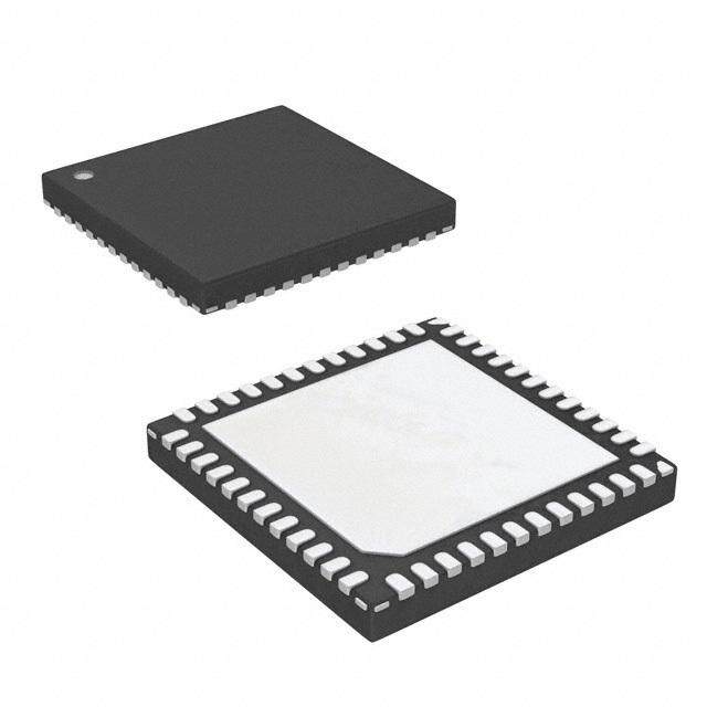
| 产品图片 |
|
| rohs | 符合RoHS无铅 / 符合限制有害物质指令(RoHS)规范要求 |
| 产品系列 | 电源管理 IC,专业电源管理,Micrel MIC5162YMM- |
| 数据手册 | |
| 产品型号 | MIC5162YMM |
| PCN组件/产地 | |
| 产品目录页面 | |
| 产品种类 | 专业电源管理 |
| 供应商器件封装 | 10-MSOP |
| 其它名称 | 576-1820-5 |
| 包装 | 管件 |
| 商标 | Micrel |
| 安装类型 | 表面贴装 |
| 安装风格 | SMD/SMT |
| 封装 | Tube |
| 封装/外壳 | 10-TFSOP,10-MSOP(0.118",3.00mm 宽) |
| 封装/箱体 | MSOP-10 |
| 工作温度 | -40°C ~ 125°C |
| 工厂包装数量 | 100 |
| 应用 | 控制器,DDR3,GDDR3/4/5 |
| 标准包装 | 100 |
| 电压-输入 | 1.35 V ~ 6 V |
| 电压-输出 | 可编程 |
| 电源电流 | 15 mA |
| 系列 | MIC5162 |
| 输出数 | 1 |


- 商务部:美国ITC正式对集成电路等产品启动337调查
- 曝三星4nm工艺存在良率问题 高通将骁龙8 Gen1或转产台积电
- 太阳诱电将投资9.5亿元在常州建新厂生产MLCC 预计2023年完工
- 英特尔发布欧洲新工厂建设计划 深化IDM 2.0 战略
- 台积电先进制程称霸业界 有大客户加持明年业绩稳了
- 达到5530亿美元!SIA预计今年全球半导体销售额将创下新高
- 英特尔拟将自动驾驶子公司Mobileye上市 估值或超500亿美元
- 三星加码芯片和SET,合并消费电子和移动部门,撤换高东真等 CEO
- 三星电子宣布重大人事变动 还合并消费电子和移动部门
- 海关总署:前11个月进口集成电路产品价值2.52万亿元 增长14.8%


PDF Datasheet 数据手册内容提取
MIC5162 Dual Regulator Controller for DDR3 GDDR3/4/5 Memory and High-Speed Bus Termination General Description Features The MIC5162 is a dual regulator controller designed for • Input voltage range: 1.35V to 6V high speed bus termination. It offers a simple, low-cost • Up to 7A V Current TT JEDEC compliant solution for terminating high-speed, low- • Tracking programmable output voltage digital buses (i.e. DDR, DDR2, DDR3, SCSI, GTL, SSTL, HSTL, LV-TTL, Rambus, LV-PECL, LV-ECL, etc). • Wide bandwidth The MIC5162 controls two external N-Channel MOSFETs • Logic controlled enable input to form two separate regulators. It operates by switching • Requires minimal external components between either the high-side MOSFET or the low-side • DDR, DDR2, DDR3, memory termination MOSFET depending upon whether the current is being • -40°C < T < +125°C sourced to the load or sunk by the regulator. J • JEDEC Compliant Bus Termination for SCSI, GTL, Designed to provide a universal solution for bus SSTL, HSTL, LV-TTL, Rambus, LV-PECL, LV-ECL, etc termination regardless of input voltage, output voltage, or • Tiny MSOP-10 package load current. The desired MIC5162 output voltage can be programmed by forcing the reference voltage externally to desired voltage. Applications The MIC5162 operates from an input of 1.35V to 6V, with • Desktop Computers a second bias supply input required for operation. It is available in a tiny MSOP-10 package with operating • Notebook computers junction temperature range of -40°C to +125°C. • Communication systems Data sheets and support documentation can be found on • Video cards Micrel’s web site at: www.micrel.com. • DDR/DDR2/DDR3 memory termination ____________________________________________________________________________________________________________ Typical Application Typical SSTL-2 Application (Two MOSFETs Support a 3.5A Application) Micrel Inc. • 2180 Fortune Drive • San Jose, CA 95131 • USA • tel +1 (408) 944-0800 • fax + 1 (408) 474-1000 • http://www.micrel.com March 2010 M9999-033110
Micrel, Inc. MIC5162 Ordering Information Part Number Temperature Range Package Lead Finish MIC5162YMM –40° to +125°C 10-Pin MSOP Pb-Free Note: MSOP is a Green RoHS compliant package. Lead finish is NiPdAu. Mold compound is Halogen Free. Pin Configuration 10-Pin MSOP (MM) Pin Description Pin Number Pin Name Pin Function 1 VCC Bias Supply Input. Apply 3V-6V to this input for internal bias to the controller. 2 EN Enable (Input): CMOS compatible input. Logic high = enable, logic low = shutdown. The enable pin can be tied directly to V or V for functionality. Do not float the DDQ CC enable pin. Floating this pin causes the enable to be in an undetermined state. 3 VDDQ Input Supply Voltage. 4 VREF Reference voltage equal to half of VDDQ. For internal use only. 5 GND Ground. 6 FB Feedback input to the internal error amplifier. 7 COMP Compensation (Output): Connect a capacitor and resistor from COMP pin to feedback pin for compensation of the internal control loop. 8 LD Low-side drive: Connects to the Gate of the external low-side MOSFET. 9 HD High-side drive: Connects to the Gate of the external high-side MOSFET. 10 NC Not internally connected. March 2010 2 M9999-033110
Micrel, Inc. MIC5162 Absolute Maximum Ratings(1) Operating Ratings(2) Supply Voltage (V ).......................................−0.3V to +7V Supply Voltage (V )..............................................3V to 6V CC CC Supply Voltage (VDDQ).....................................−0.3V to +7V Supply Voltage (VDDQ).......................................1.35V to 6V Enable Input Voltage (VEN)....................−0.3V to (VIN+0.3V) Enable Input Voltage (VEN).....................................0V to VIN Junction Temperature Range (T )......−40°C < T < +125°C Junction Thermal Resistance J J Lead Temperature (Soldering 10sec.).......................260°C MSOP-10 (θJA)..............................................130.5°C/W Storage Temperature (T ).........................−65°C to +150°C MSOP-10 (θJC)................................................42.6°C/W S ESD Rating(3)................................................................+2kV Electrical Characteristics(4) T = 25°C with V = 2.5V; V = 5V, V = V , bold values indicate –40°C ≤ T ≤ +125°C, unless otherwise specified. A DDQ CC EN CC J See test circuit 1 for test circuit configuration. Parameter Condition Min Typ Max Units V Voltage Accuracy -1% 0.5V +1% V REF DDQ V Voltage Accuracy (Note 5) Sourcing; 100mA to 3A -5 0.4 +5 mV TT -10 +10 mV Sinking; -100mA to -3A -5 0.6 +5 mV -10 +10 mV Supply Current (I ) V = 1.2V (controller ON) 120 140 µA DDQ EN No Load 200 µA Supply Current (I ) No Load 15 20 mA CC 25 mA I Shutdown Current (Note 6) V = 0.2V (controller OFF) 10 35 µA CC EN Start-up Time (Note 7) V = 5V external bias; V = V 8 15 µs CC EN IN 30 µs Enable Input Regulator Enable 1.2 V Enable Input Threshold Regulator Shutdown 0.3 V Enable Hysteresis 40 mV V < 0.2V (controller shutdown) 0.01 µA IL Enable Pin Input Current V > 1.2V (controller enable) 5.5 µA IH Driver High Side MOSFET Fully ON 4.8 4.97 V High Side Gate Drive Voltage High Side MOSFET Fully OFF 0.03 0.2 V Low Side MOSFET Fully ON 4.8 4.97 V Low Side Gate Drive Voltage Low Side MOSFET Fully OFF 0.03 0.2 V Notes: 1. Exceeding the absolute maximum rating may damage the device. 2. The device is not guaranteed to function outside its operating rating. 3. Devices are ESD sensitive. Handling precautions recommended. Human body model 1.5kΩ in series with 100pF. 4. Specification for packaged product only. 5. The V voltage accuracy is measured as a delta voltage from the reference output (V - V ). TT TT REF 6. Shutdown current is measured only on the V pin. The V pin will always draw a minimum amount of current when voltage is applied. CC DDQ 7. Start-up time is defined as the amount of time from EN = V to HSD = 90% of V . CC CC March 2010 3 M9999-033110
Micrel, Inc. MIC5162 Test Circuit March 2010 4 M9999-033110
Micrel, Inc. MIC5162 Typical Characteristics [VTT - VREF] [VTT - VREF] [VTT - VREF] vs. Output Current vs. Temperature vs. Temperaute 5 10 10 4 8 8 3 6 6 mV) 2 mV) 4 mV) 4 ] (F 1 ] (F 2 ] (F 2 RE 0 RE 0 RE 0 V V V - T-1 - T -2 - T -2 VT-2 VT -4 VT -4 [ [ [ -3 -6 -6 -4 -8 -8 SINK 3A SOURCE 3A -5 -10 -10 -3 -2 -1 0 1 2 3 -40 -20 0 20 40 60 80 100120 -40 -20 0 20 40 60 80 100120 OUTPUT CURRENT (A) TEMPERATURE (ºC) TEMPERATURE (ºC) VREF ICC Current ICC Current vs. Temperature vs. VCC vs. Temperature 1.2625 18 20 1.2600 VDDQ = 2.5V A)16 A)18 1.2575 m14 m16 1.2550 T ( T (14 N12 N V (V)REF1111....2222445557020505 CE CURRE1680 CE CURRE116802 R R 1.2425 U 4 U 4 O O 1.2400 S 2 S 2 VCC = 5V 1.2375 0 0 -40 -20 0 20 40 60 80 100120 0 1 2 3 4 5 6 -40 -20 0 20 40 60 80 100120 TEMPERATURE (ºC) INPUT VOLTAGE (V) TEMPERATURE (ºC) March 2010 5 M9999-033110
Micrel, Inc. MIC5162 Functional Diagram March 2010 6 M9999-033110
Micrel, Inc. MIC5162 Application Information V DDQ The V pin on the MIC5162 provides the source High performance memory requires high speed DDQ current through the high-side N-Channel and the signaling. This means special attention must be paid to reference voltage to the device. The MIC5162 can maintain signal integrity. Bus termination provides a operate at V voltages as low as 1.35V. Due to the means to increase signaling speed while maintaining DDQ possibility of large transient currents being sourced from good signal integrity. An example of bus termination is this line, significant bypass capacitance will aid in the Series Stub Termination Logic or SSTL. Figure 1 is performance by improving the source impedance at an example of an SSTL 2 single ended series parallel higher frequencies. Since the reference is simply V /2, terminated output. SSTL 2 is a JEDEC signaling DDQ perturbations on the V will also appear at half the standard operating off a 2.5V supply. It consists of a DDQ amplitude on the reference. For this reason, low ESR series resistor (R ) and a terminating resistor (R ). S T capacitors such as ceramics or OS-CON are Values of R range between 10Ω to 30Ω with a typical of S recommended on V . 22Ω, while R ranges from 22Ω to 28Ω with a typical DDQ T value of 25Ω. V must maintain 1/2 VDD with a ±1% REF V TT tolerance, while V will dynamically sink and source TT V is the actual termination point. V is regulated to current to maintain a termination voltage of ±40mV from TT TT V . Due to high speed signaling, the load current seen the V line under all conditions. This method of bus REF REF by V is constantly changing. To maintain adequate termination reduces common mode noise, settling time, TT large signal transient response, large OS-CON and voltage swings, EMI/RFI and improves slew rates. ceramics are recommended on V . The proper TT The MIC5162 is a high performance linear controller, combination and placement of the OS-CON and ceramic utilizing scalable N-Channel MOSFETs to provide capacitors is important to reduce both ESR and ESL JEDEC-compliant bus termination. Termination is such that high-current and high-speed transients do not achieved by dividing down the V voltage by half, DDQ exceed the dynamic voltage tolerance requirement of providing the reference (V ) voltage. An internal error REF V . The larger OS-CON capacitors provide bulk charge TT amplifier compares the termination voltage (V ) and TT storage while the smaller ceramic capacitors provide V , controlling 2 external N-Channel MOSFETs to sink REF current during the fast edges of the bus transition. Using and source current to maintain a termination voltage several smaller ceramic capacitors distributed near the (V ) equal to V . The N-Channels receive their TT REF termination resistors is typically important to reduce the enhancement voltage from a separate V pin on the CC effects of PCB trace inductance. device. Although this document focuses mostly on SSTL, the VREF MIC5162 is also capable of providing bus terminations Two resistors dividing down the V voltage provide DDQ for SCSI, GTL, HSTL, LV-TTL, Rambus, LV-PECL, V (Figure 3). The resistors are valued at around REF DDR, DDR2, DDR3 memory termination and other 17kΩ. A minimum capacitor value of 120pF from V to REF systems. ground is required to remove high frequency signals reflected from the source. Large capacitance values (>1500pF) should be avoided. Values greater than 1500pF slow down V and detract from the reference REF voltage’s ability to track V during high speed load DDQ transients. Figure 1. SSTL-2 Termination Figure 2. MIC5162 as a DDR Memory Termination for 3.5A Application March 2010 7 M9999-033110
Micrel, Inc. MIC5162 Input Capacitance Although the MIC5162 does not require an input capacitor for stability, using one greatly improves device performance. Due to the high-speed nature of the MIC5162, low ESR capacitors such as OS-CON and ceramics are recommended for bypassing the input. The recommended value of capacitance will depend greatly upon proximity to the bulk capacitance. Although a 10µF ceramic capacitor will suffice for most applications, input Figure 3. VREF Follows VDDQ capacitance may need to be increased in cases where the termination circuit is greater than 1 inch away from VREF can also be manipulated for different applications. the bulk capacitance. A separate voltage source can be used to externally set the reference point, bypassing the divider network. Also, Output Capacitance external resistors can be added from VREF-to-VDDQ or Large, low ESR capacitors are recommended for the VREF-to-ground to shift the reference point up or down. output (VTT) of the MIC5162. Although low ESR capacitors are not required for stability, they are V CC recommended to reduce the effects of high-speed VCC supplies the internal circuitry of the MIC5162 and current transients on VTT. The change in voltage during provides the drive voltage to enhance the external N- the transient condition will be the effect of the peak Channel MOSFETs. A 1µF ceramic capacitor is current multiplied by the output capacitor’s ESR. For that recommended for bypassing the VCC pin. The minimum reason, OS-CON type capacitors are excellent for this VCC voltage should be a gate-source voltage above VTT application. They have extremely low ESR and large or greater than 3V without exceeding 6V. For example, capacitance-to-size ratio. Ceramic capacitors are also on an SSTL compliant terminator, VDDQ equals 2.5V and well suited to termination due to their low ESR. These VTT equals 1.25V. If the N-Channel MOSFET selected capacitors should have a dielectric rating of X5R or X7R. requires a gate source voltage of 2.5V, VCC should be a Y5V and Z5U type capacitors are not recommended, minimum of 3.75V. due to their poor performance at high frequencies and over temperature. The minimum recommended Feedback and Compensation capacitance for a 3 Amp peak circuit is 100µF. Output The feedback provides the path for the error amplifier to capacitance can be increased to achieve greater regulate VTT. An external resistor must be placed transient performance. between the feedback and V . This allows the error TT amplifier to be correctly externally compensated. MOSFET Selection The COMP pin on the MIC5162 is the output of the The MIC5162 utilizes external N-Channel MOSFETs to internal error amplifier. By placing a capacitor between sink and source current. MOSFET selection will settle to the COMP pin and the feedback pin, this coupled with two main categories: size and gate threshold (V ). GS the feedback resistor places an external pole on the MOSFET Power Requirements error amplifier. With a 1kΩ or 510Ω feedback resistor, a minimum 220pF capacitor is recommended for a 3.5A One of the most important factors is to determine the peak termination circuit. Increases in load, multiple N- amount of power the MOSFET required to dissipate. Channel MOSFETs and/or increase in output Power dissipation in an SSTL circuit will be identical for capacitance may require feedback and/or compensation both the high-side and low-side MOSFETs. Since the capacitor values to be increased to maintain stability. supply voltage is divided by half to supply V , both TT Feedback resistor values should not exceed 10kΩ and MOSFETs have the same voltage dropped across them. compensation capacitors should not be less than 40pF. They are also required to be able to sink and source the same amount of current (for either all 0s or all 1s). This Enable equates to each side being able to dissipate the same The MIC5162 features an active-high enable (EN) input. amount of power. Power dissipation calculation for the In the off-mode state, leakage currents are reduced to high-side driver is as follows: microamperes. EN has thresholds compatible with P = (V − V ) × I_SOURCE TTL/CMOS for simple logic interfacing. EN can be tied D DDQ TT where I_SOURCE is the average source current. Power directly to V or V for functionality. Do not float the DDQ CC dissipation for the low-side MOSFET is as follows: EN pin. Floating this pin causes the enable circuitry to be in an undetermined state. P = V × I_SINK D TT March 2010 8 M9999-033110
Micrel, Inc. MIC5162 where I_SINK is the average sink current. θ =32.5°C/W JA In a typical 3A peak SSTL_2 circuit, power This shows that our total thermal resistance must be considerations for MOSFET selection would occur as better than 32.5°C/W. Since the total thermal resistance follows. is a combination of all the individual thermal resistances, P = (V −V ) × I_SOURCE the amount of heat sink required can be calculated as D DDQ TT follows: P = (2.5V −1.25V) × 1.6A D θ = θ − (θ + θ ) P = 2W SA JA JC CS D In this example: This typical SSTL_2 application would require both high- side and low-side N-Channel MOSFETs to be able to θ =32.5°C/W -(1.5°C/W +0.5°C) SA handle 2 Watts each. In applications where there is θ = 30.5°C / W excessive power dissipation, multiple N-Channel SA MOSFETs may be placed in parallel. These MOSFETs In most cases, case-to-sink thermal resistance can be will share current, distributing power dissipation across assumed to be about 0.5°C/W. each device. The SSTL termination circuit for this example, using 2 D- The maximum MOSFET die (junction) temperature limits pack N-Channel MOSFETs (one high side and one on maximum power dissipation. The ability of the device to the low side) will require at least a 30.5°C/W heat sink dissipate heat away from the junction is specified by the per MOSFET. This may be accomplished with an junction-to-ambient (θJA) thermal resistance. This is the external heat sink or even just the copper area that the sum of junction-to-case (θJC) thermal resistance, case- MOSFET is soldered to. In some cases, airflow may also to-sink (θCS) thermal resistance and sink-to-ambient be required to reduce thermal resistance. (θ ) thermal resistance; SA MOSFET Gate Threshold θ = θ + θ + θ JA JC CS SA N-Channel MOSFETs require an enhancement voltage In the example of a 3A peak SSTL_2 termination circuit, greater than its source voltage. Typical N-Channel a D-pack N-Channel MOSFET that has a maximum MOSFETs have a gate-source threshold (V ) of 1.8V junction temperature of 125°C has been selected. The GS and higher. Since the source of the high side N-Channel device has a junction-to-case thermal resistance of is connected to V , the MIC5162 V pin requires a 1.5°C/Watt. The application has a maximum ambient TT CC voltage greater than the V voltage. For example, the temperature of 60°C. The required junction-to-ambient GS SSTL_2 termination circuit has a V voltage of 1.25V. thermal resistance can be calculated as follows: TT For an N-Channel that has a V rating of 2.5V, the V GS CC θ = TJ −TA voltage can be as low as 3.75V, but not less than 3.0V. JA P With an N-Channel that has a 4.5V V , the minimum D GS V required is 5.75V. Although these N-Channels are Where T is the maximum junction temperature, T is the CC J A driven below their full enhancement threshold, it is maximum ambient temperature and P is the power D recommended that the V voltage has enough margin dissipation. CC to be able to fully enhance the MOSFETs for large signal In this example: transient response. In addition, low gate thresholds θJA = TJP−TA MreOquSirFeEmTesn tsa. re recommended to reduce the VCC D 125°C-60°C θ = JA 2W March 2010 9 M9999-033110
Micrel, Inc. MIC5162 VIN or VDDQ MIC5162YMM SUD50N02-06P VDDQ=1.35V to 6.0V VDDQ HD VTT=½VDDQ VCC=5.0V VCC SUD50N02-06P 1k LD EN COMP + EN 1k 100µF 100µF + 220pF 100µF 100µF 1µF VREF FB GND 1k 120pF Figure 4. DDR2 Termination (Four MOSFETs Support up to 7A) SSTL-2 Application (Two MOSFETs Support up to 3.5A) March 2010 10 M9999-033110
Micrel, Inc. MIC5162 Ripple Measurements To properly measure ripple on either input or output of a switching regulator, a proper ring in tip measurement is required. Standard oscilloscope probes come with a grounding clip, or a long wire with an alligator clip. Unfortunately, for high frequency measurements, this ground clip can pick up high frequency noise and erroneously inject it into the measured output ripple. The standard evaluation board accommodates a home made version by providing probe points for both the input and output supplies and their respective grounds. This requires the removing of the oscilloscope probe sheath and ground clip from a standard oscilloscope probe and wrapping a non-shielded bus wire around the oscilloscope probe. If there does not happen to be any non-shielded bus wire immediately available, the leads from axial resistors will work. By maintaining the shortest possible ground lengths on the oscilloscope probe, true ripple measurements can be obtained. Figure 5. Low Noise Measurement March 2010 11 M9999-033110
Micrel, Inc. MIC5162 PCB Layout Guideline Warning!!! To minimize EMI and output noise, follow Output Capacitor these layout recommendations. • Use a wide trace to connect the output capacitor PCB Layout is critical to achieve reliable, stable and ground terminal to the input capacitor ground efficient performance. A ground plane is required to terminal. control EMI and minimize the inductance in power, • Phase margin will change as the output capacitor signal and return paths. value and ESR changes. Contact the factory if the The following guidelines should be followed to insure output capacitor is different from what is shown in proper operation of the MIC5162 controller application. the BOM. • The feedback trace should be separate from the IC and MOSFET power trace and connected as close as possible to • Place the IC close to the point of load (POL). the output capacitor. Sensing a long high current • The trace connecting controller drive pins to load trace can degrade the DC load regulation. MOSFETs gates should be short and wide to avoid oscillations. These oscillations are the result of tank circuit formed by trace inductance and gate capacitance. • Use fat traces to route the input and output power lines. • Signal and power grounds should be kept separate and connected at only one location. Input Capacitor • Place the input capacitor next. • Place the input capacitors on the same side of the board and as close to the MOSFET and IC as possible. • Place a ceramic bypass capacitor next to MOSFET. • Keep both the VDDQ and GND connections short. • Place several vias to the ground plane close to the input capacitor ground terminal, but not between the input capacitors and MOSFET. • Use either X7R or X5R dielectric input capacitors. Do not use Y5V or Z5U type capacitors. • Do not replace the ceramic input capacitor with any other type of capacitor. Any type of capacitor can be placed in parallel with the input capacitor. • If a Tantalum input capacitor is placed in parallel with the input capacitor, it must be recommended for switching regulator applications and the operating voltage must be derated by 50%. • In “Hot-Plug” applications, a Tantalum or Electrolytic bypass capacitor must be used to limit the over- voltage spike seen on the input supply with power is suddenly applied. March 2010 12 M9999-033110
Micrel, Inc. MIC5162 Design Example Micrel’s MIC5162 as a DDR3 Memory Termination Device for 3.5A Application (VDDQ and MOSFET Input Tied Together) Bill of Materials Item Part Number Manufacturer Description Qty. GRM21BR60J226ME39L Murata(1) C1, C2, C2012X5R0J226M TDK(2) 22µF, 6.3V, Ceramic capacitor, X5R, 0805 4 C3, C4 08056D226MAT2A AVX(3) GRM188R60J106ME47D Murata(1) C5 C1608X5R0J106M TDK(2) 10µF, 6.3V, Ceramic capacitor, X5R, 0603 1 06036D106MAT2A AVX(3) GRM1885C1H390JA01D Murata(1) 39pF, 50V, Ceramic capacitor, NPO, 0603 C6 1 C1608C0G1H390J TDK(2) 39pF, 25V, Ceramic capacitor, NPO, 0603 C7 06035C101MAT2A AVX(3) 100pF, 50V, Ceramic capacitor, X7R, 0603 1 C8 GRM188R71H391KA01D Murata(1) 390pF, 50V, Ceramic capacitor, X7R, 0603 1 GRM31CR60J476ME19L Murata(1) C9, C10 C3216X5R0J476M TDK(2) 47µF, 6.3V, Ceramic capacitor, X5R, 1206 2 12066D476MAT2A AVX(3) C13 GRM188R71H102KA01D Murata(1) 1nF, 50V, Ceramic capacitor, X7R, 0603 1 C14 GRM188R71H103KA01D Murata(1) 10nF, 50V, Ceramic capacitor, X7R, 0603 1 0603ZD105KAT2A AVX(3) 1 C22 1µF, 10V, Ceramic capacitor, X5R, 0603 GRM188R61A105K Murata(1) VJ0603A121JXACW1BC Vishay(4) 2 C23, C12 120pF, 25V, Ceramic capacitor, NPO, 0603 06033A121JAT2A AVX(3) VJ0603Y221KXACW1BC Vishay(4) 220pF, 50V, Ceramic capacitor, X7R, 0603 1 C27 06033C221JAT2A AVX(3) 220pF, 25V, Ceramic capacitor, X7R, 0603 C26 TCJB107M006R0070 AVX(3) 100µF, 6.3V, Tantalum capacitor, 1210 1 C24, C11 N.U. 0603 ceramic cap March 2010 13 M9999-033110
Micrel, Inc. MIC5162 Item Part Number Manufacturer Description Qty. C30, C32, C4532X5R0J107M TDK(2) 100µF, 6.3V, Ceramic capacitor, X5R, 1812 3 C21 C31 Open (2SEPC2700M) Sanyo(5) 2700µF, 2.5V OS-CON Cap 1 CIN EEE-FPA122UAP Panasonic(8) 1200µF, 10V, Electrolytic capacitor, SMD, 10x10.2-case 1 L1 CDEP105ME-1R2MC Sumida(6) 1.2µH, 21A, Inductor, 10.4mmX10.4mm 1 Q1 2N7002E(SOT-23) Vishay(4) Signal MOSFET, SOT-23-6 1 Q21, Q22 SUD50N02-06P Vishay(4) Low VGS(th) N-Channel 20-V (D-S) 2 R1 CRCW0603820RFRT1 Vishay Dale(4) 820Ω, Resistor, 1%, 0603 1 R2 CRCW0603698RFRT1 Vishay Dale(4) 698Ω, Resistor, 1%, 0603 1 R3 CRCW06032002FRT1 Vishay Dale(4) 20K, Resistor, 1%, 0603 1 R4 CRCW06034752FRT1 Vishay Dale(4) 47.5K, Resistor, 1%, 0603 1 R5 CRCW06031003FRT1 Vishay Dale(4) 100K, Resistor, 1%, 0603 1 R21 CRCW0805510RFKTA Vishay Dale(4) 510Ω, Resistor, 1%, 0805 1 R23, R24 CRCW06031K00FKTA Vishay Dale(4) 1K, Resistor, 1%, 0603 2 R22 CRCW06030000FKTA Vishay Dale(4) 0Ω, Resistor, 1%, 0603 1 U1 MIC22950YML Micrel(7) Buck Regulator 10A, 0.4MHz-2MHz Synchronous 1 Buck Regulator U21 MIC5162YMM Micrel(7) Dual Regulator Controller for DDR3 1 Notes: 1. Murata: www.murata.com. 2. TDK: www.tdk.com. 3. AVX: www.avx.com. 4. Vishay: www.vishay.com. 5. Sanyo: www.sanyo.com 6. Sumida: www.sumida.com 7. Micrel, Inc.: www.micrel.com. 8. Panasonic.: www.panasonic.com March 2010 14 M9999-033110
Micrel, Inc. MIC5162 PCB Layout Recommendations (VDDQ and MOSFET Input Tied Together) Top Layer Top Component Layer March 2010 15 M9999-033110
Micrel, Inc. MIC5162 Middle Layer 1 Middle Layer 2 March 2010 16 M9999-033110
Micrel, Inc. MIC5162 Bottom Layer March 2010 17 M9999-033110
Micrel, Inc. MIC5162 Design Example Micrel’s MIC5162 as a DDR3 Memory Termination Device for 3.5A Application (VDDQ and MOSFET Input Separated) Bill of Materials Item Part Number Manufacturer Description Qty. GRM21BR60J226ME39L Murata(1) C1, C2, C2012X5R0J226M TDK(2) 22µF, 6.3V, Ceramic capacitor, X5R, 0805 4 C3, C4 08056D226MAT2A AVX(3) GRM188R60J106ME47D Murata(1) C5 C1608X5R0J106M TDK(2) 10µF, 6.3V, Ceramic capacitor, X5R, 0603 1 06036D106MAT2A AVX(3) GRM1885C1H390JA01D Murata(1) 39pF, 50V, Ceramic capacitor, NPO, 0603 1 C6 C1608C0G1H390J TDK(2) 39pF, 25V, Ceramic capacitor, NPO, 0603 C7 06035C101MAT2A AVX(3) 100pF, 50V, Ceramic capacitor, X7R, 0603 1 C8 GRM188R71H391KA01D Murata(1) 390pF, 50V, Ceramic capacitor, X7R, 0603 1 GRM31CR60J476ME19L Murata(1) C9, C10 C3216X5R0J476M TDK(2) 47µF, 6.3V, Ceramic capacitor, X5R, 1206 2 12066D476MAT2A AVX(3) C13 GRM188R71H102KA01D Murata(1) 1nF, 50V, Ceramic capacitor, X7R, 0603 1 C14 GRM188R71H103KA01D Murata(1) 10nF, 50V, Ceramic capacitor, X7R, 0603 1 0603ZD105KAT2A AVX(3) 2 C22, C28 1µF, 10V, Ceramic capacitor, X5R, 0603 GRM188R61A105K Murata(1) VJ0603A121JXACW1BC Vishay(4) 2 C23, C12 120pF, 25V, Ceramic capacitor, NPO, 0603 06033A121JAT2A AVX(3) VJ0603Y221KXACW1BC Vishay(4) 220pF, 50V, Ceramic capacitor, X7R, 0603 1 C27 06033C221JAT2A AVX(3) 220pF, 25V, Ceramic capacitor, X7R, 0603 C26 TCJB107M006R0070 AVX(3) 100µF, 6.3V, Tantalum capacitor, 1210 1 C24, C11 N.U. 0603 ceramic cap March 2010 18 M9999-033110
Micrel, Inc. MIC5162 Item Part Number Manufacturer Description Qty. C30, C32, C4532X5R0J107M TDK(2) 100µF, 6.3V, Ceramic capacitor, X5R, 1812 3 C21 C31 Open (2SEPC2700M) Sanyo(5) 2700µF, 2.5V OS-CON Cap 1 CIN EEE-FPA122UAP Panasonic(8) 1200µF, 10V, Electrolytic capacitor, SMD, 10x10.2-case 1 L1 CDEP105ME-1R2MC Sumida(6) 1.2µH, 21A, Inductor, 10.4mmX10.4mm 1 Q1 2N7002E(SOT-23) Vishay(4) Signal MOSFET, SOT-23-6 1 Q21, Q22 SUD50N02-06P Vishay(4) Low VGS(th) N-Channel 20-V (D-S) 2 R1 CRCW0603820RFRT1 Vishay Dale(4) 820Ω, Resistor, 1%, 0603 1 R2 CRCW0603698RFRT1 Vishay Dale(4) 698Ω, Resistor, 1%, 0603 1 R3 CRCW06032002FRT1 Vishay Dale(4) 20K, Resistor, 1%, 0603 1 R4 CRCW06034752FRT1 Vishay Dale(4) 47.5K, Resistor, 1%, 0603 1 R5 CRCW06031003FRT1 Vishay Dale(4) 100K, Resistor, 1%, 0603 1 R21 CRCW0805510RFKTA Vishay Dale(4) 510Ω, Resistor, 1%, 0805 1 R23, R24 CRCW06031K00FKTA Vishay Dale(4) 1K, Resistor, 1%, 0603 2 R22 CRCW06030000FKTA Vishay Dale(4) 0Ω, Resistor, 1%, 0603 1 U1 MIC22950YML Micrel(7) Buck Regulator 10A, 0.4MHz-2MHz Synchronous 1 Buck Regulator U21 MIC5162YMM Micrel(7) Dual Regulator Controller for DDR3 1 Notes: 1. Murata: www.murata.com. 2. TDK: www.tdk.com. 3. AVX: www.avx.com. 4. Vishay: www.vishay.com. 5. Sanyo: www.sanyo.com 6. Sumida: www.sumida.com 7. Micrel, Inc.: www.micrel.com. 8. Panasonic.: www.panasonic.com March 2010 19 M9999-033110
Micrel, Inc. MIC5162 PCB Layout Recommendations (VDDQ and MOSFET Input Separated) Top Layer Top Component Layer March 2010 20 M9999-033110
Micrel, Inc. MIC5162 Middle Layer 1 Middle Layer 2 March 2010 21 M9999-033110
Micrel, Inc. MIC5162 Bottom Layer March 2010 22 M9999-033110
Micrel, Inc. MIC5162 Package Information 10-Pin MSOP (MM) March 2010 23 M9999-033110
Micrel, Inc. MIC5162 Recommended Landing Pattern 10-Pin MSOP (MM) MICREL, INC. 2180 FORTUNE DRIVE SAN JOSE, CA 95131 USA TEL +1 (408) 944-0800 FAX +1 (408) 474-1000 WEB http://www.micrel.com The information furnished by Micrel in this data sheet is believed to be accurate and reliable. However, no responsibility is assumed by Micrel for its use. Micrel reserves the right to change circuitry and specifications at any time without notification to the customer. Micrel Products are not designed or authorized for use as components in life support appliances, devices or systems where malfunction of a product can reasonably be expected to result in personal injury. Life support devices or systems are devices or systems that (a) are intended for surgical implant into the body or (b) support or sustain life, and whose failure to perform can be reasonably expected to result in a significant injury to the user. A Purchaser’s use or sale of Micrel Products for use in life support appliances, devices or systems is a Purchaser’s own risk and Purchaser agrees to fully indemnify Micrel for any damages resulting from such use or sale. © 2003 Micrel, Incorporated. March 2010 24 M9999-033110
Mouser Electronics Authorized Distributor Click to View Pricing, Inventory, Delivery & Lifecycle Information: M icrochip: MIC5162YMM MIC5162YMM-TR