ICGOO在线商城 > 集成电路(IC) > PMIC - 栅极驱动器 > MIC5011YM

 Datasheet下载
- 型号: MIC5011YM
- 制造商: Micrel
- 库位|库存: xxxx|xxxx
- 要求:
| 数量阶梯 | 香港交货 | 国内含税 |
| +xxxx | $xxxx | ¥xxxx |
查看当月历史价格
查看今年历史价格
MIC5011YM产品简介:
ICGOO电子元器件商城为您提供MIC5011YM由Micrel设计生产,在icgoo商城现货销售,并且可以通过原厂、代理商等渠道进行代购。 MIC5011YM价格参考¥询价-¥询价。MicrelMIC5011YM封装/规格:PMIC - 栅极驱动器, High-Side or Low-Side Gate Driver IC Non-Inverting 8-SOIC。您可以下载MIC5011YM参考资料、Datasheet数据手册功能说明书,资料中有MIC5011YM 详细功能的应用电路图电压和使用方法及教程。
| 参数 | 数值 |
| 产品目录 | 集成电路 (IC)半导体 |
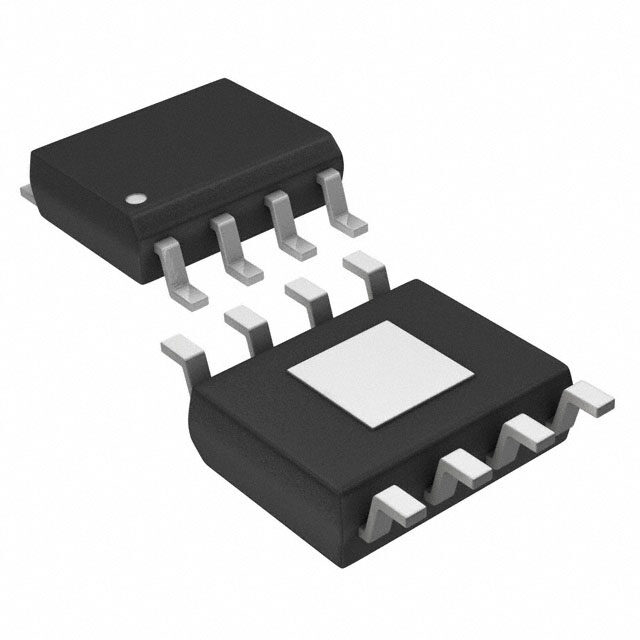
| 描述 | IC DRIVER MIN PARTS HI/LO 8SOIC门驱动器 High Side MOSFET Predriver - Lead Free |
| 产品分类 | PMIC - MOSFET,电桥驱动器 - 外部开关集成电路 - IC |
| 品牌 | Micrel |
| 产品手册 | |
| 产品图片 |
|
| rohs | 符合RoHS无铅 / 符合限制有害物质指令(RoHS)规范要求 |
| 产品系列 | 电源管理 IC,门驱动器,Micrel MIC5011YM- |
| 数据手册 | |
| 产品型号 | MIC5011YM |
| 产品 | MOSFET Gate Drivers |
| 产品目录页面 | |
| 产品种类 | 门驱动器 |
| 供应商器件封装 | 8-SOIC |
| 其它名称 | 576-1230 |
| 包装 | 管件 |
| 商标 | Micrel |
| 安装类型 | 表面贴装 |
| 安装风格 | SMD/SMT |
| 封装 | Tube |
| 封装/外壳 | 8-SOIC(0.154",3.90mm 宽) |
| 封装/箱体 | SOIC-8 |
| 工作温度 | -40°C ~ 85°C |
| 工厂包装数量 | 95 |
| 延迟时间 | 25µs |
| 最大功率耗散 | 1.25 W |
| 最大工作温度 | + 85 C |
| 最小工作温度 | - 40 C |
| 标准包装 | 95 |
| 激励器数量 | 1 Driver |
| 电压-电源 | 4.75 V ~ 32 V |
| 电流-峰值 | - |
| 电源电压-最大 | 32 V |
| 电源电压-最小 | 4.75 V |
| 电源电流 | 8 mA |
| 空闲时间—最大值 | 10 us |
| 类型 | High and Low Side Driver |
| 系列 | MIC5011 |
| 输入类型 | 非反相 |
| 输出数 | 1 |
| 输出端数量 | 1 |
| 配置 | 高端或低端 |
| 配置数 | 1 |
| 高压侧电压-最大值(自举) | - |


- 商务部:美国ITC正式对集成电路等产品启动337调查
- 曝三星4nm工艺存在良率问题 高通将骁龙8 Gen1或转产台积电
- 太阳诱电将投资9.5亿元在常州建新厂生产MLCC 预计2023年完工
- 英特尔发布欧洲新工厂建设计划 深化IDM 2.0 战略
- 台积电先进制程称霸业界 有大客户加持明年业绩稳了
- 达到5530亿美元!SIA预计今年全球半导体销售额将创下新高
- 英特尔拟将自动驾驶子公司Mobileye上市 估值或超500亿美元
- 三星加码芯片和SET,合并消费电子和移动部门,撤换高东真等 CEO
- 三星电子宣布重大人事变动 还合并消费电子和移动部门
- 海关总署:前11个月进口集成电路产品价值2.52万亿元 增长14.8%


PDF Datasheet 数据手册内容提取
MIC5011 Micrel, Inc. MIC5011 Minimum Parts High- or Low-Side MOSFET Driver General Description Features The MIC5011 is the “minimum parts count” member of the • 4.75V to 32V operation Micrel MIC501X driver family. These ICs are designed to • Less than 1µA standby current in the “off” state drive the gate of an N-channel power MOSFET above the • Internal charge pump to drive the gate of an N-channel supply rail in high-side power switch applications. The 8-pin power FET above supply MIC5011 is extremely easy to use, requiring only a power • Available in small outline SOIC packages FET and nominal supply decoupling to implement either a • Internal zener clamp for gate protection high- or low-side switch. • Minimum external parts count The MIC5011 charges a 1nF load in 60µs typical with no • Can be used to boost drive to low-side power FETs external components. Faster switching is achieved by add- operating on logic supplies ing two 1nF charge pump capacitors. Operation down to • 25µs typical turn-on time with optional external 4.75V allows the MIC5011 to drive standard MOSFETs in capacitors 5V low-side applications by boosting the gate voltage above • Implements high- or low-side drivers the logic supply. In addition, multiple paralleled MOSFETs can be driven by a single MIC5011 for ultra-high current Applications applications. • Lamp drivers Other members of the Micrel driver family include the • Relay and solenoid drivers MIC5013 protected 8-pin driver. • Heater switching For new designs, Micrel recommends the pin-compatible • Power bus switching MIC5014 MOSFET driver. Typical Applications Ordering Information Part Number Temperature 14.4V Standard Pb-Free Range Package ON MIC5011BN MIC5011YN –40ºC to +85ºC 8-pin Plastic + MIC5011 10µF DIP 1 V+ C1 8 MIC5011BM MIC5011YM –40ºC to +85ºC 8-pin SOIC 2 7 Control Input Input Com 3 6 Source C2 4 Gnd Gate 5 IRF531 OFF #6014 Figure 1. High Side Driver Note: The MIC5011 is ESD sensitive. 5V 48V ON 10µF + MIC5011 1 V+ C1 8 Control Input 2 Input Com 7 100W Heater 3 6 Source C2 4 Gnd Gate 5 IRF530 OFF Protected under one or more of the following Micrel patents: patent #4,951,101; patent #4,914,546 Figure 2. Low Side Driver Micrel, Inc. • 2180 Fortune Drive • San Jose, CA 95131 • USA • tel + 1 (408) 944-0800 • fax + 1 (408) 474-1000 • http://www.micrel.com July 2005 1 MIC5011
MIC5011 Micrel, Inc. Absolute Maximum Ratings (Note 1, 2) Operating Ratings (Notes 1, 2) Supply Voltage (V+), Pin 1 –0.5V to 36V Power Dissipation 1.25W Input Voltage, Pin 2 –10V to V+ θ (Plastic DIP) 100°C/W JA Source Voltage, Pin 3 –10V to V+ θ (SOIC) 170°C/W JA Current into Pin 3 50mA Ambient Temperature: B version –40°C to +85°C Gate Voltage, Pin 5 –1V to 50V Storage Temperature –65°C to +150°C Junction Temperature 150°C Lead Temperature 260°C (Soldering, 10 seconds) Supply Voltage (V+), Pin 1 4.75V to 32V high side 4.75V to 15V low side Pin Description (Refer to Typical Applications) Pin Number Pin Name Pin Function 1 V+ Supply; must be decoupled to isolate from large transients caused by the power FET drain. 10µF is recommended close to pins 1 and 4. 2 Input Turns on power MOSFET when taken above threshold (3.5V typical). Re- quires <1 µA to switch. 3 Source Connects to source lead of power FET and is the return for the gate clamp zener. Can safely swing to –10V when turning off inductive loads. 4 Ground 5 Gate Drives and clamps the gate of the power FET. Will be clamped to approxi- mately –0.7V by an internal diode when turning off inductive loads. 6, 7, 8 C2, Com, C1 Optional 1nF capacitors reduce gate turn-on time; C2 has dominant effect. Pin Configuration MIC5011 1 8 V+ C1 2 7 Input Com 3 6 Source C2 4 5 Gnd Gate MIC5011 2 July 2005
MIC5011 Micrel, Inc. Electrical Characteristics (Note 3) Test circuit. T = –55°C to +125°C, V+ = 15V, all switches open, unless otherwise specified. A Parameter Conditions Min Typical Max Units Supply Current, I V+ = 32V V = 0V, S2 closed 0.1 10 µA 1 IN V = V+ = 32V 8 20 mA IN V+ = 5V V = 5V, S2 closed 1.6 4 mA IN Logic Input Voltage V+ = 4.75V Adjust V for V low 2 V IN GATE Adjust V for V high 4.5 V IN GATE V+ = 15V Adjust V for V high 5.0 V IN GATE Logic Input Current, I V+ = 32V V = 0V –1 µA 2 IN V = 32V 1 µA IN Input Capacitance Pin 2 5 pF Gate Drive, V S1, S2 closed, V+ = 4.75V, I = 0, V = 4.5V 7 10 V GATE GATE IN V = V+, V = 5V V+ = 15V, I = 100µA, V = 5V 24 27 V S IN GATE IN Zener Clamp, S2 closed, V = 5V V+ = 15V, V = 15V 11 12.5 15 V IN S V – V V+ = 32V, V = 32V 11 13 16 V GATE SOURCE S Gate Turn-on Time, t V switched from 0 to 5V; measure time 25 50 µs ON IN (Note 4) for V to reach 20V GATE Gate Turn-off Time, t V switched from 5 to 0V; measure time 4 10 µs OFF IN for V to reach 1V GATE Note 1 Absolute Maximum Ratings indicate limits beyond which damage to the device may occur. Electrical specifications do not apply when operating the device beyond its specified Operating Ratings. Note 2 The MIC5011 is ESD sensitive. Note 3 Minimum and maximum Electrical Characteristics are 100% tested at T = 25°C and T = 85°C, and 100% guaranteed over the entire A A range. Typicals are characterized at 25°C and represent the most likely parametric norm. Note 4 Test conditions reflect worst case high-side driver performance. Low-side and bootstrapped topologies are significantly faster—see Appli- cations Information. Maximum value of switching speed seen at 125°C, units operated at room temperature will reflect the typical values shown. Test Circuit V+ + 1µF MIC5011 1 V+ C1 8 1nF 2 Input Com 7 VIN 3 Source C2 6 1nF VGATE 500Ω 1W 4 Gnd Gate 5 S2 1nF S1 I5 VS July 2005 3 MIC5011
MIC5011 Micrel, Inc. Typical Characteristics (Continued) DC Gate Voltage Supply Current above Supply 12 14 10 12 10 8 8 6 6 4 4 2 2 0 0 0 5 10 15 20 25 30 35 0 3 6 9 12 15 SUPPLY VOLTAGE (V) SUPPLY VOLTAGE (V) High-side Turn-on Time* High-side Turn-on Time* 350 140 300 120 ) S 250 CG A T E =1 nF (µ100 CG A T E =1 nF E C2=1 nF M 200 TI 80 N 150 O 60 - N 100 R 40 U T 50 20 0 0 0 3 6 9 12 15 0 3 6 9 12 15 SUPPLY VOLTAGE (V) SUPPLY VOLTAGE (V) High-side Turn-on Time* High-side Turn-on Time* 3.5 1.4 ) 3.0 S1.2 ) m S m2.5 CG A T E =10 nF E (1.0 CG A T E =10 nF E ( M C2=1 nF TIM2.0 N TI0.8 N O 1.5 -0.6 O N - R N R1.0 U0.4 T U T 0.5 0.2 0 0 0 3 6 9 12 15 0 3 6 9 12 15 SUPPLY VOLTAGE (V) SUPPLY VOLTAGE (V) * Time for gate to reach V+ + 5V in test circuit with VS = V+ – 5V. MIC5011 4 July 2005
MIC5011 Micrel, Inc. Typical Characteristics (Continued) Low-side Turn-on Time Low-side Turn-on Time for Gate = 5V for Gate = 5V 1000 1000 C2=1 nF 300 )300 ) S µS CG A T E =10 nF (µ CG A T E =10 nF E (100 E 100 M M TI TI N 30 N 30 O O - N- 10 CG A T E =1 nF N 10 R R U CG A T E =1 nF U T 3 T 3 1 1 0 3 6 9 12 15 0 3 6 9 12 15 SUPPLY VOLTAGE (V) SUPPLY VOLTAGE (V) Low-side Turn-on Time Low-side Turn-on Time for Gate = 10V for Gate = 10V 3000 3000 C2=1 nF 1000 CG A T E =10 nF 1000 S) S) µ µ CG A T E =10 nF E (300 E (300 M M TI100 TI100 N N O CG A T E =1 nF O N- 30 N- 30 CG A T E =1 nF R R U U T 10 T 10 3 3 0 3 6 9 12 15 0 3 6 9 12 15 SUPPLY VOLTAGE (V) SUPPLY VOLTAGE (V) Turn-off Time Turn-on Time 50 E 2.0 M TI S)40 CG A T E =10 nF N 1.75 µ O E ( N- 1.5 M R TI30 U N D T1.25 O 20 E N- Z 1.0 R LI U A T10 CG A T E =1 nF M0.75 R O N 0.5 0 0 3 6 9 12 15 –25 0 25 50 75 100 125 SUPPLY VOLTAGE (V) DIE TEMPERATURE (°C) July 2005 5 MIC5011
MIC5011 Micrel, Inc. Charge Pump Charge Pump Output Current Output Current A)250 A) 1.0 NT (µ200 VG A T E =V+ NT (m 0.8 VG A T E =V+ E E R R R R U150 U 0.6 C C P VG A T E =V+ +5V P M M PU100 PU 0.4 VG A T E =V + +5V E- E- G 50 G 0.2 HAR VS=V + –5V HAR VCS2==V1 +n –F5V C 0 C 0 0 5 10 15 20 25 30 0 5 10 15 20 25 30 SUPPLY VOLTAGE (V) SUPPLY VOLTAGE (V) Block Diagram Ground V+ C1ComC2 4 1 8 7 6 MIC5011 CHARGE PUMP 5 Gate 500Ω 12.5V Input 2 LOGIC 3 Source Applications Information Functional Description (Refer to Block Diagram) The charge pump incorporates a 100kHz oscillator and on- The MIC5011 functions are controlled via a logic block chip pump capacitors capable of charging 1nF to 5V above connected to the input pin 2. When the input is low, all supply in 60µs typical. With the addition of 1nF capacitors functions are turned off for low standby current and the at C1 and C2, the turn-on time is reduced to 25µs typical gate of the power MOSFET is also held low through 500Ω (see Figure 3). The charge pump is capable of pumping the to an N-channel switch. When the input is taken above the gate up to over twice the supply voltage. For this reason, a turn-on threshold (3.5V typical), the N-channel switch turns zener clamp (12.5V typical) is provided between the gate off and the charge pump is turned on to charge the gate pin 5 and source pin 3 to prevent exceeding the V rating GS of the power FET. of the MOSFET at high supplies. MIC5011 6 July 2005
MIC5011 Micrel, Inc. Applications Information (Continued) Construction Hints and it dissipates the energy stored in the load inductance. The MIC5011 source pin (3) is designed to withstand this High current pulse circuits demand equipment and assembly negative excursion without damage. External clamp diodes techniques that are more stringent than normal, low current are unnecessary. lab practices. The following are the sources of pitfalls most often encountered during prototyping. Supplies: many bench Low-Side Driver (Figure 2). A key advantage of the low- power supplies have poor transient response. Circuits that side topology is that the load supply is limited only by the are being pulse tested, or those that operate by pulse-width MOSFET BVDSS rating. Clamping may be required to modulation will produce strange results when used with a protect the MOSFET drain terminal from inductive switching supply that has poor ripple rejection, or a peaked transient transients. The MIC5011 supply should be limited to 15V in response. Always monitor the power supply voltage that low-side topologies, otherwise a large current will be forced appears at the drain of a high-side driver (or the supply through the gate clamp zener. side of the load in a low-side driver) with an oscilloscope. Low-side drivers constructed with the MIC501X family are It is not uncommon to find bench power supplies in the also fast; the MOSFET gate is driven to near supply imme- 1 kW class that overshoot or undershoot by as much as diately when commanded ON. Typical circuits achieve 10V 50% when pulse loaded. Not only will the load current and enhancement in 10µs or less on a 12 to 15V supply. voltage measurements be affected, but it is possible to Modifying Switching Times (Figure 3). High-side switch- over-stress various components—especially electrolytic ing times can be improved by a factor of 2 or more by capacitors—with possibly catastrophic results. A 10µF sup- adding external charge pump capacitors of 1nF each. In ply bypass capacitor at the chip is recommended. cost-sensitive applications, omit C1 (C2 has a dominant Residual Resistances: Resistances in circuit connections effect on speed). may also cause confusing results. For example, a circuit Do not add external capacitors to the MOSFET gate. Add a may employ a 50mΩ power MOSFET for low drop, but resistor (1kΩ to 51kΩ) in series with the gate to slow down careless construction techniques could easily add 50 to the switching time. 100mΩ resistance. Do not use a socket for the MOSFET. If the MOSFET is a TO-220 type package, make high-current drain connections to the tab. Wiring losses have a profound 14.4V effect on high-current circuits. A floating millivoltmeter can ON identify connections that are contributing excess drop + MIC5011 10µF under load. 1 V+ C1 8 1nF 2 7 Circuit Topologies Control Input Input Com The MIC5011 is suited for use with standard MOSFETs in 3 Source C2 6 1nF high- or low-side driver applications. In addition, the MIC5011 4 Gnd Gate 5 IRF531 works well in applications where, for faster switching times, OFF the supply is bootstrapped from the MOSFET source output. Low voltage, high-side drivers (such as shown in LOAD Figure 1) are the slowest; their speed is reflected in the gate turn-on time specifications. The fastest drivers are the low-side and bootstrapped high-side types (Figures 2 and 4). Load current switching times are often much faster Figure 3. High Side Driver with than the time to full gate enhancement, depending on the External Charge Pump Capacitors circuit type, the MOSFET, and the load. Turn-off times are essentially the same for all circuits (less than 10µs to V GS Bootstrapped High-Side Driver (Figure 4). The speed = 1V). The choice of one topology over another is based on of a high-side driver can be increased to better than 10µs a combination of considerations including speed, voltage, by bootstrapping the supply off of the MOSFET source. and desired system characteristics. This topology can be used where the load is pulse-width High-Side Driver (Figure 1). The high-side topology works modulated (100Hz to 20kHz), or where it is energized con- well down to V+ = 7V with standard MOSFETs. From 4.75 to tinuously. The Schottky barrier diode prevents the MIC5011 7V supply, a logic-level MOSFET can be substituted since supply pin from dropping more than 200mV below the drain the MIC5011 will not reach 10V gate enhancement (10V is supply, and it also improves turn-on time on supplies of less the maximum rating for logic-compatible MOSFETs). than 10V. Since the supply current in the “off” state is only a High-side drivers implemented with MIC501X drivers are small leakage, the 100nF bypass capacitor tends to remain self-protected against inductive switching transients. During charged for several seconds after the MIC5011 is turned turn-off an inductive load will force the MOSFET source 5V off. In a PWM application the chip supply is sustained at or more below ground, while the MIC5011 holds the gate at a higher potential than the system supply, which improves ground potential. The MOSFET is forced into conduction, switching time. July 2005 7 MIC5011
MIC5011 Micrel, Inc. Applications Information (Continued) 7 to 15V 1N5817 1N4001 (2) 100nF + 15V 10µF MIC5011 33kΩ 1 V+ C1 8 33pF To MIC5011 Control Input 2 Input Com 7 100kΩ Input 3 6 MPSA05 Source C2 4 5 4N35 Gnd Gate IRF540 10mA Control Input 100kΩ 1kΩ LOAD Figure 4. Bootstrapped Figure 5. Improved High-Side Driver Opto-Isolator Performance Opto-Isolated Interface (Figure 5). Although the MIC5011 compatible with control boxes such as the CR2943 series has no special input slew rate requirement, the lethargic (GE). The circuit is configured so that if both switches close transitions provided by an opto-isolator may cause oscil- simultaneously, the “off” button has precedence. lations on the rise and fall of the output. The circuit shown This application also illustrates how two (or more) MOS- accelerates the input transitions from a 4N35 opto-isolator FETs can be paralleled. This reduces the switch drop, and by adding hysteresis. Opto-isolators are used where the distributes the switch dissipation into multiple packages. control circuitry cannot share a common ground with the High-Voltage Bootstrap (Figure 7). Although the MIC5011 MIC5011 and high-current power supply, or where the is limited to operation on 4.75 to 32V supplies, a floating control circuitry is located remotely. This implementation is bootstrap arrangement can be used to build a high-side intrinsically safe; if the control line is severed the MIC5011 switch that operates on much higher voltages. The MIC5011 will turn OFF. and MOSFET are configured as a low-side driver, but the Industrial Switch (Figure 6). The most common manual load is connected in series with ground. control for industrial loads is a push button on/off switch. Power for the MIC5011 is supplied by a charge pump. A The “on” button is physically arranged in a recess so that 20kHz square wave (15Vp-p) drives the pump capacitor in a panic situation the “off” button, which extends out and delivers current to a 100µF storage capacitor. A zener from the control box, is more easily pressed. This circuit is 24V + 100kΩ MIC5011 10µF ON 1 V+ C1 8 CR2943-NA102A 2 7 (GE) Input Com 3 6 OFF Source C2 4 5 Gnd Gate IRFP044 (2) 330kΩ LOAD Figure 6. 50-Ampere Industrial Switch MIC5011 8 July 2005
MIC5011 Micrel, Inc. Applications Information (Continued) 15V + 100µF MIC5011 1N4746 1N4003 (2) 33kΩ 1 V+ C1 8 33pF 90V 2 7 Input Com 100kΩ MPSA05 3 6 Source C2 1nF 4 5 Gnd Gate IRFP250 4N35 10mA Control Input 100kΩ 1/4 HP, 90V 5BPB56HAA100 M (GE) 1kΩ 100nF 200V 1N4003 15Vp-p, 20kHz Squarewave Figure 7. High-Voltage Bootstrapped Driver diode limits the supply to 18V. When the MIC5011 is off, Cross conduction increases output device power dissipa- power is supplied by a diode connected to a 15V supply. The tion. Speed is also important, since PWM control requires circuit of Figure 5 is put to good use as a barrier between the outputs to switch in the 2 to 20kHz range. low voltage control circuitry and the 90V motor supply. The circuit of Figure 8 utilizes fast configurations for both Half-Bridge Motor Driver (Figure 8). Closed loop control the top- and bottom-side drivers. Delay networks at each of motor speed requires a half-bridge driver. This topology input provide a 2 to 3µs dead time effectively eliminating presents an extra challenge since the two output devices cross conduction. Two of these circuits can be connected should not cross conduct (shoot-through) when switching. together to form an H-bridge for locked antiphase or sign/ magnitude control. 15V 1N5817 1N4001 (2) 100nF 1N4148 + MIC5011 1 8 1µF V+ C1 2 7 Input Com 22kΩ 220pF 3 6 Source C2 4 5 Gnd Gate IRF541 PWM INPUT 15V + 12V, 10µF M 10A Stalled MIC5011 1 V+ C1 8 10kΩ 2 7 Input Com 22kΩ 1nF 3 Source C2 6 4 Gnd Gate 5 IRF541 2N3904 Figure 8. Half-Bridge Motor Driver July 2005 9 MIC5011
MIC5011 Micrel, Inc. Applications Information (Continued) 12V 12V + 10µF MIC5011 + 1 V+ C1 8 10µF MIC5011 2 Input Com 7 1 8 100kΩ 1N4148 V+ C1 R 3 Source C2 6 2 Input Com 7 330kΩ 330kΩ 4 Gnd Gate 5 IRFZ44 3 6 + Source C2 47µF 4 5 Gnd Gate IRFZ44 1N4148 10kΩ 100nF 100Ω OUTPUT T M (Delay=2.5s) 12V Figure 9. 30-Ampere START Time-Delay Relay RUN Time-Delay Relay (Figure 9). The MIC5011 forms the basis STOP of a simple time-delay relay. As shown, the delay commences Figure 10. Motor Stall when power is applied, but the 100kΩ/1N4148 could be Shutdown independently driven from an external source such as a switch or another high-side driver to give a delay relative to some other event in the system. Hysteresis has been added to guarantee clean switching at turn-on. Motor Driver with Stall Shutdown (Figure 10). Tachometer feedback can be used to shut down a motor driver circuit when a stall condition occurs. The control switch is a 3-way type; the “START” position is momentary and forces the driver ON. When released, the switch returns to the “RUN” position, and the tachometer's output is used to hold the MIC5011 input ON. If the motor slows down, the tach output 15V is reduced, and the MIC5011 switches OFF. Resistor “R” sets the shutdown threshold. Electronic Governor (Figure 11). The output of an ac + 10µF tachometer can be used to form a PWM loop to maintain MIC5011 330kΩ the speed of a motor. The tachometer output is rectified, 1 V+ C1 8 330kΩ partially filtered, and fed back to the input of the MIC5011. 2 Input Com 7 1nF When the motor is stalled there is no tachometer output, 3 6 Source C2 and MIC5011 input is pulled high delivering full power to 4 Gnd Gate 5 IRF541 the motor. If the motor spins fast enough, the tachometer output is sufficient to pull the MIC5011 input low, shutting the output off. Since the rectified waveform is only partially 1N4148 filtered, the input oscillates around its threshold causing the MIC5011 to switch on and off at the frequency of the 100nF tachometer signal. A PWM action results since the average T M 15V dc voltage at the input decreases as the motor spins faster. The 1kΩ potentiometer is used to set the running speed of the motor. Loop gain (and speed regulation) is increased 1kΩ by increasing the value of the 100nF filter capacitor. The performance of such a loop is imprecise, but stable Figure 11. Electronic Governor and inexpensive. A more elaborate loop would consist of a PWM controller and a half-bridge. MIC5011 10 July 2005
MIC5011 Micrel, Inc. Applications Information (Continued) ON. C1 is discharged, and C2 is charged to supply through Q5. For the second phase Q4 turns off and Q3 turns on, pushing pin C2 above supply (charge is dumped into the Gate Control Circuit gate). Q3 also charges C1. On the third phase Q2 turns When applying the MIC5011, it is helpful to understand the off and Q1 turns on, pushing the common point of the two operation of the gate control circuitry (see Figure 12). The capacitors above supply. Some of the charge in C1 makes gate circuitry can be divided into two sections: 1) charge its way to the gate. The sequence is repeated by turning pump (oscillator, Q1-Q5, and the capacitors) and 2) gate Q2 and Q4 back on, and Q1 and Q3 off. turn-off switch (Q6). In a low-side application operating on a 12 to 15V supply, When the MIC5011 is in the OFF state, the oscillator is the MOSFET is fully enhanced by the action of Q5 alone. turned off, thereby disabling the charge pump. Q5 is also On supplies of more than approximately 14V, current flows turned off, and Q6 is turned on. Q6 holds the gate pin (G) directly from Q5 through the zener diode to ground. To at ground potential which effectively turns the external prevent excessive current flow, the MIC5011 supply should MOSFET off. be limited to 15V in low-side applications. Q6 is turned off when the MIC5011 is commanded on, and The action of Q5 makes the MIC5011 operate quickly in Q5 pulls the gate up to supply (through 2 diodes). Next, low-side applications. In high-side applications Q5 pre- the charge pump begins supplying current to the gate. The charges the MOSFET gate to supply, leaving the charge gate accepts charge until the gate-source voltage reaches pump to carry the gate up to full enhancement 10V above 12.5V and is clamped by the zener diode. supply. Bootstrapped high-side drivers are as fast as low- A 2-output, three-phase clock switches Q1-Q4, providing a side drivers since the chip supply is boosted well above quasi-tripling action. During the initial phase Q4 and Q2 are the drain at turn-on. + V Q5 Q3 Q1 125pF 125pF C1 COM C2 C1 C2 Q2 Q4 G 100 kHz OSCILLATOR 500Ω GATE CLAMP ZENER 12.5V OFF Q6 S ON Figure 12. Gate Control Circuit Detail July 2005 11 MIC5011
MIC5011 Micrel, Inc. Package Information PIN 1 DIMENSIONS: INCH (MM) 0.380 (9.65) 0.255 (6.48) 0.370 (9.40) 0.135 (3.43) 0.245 (6.22) 0.125 (3.18) 0.300 (7.62) 0.013 (0.330) 0.010 (0.254) 0.018 (0.57) 0.130 (3.30) 0.380 (9.65) 0.320 (8.13) 0.100 (2.54) 0.0375 (0.952) 8-Pin Plastic DIP (N) 0.026 (0.65) MAX) PIN 1 0.157 (3.99) DIMENSIONS: 0.150 (3.81) INCHES (MM) 0.020 (0.51) 0.013 (0.33) 0.050 (1.27) TYP 0.0098 (0.249) 45° 0.010 (0.25) 0.0040 (0.102) 0.007 (0.18) 0.197 (5.0) 0°–8° 0.050 (1.27) 0.064 (1.63) 0.189 (4.8) SEATING 0.016 (0.40) 0.045 (1.14) PLANE 0.244 (6.20) 0.228 (5.79) 8-Pin SOIC (M) MICREL INC. 2180 FORTUNE DRIVE SAN JOSE, CA 95131 USA TEL + 1 (408) 944-0800 FAX + 1 (408) 474-1000 WEB http://www.micrel.com This information furnished by Micrel in this data sheet is believed to be accurate and reliable. However no responsibility is assumed by Micrel for its use. Micrel reserves the right to change circuitry and specifications at any time without notification to the customer. Micrel Products are not designed or authorized for use as components in life support appliances, devices or systems where malfunction of a product can reasonably be expected to result in personal injury. Life support devices or systems are devices or systems that (a) are intended for surgical implant into the body or (b) support or sustain life, and whose failure to perform can be reasonably expected to result in a significant injury to the user. A Purchaser's use or sale of Micrel Products for use in life support appliances, devices or systems is a Purchaser's own risk and Purchaser agrees to fully indemnify Micrel for any damages resulting from such use or sale. © 1998 Micrel, Inc. MIC5011 12 July 2005
Mouser Electronics Authorized Distributor Click to View Pricing, Inventory, Delivery & Lifecycle Information: M icrochip: MIC5011YN MIC5011YM MIC5011YM-TR