ICGOO在线商城 > 集成电路(IC) > PMIC - 稳压器 - 线性 > MIC37252WU

 Datasheet下载
- 型号: MIC37252WU
- 制造商: Micrel
- 库位|库存: xxxx|xxxx
- 要求:
| 数量阶梯 | 香港交货 | 国内含税 |
| +xxxx | $xxxx | ¥xxxx |
查看当月历史价格
查看今年历史价格
MIC37252WU产品简介:
ICGOO电子元器件商城为您提供MIC37252WU由Micrel设计生产,在icgoo商城现货销售,并且可以通过原厂、代理商等渠道进行代购。 MIC37252WU价格参考。MicrelMIC37252WU封装/规格:PMIC - 稳压器 - 线性, Linear Voltage Regulator IC 正,可调式 1 Output 2.5A TO-263-5。您可以下载MIC37252WU参考资料、Datasheet数据手册功能说明书,资料中有MIC37252WU 详细功能的应用电路图电压和使用方法及教程。
| 参数 | 数值 |
| 产品目录 | 集成电路 (IC)半导体 |
| 描述 | IC REG LDO ADJ 2.5A TO263-5低压差稳压器 LV, 2.5A Cap LDO in TO-263 (ROHS Compliant) |
| 产品分类 | |
| 品牌 | Micrel |
| 产品手册 | |
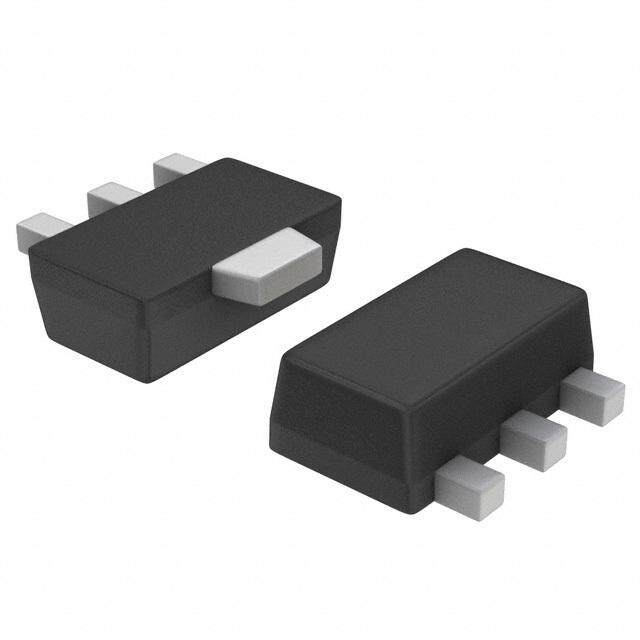
| 产品图片 |
|
| rohs | 符合RoHS无铅 / 符合限制有害物质指令(RoHS)规范要求 |
| 产品系列 | 电源管理 IC,低压差稳压器,Micrel MIC37252WU- |
| 数据手册 | |
| 产品型号 | MIC37252WU |
| PCN组件/产地 | |
| 产品目录页面 | |
| 产品种类 | 低压差稳压器 |
| 供应商器件封装 | TO-263-5 |
| 其它名称 | 576-1764-5 |
| 包装 | 管件 |
| 参考电压 | 1.24 V |
| 商标 | Micrel |
| 回动电压—最大值 | 1 V |
| 安装类型 | 表面贴装 |
| 安装风格 | SMD/SMT |
| 封装 | Tube |
| 封装/外壳 | TO-263-6,D²Pak(5 引线+接片),TO-263BA |
| 封装/箱体 | TO-263-5 |
| 工作温度 | -40°C ~ 125°C |
| 工厂包装数量 | 50 |
| 最大工作温度 | + 125 C |
| 最大输入电压 | 6 V |
| 最小工作温度 | - 40 C |
| 标准包装 | 50 |
| 电压-跌落(典型值) | 0.55V @ 2.5A |
| 电压-输入 | 3 V ~ 6 V |
| 电压-输出 | 1.24 V ~ 5.5 V |
| 电流-输出 | 2.5A |
| 电流-限制(最小值) | - |
| 稳压器拓扑 | 正,可调式 |
| 稳压器数 | 1 |
| 系列 | MIC37252 |
| 线路调整率 | 0.02 % |
| 负载调节 | 0.2 % |
| 输入偏压电流—最大 | 120 nA |
| 输出电压 | 1.24 V to 5.5 V |
| 输出电压容差 | 2 % |
| 输出电流 | 2.5 A |
| 输出端数量 | 1 Output |
| 输出类型 | Adjustable |


- 商务部:美国ITC正式对集成电路等产品启动337调查
- 曝三星4nm工艺存在良率问题 高通将骁龙8 Gen1或转产台积电
- 太阳诱电将投资9.5亿元在常州建新厂生产MLCC 预计2023年完工
- 英特尔发布欧洲新工厂建设计划 深化IDM 2.0 战略
- 台积电先进制程称霸业界 有大客户加持明年业绩稳了
- 达到5530亿美元!SIA预计今年全球半导体销售额将创下新高
- 英特尔拟将自动驾驶子公司Mobileye上市 估值或超500亿美元
- 三星加码芯片和SET,合并消费电子和移动部门,撤换高东真等 CEO
- 三星电子宣布重大人事变动 还合并消费电子和移动部门
- 海关总署:前11个月进口集成电路产品价值2.52万亿元 增长14.8%


PDF Datasheet 数据手册内容提取
MIC37252 2.5A, Low Voltage µCap LDO Regulator General Description Features The Micrel MIC37252 is a 2.5A low-dropout linear voltage • 2.5A minimum guaranteed output current regulator that provides a low voltage, high current output • Ideal for 3.3V to 1.8V conversion with a minimum of external components. It offers high • Stable with ceramic or tantalum capacitor precision, low dropout and low ground current. • ±2.0% initial output tolerance The MIC37252 operates from an input voltage of 3.0V • Dropout voltage = 550mV @ 2.5A to6.0V. It is designed to drive digital circuits requiring low • Excellent line and load regulation specifications voltage at high currents (i.e., PLDs, DSP, microcontroller, • Logic controlled shutdown etc.). It is available in an adjustable output voltage capable of 1.24V to 5.5V. • Thermal shutdown and current limit protection • Reverse-leakage protection Features of the MIC37252 LDO include thermal and • S-Pak and TO-263 packages current limit protection, and reverse current and reverse battery protection. Applications Junction temperature range of the MIC37252 is from –40°C to +125°C. • LDO linear regulator for low-voltage digital IC • PC add-in cards For higher currents see the MIC3730x family of LDOs. • High efficiency linear power supplies • SMPS post regulator • Battery charger ____________________________________________________________________________________________________________ Typical Application Adjustable Regulator SuperSwitcher and Super ßeta PNP are trademarks of Micrel, Inc. Micrel Inc. • 2180 Fortune Drive • San Jose, CA 95131 • USA • tel +1 (408) 944-0800 • fax + 1 (408) 474-1000 • http://www.micrel.com February 2006 M9999-021606 (408) 955-1690
Micrel, Inc. MIC37252 Ordering Information Part Number Output Junction Voltage* Package Current Temperature Range Standard RoHS Compliant** MIC37252BR MIC37252WR 2.5A Adj. –40° to +125°C S-Pak-5 MIC37252BU MIC37252WU 2.5A Adj. –40° to +125°C TO-263-5 *For other voltages, please contact Micrel Marketing. **RoHS compliant with “high melting solder” exemption. Pin Configuration S-PAK5 (R) TO-263 (U) Pin Description Pin Number Pin Name Pin Function 1 EN Enable (Input): CMOS compatible input. Logic high = enable, logic low = shutdown. 2 VIN Input voltage which supplies current to the output power device. 3 GND Ground (TAB is connected to ground on S-Pak). 4 VOUT Regulator Output. 5 ADJ Adjustable regulator feedback input. Connect to resistor voltage divider. February 2006 2 M9999-021606 (408) 955-1690
Micrel, Inc. MIC37252 Absolute Maximum Ratings(1) Operating Ratings(2) Supply Voltage (V )......................................................6.5V Supply voltage (V ).........................................3.0V to 6.0V IN IN Enable Input Voltage (V )............................................6.5V Enable Input Voltage (V )..................................0V to 6.0V EN EN Power Dissipation.....................................Internally Limited Junction Temperature Range.............–40°C ≤ T ≤ +125°C J Junction Temperature.........................–40°C ≤ T ≤ +125°C Maximum Power Dissipation(4) J Storage Temperature..........................–65°C ≤ T ≤ +150°C Package Thermal Resistance J Lead Temperature (soldering, 5sec.).........................260°C S-Pak (θ )..........................................................2°C/W JC EDS(3) TO-263-5 (θ ).....................................................2°C/W JC Electrical Characteristics(5) T = 25°C with V = V + 1V; V = V ; I = 10mA, bold values indicate –40°C< T < +125°C, unless otherwise noted. A IN OUT EN IN L J Parameter Condition Min Typ Max Units Output Voltage Accuracy I = 10mA -2 +2 % L 10mA < I < I , V + 1 ≤ V ≤ 6V -3 +3 % OUT L(max) OUT IN Output Voltage Line Regulation V = V + 1.0V to 6.0V, I = 10mA 0.02 0.5 % IN OUT L Output Voltage Load Regulation I = 10mA to 2.5A 0.2 1 % L V – V ; Dropout Voltage, I = 1.5A 400 500 mV IN OUT L Note 6 I = 2.5A 550 1000 mV L Ground Pin Current, Note 7 I = 2.5A 40 60 mA L Ground Pin Current in Shutdown V ≤ 0.5V, V = V + 1V 1.0 µA IL IN OUT Current Limit V = 0; V = 3.3V 3 A OUT IN Start-up Time V = V , I = 10mA, C = 47µF 150 250 µs EN IN OUT OUT Enable Input Enable Input Threshold Regulator enable 2.25 V Regulator shutdown 0.8 V Enable Pin Input Current V ≤ 0.8V (Regulator shutdown) 2 µA IL 4 µA V ≥ 2.25V (Regulator enable) 1 10 30 µA IH Reference Voltage 1.215 1.240 1.265 V 1.202 1.277 V Adjust Pin Bias Current 40 80 nA 120 nA Notes: 1. Exceeding the absolute maximum rating may damage the device. 2. The device is not guaranteed to function outside its operating rating. 3. Device is ESD sensitive. Handling precautions recommended. 4. P = T – T ) / θ , where θ , depends upon the printed circuit layout. See “Applications Information.” D(max) J(max) A JA JA 5. Specification for packaged product only 6. V = V – V when V decreased to 98% of its nominal output voltage with V = V + 1V. For output voltages below 2V, dropout voltage DO IN OUT OUT IN OUT specification does not apply due to a minimum input operating voltage of 3V 7. I is the quiescent current. I = I + I . GND IN GND OUT February 2006 3 M9999-021606 (408) 955-1690
Micrel, Inc. MIC37252 Typical Characteristics PSRR PSRR Dropout Voltage 70 70 600 V = 3.3V 60100mA 60 100mA )Vm500 OUT 1A 1A ( 50 50 E 2.5A 2.5A G400 )Bd(S40 )Bd(R40 ATLO300 S30 R30 V R S T P P U200 20 C = 100µF Ceramic 20 C = 47µF O OUT OUT P 10 VIN = 3.3V 10 VIN = 3.3V OR100 V = 1.8V V = 1.8V D OUT OUT 0 0 0 1 10 100 1k 10k 100k 1M 1 10 100 1k 10k 100k 1M 0 0.5 1 1.5 2 2.5 FREQUENCY (Hz) FREQUENCY (Hz) OUTPUT CURRENT (A) Dropout Output Voltage Enable Pin Current vs. Temperature vs. Temperature vs. Temperature 600 1.85 18 )Vm500 )V11..8834 )A16 100mA Load (EGATLOVTUOPORD123400000000 32..35VAO lUoTad (EGATLOVTUPTUO1111111.......77778886789012 (TNERRUCELBANEµ1112468024 0-40-20 0 20 40 60 80100120 1.75-40-20 0 20 40 60 80100120 0-40-20 0 20 40 60 80100120 TEMPERATURE °(C) TEMPERATURE °(C) TEMPERATURE °(C) Short Circuit Current Ground Current Ground Current vs. Temperature vs. Supply Voltage vs. Temperature 4 50 50 )A(T3.5 )A45 )A45 2.5A Load N m40 m40 ER 3 (T35 2.5A (T35 R N N UC2.5 ER30 ER30 TIUCR1.25 RUCD2205 RUCD2205 ICTR 1 VOUT = 0V NUOR1105 1.5A NUOR1105 1A Load OH0.5 VIN = 4.3V G 5 0.5A G 510mA Load S 0 0 0 -40-20 0 20 40 60 80100120 0 1 2 3 4 5 -40-20 0 20 40 60 80100120 TEMPERATURE T (°C) SUPPLY VOLTAGE (V) TEMPERATURE °(C) J Ground Current Output Voltage vs. Output Current vs. Load Current Dropout Characteristics 50 2.510 2.0 )Am 4405 )V 22..550068 )V11..68 0.5A ( ( ( TN 35 EG 2.504 EG1.4 1.5A ER 30 AT 2.502 AT1.2 RU 25 LO 2.500 LO1.0 C V V DNUOR 112050 TUPTUO 222...444999468 TUPTUO000...468 2.5A G 5 2.4922.5V 0.2 OUT 0 2.490 0.0 0 0.5 1 1.5 2 2.5 0 0.5 1 1.5 2 2.5 0 1 2 3 4 OUTPUT CURRENT (A) OUTPUT CURRENT (A) SUPPLY VOLTAGE (V) February 2006 4 M9999-021606 (408) 955-1690
Micrel, Inc. MIC37252 Functional Characteristics LoadTransient Response LoadTransient Response E V = 3.3V G V = 3.3V EGATLOVTUPTU).vid/Vm001( VCIOONUUTT == 14.78µVF ATLOVTUPTUO).vid/Vm002( VCIOONUUTT == 14.78µVF O T NE 2.5A TNER 2A RRUCTUP).vid/A1( RU).v 10mA TU 10mA Cid O TUP/A1( T U O TIME (400µs/div.) TIME (400µs/div.) LineTransient Response E G A TL).v Oid V/V Tm U0 P2 T( U O 5V 3.3V E G A TL).v Oid V/V T2 U( P N I TIME (100µs/div.) February 2006 5 M9999-021606 (408) 955-1690
Micrel, Inc. MIC37252 Application Information applications where the minimum input voltage is known and is large compared with the dropout voltage. Use a The MIC37252 is a high-performance low-dropout series input resistor to drop excessive voltage and voltage regulator suitable for moderate to high-current distribute the heat between this resistor and the regulator applications. Its 550mV dropout voltage at full regulator. The low dropout properties of Micrel Super load makes it especially valuable in battery-powered βeta PNP® regulators allow significant reductions in systems and as high-efficiency noise filters in post- regulator power dissipation and the associated heat sink regulator applications. Unlike older NPN-pass transistor without compromising performance. When this technique designs, where the minimum dropout voltage is limited is employed, a capacitor of at least 1.0µF is needed by the base-to-emitter voltage drop and collector-to- directly between the input and regulator ground. Refer to emitter saturation voltage, dropout performance of the Application Note 9 for further details and examples on PNP output of these devices is limited only by the low thermal design and heat sink applications. V saturation voltage. CE Output Capacitor A trade off for the low dropout voltage is a varying base The MIC37252 requires an output capacitor for stable drive requirement. Micrel’s Super βeta PNP® process operation. As a µCap LDO, the MIC37252 can operate reduces this drive requirement to only 2% to 5% of the with ceramic output capacitors as long as the amount of load current. capacitance is 47µF or greater. For values of output The MIC37252 regulator is fully protected from damage capacitance lower than 47µF, the recommended ESR due to fault conditions. Current limiting is provided. This range is 200mΩ to 2Ω. The minimum value of output capacitance recommended for theMIC37252 is 10µF. limiting is linear; output current during overload conditions is constant. Thermal shutdown disables the For 47µF or greater the ESR range recommended is device when the die temperature exceeds the maximum less than1Ω. Ultra-low ESR, ceramic capacitors are safe operating temperature. Transient protection allows recommended for output capacitance of 47µF or greater device (and load) survival even when the input voltage to help improve transient response and noise reduction spikes above and below nominal. The output structure of at high frequency. X7R/X5R dielectric-type ceramic these regulators allows voltages in excess of the desired capacitors are recommended because of their output voltage to be applied without reverse current flow. temperature performance. X7R-type capacitors change capacitance by 15% over their operating temperature Thermal Design range and are the most stable type of ceramic Linear regulators are simple to use. The most capacitors. Z5U and Y5V dielectric capacitors change complicated design parameters to consider are thermal value by as much as 50% and 60% respectively over characteristics. Thermal design requires the following their operating temperature ranges. To use a ceramic application-specific parameters: chip capacitor withY5V dielectric, the value must be • Maximum ambient temperature (TA) much higher than an X7Rceramic capacitor to ensure • Output current (I ) the same minimum capacitance over the equivalent OUT operating temperature range. The MIC37252 has • Output voltage (V ) OUT excellent transient response to variations in input voltage • Input voltage (VIN) and load current. The device has been designed to • Ground current (I ) respond quickly to load current variations and input GND voltage variations. Large output capacitors are not First, calculate the power dissipation of the regulator required to obtain this performance. A standard 47µF from these numbers and the device parameters from this output capacitor is all that is required. Larger values help datasheet. to improve performance even further. P = (V – V ) I + V I Input Capacitor D IN OUT OUT IN GND An input capacitor of 1.0µF or greater is recommended Where the ground current is approximated by using when the device is more than 4 inches away from the numbers from the “Electrical Characteristics” or “Typical bulk supply capacitance, or when the supply is a battery. Characteristics.” Then the heat sink thermal resistance is Small, surface-mount chip capacitors can be used for determined with this formula: the bypassing. The capacitor should be place within 1” of θ = ((T – T )/ P ) – (θ + θ ) the device for optimal performance. Larger values will SA J(MAX) A D JC CS help to improve ripple rejection by bypassing the input to Where T ≤ 125°C and θ is between 0°C and the regulator, further improving the integrity of the output J(MAX) CS 2°C/W. The heat sink may be significantly reduced in voltage. February 2006 6 M9999-021606 (408) 955-1690
Micrel, Inc. MIC37252 Transient Response and 5V to 3.3V or 3.3V to input is TTL/CMOS compatible for simple logic interface, 1.8VConversions but can be connected to up to VIN. When enabled, it draws approximately 15µA. The MIC37252 has excellent transient response to variations in input voltage and load current. The device Adjustable Regulator Design has been designed to respond quickly to load current variations and input voltage variations. Large output capacitors are not required to obtain this performance. A standard 10µF output capacitor, preferably tantalum, is all that is required. Larger values help to improve performance even further. By virtue of its low dropout voltage, this device does not saturate into dropout as readily as similar NPN-based designs. When converting from 3.3V to 1.8V, the NPN- Figure 2. Adjustable Regulator with Resistors based regulators are already operating in dropout, with The MIC37252 allows programming of the output voltage typical dropout requirements of 2V or greater. To convert anywhere between 1.24V and the 5.5V maximum down to1.8V without operating in dropout, NPN-based operating rating of the family. Two resistors are used. regulators require an input voltage of 3.8V at the very Resistors values are recommended to be less than 10kΩ least. The MIC37252 regulator will provide excellent in value to improve stability. The resistor values can be performance with an input as low as 3.0V. This gives the sized to draw the mini-mum load current for this device. PNP-based regulators a distinct advantage over older The resistor values are calculated by: NPN-based linear regulators. ⎛V ⎞ Minimum Load Current R1=R2⎜ OUT −1⎟ ⎜ ⎟ The MIC37252 regulator is specified between finite ⎝1.240 ⎠ loads. If the output current is too small, leakage currents dominate and the output voltage rises. A 10mA minimum Where VOUT is the desired output voltage. Figure 2 load current is necessary for proper operation. shows component definition. Applications with widely varying load currents may scale the resistors to draw the Enable Input minimum load current required for proper operation (see above). The MIC37252 also features an enable input for on/off control of the device. Its shutdown state draws “zero” current (only microamperes of leakage). The enable February 2006 7 M9999-021606 (408) 955-1690
Micrel, Inc. MIC37252 Package Information 5-Pin S-PAK (R) θ4 θ1 θ2 θ1 θ3 θ1 θ2 θ3 θ4 θ1 5-Pin TO-263 (U) MICREL, INC. 2180 FORTUNE DRIVE SAN JOSE, CA 95131 USA TEL +1 (408) 944-0800 FAX +1 (408) 474-1000 WEB http:/www.micrel.com The information furnished by Micrel in this data sheet is believed to be accurate and reliable. However, no responsibility is assumed by Micrel for its use. Micrel reserves the right to change circuitry and specifications at any time without notification to the customer. Micrel Products are not designed or authorized for use as components in life support appliances, devices or systems where malfunction of a product can reasonably be expected to result in personal injury. Life support devices or systems are devices or systems that (a) are intended for surgical implant into the body or (b) support or sustain life, and whose failure to perform can be reasonably expected to result in a significant injury to the user. A Purchaser’s use or sale of Micrel Products for use in life support appliances, devices or systems is a Purchaser’s own risk and Purchaser agrees to fully indemnify Micrel for any damages resulting from such use or sale. © 2002 Micrel, Incorporated. February 2006 8 M9999-021606 (408) 955-1690
Mouser Electronics Authorized Distributor Click to View Pricing, Inventory, Delivery & Lifecycle Information: M icrochip: MIC37252WR MIC37252WU MIC37252WR-TR MIC37252WU-TR