ICGOO在线商城 > MIC2571-1YMM
 Datasheet下载
- 型号: MIC2571-1YMM
- 制造商: Micrel
- 库位|库存: xxxx|xxxx
- 要求:
| 数量阶梯 | 香港交货 | 国内含税 |
| +xxxx | $xxxx | ¥xxxx |
查看当月历史价格
查看今年历史价格
MIC2571-1YMM产品简介:
ICGOO电子元器件商城为您提供MIC2571-1YMM由Micrel设计生产,在icgoo商城现货销售,并且可以通过原厂、代理商等渠道进行代购。 提供MIC2571-1YMM价格参考¥询价-¥询价以及MicrelMIC2571-1YMM封装/规格参数等产品信息。 你可以下载MIC2571-1YMM参考资料、Datasheet数据手册功能说明书, 资料中有MIC2571-1YMM详细功能的应用电路图电压和使用方法及教程。
| 参数 | 数值 |
| 产品目录 | 集成电路 (IC)半导体 |
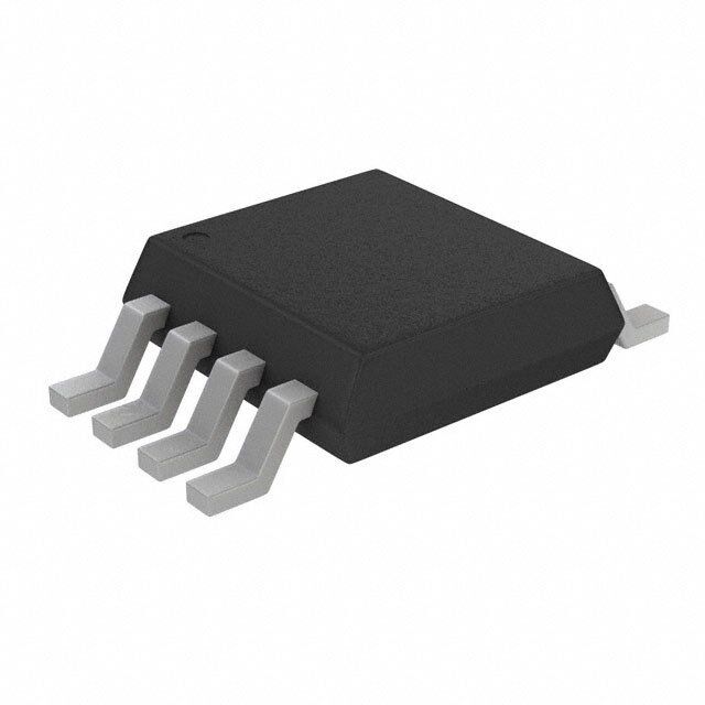
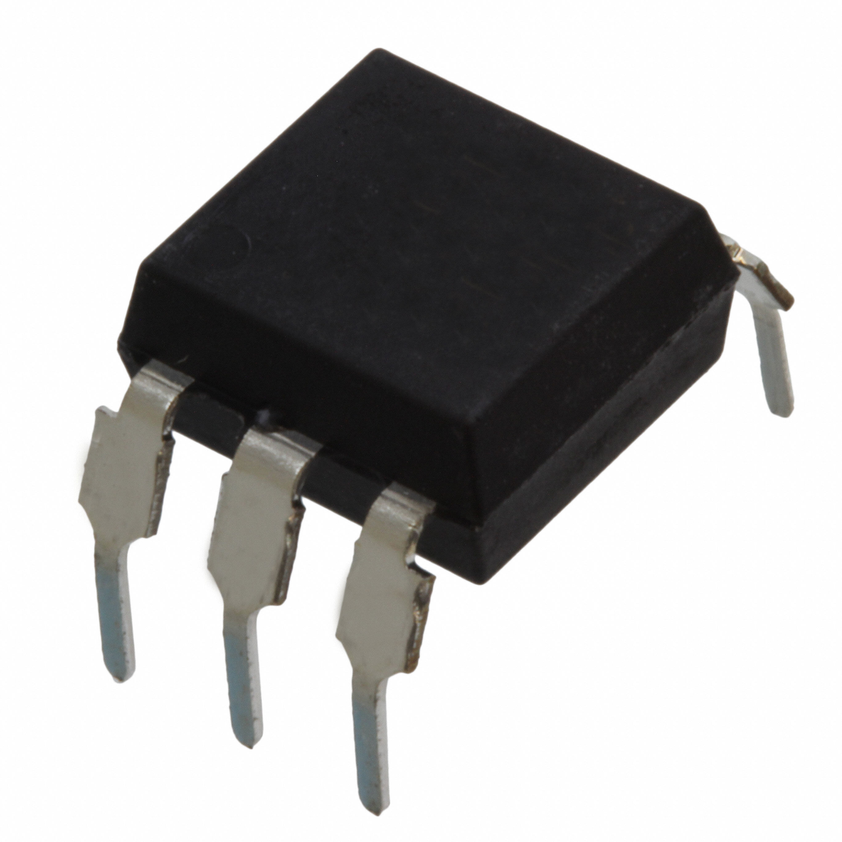
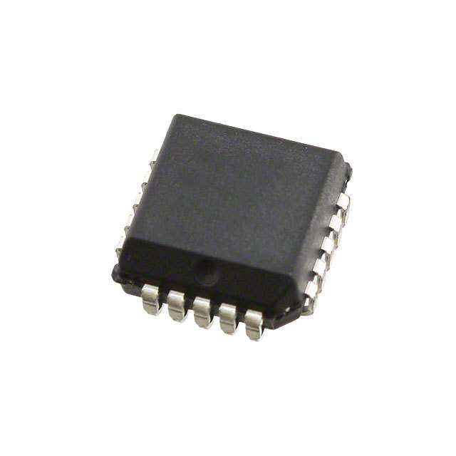
| 描述 | IC REG BOOST 2.85V/3.3V/5V 8MSOP稳压器—开关式稳压器 One Cell Boost Regulator (Lead Free) |
| 产品分类 | |
| 品牌 | Micrel |
| 产品手册 | |
| 产品图片 |
|
| rohs | 符合RoHS无铅 / 符合限制有害物质指令(RoHS)规范要求 |
| 产品系列 | 电源管理 IC,稳压器—开关式稳压器,Micrel MIC2571-1YMM- |
| 数据手册 | |
| 产品型号 | MIC2571-1YMM |
| PCN组件/产地 | |
| PWM类型 | - |
| 产品目录页面 | |
| 产品种类 | 稳压器—开关式稳压器 |
| 供应商器件封装 | 8-MSOP |
| 其它名称 | 576-2192 |
| 包装 | 管件 |
| 同步整流器 | 无 |
| 商标 | Micrel |
| 安装类型 | 表面贴装 |
| 安装风格 | SMD/SMT |
| 封装 | Tube |
| 封装/外壳 | 8-TSSOP,8-MSOP(0.118",3.00mm 宽) |
| 封装/箱体 | MSOP-8 |
| 工作温度 | -40°C ~ 85°C |
| 工厂包装数量 | 100 |
| 开关频率 | 20 kHz |
| 拓扑结构 | Boost |
| 最大工作温度 | + 85 C |
| 最大输入电压 | 15 V |
| 最小工作温度 | - 40 C |
| 最小输入电压 | 0.9 V |
| 标准包装 | 100 |
| 电压-输入 | 0.9 V ~ 15 V |
| 电压-输出 | 2.85V,3.3V,5V |
| 电流-输出 | 1A |
| 电源电流 | 120 uA |
| 类型 | Single-Cell Switching Regulators |
| 系列 | MIC2571 |
| 输出数 | 1 |
| 输出电压 | 2.85 V, 3.3 V, 5 V |
| 输出电流 | 1 A |
| 输出端数量 | 1 Output |
| 输出类型 | 固定 |
| 频率-开关 | 20kHz |


- 商务部:美国ITC正式对集成电路等产品启动337调查
- 曝三星4nm工艺存在良率问题 高通将骁龙8 Gen1或转产台积电
- 太阳诱电将投资9.5亿元在常州建新厂生产MLCC 预计2023年完工
- 英特尔发布欧洲新工厂建设计划 深化IDM 2.0 战略
- 台积电先进制程称霸业界 有大客户加持明年业绩稳了
- 达到5530亿美元!SIA预计今年全球半导体销售额将创下新高
- 英特尔拟将自动驾驶子公司Mobileye上市 估值或超500亿美元
- 三星加码芯片和SET,合并消费电子和移动部门,撤换高东真等 CEO
- 三星电子宣布重大人事变动 还合并消费电子和移动部门
- 海关总署:前11个月进口集成电路产品价值2.52万亿元 增长14.8%


PDF Datasheet 数据手册内容提取
MIC2571 Micrel MIC2571 Single-Cell Switching Regulator Final Information General Description Features Micrel’s MIC2571 is a micropower boost switching regulator • Operates from a single-cell supply that operates from one alkaline, nickel-metal-hydride cell, or 0.9V to 15V operation lithium cell. • 120µA typical quiescent current The MIC2571 accepts a positive input voltage between 0.9V • Complete regulator fits 0.3 in2 area and 15V. Its typical no-load supply current is 120µA. • 2.85V/3.3V/5V selectable output voltage (MIC2571-1) • Adjustable output up to 36V (MIC2571-2) The MIC2571 is available in selectable fixed output or adjust- • 1A current limited pass element able output versions. The MIC2571-1 can be configured for • Frequency synchronization input 2.85V, 3.3V, or 5V by connecting one of three separate • 8-lead MSOP package feedback pins to the output. The MIC2571-2 can be config- ured for an output voltage ranging between its input voltage Applications and 36V, using an external resistor network. The MIC2571 has a fixed switching frequency of 20kHz. An • Pagers external SYNC connection allows the switching frequency to • LCD bias generator be synchronized to an external signal. • Battery-powered, hand-held instruments The MIC2571 requires only four components (diode, induc- • Palmtop computers tor, input capacitor and output capacitor) to implement a • Remote controls boost regulator. A complete regulator can be constructed in • Detectors a 0.3 in2 area. • Battery Backup Supplies All versions are available in an 8-lead MSOP with an operat- ing range from –40°C to +85°. Typical Applications L1 D1 L1 D1 150µH MBR0530 150µH MBR0530 5V/5mA 3.3V/8mA 8 8 IN IN SW 1 SW 1 1V to1.5V C471µ*F 2.85V 6 1V to1.5V C471µ*F 2.85V 6 1 Cell 16V MIC2571-1 3.3V 5 1 Cell 16V MIC2571-1 3.3V 5 5V 4 C2 5V 4 C2 SYNC GND 47µF SYNC GND 47µF 7 2 16V 7 2 16V * Needed if battery is ≥ 4" from MIC2571 * Needed if battery is ≥ 4" from MIC2571 Circuit size < 0.3 in2 excluding C1 Circuit size < 0.3 in2 excluding C1 Single-Cell to 5V DC-to-DC Converter Single-Cell to 3.3V DC-to-DC Converter Micrel, Inc. • 1849 Fortune Drive • San Jose, CA 95131 • USA • tel + 1 (408) 944-0800 • fax + 1 (408) 944-0970 • http://www.micrel.com 1997 1 MIC2571
MIC2571 Micrel Ordering Information Part Number Temperature Range Voltage Frequency Package MIC2571-1BMM –40°C to +85°C Selectable* 20kHz 8-lead MSOP MIC2571-2BMM –40°C to +85°C Adjustable 20kHz 8-lead MSOP * Externally selectable for 2.85V, 3.3V, or 5V Pin Configuration MIC2571-1 MIC2571-2 SW 1 8 IN SW 1 8 IN GND 2 7 SYNC GND 2 7 SYNC NC 3 6 2.85V NC 3 6 FB 5V 4 5 3.3V NC 4 5 NC Selectable Voltage Adjustable Voltage 20kHz Frequency 20kHz Frequency 8-Lead MSOP (MM) Pin Description Pin No. (Version†) Pin Name Pin Function 1 SW Switch: NPN output switch transistor collector. 2 GND Power Ground: NPN output switch transistor emitter. 3 NC Not internally connected. 4 (-1) 5V 5V Feedback (Input): Fixed 5V feedback to internal resistive divider. 4 (-2) NC Not internally connected. 5 (-1) 3.3V 3.3V Feedback (Input): Fixed 3.3V feedback to internal resistive divider. 5 (-2) NC Not internally connected. 6 (-1) 2.85V 2.85V Feedback (Input): Fixed 2.85V feedback to internal resistive divider. 6 (-2) FB Feedback (Input): 0.22V feedback from external voltage divider network. 7 SYNC Synchronization (Input): Oscillator start timing. Oscillator synchronizes to falling edge of sync signal. 8 IN Supply (Input): Positive supply voltage input. † Example: (-1) indicates the pin description is applicable to the MIC2571-1 only. MIC2571 2 1997
MIC2571 Micrel Absolute Maximum Ratings Operating Ratings Supply Voltage (V ) .....................................................18V Supply Voltage (V ) ....................................+0.9V to +15V IN IN Switch Voltage (V )....................................................36V Ambient Operating Temperature (T )........–40°C to +85°C SW A Switch Current (I ) .......................................................1A Junction Temperature (T ).......................–40°C to +125°C SW J Sync Voltage (V ).................................... –0.3V to 15V MSOP Thermal Resistance (θ )..........................240°C/W SYNC JA Storage Temperature (T ) .......................–65°C to +150°C A MSOP Power Dissipation (P )................................250mW D Electrical Characteristics V = 1.5V; T = 25°C,bold indicates –40°C≤ T ≤ 85°C; unless noted IN A A Parameter Condition Min Typ Max Units Input Voltage Startup guaranteed, I = 100mA 15 V SW 0.9 V Quiescent Current Output switch off 120 µA Fixed Feedback Voltage MIC2571-1; V = V , I = 100mA 2.7 2.85 3.0 V 2.85V pin OUT SW MIC2571-1; V = V , I = 100mA 3.14 3.30 3.47 V 3.3V pin OUT SW MIC2571-1; V = V , I = 100mA 4.75 5.00 5.25 V 5V pin OUT SW Reference Voltage MIC2571-2, [adj. voltage versions], I = 100mA, Note 1 208 220 232 mV SW Comparator Hysteresis MIC2571-2, [adj. voltage versions] 6 mV Output Hysteresis MIC2571-1; V = V , I = 100mA 65 mV 2.85V pin OUT SW MIC2571-1; V = V , I = 100mA 75 mV 3.3V pin OUT SW MIC2571-1; V = V , I = 100mA 120 mV 5V pin OUT SW Feedback Current MIC2571-1; V = V 4.5 µA 2.85V pin OUT MIC2571-1; V = V 4.5 µA 3.3V pin OUT MIC2571-1; V = V 4.5 µA 5V pin OUT MIC2571-2, [adj. voltage versions]; V = 0V 25 nA FB Reference Line Regulation 1.0V ≤ V ≤ 12V 0.35 %/V IN Switch Saturation Voltage V = 1.0V, I = 200mA 200 mV IN SW V = 1.2V, I = 600mA 400 mV IN SW V = 1.5V, I = 800mA 500 mV IN SW Switch Leakage Current Output switch off, V = 36V 1 µA SW Oscillator Frequency MIC2571-1, -2; I = 100mA 20 kHz SW Maximum Output Voltage 36 V Sync Threshold Voltage 0.7 V Switch On Time 35 µs Currrent Limit 1.1 A Duty Cycle V < V , I = 100mA 67 % FB REF SW General Note: Devices are ESD protected; however, handling precautions are recommended. Note 1: Measured using comparator trip point. 1997 3 MIC2571
MIC2571 Micrel Typical Characteristics Switch Saturation Voltage Switch Saturation Voltage Switch Saturation Voltage 1.0 1.0 1.0 T = –40°C 1.4V 1.3V 1.4V 1.3V A NT (A)0.8 NT (A)0.8 TA = 25°C 1.2V NT (A)0.8 TA = 85°C 1.11V.2V RE0.6 1.4V RE0.6 1.1V RE0.6 UR 1.3V UR UR 1.0V C C C H 0.4 1.2V H 0.4 1.0V H 0.4 V = 0.9V C C C IN T 1.1V T T WI0.2 WI0.2 V = 0.9V WI0.2 S S IN S V = 1.0V IN 0 0 0 0 0.2 0.4 0.6 0.8 1.0 0 0.2 0.4 0.6 0.8 1.0 0 0.2 0.4 0.6 0.8 1.0 SWITCH VOLTAGE (V) SWITCH VOLTAGE (V) SWITCH VOLTAGE (V) Oscillator Frequency Oscillator Duty Cycle Quiescent Current vs. Temperature vs. Temperature vs. Temperature 30 75 200 NCY (kHz)25 VISIWN == 11.050VmA LE (%)6750 VISIWN == 11.050VmA µRRENT (A)115705 VIN = 1.5V E C U U Y C125 OSC. FREQ20 DUTY C5650 UIESCENT 10705 Q 15 50 50 -60 -30 0 30 60 90 120 150 -60 -30 0 30 60 90 120 150 -60 -30 0 30 60 90 120 150 TEMPERATURE (°C) TEMPERATURE (°C) TEMPERATURE (°C) Feedback Current Feedback Current Quiescent Current vs. Temperature vs. Temperature vs. Supply Voltage 10 50 200 µNT (A) 8 VMIINC =2 517.51V-1 NT (nA)40 MVIINC =2 527.51V-2 µNT (A)115705 –40°C +25°C CURRE 6 CURRE30 CURRE110205 +85°C EEDBACK 24 EEDBACK 1200 UIESCENT 257505 F F Q 0 0 0 -60 -30 0 30 60 90 120 150 -60 -30 0 30 60 90 120 150 0 2 4 6 8 10 TEMPERATURE (°C) TEMPERATURE (°C) SUPPLY VOLTAGE (V) Output Current Limit Switch Leakage Current Output Hysteresis vs. Temperature vs. Temperature vs. Temperature 1.75 A)1000 150 n T (A)11..2550 RRENT ( 100 SIS (mV)110205 5V URRENT LIMI001...570050 LEAKAGE CU 110 UT HYSTERE 5705 VOUT3 .=3 V2.85V C0.25 CH 0.1 UTP 25 WIT O 0-60 -30 0 30 60 90 120 150 S0.01-60 -30 0 30 60 90 120 150 0-60 -30 0 30 60 90 120 150 TEMPERATURE (°C) TEMPERATURE (°C) TEMPERATURE (°C) MIC2571 4 1997
MIC2571 Micrel Block Diagrams V V BATT OUT IN SYNC MIC2571-1 Oscillator 0.22V Reference Driver SW 5V 3.3V 2.85V GND Selectable Voltage Version with External Components V V BATT OUT IN SYNC MIC2571-2 Oscillator 0.22V Reference Driver SW FB GND Adjustable Voltage Version with External Components 1997 5 MIC2571
MIC2571 Micrel Functional Description The MIC2571 switch-mode power supply (SMPS) is a gated 5V ye V oscillator architecture designed to operate from an input plag IN voltage as low as 0.9V and provide a high-efficiency fixed or SupVolt 0V adjustable regulated output voltage. One advantage of this aothruecthpreiutbet ycv togulrrtaeega isetl ty hi sar eat tdbhuoecv oienu gtthp qeuu tf sieewesdictbcehan ctis kc d cuisorramebnpleta draa wntdoh re itmnheprevreoshrv tionhlgde PeakCurrent I0PmEAAK efficiency, especially at low output currents. utge Refer to the Block Diagrams for the following discription of pa 5V typical gated oscillator boost regulator function. OutVolt Time The bandgap reference provides a constant 0.22V over a wide range of input voltage and junction temperature. The comparator senses the output voltage through an internal or Figure 1. Typical Boost Regulator Waveforms external resistor divider and compares it to the bandgap Synchronization reference voltage. The SYNC pin is used to synchronize the MIC2571 to an When the voltage at the inverting input of the comparator is external oscillator or clock signal. This can reduce system below 0.22V, the comparator output is high and the output of noise by correlating switching noise with a known system the oscillator is allowed to pass through the AND gate to the frequency. When not in use, the SYNC pin should be output driver and output switch. The output switch then turns grounded to prevent spurious circuit operation. A falling edge on and off storing energy in the inductor. When the output at the SYNC input triggers a one-shot pulse which resets the switch is on (low) energy is stored in the inductor; when the oscillator. It is possible to use the SYNC pin to generate switch is off (high) the stored energy is dumped into the output oscillator duty cycles from approximately 20% up to the capacitor which causes the output voltage to rise. nominal duty cycle. When the output voltage is high enough to cause the com- Current Limit parator output to be low (inverting input voltage is above Current limit for the MIC2571 is internally set with a resistor. 0.22V) the AND gate is disabled and the output switch It functions by modifying the oscillator duty cycle and fre- remains off (high). The output switch remains disabled until quency. When current exceeds 1.2A, the duty cycle is the output voltage falls low enough to cause the comparator reduced (switch on-time is reduced, off-time is unaffected) output to go high. and the corresponding frequency is increased. In this way There is about 6mV of hysteresis built into the comparator to less time is available for the inductor current to build up while prevent jitter about the switch point. Due to the gain of the maintaining the same discharge time. The onset of current feedback resistor divider the voltage at V experiences OUT limit is soft rather than abrupt but sufficient to protect the about 120mV of hysteresis for a 5V output. inductor and output switch from damage. Certain combina- Appications Information tions of input voltage, output voltage and load current can cause the inductor to go into a continuous mode of operation. Oscillator Duty Cycle and Frequency This is what happens when the inductor current can not fall to The oscillator duty cycle is set to 67% which is optimized to zero and occurs when: provide maximum load current for output voltages approxi- V + V – V mately 3× larger than the input voltage. Other output voltages duty cycle≤ OUT DIODE IN are also easily generated but at a small cost in efficiency. The VOUT + VDIODE – VSAT fixed oscillator frequency (options -1 and -2) is set to 20kHz. Output Waveforms The voltage waveform seen at the collector of the output Current "ratchet" switch (SW pin) is either a continuous value equal to V or a IN without current limit switching waveform running at a frequency and duty cycle set by the oscillator. The continuous voltage equal to VIN ent Current limit threshold happens when the voltage at the output (VOUT) is high urr enough to cause the comparator to disable the AND gate. In or C Continuous current this state the output switch is off and no switching of the ct u inductor occurs. When V drops low enough to cause the d OUT In comparator output to change to the high state the output Discontinuous current switch is driven by the oscillator. See Figure 1 for typical voltage waveforms in a boost application. Time Figure 2. Current Limit Behavior MIC2571 6 1997
MIC2571 Micrel Figure 2 shows an example of inductor current in the continu- Capacitors ous mode with its associated change in oscillator frequency It is important to select high-quality, low ESR, filter capacitors and duty cycle. This situation is most likely to occur with for the output of the regulator circuit. High ESR in the output relatively small inductor values, large input voltage variations capacitor causes excessive ripple due to the voltage drop and output voltages which are less than ~3× the input voltage. across the ESR. A triangular current pulse with a peak of Selection of an inductor with a saturation threshold above 500mA into a 200mΩ ESR can cause 100mV of ripple at the 1.2A will insure that the system can withstand these condi- output due the capacitor only. Acceptable values of ESR are tions. typically in the 50mΩ range. Inexpensive aluminum electro- Inductors, Capacitors and Diodes lytic capacitors usually are the worst choice while tantalum The importance of choosing correct inductors, capacitors and capacitors are typically better. Figure 4 demonstrates the diodes can not be ignored. Poor choices for these compo- effect of capacitor ESR on output ripple voltage. nents can cause problems as severe as circuit failure or as subtle as poorer than expected efficiency. 5.25 ) V ( a. E G A nt T e L urr O5.00 C V or b. T ct U u P nd T I U O c. 4.75 0 500 1000 1500 Time TIME (µs) Figure 3. Inductor Current: a. Normal, Figure 4. Output Ripple b. Saturating and c. Excessive ESR Output Diode Inductors Finally, the output diode must be selected to have adequate Inductors must be selected such that they do not saturate reverse breakdown voltage and low forward voltage at the under maximum current conditions. When an inductor satu- application current. Schottky diodes typically meet these rates, its effective inductance drops rapidly and the current requirements. can suddenly jump to very high and destructive values. Standard silicon diodes have forward voltages which are too Figure 3 compares inductors with currents that are correct large except in extremely low power applications. They can and unacceptable due to core saturation. The inductors have also be very slow, especially those suited to power rectifica- the same nominal inductance but Figure 3b has a lower tion such as the 1N400x series, which affects efficiency. saturation threshold. Another consideration in the selection Inductor Behavior of inductors is the radiated energy. In general, toroids have the best radiation characteristics while bobbins have the The inductor is an energy storage and transfer device. Its worst. Some bobbins have caps or enclosures which signifi- behavior (neglecting series resistance) is described by the cantly reduce stray radiation. following equation: The last electrical characteristic of the inductor that must be V I = × t considered is ESR (equivalent series resistance). Figure 3c L shows the current waveform when ESR is excessive. The where: normal symptom of excessive ESR is reduced power transfer V = inductor voltage (V) efficiency. Note that inductor ESR can be used to the designers advantage as reverse battery protection (current L = inductor value (H) limit) for the case of relatively low output power one-cell t = time (s) designs. The potential for very large and destructive currents I = inductor current (A) exits if a battery in a one-cell application is inserted back- If a voltage is applied across an inductor (initial current is wards into the circuit. In some applications it is possible to zero) for a known time, the current flowing through the limit the current to a nondestructive (but still battery draining) inductor is a linear ramp starting at zero, reaching a maximum level by choosing a relatively high inductor ESR value which value at the end of the period. When the output switch is on, does not affect normal circuit performance. the voltage across the inductor is: V = V – V 1 IN SAT 1997 7 MIC2571
MIC2571 Micrel When the output switch turns off, the voltage across the Referring to Figure 1, it can be seen the peak input current will inductor changes sign and flies high in an attempt to maintain be twice the average input current. Rearranging the inductor a constant current. The inductor voltage will eventually be equation to solve for L: clamped to a diode drop above V . Therefore, when the OUT V output switch is off, the voltage across the inductor is: L = × t I 1 V = V + V – V 2 OUT DIODE IN V For normal operation the inductor current is a triangular L = IN(min) × t 2 × Average I 1 waveform which returns to zero current (discontinuous mode) IN(max) at each cycle. At the threshold between continuous and duty cycle discontinuous operation we can use the fact that I = I to get: 1 2 where t = 1 f V × t = V × t OSC 1 1 2 2 To illustrate the use of these equations a design example will V t 1 = 2 be given: V t 2 1 Assume: This relationship is useful for finding the desired oscillator MIC2571-1 (fixed oscillator) duty cycle based on input and output voltages. Since input V = 5V OUT voltages typically vary widely over the life of the battery, care I =5mA OUT(max) must be taken to consider the worst case voltage for each V = 1.0V parameter. For example, the worst case for t is when V is IN(min) 1 IN at its minimum value and the worst case for t is when V is efficiency = 75%. 2 IN at its maximum value (assuming that VOUT, VDIODE and VSAT 5V × 5mA do not change much). Average I = = 33.3mA IN(max) 1.0V × 0.75 To select an inductor for a particular application, the worst 1.0V × 0.7 case input and output conditions must be determined. Based L = on the worst case output current we can estimate efficiency 2 × 33.3mA × 20kHz and therefore the required input current. Remember that this L = 525µH is power conversion, so the worst case average input current Use the next lowest standard value of inductor and verify that will occur at maximum output current and minimum input it does not saturate at a current below about 75mA voltage. (< 2 × 33.3mA). V × I OUT OUT(max) Average I = IN(max) V × Efficiency IN(min) MIC2571 8 1997
MIC2571 Micrel Application Examples L1 D1 V OUT 150µH 5V/5mA MBR0530 8 IN 1 SW 1V to 1.5V C1* 1 Cell 47µF MIC2571 16V 5V 4 SYNC GND C2 7 2 47µF 16V * Needed if battery is more than 4" away from MIC2571 U1 Micrel MIC2571-1BMM C1 Sprague 594D476X0016C2T Tantalum ESR = 0.11Ω C2 Sprague 594D476X0016C2T Tantalum ESR = 0.11Ω D1 Motorola MBR0530T1 L1 Coilcraft DO1608C-154 DCR = 1.7Ω Example 1. 5V/5mA Regulator L1 D1 V OUT 150µH 3.3V/8mA MBR0530 8 IN 1 SW 1V to 1.5V C1* 1 Cell 47µF MIC2571 16V 3.3V 5 SYNC GND C2 7 2 47µF 16V * Needed if battery is more than 4" away from MIC2571 U1 Micrel MIC2571-1BMM C1 Sprague 594D476X0016C2T Tantalum ESR = 0.11Ω C2 Sprague 594D476X0016C2T Tantalum ESR = 0.11Ω D1 Motorola MBR0530T1 L1 Coilcraft DO1608C-154 DCR = 1.7Ω Example 2. 3.3V/8mA Regulator L1 D1 V OUT 150µH 12V/2mA MBR0530 8 R2 IN SW 1 1M 1.0V1 Ctoe 1ll.5V 4C71µ*F MIC2571 1% 1C5µ2F 16V FB 6 25V SYNC GND R1 20k 7 2 1% * Needed if battery is more than 4" away from MIC2571 V = 0.22V (1 + R2/R1) OUT U1 Micrel MIC2570-2BMM C1 Sprague 594D476X0016C2T Tantalum ESR = 0.11Ω C2 Sprague 594D156X0025C2T Tantalum ESR = 0.22Ω D1 Motorola MBRA0530T1 L1 Coilcraft DO1608C-154 DCR = 1.7Ω Example 3. 12V/40mA Regulator 1997 9 MIC2571
MIC2571 Micrel L1 D1 V /+I OUT OUT 150µH 5V/2mA C3 MBR0530 8 47µF IN SW 1 16V 1V to 1.5V C1* 1 Cell 4176µVF MIC2571 5V 4 4C7µ2F SYNC GND 16V D2 7 2 MBR0530 * Needed if battery is more than 4" away from MIC2571 D3 R1 C4 MBR0530 220k 47µF 16V U1 Micrel MIC2571-1BMM C1 Sprague 594D476X0016C2T Tantalum ESR = 0.11Ω –VOUT/–IOUT C2 Sprague 594D476X0016C2T TantalumESR = 0.11Ω –5V/2mA C3 Sprague 594D476X0016C2T Tantalum ESR = 0.11Ω –I ≤ +I C4 Sprague 594D476X0016C2T Tantalum ESR = 0.11Ω OUT OUT D1 Motorola MBR0530T1 D2 Motorola MBR0530T1 D3 Motorola MBR0530T1 L1 Coilcraft DO1608C-154 DCR = 1.7Ω ± Example 4. 5V/2mA Regulator L1 D1 V OUT 47µH 5V/15mA 1V to 1.5V MBRA140 1 Cell Q1 2N3906 8 C1 11000VµF 5R11k IN SW 1 MIC2571 5V 4 SYNC GND C2 100µF 7 2 10V Minimum Start-Up Supply Voltage V = 1V, I = 0A IN LOAD V = 1.2V, I = 15mA IN LOAD U1 Micrel MIC2571-1BMM C1 AVX TPSD107M010R0100 Tantalum ESR = 0.1Ω C2 AVX TPSD107M010R0100 Tantalum ESR = 0.1Ω D1 Motorola MBRA140T3 L1 Coilcraft DO3308P-473 DCR = 0.32Ω Example 5. 5V/15mA Regulator L1 D3 1V to 1.5V 1 Cell 150µH 1N4148 8 C1 R2 IN SW 1 15µF 1.1M 25V 1.1% C1 MIC2571 47µF FB 6 C2 16V 0.1µF SYNC GND 7 2 R1 20k D1 1% MBR0530 –VOUT = – 0.22V (1+R2/R1) + 0.6V D2 R3 C2 MBR0530 220k 15µF U1 Micrel MIC2571-2BM 25V C1 Sprague 594D476X0016C2T Tantalum ESR = 0.11Ω –VOUT C2 Sprague 594D156X0025C2T Tantalum ESR = 0.22Ω –12V/2mA C3 Sprague 594D156X0025C2T Tantalum ESR = 0.22Ω D1 Motorola MBR0530T1 D2 Motorola MBR0530T1 L1 Coilcraft DO1608C-154 DCR = 1.7Ω Example 6. –12V/2mA Regulator MIC2571 10 1997
MIC2571 Micrel Suggested Manufacturers List Inductors Capacitors Diodes Coilcraft AVX Corp. General Instruments (GI) 1102 Silver Lake Rd. 801 17th Ave. South 10 Melville Park Rd. Cary, IL 60013 Myrtle Beach, SC 29577 Melville, NY 11747 PH (708) 639-2361 PH (803) 448-9411 PH (516) 847-3222 FX (708) 639-1469 FX (803) 448-1943 FX (516) 847-3150 Coiltronics Sanyo Video Components Corp. International Rectifier Corp. 6000 Park of Commerce Blvd. 2001 Sanyo Ave. 233 Kansas St. Boca Raton, FL 33487 San Diego, CA 92173 El Segundo, CA 90245 PH (407) 241-7876 PH (619) 661-6835 PH (310) 322-3331 FX (407) 241-9339 FX (619) 661-1055 FX (310) 322-3332 Sumida Sprague Electric Motorola Inc. 637 E. Golf Road, Suite 209 Lower Main Street 3102 North 56th St. Arlington Heights, IL 60005Sanford, ME 04073 MS 56-126 PH (708) 956-0666 PH (207) 324-4140 Phoenix, AZ 85018 FX (708) 956-0702 PH (602) 244-3576 FX (602) 244-4015 Evaluation Board Layout Component Side and Silk Screen (Not Actual Size) Solder Side and Silk Screen (Not Actual Size) 1997 11 MIC2571
MIC2571 Micrel Package Information 0.122 (3.10) 0.199 (5.05) DIMENSIONS: 0.112 (2.84) 0.187 (4.74) INCH (MM) 0.120 (3.05) 0.116 (2.95) 0.036 (0.90) 0.043 (1.09) 0.032 (0.81) 0.038 (0.97) 0.007 (0.18) 0.012 (0.30) R 0.005 (0.13) 0.012 (0.03) 0.008 (0.20) 5° MAX 0.012 (0.03) R 0.004 (0.10) 0° MIN 0.0256 (0.65) TYP 0.039 (0.99) 0.035 (0.89) 0.021 (0.53) 8-Pin MSOP (MM) MICREL INC. 1849 FORTUNE DRIVE SAN JOSE, CA 95131 USA TEL + 1 (408) 944-0800 FAX + 1 (408) 944-0970 WEB http://www.micrel.com This information is believed to be accurate and reliable, however no responsibility is assumed by Micrel for its use nor for any infringement of patents or other rights of third parties resulting from its use. No license is granted by implication or otherwise under any patent or patent right of Micrel Inc. © 1997 Micrel Incorporated MIC2571 12 1997