ICGOO在线商城 > MIC2551AYTS

 Datasheet下载
- 型号: MIC2551AYTS
- 制造商: Micrel
- 库位|库存: xxxx|xxxx
- 要求:
| 数量阶梯 | 香港交货 | 国内含税 |
| +xxxx | $xxxx | ¥xxxx |
查看当月历史价格
查看今年历史价格
MIC2551AYTS产品简介:
ICGOO电子元器件商城为您提供MIC2551AYTS由Micrel设计生产,在icgoo商城现货销售,并且可以通过原厂、代理商等渠道进行代购。 提供MIC2551AYTS价格参考¥6.12-¥6.40以及MicrelMIC2551AYTS封装/规格参数等产品信息。 你可以下载MIC2551AYTS参考资料、Datasheet数据手册功能说明书, 资料中有MIC2551AYTS详细功能的应用电路图电压和使用方法及教程。
| 参数 | 数值 |
| 产品目录 | 集成电路 (IC)半导体 |
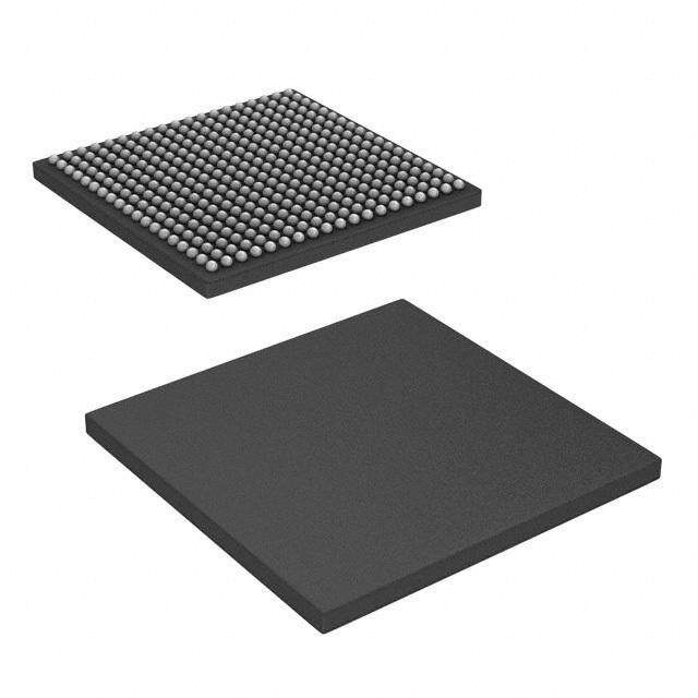
| 描述 | IC USB TRANSCEIVER 14-TSSOPUSB 接口集成电路 USB Transceiver - Lead Free |
| 产品分类 | |
| 品牌 | Micrel |
| 产品手册 | |
| 产品图片 |
|
| rohs | 符合RoHS无铅 / 符合限制有害物质指令(RoHS)规范要求 |
| 产品系列 | 接口 IC,USB 接口集成电路,Micrel MIC2551AYTS- |
| 数据手册 | |
| 产品型号 | MIC2551AYTS |
| 产品目录页面 | |
| 产品种类 | USB 接口集成电路 |
| 供应商器件封装 | 14-TSSOP |
| 其它名称 | 576-2182 |
| 包装 | 管件 |
| 协议 | USB 2.0 |
| 双工 | 半 |
| 商标 | Micrel |
| 安装类型 | 表面贴装 |
| 安装风格 | SMD/SMT |
| 封装 | Tube |
| 封装/外壳 | 14-TSSOP(0.173",4.40mm 宽) |
| 封装/箱体 | TSSOP-14 |
| 工作温度 | -40°C ~ 85°C |
| 工作电源电压 | 4 V to 5.25 V |
| 工作电源电流 | 3.6 mA |
| 工厂包装数量 | 94 |
| 接口类型 | Serial |
| 接收器滞后 | 200mV |
| 数据速率 | 12 Mbps |
| 最大工作温度 | + 85 C |
| 最小工作温度 | - 40 C |
| 标准 | USB 2.0 |
| 标准包装 | 94 |
| 电压-电源 | 4 V ~ 5.25 V |
| 类型 | Transceiver |
| 系列 | MIC2551 |
| 速度 | High-Speed |
| 驱动器/接收器数 | 1/1 |


- 商务部:美国ITC正式对集成电路等产品启动337调查
- 曝三星4nm工艺存在良率问题 高通将骁龙8 Gen1或转产台积电
- 太阳诱电将投资9.5亿元在常州建新厂生产MLCC 预计2023年完工
- 英特尔发布欧洲新工厂建设计划 深化IDM 2.0 战略
- 台积电先进制程称霸业界 有大客户加持明年业绩稳了
- 达到5530亿美元!SIA预计今年全球半导体销售额将创下新高
- 英特尔拟将自动驾驶子公司Mobileye上市 估值或超500亿美元
- 三星加码芯片和SET,合并消费电子和移动部门,撤换高东真等 CEO
- 三星电子宣布重大人事变动 还合并消费电子和移动部门
- 海关总署:前11个月进口集成电路产品价值2.52万亿元 增长14.8%


PDF Datasheet 数据手册内容提取
MIC2551A Micrel, Inc. MIC2551A USB Transceiver General Description Features The MIC2551A is a single chip transceiver that complies with • Compliant to USB Specification Revision 2.0 for full the physical layer specifications of the Universal Serial Bus speed (12Mbs) and low speed (1.5Mbps) operation (USB) 2.0. It supports both full speed (12Mbps) and low • Compliant to IEC-61000-4.2 (Level 3) speed (1.5Mbps) operation and introduces superior edge • Separate I/O supply with operation down to 1.6V rate control, producing crisper eye diagrams, which ease the • Integrated speed select termination supply task of passing USB compliance testing. • Very-low power consumption to meet USB suspend- A unique, patented, dual supply voltage operation allows the current requirements MIC2551A to reference the system I/F I/O signals to a supply • Small TSSOP and MLF® packages voltage down to 1.6V while independently powered by the • No power supply sequencing requirements USB V . This allows the system interface to operate at its • Software controlled re-enumeration BUS core voltage without addition of buffering logic and also Applications reduce system operating current. • PDAs • Palmtops • Cell phones Ordering Information Part Number Standard Pb-Free Package MIC2551ABTS MIC2551AYTS 14-Pin TSSOP MIC2551ABML MIC2551AYML 16-Pin MLF® Typical Application System MIC2551A Supply Voltage VCC GPIO VIF VTRM V BUS CON VBUS OE# VPU R RCV S 1.5k USB USB SIE 20Ω/±1% D+ VP D+ Port Controller D– VM D– R GND SPD 20Ω/±S 1% SUS GND 1.0µF (min) 1µF 10µF (max) 41206ESDA SurgX (See “Applications Information” for additional suppliers.) Typical Application Circuit MicroLeadFrame and MLF are registered trademarks of Amkor Technology. SurgX is a registered trademark of Cooper Electronics Technologies. Micrel, Inc. • 2180 Fortune Drive • San Jose, CA 95131 • USA • tel + 1 (408) 944-0800 • fax + 1 (408) 474-1000 • http://www.micrel.com November 2008 1 M9999-112008
MIC2551A Micrel, Inc. Pin Configuration S U U VIF 1 14 VBUS NC VIF VB VP SPD 2 13 VPU 16 15 14 13 RCV 3 12 VTRM SPD 1 12 VTRM RCV 2 11 D+ VP 4 11 D+ VP 3 10 D– VM 5 10 D- VM 4 9 OE# 5 6 7 8 CON 6 9 OE# GND 7 8 SUS N D S C O N U N C G S 14-Pin TSSOP 16-Pin MLF® (ML) Pin Description Pin Number Pin Number Pin Name I/O Pin Function MIC2551ABTS MIC2551ABML 1 15 VIF I System Interface Supply Voltage: Used to provide reference supply voltage for system I/O interface signaling. 2 1 SPD I Edge Rate Control: A logic HIGH operates at edge rates for “full speed” operation. A logic LOW operates edge rates for “low speed” operation. 3 2 RCV* O Receive Data: Output for USB differential data. 4 3 VP* I/O If OE# = 1, VP = Receiver output (+) If OE# = 0, VP = Driver input (+) 5 4 VM* I/O If OE# = 1 VM, = Receiver output (-) If OE# = 0, VM = Driver input (-) 6 5 CON I CONNECT (Input): Controls state of VPU. Refer to VPU pin description for detail. 7 6 GND Ground Reference. 8 7 SUS I Suspend: Active-High. Turns off internal circuits to reduce supply current. 9 9 OE#* I Output Enable: Active-Low. Enables the transceiver to transmit data onto the bus. When inactive, the transceiver is in the receive mode. 10/11 10/11 D–, D+* I/O Differential data lines conforming to the USB standard. 12 12 VTRM O 3.3V Reference Supply Output: Requires a minimum 0.1µF decoupling capacitor for stability. A 1µF capacitor is recom- mended 13 13 VPU O Pull-up Supply Voltage Output: Used to connect 1.5kΩ pull-up speed detect resistor. If CON = 1, VPU is high impedance. If CON = 0, VPU = 3.3V. 14 14 VBUS I USB Bus Supply Voltage: Used to power USB transceiver and internal circuitry. 8,16 NC No connect. * See Table 1 for description of logic states. M9999-112008 2 November 2008
MIC2551A Micrel, Inc. SUS OE# D+, D– RCV VP/VM Function 0 0 Driving Active Active Normal transmit mode. 0 1 Receiving Active Active Normal receive mode. 1 0 Hi-Z 0 Not active Low power state. 1 1 Hi-Z 0 Active Receiving during suspend (low power state) (Note 1). Note 1. During suspend VP and VM are active in order to detect out-of-band signaling conditions. Table 1. Function Selection OE# = 0: Input Output Result VP VM D+ D- RCV 0 0 0 0 X SE0 0 1 0 1 0 Logic 0 1 0 1 0 1 Logic 1 1 1 1 1 X Undefined OE# = 1: Input Output Result D+ D- VP VM RCV 0 0 0 0 X SE0 0 1 0 1 0 Logic 0 1 0 1 0 1 Logic 1 1 1 1 1 X Undefined X - Undefined Table 2. Truth Table During Normal Mode November 2008 3 M9999-112008
MIC2551A Micrel, Inc. Absolute Maximum Ratings (Note 1) Operating Ratings (Note 2) Supply Voltage (V ) .................................................6.5V Supply Voltage (V ) ................................. 4.0V to 5.25V BUS BUS All Other Inputs ............................................. –0.5V to 5.5V Ambient Operating Temperature................–40°C to +85°C Ambient Storage Temperature.................–65°C to +150°C Package Thermal Resistance Output Current (D+, D–)..........................................± 50mA TSSOP (θJA) ..................................................100(°C/W) MLF® (θ ) ....................................................... 59(°C/W) Output Current (all others) .......................................±15mA JA Input Current............................................................±50mA ESD, Note 3 V , D+, D–........................................................±11KV BUS All other pins ..........................................................±2KV DC Electrical Characteristics (System and USB Interface) (Note 7) V = 3.6V, V = 5V unless otherwise noted; T = 25°C. Bold indicates specifications over temperature, –40°C to 85°C. IF BUS A Symbol Parameter Conditions Min Typ Max Units V USB Supply Voltage 4.0 5.25 V BUS V System I/F Supply Voltage 1.6 3.6 V IF V LOW-Level Input Voltage, Note 4 V –0.3 0.15V V IL IF IF V HIGH-Level Input Voltage, Note 4 0.85V V +0.3 V IH IF IF V HIGH-Level Output Voltage, Note 4 I = 20µA 0.9V V OH OH IF V LOW-Level Output Voltage, Note 4 I = 20µA 0.1 V OL OL I Input Leakage Current, Note 4 –5 5 µA IL Symbol Parameter Conditions Min Typ Max Units SPD SUS OE# Voltage Load 1 0 1 1 5 µA 1 0 0 1 5 µA 0 0 1 1 5 µA I VIF Supply Current 0 0 0 VBUS = 5.25V 1 5 µA IF 0 1 0 VIF = 3.6V 1 5 µA 1 0 0 f = 6MHz CLOAD 325 650 µA = 50 pF, Note 7 f = 750kHz 0 0 0 CLOAD = 600 pF 40 75 µA Note 7 1 0 1 800 1100 µA 1 0 0 3000 5000 µA 0 0 1 230 350 µA 0 0 0 400 700 µA I VBUS Supply Current 0 1 0 VBUS = 5.25V 130 200 µA VBUS 1 0 0 VIF = 3.6V f = 6MHz CLOAD 7.3 10 mA = 50 pF, Note 7 f = 750kHz 0 0 0 CLOAD = 600 pF 3.6 5 mA Note 7 I VPU Leakage Current CON = 1, V = 0V –5 5 µA VPULEAK PU I VIF Leakage Current V = 3.6V, V = 0V –5 5 µA VIFLEAK IF BUS V Pull-Up Output Voltage I = 200µA, V = 4.0 to 5.25V 3.0 3.3 3.6 V PU TERM BUS R Internal Pull-Up Termination I = 10mA, V = 4.0 to 5.25V 10 Ω SW TERM BUS ESD Protection IEC-1000-4-2 Air Discharge 10 pulses ±8 kV (D+, D–, Contact Discharge 10 pulses ±9 kV V only) BUS M9999-112008 4 November 2008
MIC2551A Micrel, Inc. DC Electrical Characteristics (Transceiver) (Note 7) Symbol Parameter Conditions Min Typ Max Units Leakage Current I Hi-Z State Data Line Leakage 0V < V < 3.3V, SUS = 1 –10 10 µA LO IN (Suspend Mode) Input Levels V Differential Input Sensitivity |(D+) – (D–)| 0.2 V DI V Differential Common Mode Range Includes V range 0.8 2.5 V CM DI V Single-Ended Receiver Threshold 0.8 2.0 V SE Receiver Hysteresis 200 mV Output Levels V Static Output Low R = 1.5kΩ to 3.6V 0.3 V OL L V Static Output High R = 15kΩ to GND 2.8 3.6 V OH L Capacitance C Transceiver Capacitance Pin to GND 10 pF IN Z Driver Output Resistance Steady state drive 8 16 24 Ω DRV AC Electrical Characteristics (Notes 6, 7) Driver Characteristics (Low Speed) T Transition Rise Time C = 50pF, Figure 2 75 ns R L C = 600pF 300 L T Transition Fall Time C = 50pF, Figure 2 75 ns F L C = 600pF 300 L T , T Rise/Fall Time Matching (T , T ) 80 125 % R F R F V Output Signal Crossover Voltage 1.3 2.0 V CRS Driver Characteristics (Full Speed) T Transition Rise Time C = 50pF, Figure 2 4 20 ns R L T Transition Fall Time C = 50pF, Figure 2 4 20 ns F L T , T Rise/Fall Time Matching (T , T ) 90 111.11 % R F R F V Output Signal Crossover Voltage 1.3 2.0 V CRS Transceiver Timing t OE# to RCVR Tri-State Delay Figure 1 15 ns PVZ t Receiver Tri-State to Transmit Delay Figure 1 15 ns PZD t OE# to DRVR Tri-State Delay Figure 1 15 ns PDZ t Driver Tri-State to Receive Delay Figure 1 15 ns PZV t VP, VM to D+, D– Propagation Delay Figure 4 15 ns PLH t PHL t D+, D– to RCV Propagation Delay Figure 3 15 ns PLH t PHL t D+, D– to V , V Propagation Delay Figure 3 8 ns PLH P M t PHL Note 1. Exceeding the absolute maximum rating may damage the device. Note 2. The device is not guaranteed to function outside its operating rating. Note 3. Devices are ESD sensitive. Handling precautions recommended. Human body model, 1.5k in series with 100pF. Note 4. Specification applies to the following pins: SUS, SPD, RCV, CON, RCV, VP, VM, OE#. Note 5. Characterized specification(s), but not production tested. Note 6. All AC parameters guaranteed by design but not production tested. Note 7. Specification for packaged product only. November 2008 5 M9999-112008
MIC2551A Micrel, Inc. Timing Diagrams TRANSMIT RECEIVE OE# t t PVZ PZV V /V P M t t PZD PDZ D+/D– Figure 1. Enable and Disable Times Rise Time Fall Time Differential 90% 90% Data Lines 10% 10% t t R F Figure 2. Rise and Fall Times D+ Differential V V CRS Data Lines CRS D– V tPLH tPHL OH V OL V SS Figure 3. Receiver Propagation Delay V OH V OL t t PLH PHL D+ Differential V V CRS Data Lines CRS D– Figure 4. Driver Propagation Delay Test Circuits D.U.T. 25pF Figure 5. Load for V , V , RCV P M VTRM 15k 20Ω D.U.T. 15k C L Figure 6. Load for D+, D– M9999-112008 6 November 2008
MIC2551A Micrel, Inc. Functional Diagram To Internal Circuitry LDO VBUS Regulator VIF VTERM VPU CON D+ SPD OE# D– RCV or elat Levansl Tr VP VM SUS GND MIC2551A Applications Information The MIC2551A is designed to provide USB connectivity in In addition, a 3.3V, 10% termination supply voltage, (V ), is PU mobile systems where available system supply voltages are provided to support speed selection. V can be disabled or PU not able to satisfy USB requirements. The MIC2551A can enabled under software control via the CON input. This operate down to supply voltages of 1.6V and still meet USB allows for software-controlled connect or disconnect states. physical layer specifications. As shown in the circuit above, A 1.5k resistor is required to be connected between this pin the MIC2551A takes advantage of the USB supply voltage, and the D+ or D– lines to respectively specify high speed or V , to operate the transceiver. The system voltage, V , is low speed operation. BUS IF used to set the reference voltage used by the digital I/O lines The use of ESD transient protection devices is not required interfacing to the system controller. Internal circuitry provides for operation, but is recommended. The MIC2551A is ESD translation between the USB and system voltage domains. rated for 11kV at the VBUS and D+, D– pins and 2kV for all V will typically be the main supply voltage rail for the IF other pins. controller. November 2008 7 M9999-112008
MIC2551A Micrel, Inc. Power Supply Configuration Suspend The MIC2551A can be set up for different power supply When the suspend pin (SUS) is high, power consumption is configurations which modify the behavior of the device. Both reduced to a minimum. V is not disabled. RCV, V and V TRM P M V and V have special thresholds that detect when they are still functional to enable the device to detect USB activity. BUS IF are either removed or grounded. Table 3 depicts the behavior For minimal current consumption in suspend mode, it is under the different power supply configuration scenarios that recommended that OE# = 1, and SPD = 0. are explained below. Speed Normal Mode The speed pin (SPD) sets D+/D– output edge rates by increas- V is connected to the 5.0V USB bus voltage and V is ing or decreasing biasing current sources within the output BUS IF connected to a supply voltage in the range of 1.6V to 3.6V. In drivers. For low speed, SPD = 0. For full speed, SPD = 1. By this case V supplies a 3.3V voltage for powering the setting SPD = 0 during idle periods, in conjunction with suspend TRM speed select resistor via V depending on the state of CON (SUS), the lowest quiescent current can be obtained. However, PU pin. designers must provide a 300ns delay between changing SPD Disconnect Mode from 0 to 1 and transmission of data at full speed. This delay V is connected to a supply in a range of 1.6V to 3.6V and ensures the output drivers have arrived at their proper operating IF V is open or grounded. If V is opened while transmit- conditions. Failure to do so can result in leading edge distortion BUS BUS ting, the data lines (D+, D–) have sharing capability and may on the first few data bits transmitted. be driven with external devices up to approximately 3.6V if External ESD Protection and only if SUSPEND is enabled (SUS = 1). With V BUS The use of ESD transient protection devices is not required ground, D+, D– sharing mode is not permitted. for operation, but is recommended. We recommend the Disable Mode following devices or the equivalent: VBUS is connected to the 5.0V USB bus voltage and VIF is Cooper Electronic Technologies (www.cooperet.com) open. All logic controlled inputs become high impedances, 41206ESDA SurgX thus minimal current will be supplied by V if the input pins are IF 0805ESDA SurgX pulled up to an external source. Alternate Power Supply Configuration Options Littelfuse (www.littelfuse.com) I/O Interface Using 3.3V V0402MHS05 In systems where the I/O interface utilizes a 3.3V USB SP0503BAHT controller, an alternate solution is shown in Figure 7. No extra Non-Multiplexed Bus components are required; however, the load on V must TRM In order to save pin count for the USB logic controller not exceed 10mA. interface, the MIC2551A was designed with V and V as bi- P M 3.3V directional pins. To interface the MIC2551A with a non- multiplexed data bus, resistors can be used for low cost MIC2551 VDD VIF VBUS VBUS isolation as shown in Figure 8. USB USB Logic Controller Controller I/O V /V / VTRM (SIE) MIC2551 P M RCV/OE# V V P P 10k Figure 7. I/O Interface Using 3.3V V PO V V Signal Amplitude Respective to VIF M 10k M When operating the MIC2551A, it is necessary to provide V MO input signals which do not exceed V + 0.3V. IF Figure 8. MIC2551A Interface to Non-Multiplexed Data Bus Configuration Mode VBUS/VTRM VIF Notes Normal Connected Connected Normal supply configuration and operation. Disconnect Open Connected VP/VM are HIGH outputs, RCV is LOW. (D+/D– sharing) With OE# = 0 and SUS = 1, data lines may be driven with external devices up to 3.6V. With D+, D– floating, I draws less than 1µA. IF Disconnect Ground Connected VP/VM are HIGH outputs, RCV is LOW. With D+, D– floating, I draws less than 1µA. IF Disable Mode Connected Open Logic controlled inputs pins are Hi-Z. Prohibited Connected Ground Prohibited condition. Table 3. Power Supply Configuration M9999-112008 8 November 2008
MIC2551A Micrel, Inc. PCB Layout Recommendations Although the USB standard and applications are not based in an impedance controlled environment, a properly designed PCB layout is recommended for optimal transceiver perfor- mance. The suggested PCB layout hints are as follows: • Match signal line traces (VP/VM, D+, D–) to 40ps, approximately 1/ inch if possible. FR-4 3 PCB material propagation is about 150ps/inch, so to minimize skew try to keep VP/VM, D+/D– traces as short as possible. • For every signal line trace width (w), separate the signal lines by 1.5 – 2 widths. Place all other traces at >2 widths from all signal line traces. • Maintain the same number of vias on each differential trace, keeping traces approximately at same separation distance along the line. • Control signal line impedances to ±10%. • Keep R as close to the IC as possible, with S equal distance between R and the IC for both S D+ and D–. November 2008 9 M9999-112008
MIC2551A Micrel, Inc. Package Information 4.50 (0.177)(cid:0) 6.4 BSC (0.252)(cid:0) DIMENSIONS:(cid:0) 4.30 (0.169) (cid:0) MM (INCH) 0.30 (0.012)(cid:0) 0.19 (0.007) 5.10 (0.200)(cid:0) 4.90 (0.193) 0.20 (0.008)(cid:0) 1.10 MAX (0.043) 0.09 (0.003) 0.65 BSC(cid:0) 1.00 (0.039) REF (0.026)(cid:0) 8°(cid:0) (cid:0) 0.15 (0.006)(cid:0) 0°(cid:0) 0.70 (0.028)(cid:0) 0.05 (0.002) 0.50 (0.020) 14-lead TSSOP (TS) 0.42+0.18 –0.18 0.85+–00..6155 0.23+–00..0057 3.00BSC 0.65+0.15 0.01+–00..0014 1.60+–00..1100 2.75BSC –0.65 0.20 REF. 0.42+–00..1188 PIN 1 ID 16 N 1 1 0.50 DIA 23 2.75BSC 3.00BSC 23 1.60+–00..1100 4 4 12° max 0.42+0.18 0.5 BSC 0.40+–00..0055 –0.18 SEATING(cid:0) 1.5 REF PLANE TOP VIEW BOTTOM VIEW CC 1. DIMENSIONS ARE IN mm.(cid:0) 0.23+0.07 CL 4 –0.05 2. DIE THICKNESS ALLOWABLE IS 0.305mm MAX.(cid:0) 0.01+0.04 3. PACKAGE WARPAGE MAX 0.05mm.(cid:0) –0.01 4. THIS DIMENSION APPLIES TO PLATED TERMINAL AND IS MEASURED SECTION "C-C" BETWEEN 0.20mm AND 0.25mm FROM TIP.(cid:0) 0.5BSC SCALE: NONE 5. APPLIES ONLY FOR TERMINALS FOR EVEN TERMINAL/SIDE Rev. 02 16-Pin MLF® (ML) M9999-112008 10 November 2008
MIC2551A Micrel, Inc. 16-Pin MLF® (ML) MICREL INC. 2180 FORTUNE DRIVE SAN JOSE, CA 95131 USA TEL + 1 (408) 944-0800 FAX + 1 (408) 474-1000 WEB http://www.micrel.com This information furnished by Micrel in this data sheet is believed to be accurate and reliable. However no responsibility is assumed by Micrel for its use. Micrel reserves the right to change circuitry and specifications at any time without notification to the customer. Micrel Products are not designed or authorized for use as components in life support appliances, devices or systems where malfunction of a product can reasonably be expected to result in personal injury. Life support devices or systems are devices or systems that (a) are intended for surgical implant into the body or (b) support or sustain life, and whose failure to perform can be reasonably expected to result in a significant injury to the user. A Purchaser’s use or sale of Micrel Products for use in life support appliances, devices or systems is a Purchaser’s own risk and Purchaser agrees to fully indemnify Micrel for any damages resulting from such use or sale. © 2004 Micrel, Incorporated. November 2008 11 M9999-112008
Mouser Electronics Authorized Distributor Click to View Pricing, Inventory, Delivery & Lifecycle Information: M icrochip: MIC2551AYML TR MIC2551AYML25 TR MIC2551AYTS MIC2551AYML-TR MIC2551AYTS-TR MIC2551AYML25- TR