- 型号: MIC2012PZM
- 制造商: Micrel
- 库位|库存: xxxx|xxxx
- 要求:
| 数量阶梯 | 香港交货 | 国内含税 |
| +xxxx | $xxxx | ¥xxxx |
查看当月历史价格
查看今年历史价格
MIC2012PZM产品简介:
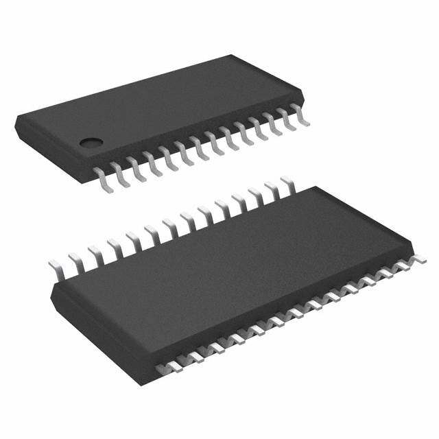
ICGOO电子元器件商城为您提供MIC2012PZM由Micrel设计生产,在icgoo商城现货销售,并且可以通过原厂、代理商等渠道进行代购。 MIC2012PZM价格参考¥询价-¥询价。MicrelMIC2012PZM封装/规格:接口 - 控制器, USB 控制器 8-SOIC。您可以下载MIC2012PZM参考资料、Datasheet数据手册功能说明书,资料中有MIC2012PZM 详细功能的应用电路图电压和使用方法及教程。
| 参数 | 数值 |
| 产品目录 | 集成电路 (IC)半导体 |
| 描述 | IC USB PWR CTRLR DUAL 8-SOICUSB开关IC USB Power Controller - Lead Free |
| 产品分类 | |
| 品牌 | Micrel Inc |
| 产品手册 | |
| 产品图片 |
|
| rohs | 符合RoHS无铅 / 符合限制有害物质指令(RoHS)规范要求 |
| 产品系列 | 开关 IC,USB开关IC,Micrel MIC2012PZM- |
| 数据手册 | |
| 产品型号 | MIC2012PZM |
| 产品目录页面 | |
| 产品种类 | USB开关IC |
| 供应商器件封装 | 8-SOIC |
| 其它名称 | 576-2136 |
| 功能 | 控制器 |
| 包装 | 管件 |
| 协议 | USB |
| 商标 | Micrel |
| 安装风格 | SMD/SMT |
| 导通电阻—最大值 | 140 mOhms |
| 封装 | Tube |
| 封装/外壳 | 8-SOIC(0.154",3.90mm 宽) |
| 封装/箱体 | SOIC-8 |
| 工作温度 | 0°C ~ 70°C |
| 工厂包装数量 | 95 |
| 开关数量 | Dual |
| 开关电流—典型值 | 500 mA |
| 开关配置 | N-Channel |
| 接口 | - |
| 最大工作温度 | + 70 C |
| 最小工作温度 | 0 C |
| 标准 | - |
| 标准包装 | 95 |
| 电压-电源 | 4.5 V ~ 5.5 V |
| 电流-电源 | 16µA |
| 电源电压-最大 | 5.5 V |
| 电源电压-最小 | 4.5 V |
| 电源电流 | 16 uA |
| 空闲时间—最大值 | 35 us |
| 系列 | MIC2012 |
| 运行时间—最大值 | 2 ms |





- 商务部:美国ITC正式对集成电路等产品启动337调查
- 曝三星4nm工艺存在良率问题 高通将骁龙8 Gen1或转产台积电
- 太阳诱电将投资9.5亿元在常州建新厂生产MLCC 预计2023年完工
- 英特尔发布欧洲新工厂建设计划 深化IDM 2.0 战略
- 台积电先进制程称霸业界 有大客户加持明年业绩稳了
- 达到5530亿美元!SIA预计今年全球半导体销售额将创下新高
- 英特尔拟将自动驾驶子公司Mobileye上市 估值或超500亿美元
- 三星加码芯片和SET,合并消费电子和移动部门,撤换高东真等 CEO
- 三星电子宣布重大人事变动 还合并消费电子和移动部门
- 海关总署:前11个月进口集成电路产品价值2.52万亿元 增长14.8%



PDF Datasheet 数据手册内容提取
MIC2012 Micrel MIC2012/MIC2072 USB Power Controller General Description Features The MIC2012 is a dual channel USB power switch designed to • Compliant to USB power distribution specifi cations support the power distribution requirements for USB Wakeup • UL Recognized Component from the ACPI S3 state. The MIC2012 will directly switch its • Two completely independent switches two outputs between a 5V main supply and a 5V auxiliary • Integrated switching matrix supports ACPI S0/S3 state supply normally provided in ATX style power supplies. transitions without external FET circuits The MIC2012 will adjust its current-limit threshold according • Make-before-break switching ensures glitch-free to the ACPI state it is in. In the normal active S0 state the cur- transitions rent-limit is set at 500mA minimum per channel satisfying the • No back-feed of auxiliary supply onto main supply dur- USB continuous output current specifi cation. In the S3 state ing standby mode the current-limit can be reduced to only 100mA per channel • Bi-level current-limit preserves auxiliary supply voltage to minimize the current that is supplied by the auxiliary supply regulation in standby mode thereby ensuring that voltage regulation is maintained even • Thermally isolated channels during fault conditions. • Thermal shutdown protection • Fault status outputs with fi lter prevents false assertions The MIC2012 provides make-before-break switching to ensure during hot-plug events glitch-free transitions between the S3 and S0 states. Each • Latched thermal shutdown options with auto-reset channel is also thermally isolated from the other so that a (MIC2072) fault in one channel does not effect the other. FAULT status • Undervoltage lockout output signals are also provided indicating overcurrent and thermal shutdown conditions. Applications The MIC2072 option latches the output off upon detecting an overcurrent condition for more than 5ms minimum. The • Desktop PCs output can be reset by either toggling the EN inputs of the • Notebook PCs MIC2072-1, -2 or by removing the load. Latching the output • Notebook Docking stations off provides a circuit breaker mode of operation which reduces • LAN Servers power consumption during fault conditions. • PC Motherboards Typical Application ATX Power Supply 5V MAIN V 5V STANDBY BUS Downstream D+ MIC2012P USB D– Port 1 MAIN OUT1 GND AUX OUT2 100F S3 Control S3# FAULT1# VBUS Downstream FAULT2# D+ USB GND D– Port 2 100F 82801AA or Equivalent GND SLP S3# SLP S5# Overcurrent Port 1 OC0 Overcurrent Port 1 OC1 Figure 1. USB Wakeup with Control Input UL Recognized Component Micrel, Inc. • 2180 Fortune Drive • San Jose, CA 95131 • USA • tel + 1 (408) 944-0800 • fax + 1 (408) 474-1000 • http://www.micrel.com January 2005 1 MIC2012/2072
MIC2012 Micrel Ordering Information Part Number Circuit Breaker Temperature Standard Pb-Free Enable Fault Output Range Range Package MIC2012BM(1) MIC2012YM(1) n/a Open-Drain 0°C to +70°C 8-lead SOIC MIC2012CM MIC2012ZM n/a Open-Drain 0°C to +70°C 8-lead SOIC MIC2012PCM MIC2012PZM n/a Internal Pull-Up 0°C to +70°C 8-lead SOIC MIC2012-1PCQS MIC2012-1PZQS Active High Internal Pull-Up 0°C to +70°C 16-lead QSOP MIC2012-2PCQS MIC2012-2PZQS Active Low Internal Pull-Up 0°C to +70°C 16-lead QSOP MIC2072-1PCQS MIC2072-2PZQS Active High Internal Pull-Up Δ 0°C to +70°C 16-lead QSOP MIC2072-2PCQS MIC2072-2PZQS Active Low Internal Pull-Up Δ 0°C to +70°C 16-lead QSOP Note: 1. Contact factory for availablity Pin Confi guration FAULT1 1 16 FAULT2 EN1 2 15 EN2 FAULT1 1 8 FAULT2 S3# 3 14 OUT1 S3# 2 7 OUT1 NC 4 13 OUT1 AUX 3 6 MAIN AUX 5 12 MAIN GND 4 5 OUT2 NC 6 11 MAIN 8-Pin SOIC (M) NC 7 10 OUT2 GND 8 9 OUT2 16-Pin QSOP (QS) MIC2012/2072 2 January 2005
MIC2012 Micrel Pin Description Pin Number Pin Number Pin Name Pin Function (MIC2012) (MIC2012-1, -2) 1 1 FAULT1 Fault Status (Output): Internal pull-up or open-drain. Asserted LOW when Channel is in a thermal shutdown state or overcurrent condition for more than 5ms. MIC2072 latches this output in its asserted state upon an over- current condition. Toggling EN1 or removing the load will reset the circuit breaker latch and deassert FAULT1. n/a 2 EN1 Enable (Input): Channel 1, active-high (–1) or active-low (–2). Toggling this input also resets the latched output of the MIC2072. 2 3 S3# Control (Input): When this input is HIGH, the MAIN inputs are connected to OUT1 and OUT2 via 100mΩ MOSFET switches. When this input is LOW the AUX inputs are connected to OUT1 and OUT2 via 500mΩ MOSFET switches. 3 5 AUX Auxiliary 5V Supply (Input): Also used as power supply for internal circuitry. n/a 4, 6, 7 NC No Connection: This pin may be connected to other pins without restriction. 4 8 GND Ground 5 9, 10 OUT2 Channel 2 (Output): For MIC2012-1, -2 both pins must be externally con- nected together. 6 11, 12 MAIN 5V Main Supply (Input): All MAIN inputs must be connected together exter- nally. 7 13, 14 OUT1 Channel 1 (Output): For MIC2012-1, -2 both pins must be externally con- nected together. n/a 15 EN2 Enable (Input): Channel 2, active-high (–1) or active-low (–2). Toggling this input also resets the latched output of the MIC2072. 8 16 FAULT2 Fault Status (Output): Internal pull-up or open-drain. Asserted LOW when Channel 2 is in a thermal shutdown state or overcurrent condition for more than 5ms. MIC2072 latches this output in its asserted state upon an over- current condition. Toggling EN2 or removing the load will reset the circuit breaker latch and deassert FAULT2. January 2005 3 MIC2012/2072
MIC2012 Micrel Absolute Maximum Ratings (Note 1, Note 4) Operating Ratings (Note 2) Supply Voltage (V V V ) .....................–0.3V to 6V Supply Voltage (V V ) ......................+4.5V to +5.5V IN, MAIN, AUX MAIN, AUX EN1, EN2, S3# Input Pins .................................–0.3V to 6V Ambient Temperature (T ) ............................–0°C to +70°C A FAULT#, OUT1, OUT2 Output Pins ...................–0.3V to 6V Junction Temperature (T ) ........................Internally Limited J FAULT Output Current ................................................25mA Package Thermal Resistance ESD Rating, Note 3 ......................................................2kV QSOP (θJA) .......................................................................163°C/W SOIC (θ ) .........................................................................160°C/W JA Electrical Characteristics V = 5V; AUX = 5V; T = 25°C; unless noted MAIN A Symbol Parameter Condition Min Typ Max Units V MAIN Supply Voltage 4.5 5.0 5.5 V MAIN I MAIN Supply Current Switches On S3# = 1, no load 16 22 µA MAIN (ON) Note 5 I MAIN Supply Current Switches Off S3# = 1, no load 5 µA MAIN (OFF) Note 5, (MIC20x2-1, MIC20x2-2 only) I MAIN Reverse Leakage Current, S3# = 0, both switches ON, V = 0V –10 +10 µA LEAK MAIN V AUX Supply Voltage 4.5 5.0 5.5 V AUX I AUX Supply Current, No load 0.6 1 mA AUX ON both switches on, Note 5 S3# = 0 I AUX Supply Current, switches No load 5 µA AUX OFF off. (MIC20x2-1, MIC20x2-2 only) S3# = 0 V AUX Undervoltage Lockout V increasing 3.1 4.0 V UV/AUX AUX Threshold V decreasing 2.9 3.8 V AUX V AUX Undervoltage Lockout 200 mV HYS Hysteresis R MAIN On-Resistance, Each Output S3# = 1, I = 500mA 100 140 mΩ DSMAIN OUT R AUX On-Resistance, Each Output S3# = 0, I = 100mA 500 700 mΩ DSAUX OUT I MAIN Current-Limit Threshold S3# = 1, V = 4.0V, ramped load 0.8 2.0 A LIMIT(MAIN) OUT MAIN Short-Circuit Current-Limit V = 0V 0.65 1.8 A OUT I AUXCurrent-Limit Threshold S3# = 0, V = 4.0V, ramped load 105 150 195 mA LIMIT(AUX) OUT AUX Short-Circuit Current-Limit V = 0V, C = 100µF 80 mA OUT OUT V S3#, EN1, EN2. Input High-to-Low transition 0.8 1.5 V TH Threshold Voltage Low-to-High transition 1.7 2.0 V (EN1, EN2, for MIC20x2-x only) V EN1, EN2 and S3# Input Hysteresis 200 mV HYS (EN1, EN2, for MIC20x2-x only) I S3#, EN1, EN2 Input Current V = 5V, 0V –1 1 µA IN S3/EN (EN1, EN2, for MIC20x2-x only) I OUT1, OUT2 Leakage Current Outputs are off, V = 0 –10 10 µA OFF OUT (MIC2012-x, MIC2072-x only) Pull-Up Current During Latched Outputs latched off 1 mA Output State (MIC2072-1, -2) MIC2012/2072 4 January 2005
MIC2012 Micrel Symbol Parameter Condition Min Typ Max Units V Latch Reset Threshold V Rising 1.95 V TH LATCH OUT (MIC2072, MIC2072-x only) Minimum Output Slew Rate 0.4 V/s to Reset Latch (MIC2072, MIC2072-x only), Note 6 Overtemperature Threshold T increasing, single channel 140 °C J T decreasing, single channel 120 °C J T increasing, both channels 160 °C J T decreasing, both channels 150 °C J V FAULT Output Low Voltage I = 5mA 0.2 V OL FAULT V FAULT Output High Voltage I = –20µA 4 V OH FAULT (MIC2012-1P,-2P),(MIC2072-1P,-2P) FAULT Output Off Current V = 5V 0.2 10 µA FAULT (Not Applicable to 'P' Options) T MAIN to S3# Hold Time, Note 6 Figure 5 5 ms H T MAIN to S3# Set-up Time, Note 6 Figure 5 0 ms S t FAULT Delay Filter Response Time Output shorted to ground, Figure 4 5 10 20 ms DLY (Overcurrent only), Note 7 t Overcurrent Response Time Output shorted to ground, Figure 4 OC MAIN output 2 µs AUX output 2 µs t MAIN Output Turn-On Time R = 10Ω, C = 1µF, Figure 3 2 ms ON(MAIN) L L t MAIN Output Turn-Off Time R = 10Ω, C = 1µF, Figure 3 35 µs OFF(MAIN) L L (MIC20x2-x only) t MAIN Output Rise Time R = 10Ω, C = 1µF, Figure 3 2 ms r(MAIN) L L t MAIN Output Fall Time R = 10Ω, C = 1µF, Figure 3 32 µs f(MAIN) L L (MIC20x2-x only) t AUX Output Turn-On Time R = 50Ω, C = 1µF, Figure 3 0.6 ms ON(AUX) L L t AUX Output Turn-Off Time R = 50Ω, C = 1µF, Figure 3 120 µs OFF(AUX) L L (MIC20x2-x only) t AUX Output Rise Time R = 50Ω, C = 1µF, Figure 3 0.5 ms r(AUX) L L t AUX Output Fall Time R = 50Ω, C = 1µF, Figure 3 115 µs f(AUX) L L (MIC20x2-x only) t MAIN to AUX S3# transition to 0 5 7.5 ms XMA Cross Conduction Time, Note 8 t AUX to MAIN S3# transition to 1 5 7.5 ms XAM Cross Conduction Time, Note 8 Note 1. Exceeding the absolute maximum rating may damage the device. Note 2. The device is not guaranteed to function outside its operating rating. Note 3. Devices are ESD sensitive. Handling precautions recommended. Human body model, 1.5k in series with 100pF. Note 4. All voltages are referenced to ground. Note 5. For MIC20x2-1(P) OFF occurs when V < 0.8V and ON occurs when V > 2.4V. For MIC20x2-2(P) OFF occurs when V > 2.4V and ON EN EN EN occurs when V < 0.8V. EN Note 6. Guaranteed by design. Not production tested. Note 7. Assumes only one channel in current-limit. Delay circuitry is shared among channels so it is possible for t to be 40ms max if one channel DLY enters current-limit as the other is about to time-out. Note 8. Cross conduction time is the duration in which both MAIN and AUX internal switches are on subsequent to S3# transitioning. January 2005 5 MIC2012/2072
MIC2012 Micrel Timing Diagrams 50% VEN tOFF tON 90% VOUT 10% Figure 2. MIC2012/72-1 50% VEN tOFF tON 90% VOUT 10% Figure 3. MIC2012/72-2 Output shorted to ground V OUT I I OUT LIMIT t FAULT# OC t DLY Figure 4. Overcurrent Response Timing tH tS MAIN S3# 1.5V 1.5V Figure 5. MAIN to S3# Timing MIC2012/2072 6 January 2005
MIC2012 Micrel Test Circuit V OUT Device IOUT Under OUT Test R C L L tr tf 90% 90% V OUT 10% 10% January 2005 7 MIC2012/2072
MIC2012 Micrel Typical Characteristics Main Supply Current Main Supply Current vs. Temperature vs. Temperature Main Short-Circuit Current-Limit (Main 1 and Main 2 = ON) (Main 1 and Main 2 = OFF) vs. Temperature 30 0.25 1.30 25 VENM1AI N= E=N 42.5, 5=. 0[O, 5N.5],VVAUX = S3# = 5.0V 0.202.52 VENM1AI N= E=N 42.5, 5=.0 [O, 5F.5FV],VAUX = S3# = 5.0V 1.25 VVAMUAXIN = = S 53.#0 V= 4.5, 5.0, 5.5V 20 5.5VMAIN 0.01.7155 5.5VMAIN 5.0VMAIN 1.20 15 0.125 1.15 5.0V 4.5VMAIN MAIN 0.1 5.5VAUX 10 1.10 5.0V 0.075 AUX 4.5V 0.05 MAIN 5 1.05 4.5V I = 0µA 0.025 I = 0µA AUX OUT OUT 0 0 1.00 -40 -20 0 20 40 60 80 100 -40 -20 0 20 40 60 80 100 -40 -20 0 20 40 60 80 100 TEMPERATURE (°C) TEMPERATURE (°C) TEMPERATURE (°C) Main Short-Circuit Main Rise-Time AUX Supply Current Current-Limit Threshold vs. Temperature vs. Temperature vs. Temperature (EN Toggled) (AUX 1 and AUX 2 = ON) 1.40 2000 1000 1.35 VVAMUAXIN = = S 53.#0 V= 4.5, 5.0, 5.5V 11680000 VVAMUAXIN = = S 53.#0 V= 4.5, 5.0, 5.5V 4.5VAUX 890000 VVAMUAXIN = = 4 S.53, #5 .=0 ,0 5V.5V 5.5VAUX 1.30 1400 700 5.5V AUX 1200 5.0V 600 1.25 AUX 1000 500 1.20 5.0V 800 400 4.5VAUX 5.0VAUX AUX 1.15 4.5VAUX 460000 5.5VAUX RCLL == 110µΩF 230000 IEONU1T == E0Nµ2A = [ON] 1.10 200 100 -40 -20 0 20 40 60 80 100 -40 -20 0 20 40 60 80 100 -40 -20 0 20 40 60 80 100 TEMPERATURE (°C) TEMPERATURE (°C) TEMPERATURE (°C) AUX Supply Current Enable Threshold (increasing) Enable Threshold (decreasing) vs. Temperature vs. Temperature vs. Temperature (AUX 1 and AUX 2 = OFF) (MIC2012-1/-2) (MIC2012-1/-2) 1.00 2.2 2.0 00..8900 VVIOAMUUATXIN == = 04 µS.5A3, #5 .=0 ,0 5V.5V 2.0 5.5VAUX 1.8 VVAMUAXIN = = 4 S.53,# 5 =.0 5, 5.0.5VV 0.70 EN1 = EN2 = [OFF] 0.60 1.8 1.6 0.50 5.0VAUX 4.5V 5.5VAUX 0.40 1.6 4.5V 1.4 AUX AUX 00..2300 5.0V 5.5VAUX 4.5VAUX 1.4 VAUX = 4.5, 5.0, 5.5V 1.2 5.0VAUX 0.10 AUX V = S3# = 5.0V MAIN 0.00 1.2 1.0 -40 -20 0 20 40 60 80 100 -40 -20 0 20 40 60 80 100 -40 -20 0 20 40 60 80 100 TEMPERATURE (°C) TEMPERATURE (°C) TEMPERATURE (°C) Enable Threshold (increasing) Enable Threshold (decreasing) Pull-Up Current vs. Temperature vs. Temperature vs. Temperature (MIC2012-1/-2) (MIC2012-1/-2) (Output Latched Off–MIC2072) 2.2 2.0 1800 V = 5.0V MAIN 2.0 1.8 4.5VMAIN 1600 VAUX = S3# = 4.5, 5.0, 5.5V 5.5V 1400 MAIN 1.8 4.5VMAIN 5.0VMAIN 1.6 5.0VMAIN 1200 5.5VAUX 1000 1.6 1.4 5.5V 800 MAIN 5.0V 1.4 VMAIN = 4.5V to 5.5V 1.2 V = 4.5V to 5.5V 600 AUX 4.5VAUX VAUX = S3# = 5.0V VAMUAXIN = S3# = 5.0V 400 1.2 1.0 200 -40 -20 0 20 40 60 80 100 -40 -20 0 20 40 60 80 100 -40 -20 0 20 40 60 80 100 TEMPERATURE (°C) TEMPERATURE (°C) TEMPERATURE (°C) MIC2012/2072 8 January 2005
MIC2012 Micrel Output Reset Threshold vs. Temperature 3.00 (Output Latched Off–MIC2072) V Rising 2.75 OUT VMAIN = 5.0V 2.50 VAUX = S3# = 4.5, 5.0, 5.5V 5.5V AUX 2.25 2.00 1.75 4.5V 5.0VAUX AUX 1.50 -40 -20 0 20 40 60 80 100 TEMPERATURE (°C) January 2005 9 MIC2012/2072
MIC2012 Micrel Functional Characteristics AUX Start-up by UVLO AUX Shutdown by UVLO VFAULTVIAUXOUTOUT(2V/div)(2V/div)(2V/div)(50mA/div) VVERCVNAMLLMOOUA XAAI=AN DD r I =a[N==O m S51N=p30F] s#CV f=rLAo R0Um=VXL 0 1 =V=0 t501o VF05V VFAULTVIAUXOUTOUT(2V/div)(2V/div)(2V/div)(50mA/div) VVERCAMNLLOOUA XAAI=N DD r =a[==O m S51Np30F]s# f=ro 0mV 5V to 0V VMAIN2 .=96 CVVLA RU=XL 1 ==0 501VF0 TIME (500s/div) TIME (10ms/div) Main Start-up by UVLO Main Shut-down by UVLO V =V ;V &V ramp from 0V to 5V MAIN AUX MAIN AUX S3# = 5V 2.96V EN = [ON] RLOAD = 10 3.20V VMAIN2V/div) CLOAD = 1F VMAIN2V/div) FAULTVOUT((2V/div)(2V/div) FAULTVOUT((2V/div)(2V/div) S3# = 5V IOUT(200mA/div) IOUT(200mA/div) ERCVNMLLOOA AAI=NDD = [==O V 11NA0µU]X½F;VMAIN & VAUX ramp from 5V to 0V TIME (500s/div) TIME (10ms/div) Main Turn-On Response Main Turn-Off Response EN5V/div) ENV/div) ( 5 FAULT(5V/div) FAULT((5V/div) VOUT(2V/div) V =V =5V VOUT(5V/div) VMAIN =S V3A#UX = = 55VV IOUT(200mA/div) EN toggles fromM [AOINF CRFS LL]OO3 AtAA#oUDDX =[= =O 511NVF0] IOUT(200mA/div) EN toggles from [ONCR]L LtOOoAA DD[ O ==F 11FF0] TIME (250s/div) TIME (100s/div) MIC2012/2072 10 January 2005
MIC2012 Micrel AUX Turn-On Response AUX Turn-Off Response v) v) Ndi Ndi EV/ EV/ 5 5 ( ( FAULTVOUT(5V/div)(5V/div) FAULTVOUTV/div)(5V/div) EN toggles froVmM A[ION =NCR ]SL LVtOO3oAAA# UDD[X O == == F 5015FVVF0] 5 V =5V ( AUX IOUT(50mA/div) EN toggles froVmM A[ION =FCR F SLL]OO3 tAA#oDD =[==O 015NVF0] IOUT(50mA/div) TIME (100s/div) TIME (100s/div) Turn-On from S3# to AUX Turn-Off from AUX to S3# S3#5V/div) S3#V/div) FAULTVOUT((5V/div)V/div) FAULT(5(5V/div) (5 VAUX =5V, VEMNA I=N =[O 0NV] VOUT(2V/div) VSA3U#X t=o5gVg,l eVsM AfrINo =m 0 [VLO] to [HI] v) S3# toggles from [HI] to [LOW] v) EN = [ON] IOUT0mA/di CRLLOOAADD == 15F0 IOUT0mA/di CRLLOOAADD == 510F 5 5 ( ( TIME (100s/div) TIME (1ms/div) Main Inrush Current into C Main-Ramped to Short by MOSFET LOAD ENAULT(5V/div)V/div) V =V = 5V FAULT(5V/div) F5 MAIN AUX UT(div) EN toggles from [OFFS]3 t#o =[O 5NV] VO(5V/ CLOAD = 10RF,L O1A0D0 =F ,O 5P60EFN VOUT2V/div) CL = 560F ( 1.4A V = V =5V MAIN AUX v) C = 100F v) S3# = 5V, EN = [ON] di L di C = 1F OUTmA/ OUTmA/ LOAD I(500 CL = 10F I(500 RLOAD toggles from > 1k to <0.5 TIME (500s/div) TIME (50ms/div) January 2005 11 MIC2012/2072
MIC2012 Micrel AUX Ramped to Short by MOSFET Main Turn-On into Short FAULT(5V/div) VVRAMLUAOXINA =D = t5 oSVg3g#le =s 0frVo,m E N>1 =k [tOo N<]0.5 ENAULT(5V/div)V/div) C = 1F F5 LOAD ( VOUT(2V/div) VOUT(5V/div) 1.2A V = V =5V MAIN AUX IOUT(100mA/div) IIN(500mA/div) EN toggles from [ROLFOCAFSDL]O 3 =tA#oD S =[=Oh 5o1NVrFt] TIME (25ms/div) TIME (2.5ms/div) AUX Turn-On into Short AUX Inrush Current into Large C LOAD ENFAULTVOUT(5V/div)(5V/div)(2V/div) EN toggles froVmMA [ICON L=FO FASVD]3 At=#oU X 1=[ =O0 500NVVF] ENFAULTVOUT(5V/div)(10V/div)(5V/div) 230mA EN toggles froVmM A[COIINLLO FO=AFAD VSD ]< A3t= oU#1 X 2=0[ =O2 m500NVAVF] div) v) IOUT0mA/ IINmA/di (10 (50 TIME (2.5ms/div) TIME (2.5ms/div) AUX Inrush Current into Small C Main-to-AUX Cross Conduction LOAD v) EN(5V/di S3#V/div) LTdiv) (5 V = V = 5V FAUVOUT(10V/5V/div) EN toggles froVmMA [IONIL O=FA FDSV ]3< At# oU1X =0[ =O m50NVAV] VOUT(5V/div) SERCM3NLLOOA# AAI=N DDt o [==Og 5g1N0AlFe]UsX from [HI] to9 [5L0Os] ( CLOAD = 10F v) di IAUXmA/ 0 div) (5 IINmA/ div) (50 IMAIN0mA/ 5 ( TIME (100s/div) TIME (250s/div) MIC2012/2072 12 January 2005
MIC2012 Micrel AUX-to-Main Cross Conduction v) S3#V/di 5 ( VOUTV/div) S3# toggles VfrMoAmIN [=L OV]A UtoX =[H5VI] (5 EN = [ON] R = 50 LOAD C = 1F LOAD v) di IAUXmA/ 3.96ms 0 5 ( v) di MAINmA/ I0 5 ( TIME (1ms/div) January 2005 13 MIC2012/2072
MIC2012 Micrel Functional Diagram MAIN Current Limit MAIN FET EN Charge Pump + OUT Gate Control AUX FET AUX S3# Current Thermal Limit Sense AUX * 'P' options only 10ms * Latch Timer /FAULT *MIC2070-1/2 Only To Other Channel Functional Description TJ = P × θ + T D JA A The MIC2012/2072 are designed to support the power distri- where: bution requirements for USB wakeup from the ACPI S3 state. T = junction temperature J It integrates two independent channels under control of input T = ambient temperature A S3#. When S3# is asserted LOW (S3 state) the MIC2012/2072 θ = is the thermal resistance of the package will switch a 500mΩ, 100mA MOSFET switch from the AUX JA input to each of its two outputs. Conversely when the S3# Current Sensing and Limiting input is HIGH (S0 state) the MIC2012/72 will switch a 100mΩ, The current-limit thresholds are preset internally for each 500mA MOSFET switch from the MAIN input to each of its state. The preset level prevents damage to the device and two outputs. The lower current limit during the ACPI S3 state external load but still allows a minimum current of 100mA or helps to ensure that the standby supply maintains regulation 500mA to be delivered to the load depending on the state of even during fault conditions. the device according to the S3# input. When S3# is LOW the Thermal Shutdown current-limit is set at 100mA minimum. When S3# is HIGH the current-limit is set at 500mA minimum. Thermal shutdown is employed to protect the device from damage should the die temperature exceed safe margins Should an over-current condition last longer than tDLY, the due mainly to short circuit faults. Thermal shutdown shuts off MIC2072 will latch the faulty output off. The output will remain the output MOSFET and asserts the FAULT output if the die off until either the load is removed or the EN signal (MIC2072- temperature reaches 140°C and the overheated channel is 1, -2) is toggled. When the MIC2072 enters a latched output in current limit. The other channel is not affected. If, however, condition a 1mA pull-up current source is activated. This the die temperature exceeds 160°C, both channels will be provides a way to automatically reset the output once the shut off even if neither channel is in current limit. load is removed without the need to toggle the enable input such as in the MIC2072. Please refer to Figure 7 for timing Power Dissipation details. The device’s junction temperature depends on several fac- The MIC2012 will automatically reset its output when the tors such as the load, PCB layout, ambient temperature and die temperature cools down to 120°C. The MIC2012 output package type. The power dissipated in each channel is and FAULT signal will continue to cycle on and off until the P = R × I 2 where R is the on-resistance of D DS(on) OUT DS(on) device is disabled or the fault is removed. Figure 6 depicts the internal MOSFETs and I is the continuous output OUT typical timing. Depending on PCB layout, package, ambient current. temperature, etc., it may take several hundred milliseconds Total power dissipation of the device will be the summation of from the incidence of the fault to the output MOSFET being P for both channels. To relate this to junction temperature, shut off. This time duration will be shortest in the case of a D the following equation can be used: MIC2012/2072 14 January 2005
MIC2012 Micrel dead short on the output. exceeds the current-limit threshold. The FAULT response delay time t is typically 10ms. DLY Fault Status Output Undervoltage Lockout The FAULT signal is an active-low output with an open-drain Undervoltage lockout (UVLO) prevents the output MOSFET or weak pull-up confi guration. FAULT is asserted (active-low) from turning on until the AUX input exceeds approximately when either an overcurrent or thermal shutdown condition 3.5V. UVLO ensures that the output MOSFETs remain off occurs. In the case of an overcurrent condition, FAULT will to prevent high transient inrush current due to stray or bulk be asserted only after the fl ag response delay time, t , has load capacitance. This helps to ensure that the power supply DLY elapsed. This ensures that FAULT is asserted only upon valid overcurrent conditions and that erroneous error reporting is eliminated. For example, false overcurrent conditions can occur during hot-plug events when a highly capacitive load is connected and causes a high transient inrush current that Overcurrent Fault EN (MIC2010-2) VOUT FAULT Thermal Shutdown Reached Figure 6. MIC2012 System Timing Overcurrent Fault EN (MIC2070-2) VOUT FAULT Load Removed– Output Reset Figure 7. MIC2072 System Timing— Output Resets When Load is Removed January 2005 15 MIC2012/2072
MIC2012 Micrel Package Information 16-Pin QSOP (QS) 8-Pin SOIC (M) MICREL INC. 2180 FORTUNE DRIVE SAN JOSE, CA 95131 USA TEL + 1 (408) 944-0800 FAX + 1 (408) 474-1000 WEB http://www.micrel.com This information furnished by Micrel in this data sheet is believed to be accurate and reliable. However no responsibility is assumed by Micrel for its use. Micrel reserves the right to change circuitry and specifi cations at any time without notifi cation to the customer. Micrel Products are not designed or authorized for use as components in life support appliances, devices or systems where malfunction of a product can reasonably be expected to result in personal injury. Life support devices or systems are devices or systems that (a) are intended for surgical implant into the body or (b) support or sustain life, and whose failure to perform can be reasonably expected to result in a signifi cant injury to the user. A Purchaser's use or sale of Micrel Products for use in life support appliances, devices or systems is a Purchaser's own risk and Purchaser agrees to fully indemnify Micrel for any damages resulting from such use or sale. © 2004 Micrel Incorporated MIC2012/2072 16 January 2005

 Datasheet下载

