ICGOO在线商城 > MDP1603220RGE04

 Datasheet下载
- 型号: MDP1603220RGE04
- 制造商: Vishay
- 库位|库存: xxxx|xxxx
- 要求:
| 数量阶梯 | 香港交货 | 国内含税 |
| +xxxx | $xxxx | ¥xxxx |
查看当月历史价格
查看今年历史价格
MDP1603220RGE04产品简介:
ICGOO电子元器件商城为您提供MDP1603220RGE04由Vishay设计生产,在icgoo商城现货销售,并且可以通过原厂、代理商等渠道进行代购。 提供MDP1603220RGE04价格参考以及VishayMDP1603220RGE04封装/规格参数等产品信息。 你可以下载MDP1603220RGE04参考资料、Datasheet数据手册功能说明书, 资料中有MDP1603220RGE04详细功能的应用电路图电压和使用方法及教程。
| 参数 | 数值 |
| 产品目录 | |
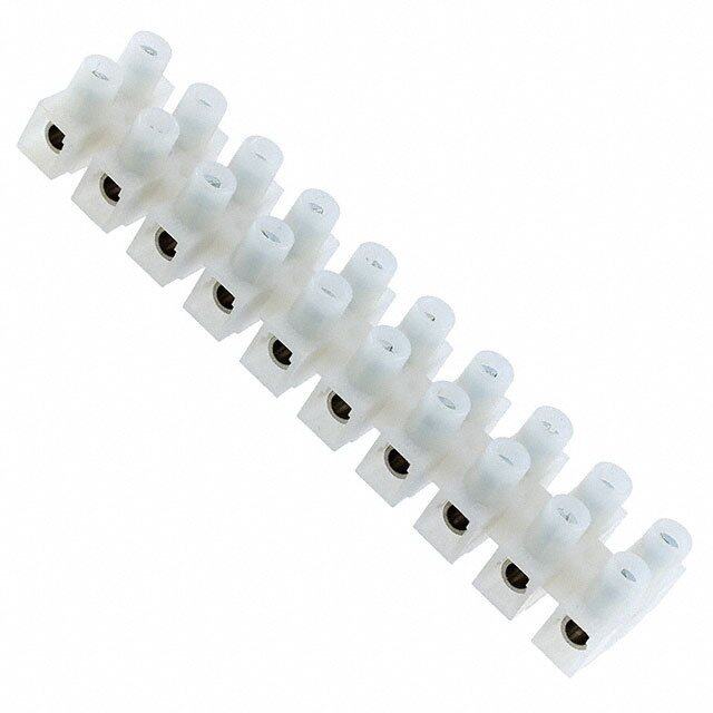
| 描述 | RES ARRAY 220 OHM 8 RES 16DIP电阻器网络与阵列 220ohms 16pin 2% M-DIP |
| 产品分类 | |
| 品牌 | Vishay / DaleVishay Dale |
| 产品手册 | |
| 产品图片 |
|
| rohs | RoHS 合规性豁免无铅 / 符合限制有害物质指令(RoHS)规范要求 |
| 产品系列 | 电阻器网络与阵列,Vishay / Dale MDP1603220RGE04MDP |
| 数据手册 | |
| 产品型号 | MDP1603220RGE04MDP1603220RGE04 |
| 产品种类 | 电阻器网络与阵列 |
| 产品类型 | Networks |
| 供应商器件封装 | 16-DIP |
| 其它名称 | MDP1603220RGE04-ND |
| 包装 | 管件 |
| 商标 | Vishay / Dale |
| 外壳宽度 | 7.87 mm |
| 外壳长度 | 19.05 mm |
| 外壳高度 | 3.05 mm |
| 大小/尺寸 | 0.850" 长 x 0.250" 宽(21.59mm x 6.35mm) |
| 安装类型 | 通孔 |
| 容差 | ±2%2 % |
| 封装/外壳 | 16-DIP(0.300",7.62mm) |
| 工作温度 | -55°C ~ 125°C |
| 工作温度范围 | - 55 C to + 125 C |
| 应用 | - |
| 引线间隔 | 2.54 mm |
| 引脚数 | 16 |
| 标准包装 | 25 |
| 每元件功率 | 0.25 W (1/4 W)250mW |
| 温度系数 | 100 PPM / C±100ppm/°C |
| 电路类型 | 隔离Isolated |
| 电阻(Ω) | 220 |
| 电阻器数 | 8 |
| 电阻器数量 | 8 |
| 电阻数值 | 220 Ohms |
| 端接类型 | DIP |
| 管脚数量 | 16 |
| 系列 | MDP |
| 高度 | 0.155"(3.94mm) |


- 商务部:美国ITC正式对集成电路等产品启动337调查
- 曝三星4nm工艺存在良率问题 高通将骁龙8 Gen1或转产台积电
- 太阳诱电将投资9.5亿元在常州建新厂生产MLCC 预计2023年完工
- 英特尔发布欧洲新工厂建设计划 深化IDM 2.0 战略
- 台积电先进制程称霸业界 有大客户加持明年业绩稳了
- 达到5530亿美元!SIA预计今年全球半导体销售额将创下新高
- 英特尔拟将自动驾驶子公司Mobileye上市 估值或超500亿美元
- 三星加码芯片和SET,合并消费电子和移动部门,撤换高东真等 CEO
- 三星电子宣布重大人事变动 还合并消费电子和移动部门
- 海关总署:前11个月进口集成电路产品价值2.52万亿元 增长14.8%
_renders/IS42S16800F-7BLI.jpg)


PDF Datasheet 数据手册内容提取
MDP 01, 03, 05 Vishay Dale Thick Film Resistor Networks, Dual-In-Line, Molded DIP, 01, 03, 05 Schematics FEATURES • 0.160" [4.06 mm] maximum seated height and rugged, molded case construction Available • Thick film resistive elements • Low temperature coefficient (- 55 °C to + 125 °C) e1 ± 100 ppm/°C • Reduces total assembly costs RoHS* • Compatible with automatic insertingþequipment COMPLIANT • Wide resistance range (10 Ω to 2.2 MΩ) • Uniform performance characteristics • Available in tube pack • Lead (Pb)-free version is RoHS compliant STANDARD ELECTRICAL SPECIFICATIONS GLOBAL SCHEMATIC RESISTOR RESISTANCE STANDARD TEMPERATURE TCR WEIGHT MODEL/ POWER RATING RANGE TOLERANCE COEFFICIENT TRACKING** NO. OF Max. AT 70 °C (- 55 °C to + 125 °C) (- 55 °C to + 125 °C) PINS W Ω ± % ppm/°C ppm/°C g 01 0.125 10 - 2.2M ± 50 MDP 14 03 0.250 10 - 2.2M ± 2 (± 1, ± 5)*** ± 100 ± 50 1.3 05 0.125 Consult factory ± 100 01 0.125 10 - 2.2M ± 50 MDP 16 03 0.250 10 - 2.2M ± 2 (± 1, ± 5)*** ± 100 ± 50 1.5 05 0.125 Consult factory ± 100 * For resistor power ratings at + 25 °C see derating curves ** Tighter tracking available *** ± 1 % and ± 5 % tolerences available on request GLOBAL PART NUMBER INFORMATION New Global Part Numbering: MDP1403100RGD04 (preferred part numbering format) M D P 1 4 0 3 1 0 0 R G D 0 4 GLOBAL PIN COUNT SCHEMATIC RESISTANCE TOLERANCE PACKAGING SPECIAL MODEL VALUE CODE MDP 14 = 14 Pin 01 = Bussed R = Decimal F = ± 1 % E04 = Lead (Pb)-free, Tube Blank = Standard 16 = 16 Pin 03 = Isolated K =Thousand G = ± 2 % D04 = Tin/Lead,Tube (Dash Number) 00 = Special M = Million J = ± 5 % (up to 3 digits) 10R0 = 10 Ω S = Special From 1-999 680K = 680 k Ω as applicable 1M00 = 1.0 M Ω Historical Part Number example: MDP1403101G (will continue to be accepted) MDP 14 03 101 G D04 HISTORICAL PIN COUNT SCHEMATIC RESISTANCE TOLERANCE PACKAGING MODEL VALUE CODE New Global Part Numbering: MDP1405121CGD04 (preferred part numbering format) M D P 1 4 0 5 1 2 1 C G D 0 4 GLOBAL PIN COUNT SCHEMATIC RESISTANCE TOLERANCE PACKAGING SPECIAL MODEL VALUE CODE MDP 14 = 14 Pin 05 = Dual 3 digit F = ± 1 % E04 = Lead (Pb)-free, Tube Blank = Standard 16 = 16 Pin Terminator Impedance code G = ± 2 % D04 = Tin/Lead,Tube (Dash Number) followed by J = ± 5 % (up to 3 digits) Alpha modifier From 1-999 (see Impedence as applicable codes table) Historical Part Number example: MDP1405221271G (will continue to be accepted) MDP 14 05 221 271 G D04 HISTORICAL PIN COUNT SCHEMATIC RESISTANCE RESISTANCE TOLERANCE PACKAGING MODEL VALUE 1 VALUE 2 CODE * Pb containing terminations are not RoHS compliant, exemptions may apply www.vishay.com For technical questions contact: ff2aresistors@vishay.com Document Number: 31511 1 Revision: 28-Jul-06
MDP 01, 03, 05 Thick Film Resistor Networks, Dual-In-Line, Vishay Dale Molded DIP, 01, 03, 05 Schematics DIMENSIONS in inches [millimeters] 0.310± 0.010 A± 0.010 [0.254] [03..10250±± 00..102075] [7.87± 0.254] 0.250± 0.005 [6.35± 0.127] 0.030 Pin #1 [0.762] Typ. 0.010 + 0.005 IdentificatPioinn #1 [01.0.9705±± 00..308115] [00..405178±± 00..000736] 0[3.1.3300 ++- 000...300811105 [0.254 -+- 0 00.0..01502127] - 0.254] 0.100± 0.010 0.290 Min. [2.54± 0.254] B± 0.010 [0.254] 0.050± 0.005 00..332600 NMoamx.. Non-Accumulative Tol. [1.27± 0.127] [7.37 Min. "C" Spaces 8.13 Nom. 9.14 Max.] GLOBAL MODEL A B C MDP 14 0.750 [19.05] 0.600 [15.24] 6 MDP 16 0.850 [21.59] 0.700 [17.78] 7 TECHNICAL SPECIFICATIONS PARAMETER UNIT MDP14 MDP16 Package Power Rating (Maximum at + 70 °C) W 1.73 1.92 Voltage Coefficient of Resistance V < 50 ppm typical eff Dielectric Strength VAC 200 Insulation Resistance Ω > 10 000M minimum Operating Temperature Range °C - 55 to + 125 Storage Temperature Range °C - 55 to + 150 MECHANICAL SPECIFICATIONS Marking Resistance to Solvents: Permanency testing per MIL-STD-202, Method 215 Solderability: Per MIL-STD-202, Method 208E Body: Molded epoxy Terminals: Solder plated leads Weight: 14 pin = 1.3 grams; 16 pin = 1.5 grams Document Number: 31511 For technical questions contact: ff2aresistors@vishay.com www.vishay.com Revision: 28-Jul-06 2
MDP 01, 03, 05 Vishay Dale Thick Film Resistor Networks, Dual-In-Line, Molded DIP, 01, 03, 05 Schematics IMPEDANCE CODES CODE R1(Ω) R2(Ω) CODE R1(Ω) R2(Ω) 500B 82 130 141A 270 270 750B 120 200 181A 330 390 800C 130 210 191A 330 470 990A 160 260 221B 330 680 101C 180 240 281B 560 560 111C 180 270 381B 560 1.2K 121B 180 390 501C 620 2.7K 121C 220 270 102A 1.5K 3.3K 131A 220 330 202B 3K 6.2K CIRCUIT APPLICATIONS 01 SCHEMATIC 13 and 15 resistors with one pin common The MDPXX01 circuit provides a choice of 13 and 15 nominally equal • • • • • • • • resistors, each connected between a common pin (14 and 16) and a discrete PC board pin. Commonly used in the following applications: (cid:129) MOS/ROM Pull-up/Pull-down (cid:129) TTL Input Pull-down MDP1401 (cid:129) Open Collector Pull-up (cid:129) Digital Pulse Squaring Pin #1 MDP1601 (cid:129) "Wired OR" Pull-up (cid:129) TTL Unused Gate Pull-up (cid:129) Power Driven Pull-up (cid:129) High Speed Parallel Pull-up 03 SCHEMATIC 7 and 8 isolated resistors The MDPXX03 provides a choice of 7 and 8 nominally equal resistors, each resistor isolated from all others and wired directly across. Commonly used in the following applications: (cid:129) "Wired OR" Pull-up (cid:129) Long-line Impedance Balancing MDP1403 (cid:129) Power Driven Pull-up (cid:129) LED Current Limiting Pin #1 MDP1603 (cid:129) Powergate Pull-up (cid:129) ECL Output Pull-down (cid:129) Line Termination (cid:129) TTL Input Pull-down 05 SCHEMATIC TTL dual-line terminator; pulse squaring R1 R1 R1 R1 R1 R1 R1 The MDPXX05 circuit contains 12 and 14 series pair of resistors. R2 R2 R2 R2 R2 R2 R2 Each series pair is connected between ground and a common line. R1 R1 R1 R1 R1 R1 R1 The junction of these resistor pairs is connected to the input terminals. R2 R2 R2 R2 R2 R2 R2 The 05 circuits are designed for TTL dual-line termination and pulse squaring. MDP1405, MDP1605 Pin #1 Standard E-24 resistance values stocked. Consult factory www.vishay.com For technical questions contact: ff2aresistors@vishay.com Document Number: 31511 3 Revision: 28-Jul-06
MDP 01, 03, 05 Thick Film Resistor Networks, Dual-In-Line, Vishay Dale Molded DIP, 01, 03, 05 Schematics s) att W 16 Pin Package g ( 3.00 atin 2.70 14 Pin Package R er w o P Single Resistor 03 0.380 0.190 01 and 05 - 50 + 25 + 70 + 125 + 150 Derating Ambient Temperature °C PERFORMANCE MAX. ΔR TEST CONDITIONS (Typical Test Lots) 1.5 rated power, applied 1.5 hours “ON” and 0.5 hour “OFF” for 100 hours Power Conditioning ± 0.50 % ΔR ± 4 hours at + 25 °C ambient temperature Thermal Shock 5 cycles between - 65 °C and + 125 °C ± 0.50 % ΔR Short Time Overload 2.5 x rated working voltage 5 seconds ± 0.25 % ΔR Low Temperature Operation 45 minutes at full rated working voltage at - 65 °C ± 0.25 % ΔR Moisture Resistance 240 hours with humidity ranging from 80 % RH to 98 % RH ± 0.50 % ΔR Leads immersed in + 350 °C solder to within 1/16" of device body for Resistance to Soldering Heat ± 0.25 % ΔR 3 seconds Shock Total of 18 shocks at 100 G's ± 0.25 % ΔR Vibration 12 hours at maximum of 20 G's between 10 and 2000 Hz ± 0.25 % ΔR 1000 hours at + 70 °C, rated power applied 1.5 hours “ON, 0.5 hour “OFF” Load Life ± 1.00 % ΔR for full 1000 hour period. Derated according to the curve. Terminal Strength 4.5 pound pull for 30 seconds ± 0.25 % ΔR Insulation Resistance 10 000 Megohm (minimum) - Dielectric Withstanding Voltage No evidence of arcing or damage (200 VRMS for 1 minute) - Document Number: 31511 For technical questions contact: ff2aresistors@vishay.com www.vishay.com Revision: 28-Jul-06 4
Legal Disclaimer Notice Vishay Disclaimer All product specifications and data are subject to change without notice. Vishay Intertechnology, Inc., its affiliates, agents, and employees, and all persons acting on its or their behalf (collectively, “Vishay”), disclaim any and all liability for any errors, inaccuracies or incompleteness contained herein or in any other disclosure relating to any product. Vishay disclaims any and all liability arising out of the use or application of any product described herein or of any information provided herein to the maximum extent permitted by law. The product specifications do not expand or otherwise modify Vishay’s terms and conditions of purchase, including but not limited to the warranty expressed therein, which apply to these products. No license, express or implied, by estoppel or otherwise, to any intellectual property rights is granted by this document or by any conduct of Vishay. The products shown herein are not designed for use in medical, life-saving, or life-sustaining applications unless otherwise expressly indicated. Customers using or selling Vishay products not expressly indicated for use in such applications do so entirely at their own risk and agree to fully indemnify Vishay for any damages arising or resulting from such use or sale. Please contact authorized Vishay personnel to obtain written terms and conditions regarding products designed for such applications. Product names and markings noted herein may be trademarks of their respective owners. Document Number: 91000 www.vishay.com Revision: 18-Jul-08 1
Mouser Electronics Authorized Distributor Click to View Pricing, Inventory, Delivery & Lifecycle Information: V ishay: MDP1601150RGD04 MDP1401150RGD04 MDP1410470KGD04 MDP1601470KGD04 MDP16033K30GD04 MDP14033K30GD04 MDP16033K90GD04 MDP14033K90GD04 MDP140122K0GD04 MDP160122K0GD04 MDP160120K0GD04 MDP140120K0GD04 MDP160127K0GD04 MDP140127K0GD04 MDP1603270KGD04 MDP1601220RGD04 MDP1401220RGD04 MDP1601200RGD04 MDP1401200RGD04 MDP1401270RGD04 MDP1601270RGD04 MDP16015K10GD04 MDP14135K10GD04 MDP16015K60GD04 MDP14145K60GD04 MDP1405102AGD04 MDP1403100KGD04 MDP1603100KGD04 MDP1601560KGD04 MDP1401560KGD04 MDP141147R0GD04 MDP140168R0GD04 MDP140122R0GD04 MDP140127R0GD04 MDP140639R0GD04 MDP1603220KGD04 MDP140133R0GD04 MDP140151R0GD04 MDP1403220KGD04 MDP140156R0GD04 MDP140182R0GD04 MDP160347K0GD04 MDP140347K0GD04 MDP14013K90GD04 MDP14013K30GD04 MDP16013K30GD04 MDP16013K90GD04 MDP1605191AGD04 MDP1403680KGD04 MDP1603680KGD04 MDP1405390KGD04 MDP1601390KGD04 MDP1403150RGD04 MDP1603150RGD04 MDP160110K0GD04 MDP140110K0GD04 MDP1401680RGD04 MDP1601680RGD04 MDP1403330KGD04 MDP1603330KGD04 MDP1603820KGD04 MDP1603100RGD04 MDP1403100RGD04 MDP1403820KGD04 MDP1401120KGD04 MDP1403180RGD04 MDP1603180RGD04 MDP1601120KGD04 MDP1401150KGD04 MDP160168R0GD04 MDP1403220RGD04 MDP160182R0GD04 MDP160147R0GD04 MDP1403470KGD04 MDP1603470KGD04 MDP1603560RGD04 MDP1403560RGD04 MDP16011M00GD04 MDP14011K50GD04 MDP16011K00GD04 MDP16011K50GD04 MDP160375R0GD04 MDP160310R0GD04 MDP160333R0GD04 MDP160350R0GD04 MDP160347R0GD04 MDP160356R0GD04 MDP160351R0GD04 MDP160339R0GD04 MDP160382R0GD04 MDP16031K50GD04 MDP14031K50GD04 MDP16031K80GD04 MDP16031M00GD04 MDP14031K80GD04 MDP16031K00GD04 MDP160327R0GD04 MDP160322R0GD04 MDP16031K20GD04 MDP160368R0GD04