ICGOO在线商城 > MCR72-6G

 Datasheet下载
- 型号: MCR72-6G
- 制造商: ON Semiconductor
- 库位|库存: xxxx|xxxx
- 要求:
| 数量阶梯 | 香港交货 | 国内含税 |
| +xxxx | $xxxx | ¥xxxx |
查看当月历史价格
查看今年历史价格
MCR72-6G产品简介:
ICGOO电子元器件商城为您提供MCR72-6G由ON Semiconductor设计生产,在icgoo商城现货销售,并且可以通过原厂、代理商等渠道进行代购。 提供MCR72-6G价格参考以及ON SemiconductorMCR72-6G封装/规格参数等产品信息。 你可以下载MCR72-6G参考资料、Datasheet数据手册功能说明书, 资料中有MCR72-6G详细功能的应用电路图电压和使用方法及教程。
| 参数 | 数值 |
| 产品目录 | |
| 描述 | THYRISTOR SCR 8A 400V TO220ABSCR 400V 8A |
| 产品分类 | SCR - 单个分离式半导体 |
| GateTriggerCurrent-Igt | 0.2 mA |
| GateTriggerVoltage-Vgt | 1.5 V |
| 品牌 | ON Semiconductor |
| 产品手册 | |
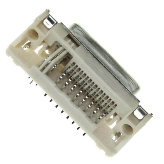
| 产品图片 |
|
| rohs | 符合RoHS无铅 / 符合限制有害物质指令(RoHS)规范要求 |
| 产品系列 | 晶体闸流管,SCR,ON Semiconductor MCR72-6G- |
| 数据手册 | |
| 产品型号 | MCR72-6G |
| SCR类型 | 灵敏栅极 |
| 不重复通态电流 | 100 A |
| 产品目录页面 | |
| 产品种类 | SCR |
| 供应商器件封装 | TO-220AB |
| 保持电流Ih最大值 | 6 mA |
| 关闭状态漏泄电流(在VDRMIDRM下) | 0.01 mA |
| 其它名称 | MCR72-6GOS |
| 包装 | 散装 |
| 商标 | ON Semiconductor |
| 安装类型 | 通孔 |
| 安装风格 | Through Hole |
| 封装 | Bulk |
| 封装/外壳 | TO-220-3 |
| 封装/箱体 | TO-220-3 |
| 工作温度 | -40°C ~ 110°C |
| 工厂包装数量 | 500 |
| 最大工作温度 | + 110 C |
| 最大栅极峰值反向电压 | 5 V |
| 最小工作温度 | - 40 C |
| 栅极触发电压-Vgt | 1.5 V |
| 栅极触发电流-Igt | 0.2 mA |
| 标准包装 | 500 |
| 正向电压下降 | 2 V |
| 电压-断态 | 400V |
| 电压-栅极触发(Vgt)(最大值) | 1.5V |
| 电压-通态(Vtm)(最大值) | 2V |
| 电流-不重复浪涌50、60Hz(Itsm) | 100A @ 60Hz |
| 电流-保持(Ih)(最大值) | 6mA |
| 电流-断态(最大值) | 10µA |
| 电流-栅极触发(Igt)(最大值) | 200µA |
| 电流-通态(It(AV))(最大值) | - |
| 电流-通态(It(RMS))(最大值) | 8A |
| 系列 | MCR72-6 |
| 额定重复关闭状态电压VDRM | 400 V |


PDF Datasheet 数据手册内容提取
Thyristors 8Amps Sen SCR MCR72-3, MCR72-6, MCR72-8 Pb Description Designed for industrial and consumer applications such as temperature, light and speed control; process and remote controls; warning systems; capacitive discharge circuits and MPU interface. Features • Center Gate Geometry for • Low Trigger Currents, 200 Uniform Current Density A Maximum for Direct • All Diffused and Glass- Driving from Integrated Passivated Junctions for Circuits Parameter Uniformity and • These are Pb−Free Stability Devices • Small, Rugged Thermowatt Construction for Low Thermal Resistance, High Heat Dissipation and Durability Pin Out Functional Diagram G A K 4 TO-220AB Case 221A Additional Information Style 4 1 2 3 Datasheet Resources Samples © 2020 Littelfuse, Inc. Specifications are subject to change without notice. Revised: 03/27/20
Thyristors 8Amps Sen SCR Maximum Ratings (T = 25°C unless otherwise noted) J Rating Symbol Value Unit MCR72-3 100 Peak Repetitive Off−State Voltage (Note 1) V , MCR72-6 DRM 400 V (− 40 to 110°C, Sine Wave, 50 to 60 Hz, Gate Open) V MCR72-8 RRM 600 On-State RMS Current I 8.0 A (180º Conduction Angles; T = 83ºC) T (RMS) C Peak Non-Repetitive Surge Current I 100 A (1/2 Cycle, Sine Wave 60 Hz, T = 110°C TSM J Circuit Fusing Consideration (t = 8.3 ms) I2t 40 A²s Forward Peak Gate Voltage (Pulse Width ≤ 10 µsec, T= 83°C) V ±5.0 V C GM Forward Peak Gate Current (Pulse Width ≤ 10 µsec, T= 83°C) I 1.0 A C GM Forward Peak Gate Power (Pulse Width ≤ 10 µsec, T= 83°C) P 5.0 W C GM Average Gate Power (t = 8.3 ms, T = 83ºC) P 0.75 W C G(AV) Operating Junction Temperature Range T -40 to +110 °C J Storage Temperature Range T -40 to +150 °C stg Mounting Torque − 8.0 in. lb. Stresses exceeding those listed in the Maximum Ratings table may damage the device. If any of these limits are exceeded, device functionality should not be assumed, damage may occur and reliability may be affected. 1. V and V for all types can be applied on a continuous basis. Ratings apply for zero or negative gate voltage; however, positive gate voltage shall not be applied concurrent with negative potential on the anode. Blocking voltages DRM RRM shall not be tested with a constant current source such that the voltage ratings of the devices are exceeded. Thermal Characteristics Characterstic Symbol Value Unit Thermal Resistance, Junction-to-Case R 2.2 ƟJC °C/W Thermal Resistance, Junction-to-Ambient R 60 ƟJA Maximum Lead Temperature for Soldering Purposes, 1/8” from T 260 °C case for 10 seconds L Electrical Characteristics - OFF (T = 25°C unless otherwise noted) J Characteristic Symbol Min Typ Max Unit Peak Repetitive Blocking Current TJ = 25°C IDRM - - 10 (VAK = VDRM = VRRM; RGK=1KΩ) TJ = 110°C IRRM - - 500 µA High Logic Level Supply Current from V I 4 4 - CC CCH Electrical Characteristics - ON (T = 25°C unless otherwise noted) J Characteristic Symbol Min Typ Max Unit Peak Forward On−State Voltage V _ 1.7 2.0 V (I = 16 A Peak, Pulse Width ≤ 1 ms, Duty Cycle ≤ 2%) TM TM Gate Trigger Current (Continuous dc) (Note 3) (V = 12 V; R = 100 Ω) I _ 30 200 µA D L GT Gate Trigger Voltage (Continuous dc) (Note 3) (V = 12 V; R = 100 Ω) V _ 0.5 1.5 V D L GT Gate Trigger Non-Trigger Voltage (V = 12 Vdc, R = 100 Ω, T = 110°C) V 0.1 _ _ V D L J GD Holding Current I _ _ 6.0 mA (V = 12 V, Initiating Current = 200 mA, RGK = 1kΩ) H D Gate Controlled Turn-On Time (Note 5) t _ 1.0 _ µs (V = Rated V , I = 16 A, I = 2 mA) gt D DRM TM G © 2020 Littelfuse, Inc. Specifications are subject to change without notice. Revised: 03/27/20
Thyristors 8Amps Sen SCR Dynamic Characteristics Characteristic Symbol Min Typ Max Unit Critical Rate−of−Rise of Off-State Voltage dv/dt - 10 − V/µs (V = Rated V , Exponential Waveform, Gate Open, T = 110°C) D DRM J Product parametric performance is indicated in the Electrical Characteristics for the listed test conditions, unless otherwise noted. Product performance may not be indicated by the Electrical Characteristics if operated under different conditions. 2. Ratings apply for negative gate voltage or R = 1KΩ. Devices shall not have a positive gate voltage concurrently with a negative voltage on the anode. Devices should not be tested with a constant current source for forward and GK reverse blocking capability such that the voltage applied exceeds the rated blocking voltage. 3. RGK current not included in measurement. Voltage Current Characteristic of SCR +Current Symbol Parameter V Quadrant 1 TM Main Terminal 2+ VDRM Peak Repetitive Forward Off State Voltage On State I I Peak Forward Blocking Current I at V H DRM RRM RRM V Peak Repetitive Reverse Off State Voltage RRM Off State +Voltage IRRM Peak Reverse Blocking Current IH IDRM at VDRM VTM Maximum On State Voltage QMuaaind Traenrmt 3inal 2- VTM I Holding Current H Figure 1. Average Current Derating Figure 2. On−State Power Dissipation s) 16 att W n ( dc o 12 pati α 180º si er Dis 8.0 α = Conduction Ang6l0ºe 90º w α = 30º o P e g 4.0 a er v A P, AV 0 0 2.0 4.0 6.0 8.0 I Average On-State Current (Amp) T(AV), Figure 3. Normalized Gate Current Figure 4. Gate Voltage © 2020 Littelfuse, Inc. Specifications are subject to change without notice. Revised: 03/27/20
Thyristors 8Amps Sen SCR Dimensions Part Marking System TO-220 TO-220 Case 221A-01 Case 221A-09 4 Issue O Issue AH SEATING TO-220AB PLANE Case 221A B F C Style 3 T S 1 4 2 Q A 4 3 4 12 3 U H TO-220AB Z K CaSsteyl 2e2 31A MYCMARKA7A2X-XxG CTaOSs-te2y2l 2e02 A31BA MCYRM7A2X-6XTG AKA L R V 1 J 1 2 G 3 23 D MCR72-x =Device Code MCR72-6T =Device Code Y =Year Y =Year N M =Month M =Month A =Assembly Site A =Assembly Site AKA =Diode Polarity AKA =Diode Polarity G =Pb-Free Package G =Pb-Free Package Inches Millimeters Dim Pin Assignment Min Max Min Max 1 Cathode A 0.590 0.620 14.99 15.75 2 Anode B 0.380 0.420 9.65 10.67 3 Gate C 0.178 0.188 4.52 4.78 4 Anode D 0.025 0.035 0.64 0.89 F 0.142 0.147 3.61 3.73 G 0.095 0.105 2.41 2.67 H 0.110 0.130 2.79 3.30 Ordering Information J 0.018 0.024 0.46 0.61 K 0.540 0.575 13.72 14.61 Device Package Shipping L 0.060 0.075 1.52 1.91 MCR72−3G N 0.195 0.205 4.95 5.21 MCR72−6G Q 0.105 0.115 2.67 2.92 TO−220AB MCR72−6TG 500 Units / Box (Pb−Free) R 0.085 0.095 2.16 2.41 MCR72−8G S 0.045 0.060 1.14 1.52 MCR72−8TG T 0.235 0.255 5.97 6.47 U 0.000 0.050 0.00 1.27 V 0.045 --- 1.15 --- Z --- 0.080 --- 2.04 1. DIMENSIONING AND TOLERANCING PER ANSI Y14.5M, 1982. 2. CONTROLLING DIMENSION: INCH. 3. DIMENSION Z DEFINES A ZONE WHERE ALL BODY AND LEAD IRREGULARITIES ARE ALLOWED. Disclaimer Notice - Information furnished is believed to be accurate and reliable. However, users should independently evaluate the suitability of and test each product selected for their own applications. Littelfuse products are not designed for, and may not be used in, all applications. Read complete Disclaimer Notice at http://www.littelfuse.com/disclaimer-electronics. © 2020 Littelfuse, Inc. Specifications are subject to change without notice. Revised: 03/27/20