ICGOO在线商城 > 集成电路(IC) > PMIC - 电池充电器 > MCP73837-FCI/UN

 Datasheet下载
- 型号: MCP73837-FCI/UN
- 制造商: Microchip
- 库位|库存: xxxx|xxxx
- 要求:
| 数量阶梯 | 香港交货 | 国内含税 |
| +xxxx | $xxxx | ¥xxxx |
查看当月历史价格
查看今年历史价格
MCP73837-FCI/UN产品简介:
ICGOO电子元器件商城为您提供MCP73837-FCI/UN由Microchip设计生产,在icgoo商城现货销售,并且可以通过原厂、代理商等渠道进行代购。 MCP73837-FCI/UN价格参考¥9.05-¥9.37。MicrochipMCP73837-FCI/UN封装/规格:PMIC - 电池充电器, Charger IC Lithium-Ion/Polymer 10-MSOP。您可以下载MCP73837-FCI/UN参考资料、Datasheet数据手册功能说明书,资料中有MCP73837-FCI/UN 详细功能的应用电路图电压和使用方法及教程。
| 参数 | 数值 |
| 产品目录 | 集成电路 (IC)半导体 |
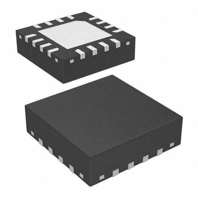
| 描述 | IC LIION CHRGR USB/AC-IN 10MSOP电池管理 1A USB/DC input auto-swich |
| 产品分类 | |
| 品牌 | Microchip Technology |
| 产品手册 | |
| 产品图片 |
|
| rohs | 符合RoHS无铅 / 符合限制有害物质指令(RoHS)规范要求 |
| 产品系列 | 电源管理 IC,电池管理,Microchip Technology MCP73837-FCI/UN- |
| 数据手册 | 点击此处下载产品Datasheethttp://www.microchip.com/mymicrochip/filehandler.aspx?ddocname=en533248 |
| 产品型号 | MCP73837-FCI/UN |
| 产品目录页面 | |
| 产品种类 | 电池管理 |
| 产品类型 | Charge Management |
| 供应商器件封装 | 10-MSOP |
| 其它名称 | MCP73837FCIUN |
| 功能 | 充电管理 |
| 包装 | 管件 |
| 商标 | Microchip Technology |
| 安装类型 | 表面贴装 |
| 安装风格 | SMD/SMT |
| 封装 | Tube |
| 封装/外壳 | 10-TFSOP,10-MSOP(0.118",3.00mm 宽) |
| 封装/箱体 | MSOP |
| 工作温度 | -40°C ~ 85°C |
| 工作电源电压 | 3.75 V to 6 V |
| 工厂包装数量 | 100 |
| 最大工作温度 | + 85 C |
| 最小工作温度 | - 40 C |
| 标准包装 | 100 |
| 电压-电源 | 4.5 V ~ 6 V |
| 电池化学 | 锂离子,锂聚合物 |
| 电池类型 | Li-Ion, Li-Poly |
| 输出电压 | 4.2 V, 4.35 V, 4.4 V, 4.5 V |
| 输出电流 | 1200 mA |


- 商务部:美国ITC正式对集成电路等产品启动337调查
- 曝三星4nm工艺存在良率问题 高通将骁龙8 Gen1或转产台积电
- 太阳诱电将投资9.5亿元在常州建新厂生产MLCC 预计2023年完工
- 英特尔发布欧洲新工厂建设计划 深化IDM 2.0 战略
- 台积电先进制程称霸业界 有大客户加持明年业绩稳了
- 达到5530亿美元!SIA预计今年全球半导体销售额将创下新高
- 英特尔拟将自动驾驶子公司Mobileye上市 估值或超500亿美元
- 三星加码芯片和SET,合并消费电子和移动部门,撤换高东真等 CEO
- 三星电子宣布重大人事变动 还合并消费电子和移动部门
- 海关总署:前11个月进口集成电路产品价值2.52万亿元 增长14.8%


PDF Datasheet 数据手册内容提取
MCP73837/8 Advanced Stand-Alone Li-Ion / Li-Polymer Battery Charge Management Controller with Autonomous AC-Adapter or USB-Port Source Selection Features Applications • High Accuracy Preset Voltage Regulation: + 0.5% • Smart Phones and Personal Data Assistants • Available Voltage Regulation Options: (PDA) - 4.20V, 4.35V, 4.4V, or 4.5V • Portable Media Players(PMP) • Complete Linear Charge Management Controller: • Ultra Mobile Devices(UMD) - Autonomous Power Source Selection • Digital Cameras - Integrated Pass Transistors • MP3 Players - Integrated Current Sense • Bluetooth Headsets - Integrated Reverse Discharge Protection • Handheld Medical Devices • Constant Current (CC) / Constant Voltage (CV) • AC/USB Dual Source Li-Ion Battery Chargers Operation with Thermal Regulation Description • Selectable USB-Port Charge Current: - Low: 1 Unit Load / High: 5 Unit Loads The MCP73837 and MCP73838 devices are fully • Programmable AC-Adapter Charge Current: integrated linear Li-Ion / Li-Polymer battery chargers - 15mA - 1000mA with autonomous power source selection. Along with its small physical size, the low number of external • Two Charge Status Outputs components required makes the MCP73837/8 ideally • Power-Good Monitor: MCP73837 suitable for portable applications. • Timer Enable: MCP73838 The MCP73837/8 automatically selects the USB-Port • Automatic Recharge: or AC-Adapter as the power source for the system. For - Selectable Voltage Threshold the USB-Port powered systems, the MCP73837/8 • Automatic End-of-Charge Control: specifically adheres to the current limits governed by - Selectable Charge Termination Current Ratio the USB specification. The host microcontroller can - Selectable Safety Timer Period select from two preset maximum charge current rates of 100mA (low power USB-port) or 500mA (high • Preconditioning of Deeply Depleted Cells - can be power USB-port). With an AC-Adapter providing power disabled to the system, an external resistor sets the magnitude • Battery Cell Temperature Monitor of the system or charge current up to a maximum of 1A. • UVLO (Undervoltage Lockout) The MCP73837/8 employs a constant current / • Automatic Power-Down when Input Power is constant voltage charge algorithm with selectable Removed preconditioning and charge termination. The constant • Low-Dropout (LDO) Linear Regulator Mode voltage regulation is fixed with four available options: • Numerous Selectable Options Available for a 4.20V, 4.35V, 4.40V, or 4.50V, to accommodated the Variety of Applications: new emerging battery charging requirements. The - Refer to Section1.0 “Electrical MCP73837/8 limits the charge current based on die Characteristics” for Selectable Options” temperature during high power or high ambient conditions. This thermal regulation optimizes the - Refer to the “Product Identification charge cycle time while maintaining the device System” for Standard Options reliability. • Temperature Range: -40°C to 85°C The MCP73837/8 are fully specified over the ambient • Packaging: temperature range of -40°C to +85°C. - 10-Lead 3mm x 3mm DFN The MCP73837/8 devices are available in a 10-Lead, - 10-Lead MSOP* 3mm x 3mm, DFN package or in a 10-Lead MSOP *Consult Factory for MSOP Package package. Availability. © 2007 Microchip Technology Inc. DS22071A-page 1
MCP73837/8 Package Types MCP73837/8 MCP73837/8 10-Lead DFN 3mm x 3mm 10-Lead MSOP VAC 1 10 VBAT VAC 1 10 VBAT VUSB 2 9 THERM VUSB 2 9 THERM STAT1 3 8 PG (TE) STAT1 3 8 PG (TE) STAT2 4 7 PROG2 STAT2 4 7 PROG2 VSS 5 6 PROG1 VSS 5 6 PROG1 Typical Applications MCP73837 Typical Application 1 10 Ac-dc Adapter VAC VBAT Thermsitor 4.7µF Single 4.7µF USB Port 2 VUSB THERM 9 LCie-Iloln 1kΩ 4.7µF 3 STAT1 VSS 5 1kΩ 4 7 STAT2 PROG2 Hi Low 1kΩ 8 6 PG PROG1 RPROG MCP73838 Typical Application 1 10 Ac-dc Adapter VAC VBAT Thermsitor 4.7µF 2 9 4.7µF USB Port VUSB THERM Cell 1 KΩ 4.7µF 3 8 STAT1 TE Hi Low 1 KΩ 4 7 STAT2 PROG2 Hi Low 5 6 VSS PROG1 RPROG DS22071A-page 2 © 2007 Microchip Technology Inc.
MCP73837/8 Functional Block Diagram (MCP73837/8) VOREG DIRECTION CONTROL 6µA VUSB VBAT SENSEFET G=0.001 100mA/500mA 10k 2k SENSEFET G=0.001 VOREG DIRECTION CONTROL VAC AC/USB CURRENT LIMIT + SENSEFET G=0.001 1k VREF - SENSEFET G=0.001 PROG1 AC/USB CA + REFERENCE, VREF (1.21V) BIAS, UVLO, - AND SHDN 111k 310k 10k VOREG UVLO + 72.7k - - 470.6k PRECONDITION + TERM 48k PROG2 - + CHARGE CHARGE 6k STAT1 CONTROL, + VA TIMER, AND 157.3k - STAT2 SLOTAGTICUS VOREG + LDO - 175k PG (TE) + 50µA HTVT - 470.6k THERM + LTVT - 175k 121k 1M VSS © 2007 Microchip Technology Inc. DS22071A-page 3
MCP73837/8 1.0 ELECTRICAL † Notice: Stresses above those listed under “Maximum Ratings” may cause permanent damage to the device. This is CHARACTERISTICS a stress rating only and functional operation of the device at those or any other conditions above those indicated in the Absolute Maximum Ratings† operational listings of this specification is not implied. Exposure to maximum rating conditions for extended periods VDDN................................................................................7.0V may affect device reliability. All Inputs and Outputs w.r.t. V ...............-0.3 to (V +0.3)V SS DD Maximum Junction Temperature, T ............Internally Limited J Storage temperature.....................................-65°C to +150°C ESD protection on all pins Human Body Model (1.5kW in Series with 100pF)......≥ 4kV Machine Model (200pF, No Series Resistance).............300V DC CHARACTERISTICS Electrical Specifications: Unless otherwise indicated, all limits apply for V = [V (typical) + 0.3V] to 6V, DD REG T = -40°C to +85°C. Typical values are at +25°C, V = [V (typical) + 1.0V] A DD REG Parameters Sym Min Typ Max Units Conditions Supply Input Supply Voltage V V (Typ) — 6 V Note1 DD REG +0.3V Supply Current I — 1900 3000 µA Charging SS 110 300 µA Charge Complete, No Battery — 75 100 µA Standby (PROG Floating) — 0.6 5 µA Shutdown (V < V - DD BAT 100mV or V < V ) DD STOP UVLO Start Threshold V 3.35 3.45 3.55 V V = Low to High (USB-Port) START DD UVLO Stop Threshold V 3.25 3.35 3.45 V V = High to Low (USB-Port) STOP DD UVLO Hysteresis V — 75 — mV (USB-Port) HYS UVLO Start Threshold V 4.1 4.15 4.3 V (AC-Adapter) START UVLO Stop Threshold V 4.0 4.1 4.2 V (AC-Adapter) STOP UVLO Hysteresis V — 55 — mV (AC-Adapter) HYS Voltage Regulation (Constant Voltage Mode) Regulated Charge Voltage V 4.179 4.20 4.221 V V =[V (typical)+1V] REG DD REG 4.328 4.35 4.372 V I =30mA OUT 4.378 4.40 4.422 V T =-5°C to +55°C A 4.477 4.50 4.523 V Regulated Charge Voltage Tolerance V -0.5 — +0.5 % T =-5°C to +55°C RTOL A Line Regulation |(ΔV / — 0.075 0.2 %/V V =[V (typical)+1V] to 6V BAT DD REG V )/ΔV | I =30mA BAT DD OUT Load Regulation |ΔV /V | — 0.150 0.3 % I =10mA to 100mA BAT BAT OUT V =[V (typical)+1V] DD REG Supply Ripple Attenuation PSRR — 60 — dB I =10mA, 10Hz to 1kHz OUT — 52 — dB I =10mA, 10Hz to 10kHz OUT — 23 — dB I =10mA, 10Hz to 1MHz OUT Current Regulation (Fast Charge Constant-Current Mode) AC-Adapter Fast Charge Current I 95 105 115 mA PROG1 = 10kΩ REG 900 1000 1100 mA PROG1 = 1kΩ, Note2 T =-5°C to +55°C A Note 1: The supply voltage (V ) = V when input power source is from Ac-Adapter and the supply voltage (V ) = V DD AC DD USB when input power source is from USB-Port. 2: The value is guaranteed by design and not production tested. 3: The current is based on the ratio of selected current regulation (I ). REG 4: The maximum charge impedance has to be less than shutdown impedance for normal operation. DS22071A-page 4 © 2007 Microchip Technology Inc.
MCP73837/8 DC CHARACTERISTICS (Continued) Electrical Specifications: Unless otherwise indicated, all limits apply for V = [V (typical) + 0.3V] to 6V, DD REG T = -40°C to +85°C. Typical values are at +25°C, V = [V (typical) + 1.0V] A DD REG Parameters Sym Min Typ Max Units Conditions USB-Port Fast Charge Current I 80 90 100 mA PROG2 = Low REG 400 450 500 mA PROG2 = High T =-5°C to +55°C A Maximum Output Current Limit I — 1200 — mA PROG1 < 833Ω MAX Precondition Current Regulation (Trickle Charge Constant-Current Mode) Precondition Current Ratio I / I 7.5 10 12.5 % Note3 PREG REG 15 20 25 % T =-5°C to +55°C A 30 40 50 % 100 % Precondition Current Threshold Ratio V / V 64 66.5 69 % V Low to High PTH REG BAT 69 71.5 74 % Precondition Hysteresis V — 120 — mV V High to Low PHYS BAT Charge Termination Charge Termination Current Ratio I / I 3.75 5 6.25 % PROG1 = 1kΩ to 10kΩ TERM REG 5.6 7.5 9.4 % T =-5°C to +55°C A 7.5 10 12.5 % Note3 15 20 25 % Automatic Recharge Recharge Voltage Threshold Ratio V / V 92 94.0 96 % V High to Low RTH REG BAT 95 97 99 % T =-5°C to +55°C A Pass Transistor ON-Resistance ON-Resistance R — 350 — mΩ V = 4.5V, T = 105°C DSON DD J Battery Discharge Current Output Reverse Leakage Current I — 0.1 2 µA Standby (PROG1 or PROG2 DISCHARGE Floating) — 0.55 2 µA Shutdown (V < V - DD BAT 100mV or V < V ) DD STOP — -6 -15 µA Charge Complete Status Indicators - STAT1, STAT2, PG (MCP73837) Sink Current I — 16 35 mA SINK Low Output Voltage V — 0.3 1 V I = 4mA OL SINK Input Leakage Current I — 0.03 1 µA High Impedance, V on pin LK DD PROG1 Input (PROG1) Charge Impedance Range R 1 — — kΩ Note4 PROG Shutdown Impedance R 70 — 200 kΩ Minimum Impedance for PROG Shutdown PROG2 Inputs (PROG2) Input High Voltage Level V 0.8V — — % IH DD Input Low Voltage Level V — — 0.2V % IL DD Shutdown Voltage Level V 0.2V — 0.8V % SD DD DD Input Leakage Current I — 7 15 µA V = V LK PROG2 DD Note 1: The supply voltage (V ) = V when input power source is from Ac-Adapter and the supply voltage (V ) = V DD AC DD USB when input power source is from USB-Port. 2: The value is guaranteed by design and not production tested. 3: The current is based on the ratio of selected current regulation (I ). REG 4: The maximum charge impedance has to be less than shutdown impedance for normal operation. © 2007 Microchip Technology Inc. DS22071A-page 5
MCP73837/8 DC CHARACTERISTICS (Continued) Electrical Specifications: Unless otherwise indicated, all limits apply for V = [V (typical) + 0.3V] to 6V, DD REG T = -40°C to +85°C. Typical values are at +25°C, V = [V (typical) + 1.0V] A DD REG Parameters Sym Min Typ Max Units Conditions Timer Enable (TE) Input High Voltage Level V 2 — — V IH Input Low Voltage Level V — — 0.8 V IL Input Leakage Current I — 0.01 1 µA V = V LK TE DD Thermistor Bias Thermistor Current Source I 47 50 53 µA 2kΩ < R < 50kΩ THERM THERM Thermistor Comparator Upper Trip Threshold V 1.20 1.23 1.26 V V Low to High T1 T1 Upper Trip Point Hysteresis V — -40 — mV T1HYS Lower Trip Threshold V 0.235 0.250 0.265 V V High to Low T2 T2 Lower Trip Point Hysteresis V — 40 — mV T2HYS System Test (LDO) Mode Input High Voltage Level V — — V - 0.1 V IH DD THERM Input Sink Current I 3 5.5 20 µA Stand-by Or System Test SINK Mode Bypass Capacitance C 1 — — µF I < 250mA BAT OUT 4.7 µF I > 250mA OUT Automatic Power Down (SLEEP Comparator, Direction Control) Automatic Power Down Entry V V + V + — V 2.3V < V < V PD BAT BAT BAT REG Threshold 10mV 100mV V Falling DD Automatic Power Down Exit Threshold V - V + V + V 2.3V < V < V PDEXIT BAT BAT BAT REG 150mV 250mV V Rising DD Thermal Shutdown Die Temperature T — 150 — °C SD Die Temperature Hysteresis T — 10 — °C SDHYS Note 1: The supply voltage (V ) = V when input power source is from Ac-Adapter and the supply voltage (V ) = V DD AC DD USB when input power source is from USB-Port. 2: The value is guaranteed by design and not production tested. 3: The current is based on the ratio of selected current regulation (I ). REG 4: The maximum charge impedance has to be less than shutdown impedance for normal operation. DS22071A-page 6 © 2007 Microchip Technology Inc.
MCP73837/8 AC CHARACTERISTICS Electrical Specifications: Unless otherwise indicated, all limits apply for V = [V (typical) + 0.3V] to 6V. DD REG Typical values are at +25°C, V = [V (typical) + 1.0V] DD REG Parameters Sym Min Typ Max Units Conditions UVLO Start Delay t — — 5 ms V Low to High START DD Current Regulation Transition Time Out of Precondition t — — 10 ms V < V to V > V DELAY BAT PTH BAT PTH Current Rise Time Out of Precondition t — — 10 ms I Rising to 90% of I RISE OUT REG Precondition Comparator Filter Time t 0.4 1.3 3.2 ms Average V Rise/Fall PRECON BAT Termination Comparator Filter Time t 0.4 1.3 3.2 ms Average I Falling TERM OUT Charge Comparator Filter Time t 0.4 1.3 3.2 ms Average V Falling CHARGE BAT Thermistor Comparator Filter Time t 0.4 1.3 3.2 ms Average THERM Rise/Fall THERM Elapsed Timer Elapsed Timer Period t 0 0 0 Hours Timer Disabled ELAPSED 3.6 4.0 4.4 Hours 5.4 6.0 6.6 Hours 7.2 8.0 8.8 Hours Status Indicators Status Output Turn-off t — — 500 µs I = 1mA to 0mA OFF SINK Status Output Turn-on t — — 500 µs I = 0mA to 1mA ON SINK TEMPERATURE SPECIFICATIONS Electrical Specifications: Unless otherwise indicated, all limits apply for V = [V (typ.) + 0.3V] to 6V. DD REG Typical values are at +25°C, V = [V (typ.) + 1.0V] DD REG Parameters Sym Min Typ Max Units Conditions Temperature Ranges Specified Temperature Range T -40 — +85 °C A Operating Temperature Range T -40 — +125 °C J Storage Temperature Range T -65 — +150 °C A Thermal Package Resistances Thermal Resistance, 10-Lead MSOP θ — 113 — °C/W 4-Layer JC51-7 Standard Board, JA Natural Convection. Note1 Thermal Resistance, 10-Lead 3mm x θ — 41 — °C/W 4-Layer JC51-7 Standard Board, JA 3mm DFN Natural Convection Note 1: This represents the minimum copper condition on the PCB ( Printed Circuit Board). © 2007 Microchip Technology Inc. DS22071A-page 7
MCP73837/8 2.0 TYPICAL PERFORMANCE CURVES Note: The graphs and tables provided following this note are a statistical summary based on a limited number of samples and are provided for informational purposes only. The performance characteristics listed herein are not tested or guaranteed. In some graphs or tables, the data presented may be outside the specified operating range (e.g., outside specified power supply range) and therefore outside the warranted range. Note: Unless otherwise indicated, V = [V (typical) + 1V], I = 30mA, and T = +25°C, Constant-voltage mode. DD REG OUT A 4.210 ation Voltage (V) 44444.....111228990050505 TEMP = 25°C IOUT = 50 mA IOIOUUTT = = 1 1000 mmAA ge Current (µA)112...260 VVDBDAT = = F 4lo.2aVting Regul 44..117850 IOUT = 500 mA Leaka0.8 ery 4.170 put 0.4 Batt 4.165 IOUT = 1000 mA Out0.0 4.160 -40 -30 -20 -10 0 10 20 30 40 50 60 70 80 4.5 4.8 5.0 5.3 5.5 5.8 6.0 Supply Voltage (V) Temperature (°C) FIGURE 2-1: Battery Regulation Voltage FIGURE 2-4: Output Leakage Current (V ) vs. Supply Voltage (V ). (I ) vs. Ambient Temperature (T ). BAT DD DISCHARGE A age (V)44..220150 IOUT = 10 mA IOUT = 50 mA VDD = 5.2V nt (µA) 112...680 VTEDDM =P F =l o+a2t5in°Cg n Volt44..129050 IOUT = 100 mA Curre 11..24 ulatio4.190 IOUT = 500 mA kage 01..80 Reg4.185 IOUT = 1000 mA Lea 0.6 y 4.180 ut 0.4 Batter44..117705 Outp 00..02 3.0 3.1 3.2 3.3 3.4 3.5 3.6 3.7 3.8 3.9 4.0 4.1 4.2 -40-30-20-10 0 10 20 30 40 50 60 70 80 Ambient Temperature (°C) Battery Voltage (V) FIGURE 2-2: Battery Regulation Voltage FIGURE 2-5: Output Leakage Current (V ) vs. Ambient Temperature (T ). (I ) vs. Battery Voltage (V ). BAT A DISCHARGE BAT 0.50 1000 nt (µA) 000...344505 TEMVPD D= = 2 V5 B°ACT 789000000 VTeDDm =p 5=. 22V5°C akage Curre 0000....12235050 I (mA)REG 345600000000 Le 0.10 200 ut 0.05 100 utp 0.00 0 O 3.0 3.1 3.2 3.3 3.4 3.5 3.6 3.7 3.8 3.9 4.0 4.1 4.2 1 6 11 16 21 26 31 36 41 46 51 56 61 Battery Voltage (V) R (kΩ) PROG FIGURE 2-3: Output Leakage Current FIGURE 2-6: Charge Current (I ) vs. OUT (I ) vs. Battery Regulation Voltage Programming Resistor (R ). DISCHARGE PROG (V ). BAT DS22071A-page 8 © 2007 Microchip Technology Inc.
MCP73837/8 Note: Unless otherwise indicated, V = [V (typical) + 1V], I = 30mA and T = +25°C, Constant-voltage mode. DD REG OUT A 1200 110 1150 RPROG = 1 kΩ 108 RPROG = 10 kΩ A)1100 Temp = +25°C A) 106 VDD = 5.2V harge Current (m11008899050505000000 harge Current (m 111000999024468 C C 750 92 700 90 4.5 4.8 5.0 5.3 5.5 5.8 6.0 -40-30-20-10 0 10 20 30 40 50 60 70 80 Supply Voltage (V) Ambient Temperature (°C) FIGURE 2-7: Charge Current (I ) vs. FIGURE 2-10: Charge Current (I ) vs. OUT OUT Supply Voltage (V ). Ambient Temperature (T ). DD A 55 104 A)102 RTePmROpG == +102 5k°ΩC mA) 5534 RVDPDR O=G 5=. 22V0 kΩ harge Current (m109990468 Charge Current ( 444555789012 C 92 46 90 45 4.5 4.8 5.0 5.3 5.5 5.8 6.0 -40 -30 -20 -10 0 10 20 30 40 50 60 70 80 Supply Voltage (V) Ambient Temperature (°C) FIGURE 2-8: Charge Current (I ) vs. FIGURE 2-11: Charge Current (I ) vs. OUT OUT Supply Voltage (V ). Ambient Temperature (T ). DD A 1100 1200 A)1050 RVDPDR O=G 5=. 21V kΩ A) 11010000 RPROG = 1 kΩ m1000 m 900 ent ( 950 ent ( 780000 urr 900 urr 600 C C 500 ge 850 ge 400 ar 800 ar 300 Ch Ch 200 750 100 700 0 5 5 5 5 5 5 5 5 5 5 5 5 5 5 -40-30-20-10 0 10 20 30 40 50 60 70 80 2 3 4 5 6 7 8 9 0 1 2 3 4 5 1 1 1 1 1 1 Ambient Temperature (°C) Junction Temperature (°C) FIGURE 2-9: Charge Current (I ) vs. FIGURE 2-12: Charge Current (I ) vs. OUT OUT Ambient Temperature (T ). Junction Temperature (T ). A J © 2007 Microchip Technology Inc. DS22071A-page 9
MCP73837/8 Note: Unless otherwise indicated, V = [V (typical) + 1V], I = 30mA and T = +25°C, Constant-voltage mode. DD REG OUT A 600 550 RPROG = 2 kΩ 52.0 A) 500 A)51.5 VDD = 5.2V m 450 m51.0 Current ( 233450500000 Current (455900...505 Charge 11205050000 hermistor 44447889....5050 0 T 47.0 5 5 5 5 5 5 5 5 5 5 5 5 5 5 2 3 4 5 6 7 8 9 0 1 2 3 4 5 0 0 0 0 0 0 0 0 0 0 0 0 0 0 1 1 1 1 1 1 4 3 2 1 1 2 3 4 5 6 7 8 9 - - - - Junction Temperature (°C) Ambient Temperature (°C) FIGURE 2-13: Charge Current (I ) vs. FIGURE 2-16: Thermistor Current (I ) OUT THERM Junction Temperature (T ). vs. Ambient Temperature (T ). J A 120 0 110 RPROG = 10 kΩ IOUT = 10 mA A)100 -10 COUT = 4.7 µF ent (m 789000 n (dB)--3200 Curr 5600 uatio-40 Charge 234000 Atten--6500 10 0 -70 25 35 45 55 65 75 85 95 05 15 25 35 45 55 0.01 0.1 1 10 100 1000 1 1 1 1 1 1 Junction Temperature (°C) Frequency (kHz) FIGURE 2-14: Charge Current (I ) vs. FIGURE 2-17: Power Supply Ripple OUT Junction Temperature (T ). Rejection (PSRR). J 52.0 0 or Current (mA) 445555990011......050505 Temp = +25°C nuation (dB) ----43210000 ICOOUUT T= = 1 40.07 mµFA mist 48.5 Atte -50 er 48.0 -60 h 47.5 T 47.0 -70 4.5 4.8 5.0 5.3 5.5 5.8 6.0 0.01 0.1 1 10 100 1000 Supply Voltage (V) Frequency (kHz) FIGURE 2-15: Thermistor Current (I ) FIGURE 2-18: Power Supply Ripple THERM vs. Supply Voltage (V ). Rejection (PSRR). DD DS22071A-page 10 © 2007 Microchip Technology Inc.
MCP73837/8 Note: Unless otherwise indicated, V = [V (typical) + 1V], I = 30mA and T = +25°C, Constant-voltage mode. DD REG OUT A 16 0.1 1 0.1 Input Source (V)111024468 ----00000....4321 Output Ripple (V) Output Current (A) -0000000000..........10123456789 IOUT = 100 mA ------00000000.0......3212105555 Output Ripple (V) 2 4 4 0 4 4 4 4 3 3 3 3 0-200IO-100UT = 1000 m100A T200ime300 (µs400) 500 600 700 -0.5 -4.0E-0 -2.0E-0 0.0E+0 2.0E-0Tim4.0E-0e (M6.0E-0inu8.0E-0tes)1.0E-0 1.2E-0 1.4E-0 1.6E-0 FIGURE 2-19: Line Transient Response. FIGURE 2-22: Load Transient Response. 16 0.1 14 0 V) 12 V) ce ( 10 -0.1 ple ( our 8 -0.2 Rip ut S 6 -0.3 put Inp 4 -0.4 Out 2 IOUT = 10 mA 0 -0.5 -200 -100 0 100 200 300 400 500 600 700 800 Time (µs) FIGURE 2-20: Line Transient Response. FIGURE 2-23: V UVLO Start Delay AC (I = 1A). OUT 0.35 0.04 A) 0.3 IOUT = 10 mA 0.02 V) ent ( 0.02.25 -00.02 ple ( Output Curr 00..001.5150 ----0000....1000864 Output Rip -0.05 -0.12 -4.0E-04 -2.0E-04 0.0E+00 2.0E-04 4.0E-04 6.0E-04 8.0E-04 1.0E-03 1.2E-03 1.4E-03 1.6E-03 Time (Minutes) FIGURE 2-21: Load Transient Response. FIGURE 2-24: V UVLO Start Delay USB (USB = Low). © 2007 Microchip Technology Inc. DS22071A-page 11
MCP73837/8 Note: Unless otherwise indicated, V = [V (typical) + 1V], I = 30mA and T = +25°C, Constant-voltage mode. DD REG OUT A UVLOVAC 5.0 0.12 V)4.0 0.1 A) ge ( 0.08 nt ( olta3.0 0.06 urre V C y 2.0 e Batter1.0 VRDPDR O=G 5=. 2UVSB_Low 00..0024 Charg 180 mAh Li-Ion Battery 0.0 0 0 20 40 60 80 100120140160180 Time (Minutes) FIGURE 2-25: V UVLO Start Delay FIGURE 2-28: Complete Charge Cycle USB (USB = High) (180mAh Li-Ion Battery). 5.0 1.2 5.0 0.12 C.C. Begins V)4.0 1 A) V)4.0 0.1 A) Voltage (3.0 00..68 Current ( Voltage (3.0 C.V. Begins 00..0068 Current ( Battery 12..00 VR12DP0DR O0=G m 5=.A 21hV k LΩi-Ion Battery 00..24 Charge Battery 12..00 Preconditioning VR18DP0DR O =mG 5A=. h2UV LSiB-Io_Lno Bwattery 00..0024 Charge 0.0 0 0.0 0 0000000000000000 123456789012345 0 1 2 3 4 5 6 7 8 9 10 111111 Time (Minutes) Time (Minutes) FIGURE 2-26: Complete Charge Cycle FIGURE 2-29: Typical Charge Profile in (1200mAh Li-Ion Battery). Preconditioning and CC-CV (180mAh Li-Ion Battery). 4.5 1.2 4.0 V) 3.5 0.9 A) oltage ( 23..50 0.6 urrent ( V 2.0 C y e atter 11..05 VDD = 5.2V 0.3 harg B RPROG = 1 kΩ C 0.5 1200 mAh Li-Ion Battery 0.0 0 0 1 2 3 4 5 6 7 8 9 10 Time (Minutes) FIGURE 2-27: Typical Charge Profile in Thermal Regulation (1200mAh Li-Ion Battery). DS22071A-page 12 © 2007 Microchip Technology Inc.
MCP73837/8 3.0 PIN DESCRIPTION The descriptions of the pins are listed in Table3-1. TABLE 3-1: PIN FUNCTION TABLES Pin Number Symbol I/O Function MSOP-10 DFN-10 1 1 V I AC-Adapter Supply Input AC 2 2 V I USB-Port Supply Input USB 3 3 STAT1 O Charge Status Output 1 (Open-Drain) 4 4 STAT2 O Charge Status Output 2 (Open-Drain) 5 5 V — Battery Management 0V Reference SS 6 6 PROG1 I/O Current Regulation Setting With AC-Adapter; Device Charge Control Enable; Precondition Set Point for AC control 7 7 PROG2 I Current Regulation Setting With USB-Port; Precondition Set Point for USB control. 8 8 PG O Available on MCP73837: Power-Good Status Output (Open-Drain) 8 8 TE I Available on MCP73838: Timer Enable; Enables Safety Timer (Active Low) 9 9 THERM I/O Thermistor Monitoring Input and Bias current; System Test (LDO) Mode Input 10 10 V I/O Battery Positive Input and Output Connection BAT — EP V — EP (Exposed Thermal Pad); There is an internal electrical SS connection between the exposed thermal pad and V . The EP SS must be connected to the same potential as the V pin on the SS Printed Circuit Board (PCB). 3.1 AC-Adapter Supply Input (V ) 3.5 Battery Management 0V Reference AC (V ) A supply voltage of V + 0.3V to 6V from ac-dc wall- SS REG adapter is recommended. When both the AC-Adapter Connect to negative terminal of battery and input and the USB-Port supply voltages are present at same supply. time, the AC-Adapter dominates the regulated charge current with the maximum value of 1A. Bypass to VSS 3.6 Battery Charge Control Output with a minimum of 4.7µF is recommended. (V ) BAT 3.2 USB-Port Supply Input (V ) Connect to the positive terminal of Li-Ion / Li-Polymer USB batteries. Bypass to V with a minimum of 1µF to SS A supply voltage of V + 0.3V to 6V from USB-Port is REG ensure loop stability when the battery is disconnected. recommended. When no supply voltage from V pin is AC available, the Li-Ion battery is charged directly from 3.7 AC-Adapter Current Regulation USB-Port. Bypass to V with a minimum of 1µF is SS Set (PROG1) recommended. The AC-Adapter constant charge current is set by 3.3 Charge Status Output 1 (STAT1) placing a resistor from PROG1 to V . PROG1 is the SS set point of precondition and termination when the AC- STAT1 is an open-drain logic output for connection to a Adapter is present. LED for charge status indication. Alternatively, a pull-up resistor can be applied for interfacing to a host micro- PROG1 also functions as device charge control controller. enable. The MCP73837/8 is shut down when an impedance value greater than 70kΩ is applied to 3.4 Charge Status Output 2 (STAT2) PROG1. When PROG1 is floating, the MCP73837/8 enters stand-by mode. STAT2 is an open-drain logic output for connection to a LED for charge status indication. Alternatively, a pull-up resistor can be applied for interfacing to a host microcontroller. © 2007 Microchip Technology Inc. DS22071A-page 13
MCP73837/8 3.8 USB-Port Current Regulation Set 3.10 Timer Enable (TE) (PROG2) Timer Enable (TE) is available only on MCP73838. The MCP73837/8 USB-Port current regulation set (TE) enables the built-in safety timer when pull low and input (PROG2) is a digital input selection. A logic Low disables the built-in safety timer when pull high. selects a 1 unit load charge current; a logic High selects Note: The built-in safety timer is available for both a 5 unit loads charge current. MCP73837 and MCP73838 in the following PROG2 also functions as the set point of precondition options: Disable, 4 HR, 6 HR, and 8 HR. and termination when USB-Port is present. When PROG2 is floating, the MCP73837/8 enters in stand-by 3.11 Battery Temperature Monitor mode. (THERM) 3.9 Power Good (PG) MCP73837/8 continuously monitors the battery temperature during a charge cycle by measuring the Power Good (PG) is available only on MCP73837. PG voltage between the THERM and V pins. An internal SS is an open-drain logic output for connection to a LED 50µA current source provides the bias for the most for input power supply indication. Alternatively, a pull- common 10kΩ negative-temperature coefficient up resistor can be applied for interfacing to a host thermistors (NTC). microcontroller. DS22071A-page 14 © 2007 Microchip Technology Inc.
MCP73837/8 4.0 DEVICE OVERVIEW The MCP73837/8 devices are simple, yet fully integrated linear charge management controllers. Figure4-1 depicts the operational flow algorithm. SHUTDOWN MODE* * Continuously Monitored VDD < VBAT -100mV VDD < V STOP STAT1 = Hi-Z STAT2 = Hi-Z PG = Hi-Z SYSTEM TEST (LDO) MODE STANDBY MODE * VTHERM > (VDD -100mV) VBAT > (VREG+100mV) STAT1 = LOW PROG > 200 kΩ STAT2 = LOW STAT1 = Hi-Z PG = LOW STAT2 = Hi-Z Timer Suspended PG = LOW V < V BAT PTH PRECONDITIONING MODE Charge Current = I PREG STAT1 = LOW STAT2 = Hi-Z PG = LOW Timer Reset V > V BAT PTH TEMPERATURE FAULT FAST CHARGE MODE V > V TIMER FAULT No Charge Current Charge Current = I REG BAT PTH No Charge Current STAT1 = Hi-Z STAT1 = LOW Timer Expired STAT1 = Hi-Z STAT2 = Hi-Z STAT2 = Hi-Z V < V STAT2 = Hi-Z PG = LOW PG = LOW BAT RTH PG = LOW Timer Suspended Timer Enabled Timer Suspended V = V BAT REG CONSTANT VOLTAGE MODE Charge Voltage = V REG STAT1 = LOW STAT2 = Hi-Z PG = LOW I < I BAT TERM Timer Expired CHARGE COMPLETE MODE No Charge Current STAT1 = Hi-Z STAT2 = LOW PG = LOW FIGURE 4-1: Flow Chart. © 2007 Microchip Technology Inc. DS22071A-page 15
MCP73837/8 4.1 Undervoltage Lockout (UVLO) In this mode, the MCP73837/8 supplies a percentage of the charge current (established with the value of the An internal undervoltage lockout (UVLO) circuit resistor connected to the PROG pin) to the battery. The monitors the input voltage and keeps the charger in percentage or ratio of the current is factory set. Refer to shutdown mode until the input supply rises above the Section1.0 “Electrical Characteristics” for UVLO threshold. The UVLO circuitry has a built-in preconditioning current options. hysteresis of 75mV for the USB-Port and 55mV for the AC-Adapter. When the voltage at the VBAT pin rises above the preconditioning threshold, the MCP73837/8 enters the In the event a battery is present when the input power constant current or fast charge mode. is applied, the input supply must rise 100mV above the battery voltage before MCP73837/8 becomes 4.5 Constant Current MODE - Fast operational. Charge The UVLO circuit places the device in shutdown mode if the input supply falls to within +100mV of the battery During the constant current mode, the programmed voltage. (AC-Adapter) or selected (USB-Port) charge current is supplied to the battery or load. The UVLO circuit is always active. At any time the input supply is below the UVLO threshold or within +100mV For AC-Adapter, the charge current is established of the voltage at the VBAT pin, the MCP73837/8 is using a single resistor from PROG to VSS. The placed in a shutdown mode. program resistor and the charge current are calculated using the following equation: During any UVLO condition, the battery reverse discharge current shall be less than 2µA. EQUATION 4-1: 4.2 AUTONOMOUS POWER SOURCE SELECTION I = -1---0---0---0----V--- REG R PROG The MCP73837/8 devices are designed to select the USB-port or the AC-Adapter as the power source automatically. If the AC-Adapter input is not present, where RPROG is in kilo-ohms (kΩ) and IREG is in the USB-Port is selected. If both inputs are available, milliampers (mA). the AC-Adapter has first priority. When charging from a USB-Port, the host microcontroller has the option of selecting either a one Note: If the input power is switched during a unit load or a five unit loads charge rate based on the charge cycle, the power path switch-over PROG2 input. A logic LOW selects a one unit load shall be a break-before-make connection. charge rate, a HIGH selects a five unit loads charge As a result, the charge current can rate, and high impedance input suspends or disables momentarily go to zero. The charge cycle charging. timer shall remain continuous. Note: USB Specification Rev. 2.0 defines the 4.3 Charge Qualification maximum absolute current for one unit load is 100mA. This value is not an aver- For a charge cycle to begin, all UVLO conditions must age over time and shall not be exceed. be met and a battery or output load must be present. Constant current mode is maintained until the voltage A charge current programming resistor must be con- at the V pin reaches the regulation voltage, V ., nected from PROG1 to V . If the PROG1 or PROG2 BAT REG SS when constant current mode is invoked, the internal pin are open or floating, the MCP73837/8 is disabled timer is reset. and the battery reverse discharge current is less than 2µA. In this manner, the PROG1 pin acts as a charge 4.5.1 TIMER EXPIRED DURING enable and can be used as a manual shutdown. CONSTANT CURRENT - FAST CHARGE MODE 4.4 Preconditioning If the internal timer expires before the recharge voltage If the voltage at the VBAT pin is less than the threshold is reached, a timer fault is indicated and the preconditioning threshold, the MCP73837/8 enters a charge cycle terminates. The MCP73837/8 remains in preconditioning mode. The preconditioning threshold is this condition until the battery is removed, the input factory set. Refer to Section1.0 “Electrical battery is removed or the PROG1/2 pin is opened. If the Characteristics” for preconditioning threshold battery is removed or the PROG1/2 pin is opened, the options. MCP73837/8 enters the Stand-by mode where it remains until a battery is reinserted or the PROG1/2 pin DS22071A-page 16 © 2007 Microchip Technology Inc.
MCP73837/8 is reconnected. If the input power is removed, the 4.9 Thermal Regulation MCP73837/8 is in Shutdown. When the input power is reapplied, a normal start-up sequence ensues. The MCP73837/8 limits the charge current based on the die temperature. The thermal regulation optimizes the charge cycle time while maintaining device 4.6 Constant Voltage Mode reliability. Figure4-2 depicts the thermal regulation for When the voltage at the V pin reaches the the MCP73837/8. Refer to Section1.0 “Electrical BAT regulation voltage, V , constant voltage regulation Characteristics” for thermal package resistances and REG begins. The regulation voltage is factory set to 4.20V, Section6.1.1.2 “Thermal Considerations” for 4.35V, 4.40V, or 4.5V with a tolerance of ± 0.5%. calculating power dissipation. . 4.7 Charge Termination 1200 The charge cycle is terminated when, during constant 1100 RPROG = 1 kΩ 1000 voltage mode, the average charge current diminishes A)900 b(eeslotawb lais pheerdc ewnittha gthee o vf athluee p orfo tghrea mremsiesdto cr hcaorngnee ccuterrde ntot ent (m780000 the PROG pin) or the internal timer has expired. A 1ms Curr600 e 500 filter time on the termination comparator ensures that arg400 transient load conditions do not result in premature Ch300 charge cycle termination. The percentage or ratio of the 200 100 current is factory set. The timer period is factory set and 0 can be disabled. Refer to Section1.0 “Electrical 25 35 45 55 65 75 85 95 105 115 125 135 145 155 Characteristics” for charge termination current ratio Junction Temperature (°C) and timer period options. FIGURE 4-2: Thermal Regulation. The charge current is latched off and the MCP73837/8 enters a charge complete mode. 4.10 Thermal Shutdown 4.8 Automatic Recharge The MCP73837/8 suspends charge if the die temperature exceeds 150°C. Charging will resume The MCP73837/8 continuously monitors the voltage at when the die temperature has cooled by the VBAT pin in the charge complete mode. If the approximately 10°C. The thermal shutdown is a voltage drops below the recharge threshold, another secondary safety feature in the event that there is a charge cycle begins and current is once again supplied failure within the thermal regulation circuitry. to the battery or load. The recharge threshold is factory set. Refer to Section1.0 “Electrical Characteristics” for recharge threshold options. Note: Charge termination and automatic recharge features avoid constant charging Li-Ion batteries to prolong the life of Li-Ion batteries while keeping their capacity at healthy level. © 2007 Microchip Technology Inc. DS22071A-page 17
MCP73837/8 5.0 DETAILED DESCRIPTION at the THERM pin to factory set thresholds of 1.20V and 0.25V, typically. Once a voltage outside the thresholds is detected during a charge cycle, the 5.1 Analog Circuitry MCP73837/8 immediately suspends the charge cycle. 5.1.1 BATTERY MANAGEMENT INPUT The MCP73837/8 suspends charge by turning off the SUPPLY (V ) pass transistor and holding the timer value. The charge DD cycle resumes when the voltage at the THERM pin The V input is the input supply to the MCP73837/8. DD returns to the normal range. The MCP73837/8 can be supplied by either AC- Adapter (V ) or USB-Port (V ) with autonomous If temperature monitoring is not required, place a AC USB source selection. The MCP73837/8 automatically standard 10kΩ resistor from THERM to VSS. enters a Power-down mode if the voltage on the V DD 5.1.5 SYSTEM TEST (LDO) MODE input falls to within +100mV of the battery voltage or below the UVLO voltage (VSTOP). This feature prevents The MCP73837/8 can be placed in a system test mode. draining the battery pack when both the VAC and VUSB In this mode, the MCP73837/8 operates as a low drop- supplies are not present. out linear regulator (LDO). The output voltage is regulated to the factory set voltage regulation option. 5.1.2 AC-ADAPTER CURRENT The available output current is limited to the pro- REGULATION SET (PROG1) grammed fast charge current. For stability, the V BAT For the MCP73837/8, the charge current regulation output must be bypassed to VSS with a minimum can be scaled by placing a programming resistor capacitance of 1µF for output currents up to 250mA. (R ) from the PROG input to V . The program A minimum capacitance of 4.7µF is required for output PROG SS resistor and the charge current are calculated using currents above 250mA. the following equation: The system test mode is entered by driving the THERM input greater than (VDD - 100mV) with no battery EQUATION 5-1: connected to the output. In this mode, the MCP73837/ 8 can be used to power the system without a battery 1000V I = ----------------- being present. REG R PROG Where: Note1: ITHERM is disabled during shutdown, R = kilo-ohms (kΩ) stand-by, and system test modes. PROG I = milli-ampere (mA) 2: A pull-down current source on the REG THERM input is active only in stand-by and system test modes. The preconditioning current and the charge termination current are ratiometric to the fast charge 3: During system test mode, the PROG current based on the selected device options. input sets the available output current limit. 5.1.3 BATTERY CHARGE CONTROL 4: System test mode shall be exited by OUTPUT (V ) BAT releasing the THERM input or cycling The battery charge control output is the drain terminal input power. of an internal P-channel MOSFET. The MCP73837/8 5.2 Digital Circuitry provides constant current and voltage regulation to the battery pack by controlling this MOSFET in the linear 5.2.1 STATUS INDICATORS AND POWER region. The battery charge control output should be connected to the positive terminal of the battery pack. GOOD (PG) OPTION The charge status outputs have two different states: 5.1.4 TEMPERATURE QUALIFICATION Low (L), and High Impedance (Hi-Z). The charge status (THERM) outputs can be used to illuminate LEDs. Optionally, the The MCP73837/8 continuously monitors battery charge status outputs can be used as an interface to a temperature during a charge cycle by measuring the host microcontroller. Table5-1 summarizes the state of voltage between the THERM and the VSS pins. An the status outputs during a charge cycle. internal 50µA current source provides the bias for the most common 10kΩ negative-temperature coefficient (NTC) or positive-temperature coefficient (PTC) thermistors. The current source is controlled, avoiding measurement sensitivity to fluctuations in the supply voltage (V ). The MCP73837/8 compares the voltage DD DS22071A-page 18 © 2007 Microchip Technology Inc.
MCP73837/8 5.2.2 USB-PORT CURRENT 5.2.4 TIMER ENABLE (TE) OPTION REGULATION SELECT (PROG2) The timer enable (TE) input option is used to enable or For the MCP73837/8, driving the PROG2 input to a disable the internal timer. A low signal on this pin logic Low selects the low charge current setting enables the internal timer and a high signal disables (maximum 100mA). Driving the PROG2 input to a logic the internal timer. The TE input can be used to disable High selects the high charge current setting (maximum the timer when the charger is supplying current to 500mA). charge the battery and power the system load. The TE input is compatible with 1.8V logic. The TE option is TABLE 5-1: STATUS OUTPUTS available only on MCP73838. CHARGE CYCLE STATE STAT1 STAT2 PG 5.2.5 DEVICE DISABLE (PROG1/2) Shutdown Hi-Z Hi-Z Hi-Z The current regulation set input pin (PROG1/2) can be Standby Hi-Z Hi-Z L used to terminate a charge at any time during the Preconditioning L Hi-Z L charge cycle, as well as to initiate a charge cycle or to Constant Current L Hi-Z L initiate a recharge cycle. Placing a programming Constant Voltage L Hi-Z L resistor from the PROG1/2 input to VSS enables the device. Allowing the PROG1/2 input to float or applying Charge Complete - Standby Hi-Z L L a logic-high input signal, disables the device and Temperature Fault Hi-Z Hi-Z L terminates a charge cycle. When disabled, the device’s Timer Fault Hi-Z Hi-Z L supply current is reduced to 75µA, typically. System Test Mode L L L 5.2.3 POWER GOOD (PG) OPTION The power good (PG) option is a pseudo open-drain output. The PG output can sink current, but not source current. However, there is a diode path back to the input, and as such, the output should be pulled up only to the input. The PG output is low whenever the input to the MCP73837 is above the UVLO threshold and greater than the battery voltage. If the supply voltage is above the UVLO, but below V (typical)+0.3V, the REG MCP73837 will pulse the PG output as the device determines if a battery is present. The PG option is available only on MCP73837. © 2007 Microchip Technology Inc. DS22071A-page 19
MCP73837/8 6.0 APPLICATIONS Lithium-Polymer cells Constant-current followed by Constant-voltage. Figure6-1 depicts a typical stand- The MCP73837/8 devices are designed to operate in alone MCP73837 application circuit, while Figure6-2 conjunction with a host microcontroller or in stand- and Figure6-3 depict the accompanying charge alone applications. The MCP73837/8 devices provide profile. the preferred charge algorithm for Lithium-Ion and 1 10 V V AC BAT Thermsitor C OUT Single USB Port 2 V THERM 9 Li-Ion C USB Cell IN1 RWEAGLLU LCAUTBEED CIN2 1 ΚΩ 3 STAT1 VSS 5 1 ΚΩ 4 7 STAT2 PROG2 Hi Low 1 ΚΩ 8 6 /PG PROG1 R MCP73837 PROG FIGURE 6-1: MCP73837 Typical Stand-Alone Application Circuit. 6.1 Application Circuit Design 5.0 1.2 Due to the low efficiency of linear charging, the most 1 important factors are thermal design and cost, which V) 4.0 A) oltage ( 3.0 00..68 urrent ( aaanrnedd a tth hdeeir raemmcta bflu ieinmnctpt iceoodnoa olninf ctgeh eab irien. tpTwuhete ev wno lottarhsgete- c,b aoasutettep sruyitt u ccahutariorrengn eitsr, V C Battery 12..00 VRDPDR O=G 5=. 21V kΩ 00..24 Charge wPthrhiesec nso intudatihttiieoo nni,n dtghe mev iocbdeae tt etorhy at hsce h Cartorganensrts ahitnaiots nC etuodr rdeisnfstr oimpmao tdee tt.hh Inee 1200 mAh Li-Ion Battery 0.0 0 maximum power. A trade-off must be made between 0000000000000000 the charge current, cost, and thermal requirements of 123456789012345 111111 the charger. Time (Minutes) FIGURE 6-2: Typical Charge Profile 6.1.1 COMPONENT SELECTION (1200mAh Li-Ion Battery). Selection of the external components in Figure6-1 is crucial to the integrity and reliability of the charging system. The following discussion is intended as a guide 4.5 1.2 for the component selection process. 4.0 V) 3.5 0.9 A) 6.1.1.1 Charge Current Voltage ( 223...050 0.6 Current ( Tshhoeu pldr eafelwrraeyds f afostll ocwha rrgeefe creunrrceenst faonr dL igthuiuidman-Icoen cfreolmls attery 11..05 VDD = 5.2V 0.3 harge b7a0t0temryA m faansut fachctaurrgeer sc. uFrroern t efxoar map l1e0, 0p0rmogArah mLmi-Iionng B 0.5 R12P0RO0G m =A 1h k LΩi-Ion Battery C battery pack if its preferred fast charge rate is 0.7C. 0.0 0 This will result the shortest charge cycle time without 0 1 2 3 4 5 6 7 8 9 10 degradation a battery's life and performance. Time (Minutes) 6.1.1.2 Thermal Considerations FIGURE 6-3: Typical Charge Profile in The worst-case power dissipation in the battery Thermal Regulation (1200mAh Li-Ion Battery). charger occurs when the input voltage is at the maximum and the device has transitioned from the Preconditioning mode to the Constant-current mode. In this case, the power dissipation is: DS22071A-page 20 © 2007 Microchip Technology Inc.
MCP73837/8 EQUATION 6-1: Placing a programming resistor from the PROG1 input to V or driving PROG2 to logic High or Low enables SS PowerDissipation = (V –V )×I DDMAX PTHMIN REGMAX the device. Allowing either the PROG1 or PROG2 input Where: float disables the device and terminates a charge cycle. When disabled, the device’s supply current is reduced VDDMAX = the maximum input voltage to 75µA, typically. I = the maximum fast charge current REGMAX 6.1.1.6 Temperature Monitoring V = the minimum transition threshold PTHMIN voltage The charge temperature window can be set by placing fixed value resistors in series-parallel with a thermistor. The resistance values of RT1 and RT2 can be calculated For example, power dissipation with a 5V, ±10% input with the following equations in order to set the voltage source and 500mA, ±10% fast charge current temperature window of interest. is: For NTC thermistors: EXAMPLE 6-1: EQUATION 6-2: PowerDissipation = (5.5V–2.7V)×550mA = 1.54W R ×R 24kΩ= R +----T---2-------------C---O----L---D--- T1 R +R T2 COLD This power dissipation with the battery charger in the R ×R MSOP-10 package will cause thermal regulation to be 5kΩ= R +----T---2-------------H----O---T-- entered as depicted in Figure6-3. Alternatively, the T1 R +R T2 HOT 3mm x 3mm DFN package could be utilized to reduce Where: the charge cycle times. R = the fixed series resistance T1 6.1.1.3 External Capacitors R = the fixed parallel resistance T2 The MCP73837/8 is stable with or without a battery R the thermistor resistance at the COLD load. In order to maintain good AC stability in the lower temperature of interest Constant Voltage mode, a minimum capacitance of R = the thermistor resistance at the HOT 1µF is recommended to bypass the VBAT pin to VSS. upper temperature of interest This capacitance provides compensation when there is no battery load. In addition, the battery and For example, by utilizing a 10kΩ at 25°C NTC interconnections appear inductive at high frequencies. thermistor with a sensitivity index, β, of 3892, the These elements are in the control feedback loop during charge temperature range can be set to 0°C - 50°C by Constant Voltage mode. Therefore, the bypass placing a 1.54kΩ resistor in series (R ), and a capacitance may be necessary to compensate for the T1 69.8kΩ resistor in parallel (R ) with the thermistor. inductive nature of the battery pack. T2 Virtually any good quality output filter capacitor can be 6.1.1.7 Charge Status Interface used, independent of the capacitor’s minimum A status output provides information on the state of Effective Series Resistance (ESR) value. The actual charge. The output can be used to illuminate external value of the capacitor (and its associated ESR) LEDs or interface to a host microcontroller. Refer to depends on the output load current. A 1µF ceramic, Figure5-1 for a summary of the state of the status tantalum, or aluminum electrolytic capacitor at the output during a charge cycle. output is usually sufficient to ensure stability for output currents up to 500mA. 6.2 PCB Layout Issues 6.1.1.4 Reverse-Blocking Protection For optimum voltage regulation, place the battery pack The MCP73837/8 provides protection from a faulted or as close as possible to the device’s VBAT and VSS pins, shorted input. Without the protection, a faulted or recommended to minimize voltage drops along the shorted input would discharge the battery pack through high current-carrying PCB traces. the body diode of the internal pass transistor. If the PCB layout is used as a heatsink, adding many vias in the heatsink pad can help conduct more heat to 6.1.1.5 Charge Inhibit the backplane of the PCB, thus reducing the maximum The current regulation set input pin (PROG1/2) can be junction temperature. used to terminate a charge at any time during the charge cycle, as well as to initiate a charge cycle or initiate a recharge cycle. © 2007 Microchip Technology Inc. DS22071A-page 21
MCP73837/8 7.0 PACKAGING INFORMATION 7.1 Package Marking Information 10-Lead DFN Example: Marking Marking Part Number * Part Number * 1 10 Code Code 1 10 XXXX BABA 2 9 MCP73837-FCI/MF BABA MCP73837T-FCI/MF BABA 2 9 XYWW 0748 3 8 MCP73837-FJI/MF BABB MCP73837T-FJI/MF BABB 3 8 NNN 256 4 7 4 7 MCP73837-NVI/MF BABC MCP73837T-NVI/MF BABC 5 6 5 6 MCP73838-FCI/MF BACA MCP73838T-FCI/MF BACA MCP73838-FJI/MF BACB MCP73838T-FJI/MF BACB MCP73838-NVI/MF BACC MCP73838T-NVI/MF BACC * Consult Factory for Alternative Device Options. 10-Lead MSOP * * Example: Marking Marking Part Number * Part Number * Code Code MCP73837-FCI/UN 837FCI MCP73837T-FCI/UN 837FCI XXXXXX 837FCI MCP73837-FJI/UN 837FJI MCP73837T-FJI/UN 837FJI YWWNNN MCP73837-NVI/UN 837NVI MCP73837T-NVI/UN 837NVI 748256 MCP73838-FCI/UN 838FCI MCP73838T-FCI/UN 838FCI MCP73838-FJI/UN 838FJI MCP73838T-FJII/UN 838FJI MCP73838-NVI/UN 838NVI MCP73838T-NVI/UN 838NVI * Consult Factory for Alternative Device Options. * * Consult Factory for MSOP Package Availability. Legend: XX...X Customer-specific information Y Year code (last digit of calendar year) YY Year code (last 2 digits of calendar year) WW Week code (week of January 1 is week ‘01’) NNN Alphanumeric traceability code e3 Pb-free JEDEC designator for Matte Tin (Sn) * This package is Pb-free. The Pb-free JEDEC designator ( e 3 ) can be found on the outer packaging for this package. Note: In the event the full Microchip part number cannot be marked on one line, it will be carried over to the next line, thus limiting the number of available characters for customer-specific information. DS22071A-page 22 © 2007 Microchip Technology Inc.
MCP73837/8 (cid:2)(cid:3)(cid:4)(cid:5)(cid:6)(cid:7)(cid:8)(cid:9)(cid:10)(cid:11)(cid:7)(cid:12)(cid:13)(cid:14)(cid:15)(cid:9)(cid:16)(cid:17)(cid:7)(cid:11)(cid:9)(cid:18)(cid:11)(cid:7)(cid:13)(cid:19)(cid:9)(cid:20)(cid:21)(cid:9)(cid:5)(cid:6)(cid:7)(cid:8)(cid:9)(cid:10)(cid:7)(cid:15)(cid:22)(cid:7)(cid:23)(cid:6)(cid:9)(cid:24)(cid:25)(cid:18)(cid:26)(cid:9)(cid:27)(cid:9)(cid:28)(cid:29)(cid:28)(cid:29)(cid:3)(cid:30)(cid:31)(cid:9) (cid:9)!(cid:21)(cid:8)"(cid:9)#(cid:16)(cid:18)(cid:20)$ (cid:20)(cid:21)(cid:13)(cid:6)% -(cid:23)(cid:18)(cid:7)(cid:17)(cid:26)(cid:14)(cid:7)(cid:19)(cid:23)(cid:9)(cid:17)(cid:7)(cid:24)(cid:10)(cid:18)(cid:18)(cid:14)(cid:6)(cid:17)(cid:7)(cid:30)(cid:11)(cid:24)(cid:28)(cid:11)(cid:29)(cid:14)(cid:7)(cid:13)(cid:18)(cid:11)(cid:25)(cid:5)(cid:6)(cid:29)(cid:9)(cid:21)(cid:7)(cid:30)(cid:12)(cid:14)(cid:11)(cid:9)(cid:14)(cid:7)(cid:9)(cid:14)(cid:14)(cid:7)(cid:17)(cid:26)(cid:14)(cid:7)$(cid:5)(cid:24)(cid:18)(cid:23)(cid:24)(cid:26)(cid:5)(cid:30)(cid:7)(cid:4)(cid:11)(cid:24)(cid:28)(cid:11)(cid:29)(cid:5)(cid:6)(cid:29)(cid:7)#(cid:30)(cid:14)(cid:24)(cid:5)(cid:16)(cid:5)(cid:24)(cid:11)(cid:17)(cid:5)(cid:23)(cid:6)(cid:7)(cid:12)(cid:23)(cid:24)(cid:11)(cid:17)(cid:14)(cid:13)(cid:7)(cid:11)(cid:17)(cid:7) (cid:26)(cid:17)(cid:17)(cid:30)*..(cid:25)(cid:25)(cid:25)(cid:3)(cid:19)(cid:5)(cid:24)(cid:18)(cid:23)(cid:24)(cid:26)(cid:5)(cid:30)(cid:3)(cid:24)(cid:23)(cid:19).(cid:30)(cid:11)(cid:24)(cid:28)(cid:11)(cid:29)(cid:5)(cid:6)(cid:29) D e b N N L K E E2 EXPOSED PAD NOTE1 NOTE1 1 2 2 1 D2 TOPVIEW BOTTOMVIEW A A3 A1 NOTE2 /(cid:6)(cid:5)(cid:17)(cid:9) $0110$%+%,# !(cid:5)(cid:19)(cid:14)(cid:6)(cid:9)(cid:5)(cid:23)(cid:6)(cid:7)1(cid:5)(cid:19)(cid:5)(cid:17)(cid:9) $02 23$ $"4 2(cid:10)(cid:19)(cid:22)(cid:14)(cid:18)(cid:7)(cid:23)(cid:16)(cid:7)(cid:4)(cid:5)(cid:6)(cid:9) 2 (cid:2)5 (cid:4)(cid:5)(cid:17)(cid:24)(cid:26) (cid:14) 5(cid:3)’5(cid:7)(#) 3(cid:8)(cid:14)(cid:18)(cid:11)(cid:12)(cid:12)(cid:7)6(cid:14)(cid:5)(cid:29)(cid:26)(cid:17) " 5(cid:3)75 5(cid:3)85 (cid:2)(cid:3)55 #(cid:17)(cid:11)(cid:6)(cid:13)(cid:23)(cid:16)(cid:16)(cid:7) "(cid:2) 5(cid:3)55 5(cid:3)5(cid:27) 5(cid:3)5’ )(cid:23)(cid:6)(cid:17)(cid:11)(cid:24)(cid:17)(cid:7)+(cid:26)(cid:5)(cid:24)(cid:28)(cid:6)(cid:14)(cid:9)(cid:9) "(cid:31) 5(cid:3)(cid:27)5(cid:7),%- 3(cid:8)(cid:14)(cid:18)(cid:11)(cid:12)(cid:12)(cid:7)1(cid:14)(cid:6)(cid:29)(cid:17)(cid:26) ! (cid:31)(cid:3)55(cid:7)(#) %(cid:15)(cid:30)(cid:23)(cid:9)(cid:14)(cid:13)(cid:7)(cid:4)(cid:11)(cid:13)(cid:7)1(cid:14)(cid:6)(cid:29)(cid:17)(cid:26) !(cid:27) (cid:27)(cid:3)(cid:27)5 (cid:27)(cid:3)(cid:31)’ (cid:27)(cid:3) 7 3(cid:8)(cid:14)(cid:18)(cid:11)(cid:12)(cid:12)(cid:7)9(cid:5)(cid:13)(cid:17)(cid:26) % (cid:31)(cid:3)55(cid:7)(#) %(cid:15)(cid:30)(cid:23)(cid:9)(cid:14)(cid:13)(cid:7)(cid:4)(cid:11)(cid:13)(cid:7)9(cid:5)(cid:13)(cid:17)(cid:26) %(cid:27) (cid:2)(cid:3) 5 (cid:2)(cid:3)’7 (cid:2)(cid:3):’ )(cid:23)(cid:6)(cid:17)(cid:11)(cid:24)(cid:17)(cid:7)9(cid:5)(cid:13)(cid:17)(cid:26) (cid:22) 5(cid:3)(cid:2)7 5(cid:3)(cid:27)’ 5(cid:3)(cid:31)5 )(cid:23)(cid:6)(cid:17)(cid:11)(cid:24)(cid:17)(cid:7)1(cid:14)(cid:6)(cid:29)(cid:17)(cid:26) 1 5(cid:3)(cid:31)5 5(cid:3) 5 5(cid:3)’5 )(cid:23)(cid:6)(cid:17)(cid:11)(cid:24)(cid:17);(cid:17)(cid:23);%(cid:15)(cid:30)(cid:23)(cid:9)(cid:14)(cid:13)(cid:7)(cid:4)(cid:11)(cid:13) < 5(cid:3)(cid:27)5 = = (cid:20)(cid:21)(cid:13)(cid:6)(cid:12)% (cid:2)(cid:3) (cid:4)(cid:5)(cid:6)(cid:7)(cid:2)(cid:7)(cid:8)(cid:5)(cid:9)(cid:10)(cid:11)(cid:12)(cid:7)(cid:5)(cid:6)(cid:13)(cid:14)(cid:15)(cid:7)(cid:16)(cid:14)(cid:11)(cid:17)(cid:10)(cid:18)(cid:14)(cid:7)(cid:19)(cid:11)(cid:20)(cid:7)(cid:8)(cid:11)(cid:18)(cid:20)(cid:21)(cid:7)(cid:22)(cid:10)(cid:17)(cid:7)(cid:19)(cid:10)(cid:9)(cid:17)(cid:7)(cid:22)(cid:14)(cid:7)(cid:12)(cid:23)(cid:24)(cid:11)(cid:17)(cid:14)(cid:13)(cid:7)(cid:25)(cid:5)(cid:17)(cid:26)(cid:5)(cid:6)(cid:7)(cid:17)(cid:26)(cid:14)(cid:7)(cid:26)(cid:11)(cid:17)(cid:24)(cid:26)(cid:14)(cid:13)(cid:7)(cid:11)(cid:18)(cid:14)(cid:11)(cid:3) (cid:27)(cid:3) (cid:4)(cid:11)(cid:24)(cid:28)(cid:11)(cid:29)(cid:14)(cid:7)(cid:19)(cid:11)(cid:20)(cid:7)(cid:26)(cid:11)(cid:8)(cid:14)(cid:7)(cid:23)(cid:6)(cid:14)(cid:7)(cid:23)(cid:18)(cid:7)(cid:19)(cid:23)(cid:18)(cid:14)(cid:7)(cid:14)(cid:15)(cid:30)(cid:23)(cid:9)(cid:14)(cid:13)(cid:7)(cid:17)(cid:5)(cid:14)(cid:7)(cid:22)(cid:11)(cid:18)(cid:9)(cid:7)(cid:11)(cid:17)(cid:7)(cid:14)(cid:6)(cid:13)(cid:9)(cid:3) (cid:31)(cid:3) (cid:4)(cid:11)(cid:24)(cid:28)(cid:11)(cid:29)(cid:14)(cid:7)(cid:5)(cid:9)(cid:7)(cid:9)(cid:11)(cid:25)(cid:7)(cid:9)(cid:5)(cid:6)(cid:29)(cid:10)(cid:12)(cid:11)(cid:17)(cid:14)(cid:13)(cid:3) (cid:3) !(cid:5)(cid:19)(cid:14)(cid:6)(cid:9)(cid:5)(cid:23)(cid:6)(cid:5)(cid:6)(cid:29)(cid:7)(cid:11)(cid:6)(cid:13)(cid:7)(cid:17)(cid:23)(cid:12)(cid:14)(cid:18)(cid:11)(cid:6)(cid:24)(cid:5)(cid:6)(cid:29)(cid:7)(cid:30)(cid:14)(cid:18)(cid:7)"#$%(cid:7)&(cid:2) (cid:3)’$(cid:3) (#)* ((cid:11)(cid:9)(cid:5)(cid:24)(cid:7)!(cid:5)(cid:19)(cid:14)(cid:6)(cid:9)(cid:5)(cid:23)(cid:6)(cid:3)(cid:7)+(cid:26)(cid:14)(cid:23)(cid:18)(cid:14)(cid:17)(cid:5)(cid:24)(cid:11)(cid:12)(cid:12)(cid:20)(cid:7)(cid:14)(cid:15)(cid:11)(cid:24)(cid:17)(cid:7)(cid:8)(cid:11)(cid:12)(cid:10)(cid:14)(cid:7)(cid:9)(cid:26)(cid:23)(cid:25)(cid:6)(cid:7)(cid:25)(cid:5)(cid:17)(cid:26)(cid:23)(cid:10)(cid:17)(cid:7)(cid:17)(cid:23)(cid:12)(cid:14)(cid:18)(cid:11)(cid:6)(cid:24)(cid:14)(cid:9)(cid:3) ,%-* ,(cid:14)(cid:16)(cid:14)(cid:18)(cid:14)(cid:6)(cid:24)(cid:14)(cid:7)!(cid:5)(cid:19)(cid:14)(cid:6)(cid:9)(cid:5)(cid:23)(cid:6)(cid:21)(cid:7)(cid:10)(cid:9)(cid:10)(cid:11)(cid:12)(cid:12)(cid:20)(cid:7)(cid:25)(cid:5)(cid:17)(cid:26)(cid:23)(cid:10)(cid:17)(cid:7)(cid:17)(cid:23)(cid:12)(cid:14)(cid:18)(cid:11)(cid:6)(cid:24)(cid:14)(cid:21)(cid:7)(cid:16)(cid:23)(cid:18)(cid:7)(cid:5)(cid:6)(cid:16)(cid:23)(cid:18)(cid:19)(cid:11)(cid:17)(cid:5)(cid:23)(cid:6)(cid:7)(cid:30)(cid:10)(cid:18)(cid:30)(cid:23)(cid:9)(cid:14)(cid:9)(cid:7)(cid:23)(cid:6)(cid:12)(cid:20)(cid:3) $(cid:5)(cid:24)(cid:18)(cid:23)(cid:24)(cid:26)(cid:5)(cid:30)+(cid:14)(cid:24)(cid:26)(cid:6)(cid:23)(cid:12)(cid:23)(cid:29)(cid:20)!(cid:18)(cid:11)(cid:25)(cid:5)(cid:6)(cid:29))5 ;5>(cid:31)( © 2007 Microchip Technology Inc. DS22071A-page 23
MCP73837/8 (cid:2)(cid:3)(cid:4)(cid:5)(cid:6)(cid:7)(cid:8)(cid:9)(cid:10)(cid:11)(cid:7)(cid:12)(cid:13)(cid:14)(cid:15)(cid:9)(cid:25)(cid:14)(cid:15)&(cid:21)(cid:9)’ (cid:7)(cid:11)(cid:11)(cid:9)((cid:17)(cid:13)(cid:11)(cid:14))(cid:6)(cid:9)(cid:10)(cid:7)(cid:15)(cid:22)(cid:7)(cid:23)(cid:6)(cid:9)(cid:24)*(cid:20)(cid:26)(cid:9)#(cid:25)’((cid:10)$ (cid:20)(cid:21)(cid:13)(cid:6)% -(cid:23)(cid:18)(cid:7)(cid:17)(cid:26)(cid:14)(cid:7)(cid:19)(cid:23)(cid:9)(cid:17)(cid:7)(cid:24)(cid:10)(cid:18)(cid:18)(cid:14)(cid:6)(cid:17)(cid:7)(cid:30)(cid:11)(cid:24)(cid:28)(cid:11)(cid:29)(cid:14)(cid:7)(cid:13)(cid:18)(cid:11)(cid:25)(cid:5)(cid:6)(cid:29)(cid:9)(cid:21)(cid:7)(cid:30)(cid:12)(cid:14)(cid:11)(cid:9)(cid:14)(cid:7)(cid:9)(cid:14)(cid:14)(cid:7)(cid:17)(cid:26)(cid:14)(cid:7)$(cid:5)(cid:24)(cid:18)(cid:23)(cid:24)(cid:26)(cid:5)(cid:30)(cid:7)(cid:4)(cid:11)(cid:24)(cid:28)(cid:11)(cid:29)(cid:5)(cid:6)(cid:29)(cid:7)#(cid:30)(cid:14)(cid:24)(cid:5)(cid:16)(cid:5)(cid:24)(cid:11)(cid:17)(cid:5)(cid:23)(cid:6)(cid:7)(cid:12)(cid:23)(cid:24)(cid:11)(cid:17)(cid:14)(cid:13)(cid:7)(cid:11)(cid:17)(cid:7) (cid:26)(cid:17)(cid:17)(cid:30)*..(cid:25)(cid:25)(cid:25)(cid:3)(cid:19)(cid:5)(cid:24)(cid:18)(cid:23)(cid:24)(cid:26)(cid:5)(cid:30)(cid:3)(cid:24)(cid:23)(cid:19).(cid:30)(cid:11)(cid:24)(cid:28)(cid:11)(cid:29)(cid:5)(cid:6)(cid:29) D N E E1 NOTE1 1 2 b e c A A2 φ L A1 L1 /(cid:6)(cid:5)(cid:17)(cid:9) $0110$%+%,# !(cid:5)(cid:19)(cid:14)(cid:6)(cid:9)(cid:5)(cid:23)(cid:6)(cid:7)1(cid:5)(cid:19)(cid:5)(cid:17)(cid:9) $02 23$ $"4 2(cid:10)(cid:19)(cid:22)(cid:14)(cid:18)(cid:7)(cid:23)(cid:16)(cid:7)(cid:4)(cid:5)(cid:6)(cid:9) 2 (cid:2)5 (cid:4)(cid:5)(cid:17)(cid:24)(cid:26) (cid:14) 5(cid:3)’5(cid:7)(#) 3(cid:8)(cid:14)(cid:18)(cid:11)(cid:12)(cid:12)(cid:7)6(cid:14)(cid:5)(cid:29)(cid:26)(cid:17) " = = (cid:2)(cid:3)(cid:2)5 $(cid:23)(cid:12)(cid:13)(cid:14)(cid:13)(cid:7)(cid:4)(cid:11)(cid:24)(cid:28)(cid:11)(cid:29)(cid:14)(cid:7)+(cid:26)(cid:5)(cid:24)(cid:28)(cid:6)(cid:14)(cid:9)(cid:9) "(cid:27) 5(cid:3):’ 5(cid:3)7’ 5(cid:3)8’ #(cid:17)(cid:11)(cid:6)(cid:13)(cid:23)(cid:16)(cid:16)(cid:7) "(cid:2) 5(cid:3)55 = 5(cid:3)(cid:2)’ 3(cid:8)(cid:14)(cid:18)(cid:11)(cid:12)(cid:12)(cid:7)9(cid:5)(cid:13)(cid:17)(cid:26) % (cid:3)85(cid:7)(#) $(cid:23)(cid:12)(cid:13)(cid:14)(cid:13)(cid:7)(cid:4)(cid:11)(cid:24)(cid:28)(cid:11)(cid:29)(cid:14)(cid:7)9(cid:5)(cid:13)(cid:17)(cid:26) %(cid:2) (cid:31)(cid:3)55(cid:7)(#) 3(cid:8)(cid:14)(cid:18)(cid:11)(cid:12)(cid:12)(cid:7)1(cid:14)(cid:6)(cid:29)(cid:17)(cid:26) ! (cid:31)(cid:3)55(cid:7)(#) -(cid:23)(cid:23)(cid:17)(cid:7)1(cid:14)(cid:6)(cid:29)(cid:17)(cid:26) 1 5(cid:3) 5 5(cid:3)>5 5(cid:3)75 -(cid:23)(cid:23)(cid:17)(cid:30)(cid:18)(cid:5)(cid:6)(cid:17) 1(cid:2) 5(cid:3)8’(cid:7),%- -(cid:23)(cid:23)(cid:17)(cid:7)"(cid:6)(cid:29)(cid:12)(cid:14) (cid:2) 5? = 7? 1(cid:14)(cid:11)(cid:13)(cid:7)+(cid:26)(cid:5)(cid:24)(cid:28)(cid:6)(cid:14)(cid:9)(cid:9) (cid:24) 5(cid:3)57 = 5(cid:3)(cid:27)(cid:31) 1(cid:14)(cid:11)(cid:13)(cid:7)9(cid:5)(cid:13)(cid:17)(cid:26) (cid:22) 5(cid:3)(cid:2)’ = 5(cid:3)(cid:31)(cid:31) (cid:20)(cid:21)(cid:13)(cid:6)(cid:12)% (cid:2)(cid:3) (cid:4)(cid:5)(cid:6)(cid:7)(cid:2)(cid:7)(cid:8)(cid:5)(cid:9)(cid:10)(cid:11)(cid:12)(cid:7)(cid:5)(cid:6)(cid:13)(cid:14)(cid:15)(cid:7)(cid:16)(cid:14)(cid:11)(cid:17)(cid:10)(cid:18)(cid:14)(cid:7)(cid:19)(cid:11)(cid:20)(cid:7)(cid:8)(cid:11)(cid:18)(cid:20)(cid:21)(cid:7)(cid:22)(cid:10)(cid:17)(cid:7)(cid:19)(cid:10)(cid:9)(cid:17)(cid:7)(cid:22)(cid:14)(cid:7)(cid:12)(cid:23)(cid:24)(cid:11)(cid:17)(cid:14)(cid:13)(cid:7)(cid:25)(cid:5)(cid:17)(cid:26)(cid:5)(cid:6)(cid:7)(cid:17)(cid:26)(cid:14)(cid:7)(cid:26)(cid:11)(cid:17)(cid:24)(cid:26)(cid:14)(cid:13)(cid:7)(cid:11)(cid:18)(cid:14)(cid:11)(cid:3) (cid:27)(cid:3) !(cid:5)(cid:19)(cid:14)(cid:6)(cid:9)(cid:5)(cid:23)(cid:6)(cid:9)(cid:7)!(cid:7)(cid:11)(cid:6)(cid:13)(cid:7)%(cid:2)(cid:7)(cid:13)(cid:23)(cid:7)(cid:6)(cid:23)(cid:17)(cid:7)(cid:5)(cid:6)(cid:24)(cid:12)(cid:10)(cid:13)(cid:14)(cid:7)(cid:19)(cid:23)(cid:12)(cid:13)(cid:7)(cid:16)(cid:12)(cid:11)(cid:9)(cid:26)(cid:7)(cid:23)(cid:18)(cid:7)(cid:30)(cid:18)(cid:23)(cid:17)(cid:18)(cid:10)(cid:9)(cid:5)(cid:23)(cid:6)(cid:9)(cid:3)(cid:7)$(cid:23)(cid:12)(cid:13)(cid:7)(cid:16)(cid:12)(cid:11)(cid:9)(cid:26)(cid:7)(cid:23)(cid:18)(cid:7)(cid:30)(cid:18)(cid:23)(cid:17)(cid:18)(cid:10)(cid:9)(cid:5)(cid:23)(cid:6)(cid:9)(cid:7)(cid:9)(cid:26)(cid:11)(cid:12)(cid:12)(cid:7)(cid:6)(cid:23)(cid:17)(cid:7)(cid:14)(cid:15)(cid:24)(cid:14)(cid:14)(cid:13)(cid:7)5(cid:3)(cid:2)’(cid:7)(cid:19)(cid:19)(cid:7)(cid:30)(cid:14)(cid:18)(cid:7)(cid:9)(cid:5)(cid:13)(cid:14)(cid:3) (cid:31)(cid:3) !(cid:5)(cid:19)(cid:14)(cid:6)(cid:9)(cid:5)(cid:23)(cid:6)(cid:5)(cid:6)(cid:29)(cid:7)(cid:11)(cid:6)(cid:13)(cid:7)(cid:17)(cid:23)(cid:12)(cid:14)(cid:18)(cid:11)(cid:6)(cid:24)(cid:5)(cid:6)(cid:29)(cid:7)(cid:30)(cid:14)(cid:18)(cid:7)"#$%(cid:7)&(cid:2) (cid:3)’$(cid:3) (#)* ((cid:11)(cid:9)(cid:5)(cid:24)(cid:7)!(cid:5)(cid:19)(cid:14)(cid:6)(cid:9)(cid:5)(cid:23)(cid:6)(cid:3)(cid:7)+(cid:26)(cid:14)(cid:23)(cid:18)(cid:14)(cid:17)(cid:5)(cid:24)(cid:11)(cid:12)(cid:12)(cid:20)(cid:7)(cid:14)(cid:15)(cid:11)(cid:24)(cid:17)(cid:7)(cid:8)(cid:11)(cid:12)(cid:10)(cid:14)(cid:7)(cid:9)(cid:26)(cid:23)(cid:25)(cid:6)(cid:7)(cid:25)(cid:5)(cid:17)(cid:26)(cid:23)(cid:10)(cid:17)(cid:7)(cid:17)(cid:23)(cid:12)(cid:14)(cid:18)(cid:11)(cid:6)(cid:24)(cid:14)(cid:9)(cid:3) ,%-* ,(cid:14)(cid:16)(cid:14)(cid:18)(cid:14)(cid:6)(cid:24)(cid:14)(cid:7)!(cid:5)(cid:19)(cid:14)(cid:6)(cid:9)(cid:5)(cid:23)(cid:6)(cid:21)(cid:7)(cid:10)(cid:9)(cid:10)(cid:11)(cid:12)(cid:12)(cid:20)(cid:7)(cid:25)(cid:5)(cid:17)(cid:26)(cid:23)(cid:10)(cid:17)(cid:7)(cid:17)(cid:23)(cid:12)(cid:14)(cid:18)(cid:11)(cid:6)(cid:24)(cid:14)(cid:21)(cid:7)(cid:16)(cid:23)(cid:18)(cid:7)(cid:5)(cid:6)(cid:16)(cid:23)(cid:18)(cid:19)(cid:11)(cid:17)(cid:5)(cid:23)(cid:6)(cid:7)(cid:30)(cid:10)(cid:18)(cid:30)(cid:23)(cid:9)(cid:14)(cid:9)(cid:7)(cid:23)(cid:6)(cid:12)(cid:20)(cid:3) $(cid:5)(cid:24)(cid:18)(cid:23)(cid:24)(cid:26)(cid:5)(cid:30)+(cid:14)(cid:24)(cid:26)(cid:6)(cid:23)(cid:12)(cid:23)(cid:29)(cid:20)!(cid:18)(cid:11)(cid:25)(cid:5)(cid:6)(cid:29))5 ;5(cid:27)(cid:2)( DS22071A-page 24 © 2007 Microchip Technology Inc.
MCP73837/8 APPENDIX A: REVISION HISTORY Revision A (November 2007) • Original Release of this Document. © 2007 Microchip Technology Inc. DS22071A-page 25
MCP73837/8 NOTES: DS22071A-page 26 © 2007 Microchip Technology Inc.
MCP73837/8 PRODUCT IDENTIFICATION SYSTEM To order or obtain information, e.g., on pricing or delivery, refer to the factory or the listed sales office. PART NO. XX X/ XX Examples: * * a) MCP73837-FCI/UN: 10-lead MSOP pkg. Device Output Temp. Package b) MCP73837-FJI/UN: 10-lead MSOP pkg. Options* c) MCP73837-NVI/UN: 10-lead MSOP pkg. d) MCP73837-FCI/MF: 10-lead DFN pkg. Device: MCP73837: 1A Fully Integrated Charger, e) MCP73837-FJI/MF: 10-lead DFN pkg. PG function on pin 8 f) MCP73837-NVI/MF: 10-lead DFN pkg. MCP73837T:1A Fully Integrated Charger, PG function on pin 8 a) MCP73838-FCI/UN: 10-lead MSOP pkg. (Tape and Reel) MCP73838: 1A Fully Integrated Charger, b) MCP73838-FJI/UN: 10-lead MSOP pkg. TE function on pin 8 c) MCP73838-NVI/UN: 10-lead MSOP pkg. MCP73838T:1A Fully Integrated Charger, d) MCP73838-FCI/MF: 10-lead DFN pkg. TE function on pin 8 (Tape and Reel) e) MCP73838-FJI/MF: 10-lead DFN pkg. f) MCP73838-NVI/MF: 10-lead DFN pkg. Output Options * * * Refer to table below for different operational options. * * Consult Factory for Alternative Device Options * * Consult Factory for Alternative Device Options. Temperature: I = -40°C to +85°C Package Type: MF = Plastic Dual Flat No Lead (DFN) (3x3x0.9 mm Body), 10-lead UN = Plastic Micro Small Outline Package (MSOP***), 10-lead * Operational Output Options Output Options V I /I V /V I /I V /V Timer Period REG PREG REG PTH REG TERM REG RTH REG AM 4.20V 10% 71.5% 7.5% 96.5% 0 hours BZ 4.20V 100% N/A 7.5% 96.5% 0 hours FC 4.20V 10% 71.5% 7.5% 96.5% 6 hours GP 4.20V 100% N/A 7.5% 96.5% 6 hours G8 4.20V 10% 71.5% 7.5% 96.5% 8 hours NV 4.35V 10% 71.5% 7.5% 96.5% 6 hours YA 4.40V 10% 71.5% 7.5% 96.5% 6 hours 6S 4.50V 10% 71.5% 7.5% 96.5% 6 hours B6 4.20V 10% 66.5% 5.0% 96.5% 4 hours CN 4.20V 10% 71.5% 20% 94% 4 hours * * Consult Factory for Alternative Device Options. * * * Consult Factory for MSOP Package Availability © 2007 Microchip Technology Inc. DS22071A-page 27
MCP73837/8 NOTES: DS22071A-page 28 © 2007 Microchip Technology Inc.
Note the following details of the code protection feature on Microchip devices: • Microchip products meet the specification contained in their particular Microchip Data Sheet. • Microchip believes that its family of products is one of the most secure families of its kind on the market today, when used in the intended manner and under normal conditions. • There are dishonest and possibly illegal methods used to breach the code protection feature. All of these methods, to our knowledge, require using the Microchip products in a manner outside the operating specifications contained in Microchip’s Data Sheets. Most likely, the person doing so is engaged in theft of intellectual property. • Microchip is willing to work with the customer who is concerned about the integrity of their code. • Neither Microchip nor any other semiconductor manufacturer can guarantee the security of their code. Code protection does not mean that we are guaranteeing the product as “unbreakable.” Code protection is constantly evolving. We at Microchip are committed to continuously improving the code protection features of our products. Attempts to break Microchip’s code protection feature may be a violation of the Digital Millennium Copyright Act. If such acts allow unauthorized access to your software or other copyrighted work, you may have a right to sue for relief under that Act. Information contained in this publication regarding device Trademarks applications and the like is provided only for your convenience The Microchip name and logo, the Microchip logo, Accuron, and may be superseded by updates. It is your responsibility to dsPIC, KEELOQ, KEELOQ logo, microID, MPLAB, PIC, ensure that your application meets with your specifications. PICmicro, PICSTART, PROMATE, rfPIC and SmartShunt are MICROCHIP MAKES NO REPRESENTATIONS OR registered trademarks of Microchip Technology Incorporated WARRANTIES OF ANY KIND WHETHER EXPRESS OR in the U.S.A. and other countries. IMPLIED, WRITTEN OR ORAL, STATUTORY OR OTHERWISE, RELATED TO THE INFORMATION, AmpLab, FilterLab, Linear Active Thermistor, Migratable INCLUDING BUT NOT LIMITED TO ITS CONDITION, Memory, MXDEV, MXLAB, SEEVAL, SmartSensor and The QUALITY, PERFORMANCE, MERCHANTABILITY OR Embedded Control Solutions Company are registered FITNESS FOR PURPOSE. Microchip disclaims all liability trademarks of Microchip Technology Incorporated in the arising from this information and its use. Use of Microchip U.S.A. devices in life support and/or safety applications is entirely at Analog-for-the-Digital Age, Application Maestro, CodeGuard, the buyer’s risk, and the buyer agrees to defend, indemnify and dsPICDEM, dsPICDEM.net, dsPICworks, dsSPEAK, ECAN, hold harmless Microchip from any and all damages, claims, ECONOMONITOR, FanSense, FlexROM, fuzzyLAB, suits, or expenses resulting from such use. No licenses are In-Circuit Serial Programming, ICSP, ICEPIC, Mindi, MiWi, conveyed, implicitly or otherwise, under any Microchip MPASM, MPLAB Certified logo, MPLIB, MPLINK, PICkit, intellectual property rights. PICDEM, PICDEM.net, PICLAB, PICtail, PowerCal, PowerInfo, PowerMate, PowerTool, REAL ICE, rfLAB, Select Mode, Smart Serial, SmartTel, Total Endurance, UNI/O, WiperLock and ZENA are trademarks of Microchip Technology Incorporated in the U.S.A. and other countries. SQTP is a service mark of Microchip Technology Incorporated in the U.S.A. All other trademarks mentioned herein are property of their respective companies. © 2007, Microchip Technology Incorporated, Printed in the U.S.A., All Rights Reserved. Printed on recycled paper. Microchip received ISO/TS-16949:2002 certification for its worldwide headquarters, design and wafer fabrication facilities in Chandler and Tempe, Arizona; Gresham, Oregon and design centers in California and India. The Company’s quality system processes and procedures are for its PIC® MCUs and dsPIC® DSCs, KEELOQ® code hopping devices, Serial EEPROMs, microperipherals, nonvolatile memory and analog products. In addition, Microchip’s quality system for the design and manufacture of development systems is ISO 9001:2000 certified. © 2007 Microchip Technology Inc. DS22071A-page 29
WORLDWIDE SALES AND SERVICE AMERICAS ASIA/PACIFIC ASIA/PACIFIC EUROPE Corporate Office Asia Pacific Office India - Bangalore Austria - Wels 2355 West Chandler Blvd. Suites 3707-14, 37th Floor Tel: 91-80-4182-8400 Tel: 43-7242-2244-39 Chandler, AZ 85224-6199 Tower 6, The Gateway Fax: 91-80-4182-8422 Fax: 43-7242-2244-393 Tel: 480-792-7200 Harbour City, Kowloon India - New Delhi Denmark - Copenhagen Fax: 480-792-7277 Hong Kong Tel: 91-11-4160-8631 Tel: 45-4450-2828 Technical Support: Tel: 852-2401-1200 Fax: 91-11-4160-8632 Fax: 45-4485-2829 http://support.microchip.com Web Address: Fax: 852-2401-3431 India - Pune France - Paris www.microchip.com Australia - Sydney Tel: 91-20-2566-1512 Tel: 33-1-69-53-63-20 Tel: 61-2-9868-6733 Fax: 33-1-69-30-90-79 Fax: 91-20-2566-1513 Atlanta Fax: 61-2-9868-6755 Germany - Munich Duluth, GA Japan - Yokohama China - Beijing Tel: 49-89-627-144-0 Tel: 678-957-9614 Tel: 81-45-471- 6166 Tel: 86-10-8528-2100 Fax: 49-89-627-144-44 Fax: 678-957-1455 Fax: 81-45-471-6122 Fax: 86-10-8528-2104 Italy - Milan Boston Korea - Daegu Westborough, MA China - Chengdu Tel: 82-53-744-4301 Tel: 39-0331-742611 Tel: 774-760-0087 Tel: 86-28-8665-5511 Fax: 82-53-744-4302 Fax: 39-0331-466781 Fax: 774-760-0088 Fax: 86-28-8665-7889 Korea - Seoul Netherlands - Drunen Chicago China - Fuzhou Tel: 82-2-554-7200 Tel: 31-416-690399 Itasca, IL Tel: 86-591-8750-3506 Fax: 82-2-558-5932 or Fax: 31-416-690340 Tel: 630-285-0071 Fax: 86-591-8750-3521 82-2-558-5934 Spain - Madrid Fax: 630-285-0075 China - Hong Kong SAR Malaysia - Kuala Lumpur Tel: 34-91-708-08-90 Dallas Tel: 852-2401-1200 Tel: 60-3-6201-9857 Fax: 34-91-708-08-91 Addison, TX Fax: 852-2401-3431 Fax: 60-3-6201-9859 UK - Wokingham Tel: 972-818-7423 China - Nanjing Malaysia - Penang Tel: 44-118-921-5869 Fax: 972-818-2924 Tel: 86-25-8473-2460 Tel: 60-4-227-8870 Fax: 44-118-921-5820 Detroit Fax: 86-25-8473-2470 Fax: 60-4-227-4068 Farmington Hills, MI China - Qingdao Philippines - Manila Tel: 248-538-2250 Tel: 86-532-8502-7355 Tel: 63-2-634-9065 Fax: 248-538-2260 Fax: 86-532-8502-7205 Fax: 63-2-634-9069 Kokomo China - Shanghai Singapore Kokomo, IN Tel: 86-21-5407-5533 Tel: 65-6334-8870 Tel: 765-864-8360 Fax: 86-21-5407-5066 Fax: 65-6334-8850 Fax: 765-864-8387 China - Shenyang Taiwan - Hsin Chu Los Angeles Tel: 86-24-2334-2829 Tel: 886-3-572-9526 Mission Viejo, CA Fax: 86-24-2334-2393 Fax: 886-3-572-6459 Tel: 949-462-9523 Fax: 949-462-9608 China - Shenzhen Taiwan - Kaohsiung Tel: 86-755-8203-2660 Tel: 886-7-536-4818 Santa Clara Fax: 86-755-8203-1760 Fax: 886-7-536-4803 Santa Clara, CA China - Shunde Taiwan - Taipei Tel: 408-961-6444 Tel: 86-757-2839-5507 Tel: 886-2-2500-6610 Fax: 408-961-6445 Fax: 86-757-2839-5571 Fax: 886-2-2508-0102 Toronto China - Wuhan Thailand - Bangkok Mississauga, Ontario, Tel: 86-27-5980-5300 Tel: 66-2-694-1351 Canada Fax: 86-27-5980-5118 Fax: 66-2-694-1350 Tel: 905-673-0699 Fax: 905-673-6509 China - Xian Tel: 86-29-8833-7252 Fax: 86-29-8833-7256 10/05/07 DS22071A-page 30 © 2007 Microchip Technology Inc.
Mouser Electronics Authorized Distributor Click to View Pricing, Inventory, Delivery & Lifecycle Information: M icrochip: MCP73837T-NVI/MF MCP73838T-NVI/MF MCP73837-FJI/UN MCP73837-FCI/UN MCP73838T-FCI/UN MCP73838-FJI/UN MCP73838T-FJI/MF MCP73837-NVI/MF MCP73838-NVI/MF MCP73837-FJI/MF MCP73838T- FJI/UN MCP73838-FCI/UN MCP73838-FJI/MF MCP73837T-FJI/MF MCP73837T-FCI/UN MCP73837T-FJI/UN MCP73837-FCI/MF MCP73837-NVI/UN MCP73837T-FCI/MF MCP73837T-NVI/UN MCP73838-FCI/MF MCP73838- NVI/UN MCP73838T-FCI/MF MCP73838T-NVI/UN