ICGOO在线商城 > MCP651T-E/MNY

 Datasheet下载
- 型号: MCP651T-E/MNY
- 制造商: Microchip
- 库位|库存: xxxx|xxxx
- 要求:
| 数量阶梯 | 香港交货 | 国内含税 |
| +xxxx | $xxxx | ¥xxxx |
查看当月历史价格
查看今年历史价格
MCP651T-E/MNY产品简介:
ICGOO电子元器件商城为您提供MCP651T-E/MNY由Microchip设计生产,在icgoo商城现货销售,并且可以通过原厂、代理商等渠道进行代购。 提供MCP651T-E/MNY价格参考以及MicrochipMCP651T-E/MNY封装/规格参数等产品信息。 你可以下载MCP651T-E/MNY参考资料、Datasheet数据手册功能说明书, 资料中有MCP651T-E/MNY详细功能的应用电路图电压和使用方法及教程。
| 参数 | 数值 |
| -3db带宽 | - |
| 产品目录 | 集成电路 (IC)半导体 |
| 描述 | IC OPAMP GP 50MHZ RRO 8TDFN运算放大器 - 运放 Single 50MHz OP mCal E temp |
| 产品分类 | Linear - Amplifiers - Instrumentation, OP Amps, Buffer Amps集成电路 - IC |
| 品牌 | Microchip Technology |
| 产品手册 | |
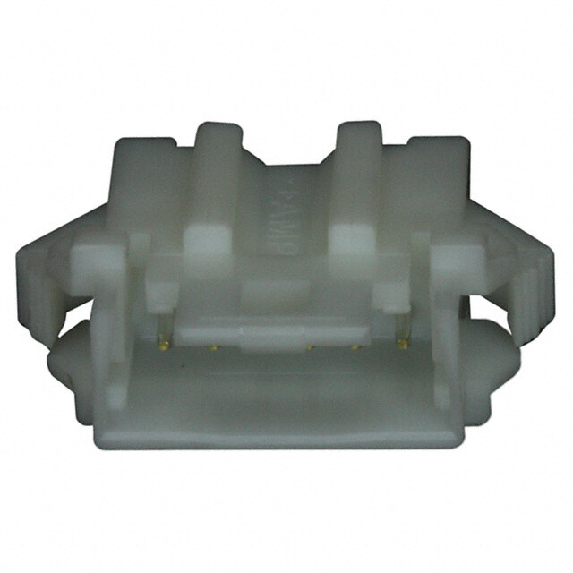
| 产品图片 |
|
| rohs | 符合RoHS无铅 / 符合限制有害物质指令(RoHS)规范要求 |
| 产品系列 | 放大器 IC,运算放大器 - 运放,Microchip Technology MCP651T-E/MNYmCal 技术 |
| 数据手册 | http://www.microchip.com/mymicrochip/filehandler.aspx?ddocname=en540974 |
| 产品型号 | MCP651T-E/MNY |
| PCN设计/规格 | http://www.microchip.com/mymicrochip/NotificationDetails.aspx?pcn=SYST-12DTLZ656&print=view |
| 产品种类 | 运算放大器 - 运放 |
| 供应商器件封装 | 8-TDFN(2x3) |
| 共模抑制比—最小值 | 65 dB |
| 关闭 | No Shutdown |
| 其它名称 | MCP651T-E/MNYDKR |
| 包装 | Digi-Reel® |
| 压摆率 | 30 V/µs |
| 商标 | Microchip Technology |
| 增益带宽生成 | 50 MHz |
| 增益带宽积 | 50MHz |
| 安装类型 | 表面贴装 |
| 安装风格 | SMD/SMT |
| 封装 | Reel |
| 封装/外壳 | 8-WFDFN 裸露焊盘 |
| 封装/箱体 | TDFN-8 |
| 工作温度 | -40°C ~ 125°C |
| 工作电源电压 | 2.2 V to 5.5 V |
| 工厂包装数量 | 3300 |
| 放大器类型 | 通用 |
| 最大工作温度 | + 125 C |
| 最小工作温度 | - 40 C |
| 标准包装 | 1 |
| 电压-电源,单/双 (±) | 2.5 V ~ 5.5 V |
| 电压-输入失调 | 200µV |
| 电流-电源 | 6mA |
| 电流-输入偏置 | 6pA |
| 电流-输出/通道 | 100mA |
| 电源电流 | 6 mA |
| 电路数 | 1 |
| 转换速度 | 30 V/us |
| 输入偏压电流—最大 | 6 nA |
| 输入补偿电压 | 200 uV |
| 输出电流 | 95 mA |
| 输出类型 | 满摆幅 |
| 通道数量 | 1 Channel |


PDF Datasheet 数据手册内容提取
MCP651/1S/2/3/4/5/9 50 MHz, 200 µV Op Amps with mCal Features: Description: • Gain-Bandwidth Product: 50MHz The Microchip Technology Inc. MCP651/1S/2/3/4/5/9 • Slew Rate: 30V/µs family of high bandwidth and high slew rate operational amplifiers features low offset. At power-up, these op • Low Input Offset: ±200µV (maximum) amps are self-calibrated using mCal. Some package • Low Input Bias Current: 6pA (typical) options also provide a Calibration/Chip Select pin • Noise: 7.5nV/Hz, at 1MHz (CAL/CS) that supports a Low-Power mode of • Ease-of-Use: operation, with offset calibration at the time normal - Unity-Gain Stable operation is re-started. These amplifiers are optimized - Rail-to-Rail Output for high speed, low noise and distortion, single-supply operation with rail-to-rail output and an input that - Input Range incl. Negative Rail includes the negative rail. - No Phase Reversal This family is offered in single (MCP651 and • Supply Voltage Range: +2.5V to +5.5V MCP651S), single with CAL/CS pin (MCP653), dual • High Output Current: ±100mA (MCP652), dual with CAL/CS pins (MCP655), quad • Supply Current: 6.0mA/Ch (typical) (MCP654) and quad with CAL/CS pins (MCP659). All • Low-Power Mode: 5µA/Ch devices are fully specified from -40°C to +125°C. • Small Packages: SOT23-5, DFN Typical Application Circuit • Extended Temperature Range: -40°C to +125°C MCP65X V Typical Applications: IN V OUT • Driving A/D Converters R L • Fast Low-side Current Sensing V /2 DD • Power Amplifier Control Loops 1k 100k • Optical Detector Amplifier High Gain Amplifier (G = 101V/V) • Barcode Scanners • Multi-Pole Active Filter 35% • Consumer Audio s 80 Samples ce30% TA = +25°C en VDD = 2.5V and 5.5V Design Aids: urr25% Calibrated at +25°C c c20% • SPICE Macro Models of O15% • FilterLab® Software e g a10% • Microchip Advanced Part Selector (MAPS) nt e • Analog Demonstration and Evaluation Boards erc 5% P - MCP651EV-VOS 0% -100 -80 -60 -40 -20 0 20 40 60 80 100 • Application Notes Input Offset Voltage (µV) High Gain-Bandwidth Op Amp Portfolio Model Family Channels/Package Gain-Bandwidth V (max.) I /Ch (typ.) OS Q MCP621/1S/2/3/4/5/9 1, 2, 4 20MHz 0.2mV 2.5mA MCP631/2/3/4/5/9 1, 2, 4 24MHz 8.0mV 2.5mA MCP651/1S/2/3/4/5/9 1, 2, 4 50MHz 0.2 mV 6.0mA MCP660/1/2/3/4/5/9 1, 2, 3, 4 60MHz 8.0 mV 6.0mA 2009-2014 Microchip Technology Inc. DS20002146D-page 1
MCP651/1S/2/3/4/5/9 Package Types MCP651 MCP651 MCP651S MCP654 SOIC 2x3TDFN* SOT-23-5 SOIC,TSSOP NC 1 8 CAL/CS NC 1 8 CAL/CS VOUT 1 5 VDD VOUTA 1 14 VOUTD VVIINN+– 23 76 VVDODUT VVIINN+– 23 E9P 76 VVDODUT VSS 2 VVININAA+- 23 1132 VVIINNDD-+ VSS 4 5 VCAL VSS 4 5 VCAL VIN+ 3 4 VIN– VDD 4 11 VSS VINB+ 5 10 VINC+ VINB- 6 9 VINC- VOUTB 7 8 VOUTC MCP652 MCP652 MCP653 3x3DFN* SOIC SOT-23-6 MCP659 VOUTA 1 8 VDD VOUTA 1 8 VDD VOUT 1 6 VDD 4x4QFN* VINA– 2 EP 7 VOUTB VINA– 2 7 VOUTB VINA+ 3 9 6 VINB– VINA+ 3 6 VINB– VSS 2 5 CAL/CS SAD VSS 4 5 VINB+ VSS 4 5 VINB+ VIN+ 3 4 VIN– UTA L/CAD UTD -D O A O N V C V VI 16 15 14 13 MCP655 MCP655 3x3DFN* MSOP VINA- 1 12 VIND+ VINA+ 2 EP 11 VSS VOUTA 1 10 VDD VOUTA 1 10VDD VDD 3 17 10 VINC+ VINA– 2 EP 9 VOUTB VINA– 2 9 VOUTB VINB+ 4 9 VINC- VINA+ 3 11 8 VINB– VINA+ 3 8 VINB– 5 6 7 8 CALA/CVSSSA 45 76 VCIANLBB+/CSB CALA/CVSSAS 45 76 VCIANLBB+/CSB V-INB OUTB CSBC OUTC V /C V B L A *Includes Exposed Thermal Pad (EP); see Table3-1. C DS20002146D-page 2 2009-2014 Microchip Technology Inc.
MCP651/1S/2/3/4/5/9 1.0 ELECTRICAL CHARACTERISTICS 1.1 Absolute Maximum Ratings † †Notice: Stresses above those listed under “Absolute Maximum Ratings” may cause permanent damage to the VDD–VSS .......................................................................6.5V device. This is a stress rating only and functional operation of Current at Input Pins ....................................................±2mA the device at those or any other conditions above those Analog Inputs (V + and V –)†† .V –1.0V to V +1.0V indicated in the operational listings of this specification is not IN IN SS DD implied. Exposure to maximum rating conditions for extended All other Inputs and Outputs ..........V –0.3V to V +0.3V SS DD periods may affect device reliability. Difference Input voltage ......................................|V –V | DD SS Output Short Circuit Current ................................Continuous ††See Section4.2.2 “Input Voltage and Current Limits”. Current at Output and Supply Pins ..........................±150mA Storage Temperature ...................................-65°C to +150°C Max. Junction Temperature ........................................+150°C ESD protection on all pins (HBM, MM) 1kV,200V 1.2 Specifications TABLE 1-1: DC ELECTRICAL SPECIFICATIONS Electrical Characteristics: Unless otherwise indicated, T = +25°C, V = +2.5V to +5.5V, V = GND, V = V /3, A DD SS CM DD V V /2, V = V /2, R = 1k to V and CAL/CS=V (refer to Figure1-2). OUT DD L DD L L SS Parameters Sym. Min. Typ. Max. Units Conditions Input Offset Input Offset Voltage V -200 — +200 µV After calibration (Note1) OS Input Offset Voltage Trim Step V — 37 200 µV OSTRM Input Offset Voltage Drift V /T — ±2.5 — µV/°C T = -40°C to +125°C OS A A Power Supply Rejection Ratio PSRR 61 76 — dB Input Current and Impedance Input Bias Current I — 6 — pA B Across Temperature I — 130 — pA T = +85°C B A Across Temperature I — 1700 5,000 pA T = +125°C B A Input Offset Current I — ±1 — pA OS Common Mode Input Impedance Z — 1013||9 — ||pF CM Differential Input Impedance Z — 1013||2 — ||pF DIFF Common Mode Common Mode Input Voltage Range V V 0.3 — V 1.3 V (Note2) CMR SS DD Common Mode Rejection Ratio CMRR 65 81 — dB V = 2.5V, V = -0.3 to 1.2V DD CM CMRR 68 84 — dB V = 5.5V, V = -0.3 to 4.2V DD CM Open-Loop Gain DC Open-Loop Gain (large signal) A 88 114 — dB V = 2.5V, V = 0.3V to 2.2V OL DD OUT A 94 123 — dB V = 5.5V, V = 0.3V to 5.2V OL DD OUT Output Maximum Output Voltage Swing V , V V +25 — V 25 mV V = 2.5V, G = +2, OL OH SS DD DD 0.5V Input Overdrive V , V V +50 — V 50 mV V = 5.5V, G = +2, OL OH SS DD DD 0.5V Input Overdrive Output Short-Circuit Current I ±50 ±95 ±145 mA V = 2.5V (Note3) SC DD I ±50 ±100 ±150 mA V = 5.5V (Note3) SC DD Note 1: Describes the offset (under the specified conditions) right after power-up, or just after the CAL/CS pin is toggled. Thus, 1/f noise effects (an apparent wander in V ; see Figure2-35) are not included. OS 2: See Figure2-6 and Figure2-7 for temperature effects. 3: The I specifications are for design guidance only; they are not tested. SC 2009-2014 Microchip Technology Inc. DS20002146D-page 3
MCP651/1S/2/3/4/5/9 TABLE 1-1: DC ELECTRICAL SPECIFICATIONS (CONTINUED) Electrical Characteristics: Unless otherwise indicated, T = +25°C, V = +2.5V to +5.5V, V = GND, V = V /3, A DD SS CM DD V V /2, V = V /2, R = 1k to V and CAL/CS=V (refer to Figure1-2). OUT DD L DD L L SS Parameters Sym. Min. Typ. Max. Units Conditions Calibration Input Calibration Input Voltage Range V V +0.1 — V –1.4 mV V pin externally driven CALRNG SS DD CAL Internal Calibration Voltage V 0.31V 0.33V 0.35V V pin open CAL DD DD DD CAL Input Impedance Z — 100||5 — k||pF CAL Power Supply Supply Voltage V 2.5 — 5.5 V DD Quiescent Current per Amplifier I 3 6 9 mA I = 0 Q O POR Input Threshold, Low VPRL 1.15 1.40 — V POR Input Threshold, High VPRH — 1.40 1.65 V Note 1: Describes the offset (under the specified conditions) right after power-up, or just after the CAL/CS pin is toggled. Thus, 1/f noise effects (an apparent wander in V ; see Figure2-35) are not included. OS 2: See Figure2-6 and Figure2-7 for temperature effects. 3: The I specifications are for design guidance only; they are not tested. SC TABLE 1-2: AC ELECTRICAL SPECIFICATIONS Electrical Characteristics: Unless otherwise indicated, T = 25°C, V = +2.5V to +5.5V, V = GND, V = V /2, A DD SS CM DD V V /2, V = V /2, R = 1k to V , C =20pF and CAL/CS=V (refer to Figure1-2). OUT DD L DD L L L SS Parameters Sym. Min. Typ. Max. Units Conditions AC Response Gain-Bandwidth Product GBWP — 50 — MHz Phase Margin PM — 65 — ° G = +1 Open-Loop Output Impedance R — 20 — OUT AC Distortion Total Harmonic Distortion plus Noise THD+N — 0.0012 — % G = +1, V = 4V , f = 1kHz, OUT P-P V = 5.5V, BW = 80kHz DD Step Response Rise Time, 10% to 90% t — 6 — ns G = +1, V = 100mV r OUT P-P Slew Rate SR — 30 — V/µs G = +1 Noise Input Noise Voltage E — 17 — µV f = 0.1Hz to 10Hz ni P-P Input Noise Voltage Density e — 7.5 — nV/Hz f = 1MHz ni Input Noise Current Density i 4 — fA/Hz f = 1kHz ni DS20002146D-page 4 2009-2014 Microchip Technology Inc.
MCP651/1S/2/3/4/5/9 TABLE 1-3: DIGITAL ELECTRICAL SPECIFICATIONS Electrical Characteristics: Unless otherwise indicated, T = 25°C, V = +2.5V to +5.5V, V = GND, V = V /2, A DD SS CM DD V V /2, V = V /2, R = 1k to V , C =20pF and CAL/CS=V (refer to Figure1-1 and Figure1-2). OUT DD L DD L L L SS Parameters Sym. Min. Typ. Max. Units Conditions CAL/CS Low Specifications CAL/CS Logic Threshold, Low V V — 0.2V V IL SS DD CAL/CS Input Current, Low I — 0 — nA CAL/CS = 0V CSL CAL/CS High Specifications CAL/CS Logic Threshold, High V 0.8V V V IH DD DD CAL/CS Input Current, High I — 0.7 — µA CAL/CS = V CSH DD GND Current I -3.5 -1.8 — µA Single, CAL/CS = V = 2.5V SS DD I -8 -4 — µA Single, CAL/CS = V = 5.5V SS DD I -5 -2.5 — µA Dual, CAL/CS = V = 2.5V SS DD I -10 -5 — µA Dual, CAL/CS = V = 5.5V SS DD CAL/CS Internal Pull-Down Resistor R — 5 — M PD Amplifier Output Leakage I — 50 — nA CAL/CS = V O(LEAK) DD POR Dynamic Specifications V Low to Amplifier Off Time t — 200 — ns G = +1V/V, V = V , DD POFF L SS (output goes High Z) V =2.5V to 0V step to V =0.1 (2.5V) DD OUT V High to Amplifier On Time t 100 200 300 ms G = +1V/V, V = V , DD PON L SS (including calibration) V =0V to 2.5V step to V =0.9 (2.5V) DD OUT CAL/CS Dynamic Specifications CAL/CS Input Hysteresis V — 0.25 — V HYST CAL/CS Setup Time t 1 — — µs G = +1V/V, V = V (Notes2,3,4) CSU L SS (between CAL/CS edges) CAL/CS = 0.8V to V = 0.1 (V /2) DD OUT DD CAL/CS High to Amplifier Off Time t — 200 — ns G = +1V/V, V = V , COFF L SS (output goes High Z) CAL/CS = 0.8V to V = 0.1 (V /2) DD OUT DD CAL/CS Low to Amplifier On Time tCON — 3 4 ms G = +1V/V, VL = VSS, MCP651 and MCP655, (including calibration) CAL/CS = 0.2V to V = 0.9 (V /2) DD OUT DD tCON — 6 8 ms G = +1V/V, VL = VSS, MCP659, CAL/CS = 0.2V to V = 0.9 (V /2) DD OUT DD Note 1: The MCP652 single, MCP653 single, MCP655 dual and MCP659 quad have their CAL/CS inputs internally pulled down to V (0V). SS 2: This time ensures that the internal logic recognizes the edge. However, for the rising edge case, if CAL/CS is raised before the calibration is complete, the calibration will be aborted and the part will return to Low-Power mode. 3: For the MCP655 dual, there is an additional constraint. CALA/CSA and CALB/CSB can be toggled simultaneously (within a time much smaller than t ) to make both op amps perform the same function simultaneously. If they are tog- CSU gled independently, then CALA/CSA (CALB/CSB) cannot be allowed to toggle while op amp B (op amp A) is in Calibration mode; allow more than the maximum t time (4ms) before the other side is toggled. CON 4: For the MCP659 quad, there is an additional constraint. CALAD/CSAD and CALBC/CSBC can be toggled simultane- ously (within a time much smaller than t ) to make all four op amps perform the same function simultaneously, and CSU the maximum t time is approximately doubled (8 ms). If they are toggled independently, then CALAD/CSAD CON (CALBC/CSBC) cannot be allowed to toggle while op amps B and C (op amps A and D) are in Calibration mode; allow more than the maximum t time (8ms) before the other side is toggled. CON 2009-2014 Microchip Technology Inc. DS20002146D-page 5
MCP651/1S/2/3/4/5/9 TABLE 1-4: TEMPERATURE SPECIFICATIONS Electrical Characteristics: Unless otherwise indicated, all limits are specified for: V = +2.5V to +5.5V, V = GND. DD SS Parameters Sym. Min. Typ. Max. Units Conditions Temperature Ranges Specified Temperature Range T -40 — +125 °C A Operating Temperature Range T -40 — +125 °C (Note1) A Storage Temperature Range T -65 — +150 °C A Thermal Package Resistances Thermal Resistance, 5L-2×3SOT — 220.7 — °C/W JA Thermal Resistance, 6L-2×3SOT — 190.5 — °C/W JA Thermal Resistance, 8L-2×3TDFN — 52.5 — °C/W JA Thermal Resistance, 8L-3×3DFN — 63 — °C/W (Note2) JA Thermal Resistance, 8L-SOIC — 163 — °C/W JA Thermal Resistance, 10L-3×3DFN — 71 — °C/W (Note2) JA Thermal Resistance, 10L-MSOP — 202 — °C/W JA Thermal Resistance, 14L-SOIC — 95.3 — °C/W JA Thermal Resistance, 14L-TSSOP — 100 — °C/W JA Thermal Resistance, 16L-4x4-QFN — 46 — °C/W (Note2) JA Note 1: Operation must not cause T to exceed Maximum Junction Temperature specification (150°C). J 2: Measured on a standard JC51-7, four-layer printed circuit board with ground plane and vias. 1.3 Timing Diagram CAL/CS V V IH IL VDD VPRH t VPRL CSU t t t t PON COFF CON POFF VOUT High Z On High Z On High Z -6mA(typical) -6mA(typical) I -3µA(typical) -3µA(typical) -3µA(typical) SS ICS 0nA(typical) 0.7µA(typical) 0nA(typical) Note: For the MCP655 dual and the MCP659 quad, there is an additional constraint on toggling the two CAL/CS pins close together; see the T specification in Table1-3. CON FIGURE 1-1: Timing Diagram. DS20002146D-page 6 2009-2014 Microchip Technology Inc.
MCP651/1S/2/3/4/5/9 1.4 Test Circuits C F The circuit used for most DC and AC tests is shown in 6.8pF Figure1-2. This circuit can independently set V and CM V ; see Equation1-1. Note that V is not the OUT CM R R circuit’s Common mode voltage ((V +V )/2), and that G F P M 10k 10k V includes V plus the effects (on the input offset OST OS V V /2 error, V ) of temperature, CMRR, PSRR and A . P DD OST OL V DD V EQUATION 1-1: IN+ C C B1 B2 G = R R DM F G MCP65X 100nF 2.2µF V = V +V 22 CM P DD VOST = VIN––VIN+ VIN– V = V 2+V –V +V 1+G OUT DD P M OST DM VM VOUT Where: RG RF RL CL G = Differential Mode Gain (V/V) 10k 10k 1k 20pF DM V = Op Amp’s Common Mode (V) CM Input Voltage CF V 6.8pF L V = Op Amp’s Total Input Offset (mV) OST Voltage FIGURE 1-2: AC and DC Test Circuit for Most Specifications. 2009-2014 Microchip Technology Inc. DS20002146D-page 7
MCP651/1S/2/3/4/5/9 2.0 TYPICAL PERFORMANCE CURVES Note: The graphs and tables provided following this note are a statistical summary based on a limited number of samples and are provided for informational purposes only. The performance characteristics listed herein are not tested or guaranteed. In some graphs or tables, the data presented may be outside the specified operating range (e.g., outside specified power supply range) and therefore outside the warranted range. Note: Unless otherwise indicated, T =+25°C, V =+2.5V to 5.5V, V =GND, V =V /3, V =V /2, A DD SS CM DD OUT DD V =V /2, R =1kto V , C =20pF, and CAL/CS=V . L DD L L L SS 2.1 DC Signal Inputs 35% 700 s 80 Samples Representative Part ce30% TA = +25°C V) 600 Calibrated at VDD = 6.5V e of Occurren122505%%% VCDaDli b=r a2t.e5dV aatn +d2 55.°5CV set Voltage (µ 234500000000 ++12855°°CC ag10% Off +25°C ent ut 100 -40°C Perc 5% Inp 0 0% -100 -100 -80 -60 -40 -20 0 20 40 60 80 100 1.5 2.0 2.5 3.0 3.5 4.0 4.5 5.0 5.5 6.0 6.5 Input Offset Voltage (µV) Power Supply Voltage (V) FIGURE 2-1: Input Offset Voltage. FIGURE 2-4: Input Offset Voltage vs. Power Supply Voltage. 20% 50 ces18% 8V0D DS =a m2.p5lVes and 5.5V V) 40 Representative Part urren1146%% TCAa l=ib -r4a0te°dC atot ++2152°5C°C ge (µ 2300 VDD = 2.5V Occ12% olta 10 entage of 10468%%%% ut Offset V---3210000 VDD = 5.5V Perc 2% Inp-40 0% -50 -10 -8 -6 -4 -2 0 2 4 6 8 10 0.0 0.5 1.0 1.5 2.0 2.5 3.0 3.5 4.0 4.5 5.0 5.5 Input Offset Voltage Drift (µV/°C) Output Voltage (V) FIGURE 2-2: Input Offset Voltage Drift. FIGURE 2-5: Input Offset Voltage vs. Output Voltage. 55% 0.0 s50% 80 Samples 1 Lot centage of Occurrence1122334405050505%%%%%%%% TVAD D= = + 22.55°VC and 5C.C5ahVliabnragteiodn CCahN(liiabnoncr aClgutehidodaennsg neoise) Low Input CommonMode Headroom (V)----0000....4321 Low (VCMR_L – VSS) VDD = 2.5V VDD = 5.5V er 5% P 0% -0.5 -100 -80 -60 -40 -20 0 20 40 60 80 100 -50 -25 0 25 50 75 100 125 Input Offset Voltage Repeatability (µV) Ambient Temperature (°C) FIGURE 2-3: Input Offset Voltage FIGURE 2-6: Low-Input Common Mode Repeatability (repeated calibration). Voltage Headroom vs. Ambient Temperature. DS20002146D-page 8 2009-2014 Microchip Technology Inc.
MCP651/1S/2/3/4/5/9 Note: Unless otherwise indicated, T =+25°C, V =+2.5V to 5.5V, V =GND, V =V /3, V =V /2, A DD SS CM DD OUT DD V =V /2, R =1kto V , C =20pF, and CAL/CS=V . L DD L L L SS 1.4 110 1 Lot High (VDD – VCMR_H) 105 monm (V)1.3 dB) 10905 PSRR nput ComHeadroo1.2 VDD = 2.5V R, PSRR ( 889050 CMRR, VDD = 5.5V High IMode 1.1 VDD = 5.5V CMR 7705 CMRR, VDD = 2.5V 65 1.0 60 -50 -25 0 25 50 75 100 125 -50 -25 0 25 50 75 100 125 Ambient Temperature (°C) Ambient Temperature (°C) FIGURE 2-7: High-Input Common Mode FIGURE 2-10: CMRR and PSRR vs. Voltage Headroom vs. Ambient Temperature. Ambient Temperature. 1000 130 V) 800 VRDeDp r=e s2e.5nVtative Part B)125 VDD = 5.5V age (µ 460000 ain (d120 ut Offset Volt ---6422000000000 +-4205°°CC Open-Loop G111011505 VDD = 2.5V Inp -800 ++12855°°CC DC 100 -1000 95 6 4 2 0 2 4 6 8 0 2 4 6 8 0 0. 0. 0. 0. 0. 0. 0. 0. 1. 1. 1. 1. 1. 2. -50 -25 0 25 50 75 100 125 - - - Input Common Mode Voltage (V) Ambient Temperature (°C) FIGURE 2-8: Input Offset Voltage vs. FIGURE 2-11: DC Open-Loop Gain vs. Common Mode Voltage with V =2.5V. Ambient Temperature. DD 1000 10,000 ge (µV) 468000000 VRDeDp r=e s5e.5nVtative Part urrents 1,000 VVDCDM == 5V.C5MVR_H a C Offset Volt --2420000000 -40°C as, Offset (pA) 100 IB Input --860000 +++1282555°°°CCC nput Bi 10 -IOS -1000 I 1 5 0 5 0 5 0 5 0 5 0 5 0 0. 0. 0. 1. 1. 2. 2. 3. 3. 4. 4. 5. 25 45 65 85 105 125 - Input Common Mode Voltage (V) Ambient Temperature (°C) FIGURE 2-9: Input Offset Voltage vs. FIGURE 2-12: Input Bias and Offset Common Mode Voltage with V =5.5V. Currents vs. Ambient Temperature with DD V =+5.5V. DD 2009-2014 Microchip Technology Inc. DS20002146D-page 9
MCP651/1S/2/3/4/5/9 Note: Unless otherwise indicated, T =+25°C, V =+2.5V to 5.5V, V =GND, V =V /3, V =V /2, A DD SS CM DD OUT DD V =V /2, R =1kto V , C =20pF, and CAL/CS=V . L DD L L L SS 160 1.E-10m3 Input Bias, Offset Currents(pA)111---246802464200000000000 TVAD D= = + 58.55°VC IIOBS Input Current Magnitude (A)111111111.........11EEEEEEEEE1110001---------111000000000011100210987654nnppnpµµµ +++1-28245550°°°°CCCC 0.0 0.5 1.0 1.5 2.0 2.5 3.0 3.5 4.0 4.5 5.0 5.5 -1.0 -0.9 -0.8 -0.7 -0.6 -0.5 -0.4 -0.3 -0.2 -0.1 0.0 Common Mode Input Voltage (V) Input Voltage (V) FIGURE 2-13: Input Bias and Offset FIGURE 2-15: Input Bias Current vs. Input Currents vs. Common Mode Input Voltage with Voltage (below V ). SS T =+85°C. A 2000 s TA = +125°C nt 1500 VDD = 5.5V urre IB C 1000 Offset (pA) 500 Bias, 0 IOS ut -500 p n I -1000 0.0 0.5 1.0 1.5 2.0 2.5 3.0 3.5 4.0 4.5 5.0 5.5 Common Mode Input Voltage (V) FIGURE 2-14: Input Bias and Offset Currents vs. Common Mode Input Voltage with T =+125°C. A DS20002146D-page 10 2009-2014 Microchip Technology Inc.
MCP651/1S/2/3/4/5/9 Note: Unless otherwise indicated, T =+25°C, V =+2.5V to 5.5V, V =GND, V =V /3, V =V /2, A DD SS CM DD OUT DD V =V /2, R =1kto V , C =20pF, and CAL/CS=V . L DD L L L SS 2.2 Other DC Voltages and Currents 14 8 m toA)12 VDD = 5.5V VOL – VSS 7 of Output Headrooput Current (mV/m10468 VDD = 2.5V VD-DII OO–UU TTVOH Supply Current(mA/amplifier)23456 +++1-28245550°°°°CCCC atio Out 2 1 R 0 0 1 10 100 0.0 0.5 1.0 1.5 2.0 2.5 3.0 3.5 4.0 4.5 5.0 5.5 6.0 6.5 Output Current Magnitude (mA) Power Supply Voltage (V) FIGURE 2-16: Ratio of Output Voltage FIGURE 2-19: Supply Current vs. Power Headroom to Output Current. Supply Voltage. 14 9 RL = 1 kΩ VOL – VSS 8 V)12 m (m10 VDD = 5.5V enter)67 VDD = 5.5V Output Headroo 2468 VDD = 2.5V VDD – VOH Supply Curr(mA/amplifi12345 VDD= 2.5V 0 0 0 5 0 5 0 5 0 5 0 5 0 5 -50 -25 0 25 50 75 100 125 0. 0. 1. 1. 2. 2. 3. 3. 4. 4. 5. 5. Ambient Temperature (°C) Common Mode Input Voltage (V) FIGURE 2-17: Output Voltage Headroom FIGURE 2-20: Supply Current vs. Common vs. Ambient Temperature. Mode Input Voltage. 100 1.8 ent 80 1.6 ut Short Circuit Curr(mA) ---6422460000000 +++-41820255°5°°CCC°C OR Trip Voltages (V)000111......468024 VVPPRRLH utp -80 P0.2 O -100 0.0 0.0 0.5 1.0 1.5 2.0 2.5 3.0 3.5 4.0 4.5 5.0 5.5 6.0 6.5 -50 -25 0 25 50 75 100 125 Power Supply Voltage (V) Ambient Temperature (°C) FIGURE 2-18: Output Short-Circuit Current FIGURE 2-21: Power-On Reset Voltages vs. Power Supply Voltage. vs. Ambient Temperature. 2009-2014 Microchip Technology Inc. DS20002146D-page 11
MCP651/1S/2/3/4/5/9 Note: Unless otherwise indicated, T =+25°C, V =+2.5V to 5.5V, V =GND, V =V /3, V =V /2, A DD SS CM DD OUT DD V =V /2, R =1kto V , C =20pF, and CAL/CS=V . L DD L L L SS s30% 140 ce 144 Samples Ω) Occurren122505%%% VDD = 2.5V and 5.5V stance (k 110200 age of 105%% ResiAL 6800 Percent 0% 33.20% 33.24% 33.28% 33.32% 33.36% 33.40% 33.44% 33.48% 33.52% Internal VC 24000 Normalized Internal Calibration Voltage; -50 -25 0 25 50 75 100 125 VCAL/VDD Ambient Temperature (°C) FIGURE 2-22: Normalized Internal FIGURE 2-23: V Input Resistance vs. CAL Calibration Voltage. Temperature. DS20002146D-page 12 2009-2014 Microchip Technology Inc.
MCP651/1S/2/3/4/5/9 Note: Unless otherwise indicated, T =+25°C, V =+2.5V to 5.5V, V =GND, V =V /3, V =V /2, A DD SS CM DD OUT DD V =V /2, R =1kto V , C =20pF, and CAL/CS=V . L DD L L L SS 2.3 Frequency Response 90 90 70 PM 80 PSRR+ uct 80 60 RR, PSRR (dB)3456700000 CMRR PSRR- Bandwidth Prod(MHz)567000 VDGDB=W 2P.5V VDD = 5.5V 345000 hase Margin (°) CM20 ain 40 20 P G 10 30 10 0 5 0 5 0 5 0 5 0 5 0 5 0 5 0 11.E0+02 1.1Ek+3 11.E0+k4 110.E0+k5 11.EM+6 11.0EM+7 0. 0. 0. 1. 1. 2. 2. 3. 3. 4. 4. 5. 5. 6. Frequency (Hz) - Common Mode Input Voltage (V) FIGURE 2-24: CMRR and PSRR vs. FIGURE 2-27: Gain-Bandwidth Product Frequency. and Phase Margin vs. Common Mode Input Voltage. 120 0 60 90 Open-Loop Gain (dB)10246800000 | AOL | AOL -----119635200000 Open-Loop Phase (°) ain Bandwidth Product(MHz)1234500000 GBPWMP VDD =V 2DD.5 =V 5.5V 4567800000 Phase Margin (°) 0 -180 G 0 30 -20 -210 1.1E0+1 11.E0+02 1.1Ek+3 11.E0+k4110.E0+k5 11.EM+6 11.0EM+7110.E0+M8 11.EG+9 0.00.51.01.52.02.53.03.54.04.55.05.5 Frequency (Hz) Output Voltage (V) FIGURE 2-25: Open-Loop Gain vs. FIGURE 2-28: Gain-Bandwidth Product Frequency. and Phase Margin vs. Output Voltage. 90 70 Ω)1000 uct 80 PM 60 ance ( dwidth Prod(MHz)6700 GBWP VVDDDD == 52..55VV 4500 e Margin (°) utput Imped 11000 GG =G = 1= 01 111 VVV///VVV Ban 50 30 has p O n P oo 1 Gai 40 20 n-L e 30 10 p O 0.1 -50 -25 0 25 50 75 100 125 1k 10k 100k 1M 10M 100M 1.0E+03 1.0E+04 1.0E+05 1.0E+06 1.0E+07 1.0E+08 Ambient Temperature (°C) Frequency (Hz) FIGURE 2-26: Gain-Bandwidth Product FIGURE 2-29: Closed-Loop Output and Phase Margin vs. Ambient Temperature. Impedance vs. Frequency. 2009-2014 Microchip Technology Inc. DS20002146D-page 13
MCP651/1S/2/3/4/5/9 Note: Unless otherwise indicated, T =+25°C, V =+2.5V to 5.5V, V =GND, V =V /3, V =V /2, A DD SS CM DD OUT DD V =V /2, R =1kto V , C =20pF, and CAL/CS=V . L DD L L L SS 10 150 9 140 RRSS == 01Ω kΩ Gain Peaking (dB) 2345678 GGG ==(cid:149) 412 VVV///VVV Channel-to-ChannelSeparation (dB)111101237890000000 RVGCT =MI +=1 V VDD/V/2 01 5600 RRSS= = 1 0100 kkΩΩ 1.01E0p-11 100p 1.0E-10 1n 1.01E0-n09 1.E1+k03 1.1E0+k04 11.E0+00k5 1.E1M+06 1.1E0+M07 Normalized Capacitive Load; C/G (F) Frequency (Hz) L FIGURE 2-30: Gain Peaking vs. FIGURE 2-31: Channel-to-Channel Normalized Capacitive Load. Separation vs. Frequency. DS20002146D-page 14 2009-2014 Microchip Technology Inc.
MCP651/1S/2/3/4/5/9 Note: Unless otherwise indicated, T =+25°C, V =+2.5V to 5.5V, V =GND, V =V /3, V =V /2, A DD SS CM DD OUT DD V =V /2, R =1kto V , C =20pF, and CAL/CS=V . L DD L L L SS 2.4 Input Noise and Distortion Hz)(cid:165)11.E0+µ4 20 Representative Part V/ 15 NPBW = 0.1 Hz Voltage Density (n1110..EE01++nµ23 ut Offset + Noise;V + e(t) (µV)OSni-11-00505 oise 11.E0+n1 Inp -15 N Input 1.E1+n010.E.1-1 1.E1+0 1.1E0+1 11F.E0r+e02qu1e.1Enk+c3y (11H.E0z+k)4 11.0E0+5k 11.EM+6 11.0E+M7 -20 0 5 10 15 2T0ime2 5(min3)0 35 40 45 50 FIGURE 2-32: Input Noise Voltage Density FIGURE 2-35: Input Noise plus Offset vs. vs. Frequency. Time with 0.1Hz Filter. 160 1 sity 140 VDD = 2.5V VDD = 5.0V n oltage DeHz)11802000 VDD = 5.5V oise (%) 00.0.11 BW = 22 Hz to > 500 kHz GG == 11 1V V/V/V VV/ N e n 60 + ois( 40 HD N T 0.001 ut 20 BW = 22 Hz to 80 kHz p f = 100 Hz In 0 5 0 5 0 5 0 5 0 5 0 5 0 5 0 0.0001 0. 0. 0. 1. 1. 2. 2. 3. 3. 4. 4. 5. 5. 6. 11.E0+02 1.1Ek+3 11.E0+k4 11.0E0+5k - Common Mode Input Voltage (V) Frequency (Hz) FIGURE 2-33: Input Noise Voltage Density FIGURE 2-36: THD+N vs. Frequency. vs. Input Common Mode Voltage with f=100Hz. 12 nsity 1101 VDD = 2.5V De 9 e 8 VoltagV/Hz)(cid:165) 67 VDD = 5.5V e n 5 ois( 4 N 3 ut 2 p n 1 f = 1 MHz I 0 5 0 5 0 5 0 5 0 5 0 5 0 5 0. 0. 0. 1. 1. 2. 2. 3. 3. 4. 4. 5. 5. - Common Mode Input Voltage (V) FIGURE 2-34: Input Noise Voltage Density vs. Input Common Mode Voltage with f=1MHz. 2009-2014 Microchip Technology Inc. DS20002146D-page 15
MCP651/1S/2/3/4/5/9 Note: Unless otherwise indicated, T =+25°C, V =+2.5V to 5.5V, V =GND, V =V /3, V =V /2, A DD SS CM DD OUT DD V =V /2, R =1kto V , C =20pF, and CAL/CS=V . L DD L L L SS 2.5 Time Response 5.5 age (10 mV/div) VIN VOUT VGD =D =1 5.5V Voltage (V)233445......505050 VGRDF =D = V=- 14I N59.95ΩV olt ut 2.0 V p utput Out11..05 VOUT O 0.5 0.0 0 20 40 60 80 100 120 140 160 180 200 0 100 200 300 400 500 600 700 800 Time (ns) Time (ns) FIGURE 2-37: Non-inverting Small Signal FIGURE 2-40: Inverting Large Signal Step Step Response. Response. 5.5 7 5.0 VGD =D =1 5.5V V) 6 VIN VGD =D =2 5.5V Voltage (V)23344.....50505 ut Voltages ( 345 VOUT put 2.0 VIN VOUT utp 2 Out11..05 ut, O 1 p 0 0.5 In 0.0 -1 0 100 200 300 400 500 600 700 800 0 1 2 3 4 5 6 7 8 9 10 Time (ns) Time (ms) FIGURE 2-38: Non-inverting Large Signal FIGURE 2-41: The MCP651/1S/2/3/4/5/9 Step Response. family shows no input phase reversal with overdrive. V/div) VIN 5650 Falling Edge VDD = 5.5V m 50 utput Voltage (10 VGRDF = D= =- 14 59.95ΩV Slew Rate (V/µs)12233445050505 Rising Edge VDD = 2.5V O VOUT 10 5 0 50 100 150 200 250 300 350 400 0 Time (ns) -50 -25 0 25 50 75 100 125 Ambient Temperature (°C) FIGURE 2-39: Inverting Small Signal Step Response. FIGURE 2-42: Slew Rate vs. Ambient Temperature. DS20002146D-page 16 2009-2014 Microchip Technology Inc.
MCP651/1S/2/3/4/5/9 Note: Unless otherwise indicated, T =+25°C, V =+2.5V to 5.5V, V =GND, V =V /3, V =V /2, A DD SS CM DD OUT DD V =V /2, R =1kto V , C =20pF, and CAL/CS=V . L DD L L L SS 10 e ag VDD = 5.5V olt put VV)P-P VDD = 2.5V utg ( 1 On m wi uS m xi a M 0.1 100k 1M 10M 100M 1.E+05 1.E+06 1.E+07 1.E+08 Frequency (Hz) FIGURE 2-43: Maximum Output Voltage Swing vs. Frequency. 2009-2014 Microchip Technology Inc. DS20002146D-page 17
MCP651/1S/2/3/4/5/9 Note: Unless otherwise indicated, T =+25°C, V =+2.5V to 5.5V, V =GND, V =V /3, V =V /2, A DD SS CM DD OUT DD V =V /2, R =1kto V , C =20pF, and CAL/CS=V . L DD L L L SS 2.6 Calibration and Chip Select Response 1.1 0.40 1.0 CAL/CS = VDD 0.35 nt (µA)000...789 esis (V)00..2350 VDD = 5.5V urre0.6 ster0.20 CS C00..45 S Hy0.15 VDD = 2.5V AL/0.3 L/C0.10 C0.2 CA0.05 0.1 0.0 0.00 0.0 0.5 1.0 1.5 2.0 2.5 3.0 3.5 4.0 4.5 5.0 5.5 -50 -25 0 25 50 75 100 125 Power Supply Voltage (V) Ambient Temperature (°C) FIGURE 2-44: CAL/CS Current vs. Power FIGURE 2-47: CAL/CS Hysteresis vs. Supply Voltage. Ambient Temperature. AL/CS, V (V)OUT 0123456789 Otuprn As mofpf ICVDOADULT/CS VGVDL =D= =10 VCs2t.aa5lrVitbsration Otuprn As monp -----02468186420Power Supply Current;I (mA)DD CAL/CS Turn On Time (ms)01122334........50505050 C-1 -12 0.0 0 1 2 3 4 5 6 7 8 9 10 -50 -25 0 25 50 75 100 125 Time (ms) Ambient Temperature (°C) FIGURE 2-45: CAL/CS Voltage, Output FIGURE 2-48: CAL/CS Turn-On Time vs. Voltage and Supply Current (for Side A) vs. Time Ambient Temperature. with V =2.5V. DD AL/CS, V (V)OUT11012345678901 VGVOtuDL pr =Dn= A s =10 mo V5fp.f5VCAVLIOD/CDUTS Cstaalritbsration Otuprn As monp ------024681118642020Power Supply Current;I (mA)DD CAL/CS Pull-down Resistor(MΩ)12345678 Representative Part C -1 -14 0 0 1 2 3 4 5 6 7 8 9 10 -50 -25 0 25 50 75 100 125 Time (ms) Ambient Temperature (°C) FIGURE 2-46: CAL/CS Voltage, Output FIGURE 2-49: CAL/CS’s Pull-Down Voltage and Supply Current (for Side A) vs. Time Resistor (R ) vs. Ambient Temperature. PD with V =5.5V. DD DS20002146D-page 18 2009-2014 Microchip Technology Inc.
MCP651/1S/2/3/4/5/9 Note: Unless otherwise indicated, T =+25°C, V =+2.5V to 5.5V, V =GND, V =V /3, V =V /2, A DD SS CM DD OUT DD V =V /2, R =1kto V , C =20pF, and CAL/CS=V . L DD L L L SS 0 1.E-06 Negative Power SupplyCurrent; I (µA)SS------654321 +++1-28245550°°°°CCCC CAL/CS = VDD utput Leakage Current (A)1111....EEEE----10000987 CAL/CS = VDD = 5.5V ++18255°°CC O +25°C -7 1.E-11 0 5 0 5 0 5 0 5 0 5 0 5 0 5 0. 0. 1. 1. 2. 2. 3. 3. 4. 4. 5. 5. 6. 6. 0.00.51.01.52.02.53.0 3.54.04.55.05.56.0 Power Supply Voltage (V) Output Voltage (V) FIGURE 2-50: Quiescent Current in FIGURE 2-51: Output Leakage Current vs. Shutdown vs. Power Supply Voltage. Output Voltage. 2009-2014 Microchip Technology Inc. DS20002146D-page 19
MCP651/1S/2/3/4/5/9 3.0 PIN DESCRIPTIONS Descriptions of the pins are listed in Table3-1. TABLE 3-1: PIN FUNCTION TABLE MCP651 MCP651S MCP652 MCP653 MCP654 MCP655 MCP659 Symbol Description SOIC TDFN SOT SOIC DFN SOT SOIC TSSOP MSOP DFN QFN 6 6 1 1 1 1 1 1 1 1 16 V , Output (op amp A) OUT V OUTA 2 2 4 2 2 4 2 2 2 2 1 V –, V – Inverting Input (op IN INA amp A) 3 3 3 3 3 3 3 3 3 3 2 V +, V + Non-inverting Input IN INA (op amp A) 4 4 2 4 4 2 11 11 4 4 11 V Negative Power SS Supply 8 8 — — — 5 — — 5 5 — CAL/CS, Calibrate/Chip CALA/CSA Select Digital Input (op amp A) — — — — — — — — 6 6 — CALB/CSB Calibrate/Chip Select Digital Input (op amp B) — — — — — — — — — — 15 CALAD/ Calibrate/Chip CSAD Select Digital Input (op amps A and D) — — — — — — — — — — 7 CALBC/ Calibrate/Chip CSBC Select Digital Input (op amps B and C) — — — 5 5 — 5 5 7 7 4 V + Non-inverting Input INB (op amp B) — — — 6 6 — 6 6 8 8 5 V – Inverting Input (op INB amp B) — — — 7 7 — 7 7 9 9 6 V Output (op amp B) OUTB — — — — — — 10 10 — — 10 V + Non-inverting input INC (op amp C) — — — — — — 9 9 — — 9 V - Inverting Input (op INC amp C) — — — — — — 8 8 — — 8 V Output (op amp C) OUTC — — — — — — 12 12 — — 12 V + Non-inverting Input IND (op amp D) — — — — — — 13 13 — — 13 V - Inverting Input (op IND amp D) — — — — — — 14 14 — — 14 V Output (op amp D) OUTD 7 7 5 8 8 6 4 4 10 10 3 V Positive Power DD Supply 5 5 — — — — — — — — — V Calibration Com- CAL mon Mode Voltage Input 1 1 — — — — — — — — — NC No Internal Connection — 9 — — 9 — — — — 11 17 EP Exposed Thermal Pad (EP); must be connected to V SS DS20002146D-page 20 2009-2014 Microchip Technology Inc.
MCP651/1S/2/3/4/5/9 3.1 Analog Outputs 3.5 Calibrate/Chip Select Digital Input The analog output pins (V ) are low-impedance This input (CAL/CS, …) is a CMOS, Schmitt-Triggered OUT voltage sources. input that affects the Calibration and Low-Power modes of operation. When this pin goes high, the part 3.2 Analog Inputs is placed into a Low-Power mode and the output is High Z. When this pin goes low, a calibration sequence The non-inverting and inverting inputs (VIN+, VIN–, …) is started (which corrects VOS). At the end of the cali- are high-impedance CMOS inputs with low bias bration sequence, the output becomes low-impedance currents. and the part resumes normal operation. An internal POR triggers a calibration event when the 3.3 Power Supply Pins part is powered on, or when the supply voltage drops The positive power supply (V ) is 2.5V to 5.5V higher too low. Thus, the MCP652 parts are calibrated, even DD than the negative power supply (V ). For normal though they do not have a CAL/CS pin. SS operation, the other pins are between V and V . SS DD 3.6 Exposed Thermal Pad (EP) Typically, these parts are used in a single (positive) supply configuration. In this case, VSS is connected to There is an internal connection between the Exposed ground and VDD is connected to the supply. VDD will Thermal Pad (EP) and the VSS pin; they must be need bypass capacitors. connected to the same potential on the Printed Circuit Board (PCB). 3.4 Calibration Common Mode This pad can be connected to a PCB ground plane to Voltage Input provide a larger heat sink. This improves the package thermal resistance ( ). A low-impedance voltage placed at this input (V ) JA CAL will set the op amps’ Common mode input voltage during calibration. If this pin is left open, the Common mode input voltage during calibration is approximately V /3. The internal resistor divider is disconnected DD from the supplies whenever the part is not in calibra- tion. 2009-2014 Microchip Technology Inc. DS20002146D-page 21
MCP651/1S/2/3/4/5/9 4.0 APPLICATIONS For the MCP655 dual and the MCP659 quad, there is an additional constraint on toggling the two CAL/CS The MCP651/1S/2/3/4/5/9 family of self-zeroed op pins close together; see the t specification in CON amps is manufactured using Microchip’s state-of-the- Table1-3. If the two pins are toggled simultaneously, or art CMOS process. It is designed for low-cost, low- if they are toggled separately with an adequate delay power and high-precision applications. Its low supply between them (greater than t ), then the CAL/CS CON voltage, low quiescent current and wide bandwidth inputs are accepted as valid. If one of the two pins makes the MCP651/1S/2/3/4/5/9 ideal for battery- toggles while the other pin’s calibration routine is in powered applications. progress, then an invalid input occurs and the result is unpredictable. 4.1 Calibration and Chip Select 4.1.3 INTERNAL POR These op amps include circuitry for dynamic calibration This part includes an internal Power-On Reset (POR) of the offset voltage (V ). OS to protect the internal calibration memory cells. The 4.1.1 mCal CALIBRATION CIRCUITRY POR monitors the power supply voltage (VDD). When the POR detects a low V event, it places the part into DD The internal mCal circuitry, when activated, starts a the Low-Power mode of operation. When the POR delay timer (to wait for the op amp to settle to its new detects a normal V event, it starts a delay counter, DD bias point), then calibrates the input offset voltage then triggers an calibration event. The additional delay (V ). The mCal circuitry is triggered at power-up (and OS gives a total POR turn-on time of 200ms (typical); this after some power brown-out events) by the internal is also the power-up time (since the POR is triggered at POR, and by the memory’s Parity Detector. The power- power-up). up time, when the mCal circuitry triggers the calibration sequence, is 200ms (typical). 4.1.4 PARITY DETECTOR 4.1.2 CAL/CS PIN A parity error detector monitors the memory contents for any corruption. In the rare event that a parity error is The CAL/CS pin gives the user a means to externally detected (e.g., corruption from an alpha particle), a demand a Low-Power mode of operation, then to POR event is automatically triggered. This will cause calibrate V . Using the CAL/CS pin makes it possible OS the input offset voltage to be re-corrected, and the op to correct V as it drifts over time (1/f noise and aging; OS amp will not return to normal operation for a period of see Figure2-35) and across temperature. time (the POR turn-on time, t ). PON The CAL/CS pin performs two functions: it places the op amp(s) in a Low-Power mode when it is held high, 4.1.5 CALIBRATION INPUT PIN and starts a calibration event (correction of VOS) after a A VCAL pin is available in some options (e.g., the single rising edge. MCP651) for those applications that need the While in the Low-Power mode, the quiescent current is calibration to occur at an internally driven Common quite small (ISS=-3µA, typical). The output is also in a mode voltage other than VDD/3. High Z state. Figure4-1 shows the reference circuit that internally During the calibration event, the quiescent current is sets the op amp’s Common mode reference voltage near, but smaller than, the specified quiescent current (VCM_INT) during calibration (the resistors are (6mA, typical). The output continues in the High Z disconnected from the supplies at other times). The state, and the inputs are disconnected from the 5k resistor provides over-current protection for the external circuit, to prevent internal signals from buffer. affecting circuit operation. The op amp inputs are internally connected to a Common mode voltage buffer V Toopampduring and feedback resistors. The offset is corrected (using a DD calibration digital state machine, logic and memory), and the calibration constants are stored in memory. V 300k CM_INT 5k Once the calibration event is completed, the amplifier is reconnected to the external circuitry. The turn-on time, V CAL when calibration is started with the CAL/CS pin, is 3ms BUFFER (typical). 150k There is an internal 5M pull-down resistor tied to the CAL/CS pin. If the CAL/CS pin is left floating, the V SS amplifier operates normally. FIGURE 4-1: Common-Mode Reference’s Input Circuitry. DS20002146D-page 22 2009-2014 Microchip Technology Inc.
MCP651/1S/2/3/4/5/9 When the V pin is left open, the internal resistor above V ; their breakdown voltage is high enough to CAL DD divider generates a V of approximately V /3, allow normal operation, and low enough to bypass CM_INT DD which is near the center of the input Common mode quick ESD events within the specified limits. voltage range. It is recommended that an external capacitor from V to ground be added to improve CAL noise immunity. Bond V DD Pad When the V pin is driven by an external voltage CAL source, which is within its specified range, the op amp will have its input offset voltage calibrated at that Common mode input voltage. Make sure that V is Bond Input Bond CAL V + V – within its specified range. IN Pad Stage Pad IN It is possible to use an external resistor voltage divider to modify V ; see Figure4-2. The internal circuitry CM_INT at the V pin looks like 100k tied to V /3. The Bond CAL DD V SS parallel equivalent of R and R should be much Pad 1 2 smaller than 100k to minimize differences in matching and temperature drift between the internal FIGURE 4-3: Simplified Analog Input ESD and external resistors. Again, make sure that VCAL is Structures. within its specified range. In order to prevent damage and/or improper operation of these amplifiers, the circuit must limit the currents V DD (and voltages) at the input pins (see Section1.1 “Absolute Maximum Ratings†”). Figure4-4 shows MCP65X the recommended approach to protecting these inputs. R1 The internal ESD diodes prevent the input pins (VIN+ and V –) from going too far below ground, and the IN C VCAL resistors R1 and R2 limit the possible current drawn out 1 of the input pins. Diodes D and D prevent the input 1 2 R2 pins (VIN+ and VIN–) from going too far above VDD, and dump any currents onto V . When implemented as DD shown, resistors R and R also limit the current 1 2 VSS through D1 and D2. FIGURE 4-2: Setting V with External CM Resistors. VDD For instance, a design goal to set V =0.1V when CM_INT VDD=2.5V could be met with: R1=24.3k, D1 D2 R2=1.00k and C1=100nF. This will keep VCAL R1 MCP65X within its range for any VDD, and should be close V1 enough to 0V for ground-based applications. VOUT V 2 R 2 4.2 Input V –(minimum expected V ) SS 1 4.2.1 PHASE REVERSAL R1> 2mA The input devices are designed to not exhibit phase VSS–(minimum expected V2) R > inversion when the input pins exceed the supply 2 2mA voltages. Figure2-41 shows an input voltage FIGURE 4-4: Protecting the Analog exceeding both supplies with no phase inversion. Inputs. 4.2.2 INPUT VOLTAGE AND CURRENT It is also possible to connect the diodes to the left of the LIMITS resistor R and R . In this case, the currents through 1 2 The ESD protection on the inputs can be depicted as the diodes D and D need to be limited by some other 1 2 shown in Figure4-3. This structure was chosen to mechanism. The resistors then serve as in-rush current protect the input transistors, and to minimize input bias limiters; the DC current into the input pins (V + and IN current (I ). The input ESD diodes clamp the inputs V –) should be very small. B IN when they try to go more than one diode drop below V . They also clamp any voltages that go too far SS 2009-2014 Microchip Technology Inc. DS20002146D-page 23
MCP651/1S/2/3/4/5/9 A significant amount of current can flow out of the inputs (through the ESD diodes) when the Common 6.0 mFiogudree 2v-o1lt5a.g Aep p(lVicCaMti)o niss thbaet laorwe hgigrohu-inmdp e(dVaSnSc)e; mseaey 55..05 (VDD = 5.5V) VOH Limited 4.5 need to limit the usable voltage range. 4.0 RL = 1 kΩ RL = 100Ω 4T.h2e. 3input stNagOeR oMf tAheL MOCPPE6R5A1/T1ISO/2N/3/4/5/9 op amps V (V)OUT 12233.....50505 -I LimitedSC RL = 10Ω +I LimitedSC uses a differential PMOS input stage. It operates at low 1.0 0.5 Common mode input voltage (VCM), with VCM up to 0.0 VOL Limited V –1.3V and down to V –0.3V. The input offset -0.5 DD SS 0 0 0 0 0 0 0 0 0 0 0 0 0 vVoltag–e1 .(3VVO tSo) eisn smureea psruorpeedr aotp eVrCaMtio=n.V SSeSe– F0ig.3uVre a2n-6d -12 -10 -8 -6 -4 -2IOUT (mA2) 4 6 8 10 12 DD and Figure2-7 for temperature effects. FIGURE 4-6: Output Current. When operating at very low non-inverting gains, the output voltage is limited at the top by the V range CM (<V –1.3V); see Figure4-5. DD V DD MCP65X V IN V OUT V V V V –1.3V SS IN OUT DD FIGURE 4-5: Unity-Gain Voltage Limitations for Linear Operation. 4.3 Rail-to-Rail Output 4.3.0.1 Maximum Output Voltage The Maximum Output Voltage (see Figure2-16 and Figure2-17) describes the output range for a given load. For instance, the output voltage swings to within 15mV of the negative rail with a 1k load tied to V /2. DD 4.3.0.2 Output Current Figure4-6 shows the possible combinations of output voltage (V ) and output current (I ). I is OUT OUT OUT positive when it flows out of the op amp into the external circuit. DS20002146D-page 24 2009-2014 Microchip Technology Inc.
MCP651/1S/2/3/4/5/9 4.3.0.3 Power Dissipation Figure4-7 shows a capacitive load (C ), which is L driven by a sine wave with DC offset. The capacitive Since the output short circuit current (I ) is specified SC load causes the op amp to output higher currents at at ±100mA (typical), these op amps are capable of higher frequencies. Because the output rectifies I , both delivering and dissipating significant power. Two OUT the op amp’s dissipated power increases (even though common loads, and their impact on the op amp’s power the capacitor does not dissipate power). dissipation, will be discussed. Figure4-7 shows a resistive load (R ) with a DC output L voltage (VOUT). VL is RL’s ground point, VSS is usually VDD ground (0V) and I is the output current. The input OUT I currents are assumed to be negligible. DD I OUT MCP65X V OUT V DD C I L SS I DD I OUT V SS MCP65X VOUT FIGURE 4-8: Diagram for Capacitive Load I RL Power Calculations. SS V The output voltage is assumed to be: SS V L EQUATION 4-4: FIGURE 4-7: Diagram for Resistive Load V = V +V sint Power Calculations. OUT DC AC Where: The DC currents are: V = DC offset (V) DC EQUATION 4-1: VAC = Peak output swing (VPK) = Radian frequency (2f) (rad/s) V –V OUT L I = -------------------------- OUT R L The op amp’s currents are: I I +max0,I DD Q OUT I –I +min0,I SS Q OUT EQUATION 4-5: Where: dV I = Quiescent supply current for one I = C --------O---U----T-- = V C cost Q OUT L dt AC L op amp (mA/amplifier) I I +max0,I V = A DC value (V) DD Q OUT OUT I –I +min0,I SS Q OUT The DC op amp power is: Where: I = Quiescent supply current for one Q EQUATION 4-2: op amp (mA/amplifier) P = I V –V +I V –V OA DD DD OUT SS SS OUT The op amp’s instantaneous power, average power and peak power are: The maximum op amp power, for resistive loads at DC, occurs when V is halfway between V and V or OUT DD L halfway between V and V : EQUATION 4-6: SS L P = I V –V +I V –V OA DD DD OUT SS SS OUT EQUATION 4-3: 4V fC AC L aveP = V –V I +------------------------ maxPOA = IDDVDD–VSS OA DD SS Q 2 maxP = V –V I +2V fC max V –V V –V OA DD SS Q AC L +---------------------D---D--------------L---------L-------------S--S---- 4R L The power dissipated in a package depends on the powers dissipated by each op amp in that package: 2009-2014 Microchip Technology Inc. DS20002146D-page 25
MCP651/1S/2/3/4/5/9 EQUATION 4-7: When driving large capacitive loads with these op amps (e.g., >20pF when G=+1), a small series n resistor at the output (R in Figure4-9) improves the P = P ISO PKG OA feedback loop’s phase margin (stability) by making the k=1 output load resistive at higher frequencies. The Where: bandwidth will be generally lower than the bandwidth n = Number of op amps in package (1 or 2) with no capacitive load. The maximum ambient to junction temperature rise R R R G F ISO (T ) and junction temperature (T ) can be calculated JA J V OUT using the maximum expected package power (P ), PKG C ambient temperature (T ) and the package thermal L A resistance ( ) found in Table1-4: JA R MCP65X N EQUATION 4-8: FIGURE 4-9: Output Resistor, R ISO TJA = PPKGJA Stabilizes Large Capacitive Loads. T = T +T J A JA Figure4-10 gives recommended R values for ISO different capacitive loads and gains. The x-axis is the The worst-case power de-rating for the op amps in a normalized load capacitance (C /G ), where G is the L N N particular package can be easily calculated: circuit’s noise gain. For non-inverting gains, G and the N Signal Gain are equal. For inverting gains, G is N EQUATION 4-9: 1+|Signal Gain| (e.g., -1V/V gives G =+2V/V). N T –T P ----J--m----a---x------------A- PKG 100 JA Where: Ω) (O TJmax = Absolute maximum junction RIS temperature (°C) d de 10 T = Ambient temperature (°C) n A e m m GN = +1 Several techniques are available to reduce TJA for a Reco GN +2 given package: 1 • Reduce JA 1.1E0-p11 11.E00-1p0 1.E1n-09 1.1E0-n08 Normalized Capacitance; C/G (F) - Use another package L N - Improve the PCB layout (ground plane, etc.) FIGURE 4-10: Recommended R Values ISO - Add heat sinks and air flow for Capacitive Loads. • Reduce max(P ) PKG After selecting R for your circuit, double check the ISO - Increase R L resulting frequency response peaking and step - Decrease CL response overshoot. Modify RISO’s value until the - Limit I using R (see Figure4-9) response is reasonable. Bench evaluation and OUT ISO - Decrease V simulations with the MCP651/1S/2/3/4/5/9 SPICE DD macro model are helpful. 4.4 Improving Stability 4.4.2 GAIN PEAKING 4.4.1 CAPACITIVE LOADS Figure4-11 shows an op amp circuit that represents non-inverting amplifiers (V is a DC voltage and V is Driving large capacitive loads can cause stability M P the input) or inverting amplifiers (V is a DC voltage problems for voltage feedback op amps. As the load P and V is the input). The capacitances C and C capacitance increases, the feedback loop’s phase M N G represent the total capacitance at the input pins; they margin decreases and the closed-loop bandwidth is include the op amp’s Common mode input capacitance reduced. This produces gain peaking in the frequency (C ), board parasitic capacitance and any capacitor response, with overshoot and ringing in the step CM placed in parallel. response. See Figure2-30. A unity-gain buffer (G=+1) is the most sensitive to capacitive loads, though all gains show the same general behavior. DS20002146D-page 26 2009-2014 Microchip Technology Inc.
MCP651/1S/2/3/4/5/9 EQUATION 4-10: Given: C RN N MCP65X GN1 = 1+RFRG V P G = 1+C C V N2 G F OUT f = 12R C F F F VM fZ = fFGN1GN2 RG C RF We need: G f f 2G , G <G F GBWP N2 N1 N2 f f 4G , G >G FIGURE 4-11: Amplifier with Parasitic F GBWP N1 N1 N2 Capacitance. C acts in parallel with R (except for a gain of +1V/V), 4.5 Power Supply G G which causes an increase in gain at high frequencies. With this family of operational amplifiers, the Power C also reduces the phase margin of the feedback G Supply pin (V for single supply) should have a local loop, which becomes less stable. This effect can be DD bypass capacitor (i.e., 0.01µF to 0.1µF) within 2mm reduced by either reducing C or R . G F for good high-frequency performance. Surface mount, CN and RN form a low-pass filter that affects the signal multilayer ceramic capacitors, or their equivalent, at VP. This filter has a single real pole at 1/(2RNCN). should be used. The largest value of RF that should be used depends These op amps require a bulk capacitor (i.e., 2.2µF or on noise gain (see GN in Section4.4.1 “Capacitive larger) within 50mm to provide large, slow currents. Loads”) and CG. Figure4-12 shows the maximum Tantalum capacitors, or their equivalent, may be a good recommended RF for several CG values. choice. This bulk capacitor can be shared with other nearby analog parts as long as crosstalk through the supplies does not prove to be a problem. 1.E1+0005k RF GN > +1 V/V ed CG = 10 pF 4.6 High-Speed PCB Layout nd CG = 32 pF mme1.E+1004k CCGG == 130200 ppFF These op amps are fast enough that a little extra care eco(Ω) CG = 1 nF isnig tnhiefi cPaCntB d i(fPferrinetnecde Cini rpceuritf oBrmoaarndc) el.a Gyoouotd c PaCn Bm laakyeo uat R m 1.E+013k techniques will help achieve the performance shown in u m the specifications and Typical Performance Curves; it xi a will also help minimize EMC (Electro-Magnetic Com- M 1.E+10020 patibility) issues. 1 10 100 Noise Gain; G (V/V) Use a solid ground plane. Connect the bypass local N capacitor(s) to this plane with minimal length traces to FIGURE 4-12: Maximum Recommended cut down inductive and capacitive crosstalk. R vs. Gain. F Separate digital from analog, low-speed from high- Figure2-37 and Figure2-38 show the small signal and speed, and low-power from high-power. This will large signal step responses at G=+1V/V. The unity- reduce interference. gain buffer usually has RF=0 and RG open. Keep sensitive traces short and straight. Separate Figure2-39 and Figure2-40 show the small signal and them from interfering components and traces. This is large signal step responses at G=-1V/V. Since the especially important for high-frequency (low rise time) noise gain is 2V/V and C 10pF, the resistors were signals. G chosen to be RF=RG=499 and RN=249. Sometimes, it helps to place guard traces next to victim It is also possible to add a capacitor (C ) in parallel with traces. They should be on both sides of the victim F R to compensate for the de-stabilizing effect of C . trace, and as close as possible. Connect guard traces F G This makes it possible to use larger values of R . The to ground plane at both ends, and in the middle for long F conditions for stability are summarized in Equation4- traces. 10. Use coax cables, or low inductance wiring, to route signal and power to and from the PCB. Mutual and self inductance of power wires is often a cause of crosstalk and unusual behavior. 2009-2014 Microchip Technology Inc. DS20002146D-page 27
MCP651/1S/2/3/4/5/9 4.7 Typical Applications 4.7.3 H-BRIDGE DRIVER Figure4-15 shows the MCP652 dual op amp used as 4.7.1 POWER DRIVER WITH HIGH GAIN a H-bridge driver. The load could be a speaker or a DC Figure4-13 shows a power driver with high gain motor. (1+R /R ). The MCP651/1S/2/3/4/5/9 op amp’s short- 2 1 circuit current makes it possible to drive significant ½ MCP652 loads. The calibrated input offset voltage supports V IN accurate response at high gains. R should be small, 3 and equal to R ||R , in order to minimize the bias 1 2 current induced offset. VOT R R F F R1 R2 R RL V /2 V GT DD OUT R R GB F R3 RL VOB V IN MCP65X V /2 DD ½ MCP652 FIGURE 4-13: Power Driver. FIGURE 4-15: H-Bridge Driver. 4.7.2 OPTICAL DETECTOR AMPLIFIER This circuit automatically makes the noise gains (G ) N Figure4-14 shows a transimpedance amplifier, using equal, when the gains are set properly, so that the the MCP651 op amp, in a photo detector circuit. The frequency responses match well (in magnitude and in photo detector is a capacitive current source. The op phase). Equation4-11 shows how to calculate R and GT amp’s input Common mode capacitance (5pF, typical) R so that both op amps have the same DC gains; GB acts in parallel with CD. RF provides enough gain to GDM needs to be selected first. produce 10mV at V . C stabilizes the gain and lim- OUT F its the transimpedance bandwidth to about 1.1MHz. EQUATION 4-11: R ’s parasitic capacitance (e.g., 0.2pF for a 0805 F SMD) acts in parallel with C . V –V F G -------O----T-------------O----B----2 V/V DM VIN–VDD2 C R F R = ------------------F--------------- 1.5pF GT G 2–1 DM Photo RF R R = ------------------- Detector F GB G 2 DM 100k V OUT I C Equation4-12 gives the resulting Common mode and D D Differential mode output voltages. 100nA 30pF MCP651 EQUATION 4-12: VDD/2 V +V V ----O----T-------------O----B-- = ----D----D--- 2 2 FIGURE 4-14: Transimpedance Amplifier V for an Optical Detector. V –V = G V –----D----D--- OT OB DM IN 2 DS20002146D-page 28 2009-2014 Microchip Technology Inc.
MCP651/1S/2/3/4/5/9 5.0 DESIGN AIDS Some boards that are especially useful are: • MCP6XXX Amplifier Evaluation Board 1 Microchip provides the basic design aids needed for the MCP651/1S/2/3/4/5/9 family of op amps. • MCP6XXX Amplifier Evaluation Board 2 • MCP6XXX Amplifier Evaluation Board 3 5.1 SPICE Macro Model • MCP6XXX Amplifier Evaluation Board 4 • Active Filter Demo Board Kit The latest SPICE macro model for the • 8-Pin SOIC/MSOP/TSSOP/DIP Evaluation Board, MCP651/1S/2/3/4/5/9 op amps is available on the P/N SOIC8EV Microchip web site at www.microchip.com. This model is intended to be an initial design tool that works well in 5.5 Application Notes the op amp’s linear region of operation over the temperature range. See the model file for information The following Microchip Application Notes are on its capabilities. available on the Microchip web site at www.microchip. Bench testing is a very important part of any design and com/appnotes and are recommended as supplemental cannot be replaced with simulations. Also, simulation reference resources. results using this macro model need to be validated by • ADN003: “Select the Right Operational Amplifier comparing them to the data sheet specifications and for your Filtering Circuits” (DS21821) characteristic curves. • AN722: “Operational Amplifier Topologies and DC 5.2 FilterLab® Software Specifications” (DS00722) • AN723: “Operational Amplifier AC Specifications Microchip’s FilterLab® software is an innovative and Applications” (DS00723) software tool that simplifies analog active filter (using • AN884: “Driving Capacitive Loads With Op Amps” op amps) design. Available at no cost from the (DS00884) Microchip web site at www.microchip.com/filterlab, the • AN990: “Analog Sensor Conditioning Circuits – FilterLab design tool provides full schematic diagrams An Overview” (DS00990) of the filter circuit with component values. It also • AN1177: “Op Amp Precision Design: DC Errors” outputs the filter circuit in SPICE format, which can be (DS01177) used with the macro model to simulate actual filter performance. • AN1228: “Op Amp Precision Design: Random Noise” (DS01228) 5.3 Microchip Advanced Part Selector • AN1332: “Current Sensing Circuit Concepts and Fundamentals” (DS01332) (MAPS) Some of these application notes, and others, are listed MAPS is a software tool that helps efficiently identify in the design guide: Microchip devices that fit a particular design require- • “Signal Chain Design Guide” (DS21825) ment. Available at no cost from the Microchip web site at www.microchip.com/maps, the MAPS is an overall selection tool for Microchip’s product portfolio that includes Analog, Memory, MCUs and DSCs. Using this tool, a customer can define a filter to sort features for a parametric search of devices and export side-by-side technical comparison reports. Helpful links are also provided for data sheets, purchase and sampling of Microchip parts. 5.4 Analog Demonstration and Evaluation Boards Microchip offers a broad spectrum of Analog Demonstration and Evaluation Boards that are designed to help customers achieve faster time to market. For a complete listing of these boards and their corresponding user’s guides and technical information, visit the Microchip web site at www.microchip.com/analog tools. 2009-2014 Microchip Technology Inc. DS20002146D-page 29
MCP651/1S/2/3/4/5/9 6.0 PACKAGING INFORMATION 6.1 Package Marking Information 5-Lead SOT-23 (2x3) (MCP651S) Example: XXNN YW25 6-Lead SOT-23 (2x3) (MCP653) Example: XXNN JD25 8-Lead TDFN(2x3) (MCP651) Example: AAZ 124 25 8-Lead DFN (3x3) (MCP652) Example: Device Code XXXX DABP YYWW MCP652 DABP 1124 NNN Note: Applies to 8-Lead 256 3x3 DFN Legend: XX...X Customer-specific information Y Year code (last digit of calendar year) YY Year code (last 2 digits of calendar year) WW Week code (week of January 1 is week ‘01’) NNN Alphanumeric traceability code e 3 Pb-free JEDEC® designator for Matte Tin (Sn) * This package is Pb-free. The Pb-free JEDEC designator ( e 3 ) can be found on the outer packaging for this package. Note: In the event the full Microchip part number cannot be marked on one line, it will be carried over to the next line, thus limiting the number of available characters for customer-specific information. DS20002146D-page 30 2009-2014 Microchip Technology Inc.
MCP651/1S/2/3/4/5/9 6.2 Package Marking Information 8-Lead SOIC (150 mil) (MCP651, MCP652) Example: XXXXXXXX MCP651E XXXXYYWW SN e 31124 NNN 256 10-Lead DFN (3x3) (MCP655) Example: XXXX BAFC YYWW 1124 NNN 256 10-Lead MSOP (MCP655) Example: XXXXXX 655EUN YWWNNN 124256 14-Lead SOIC (MCP654) Example: XXXXXXXXXXX MCP654 XXXXXXXXXXX E/SL e3 YYWWNNN 1124256 14-Lead TSSOP (MCP654) Example: XXXXXXXX 654E/ST YYWW 1124 NNN 256 16-Lead QFN (4x4) (MCP659) Example: 659 XXXXXXX E/ML e3 XXXXXXX YWWNNN 124256 2009-2014 Microchip Technology Inc. DS20002146D-page 31
MCP651/1S/2/3/4/5/9 (cid:2)(cid:3)(cid:4)(cid:5)(cid:6)(cid:7)(cid:8)(cid:9)(cid:10)(cid:6)(cid:11)(cid:12)(cid:13)(cid:14)(cid:8)(cid:15)(cid:16)(cid:6)(cid:10)(cid:10)(cid:8)(cid:17)(cid:18)(cid:12)(cid:10)(cid:13)(cid:19)(cid:5)(cid:8)(cid:20)(cid:21)(cid:6)(cid:19)(cid:11)(cid:13)(cid:11)(cid:12)(cid:22)(cid:21)(cid:8)(cid:23)(cid:17)(cid:20)(cid:24)(cid:8)(cid:25)(cid:15)(cid:17)(cid:20)(cid:3)(cid:26)(cid:27)(cid:28) (cid:29)(cid:22)(cid:12)(cid:5)(cid:30) .(cid:22)(cid:21)(cid:14)#(cid:23)(cid:13)(cid:14)(cid:31)(cid:22) #(cid:14)(cid:20)$(cid:21)(cid:21)(cid:13)(cid:25)#(cid:14)(cid:10)(cid:11)(cid:20)/(cid:11)(cid:12)(cid:13)(cid:14)!(cid:21)(cid:11)-(cid:19)(cid:25)(cid:12) 0(cid:14)(cid:10)(cid:26)(cid:13)(cid:11) (cid:13)(cid:14) (cid:13)(cid:13)(cid:14)#(cid:23)(cid:13)(cid:14)(cid:18)(cid:19)(cid:20)(cid:21)(cid:22)(cid:20)(cid:23)(cid:19)(cid:10)(cid:14)1(cid:11)(cid:20)/(cid:11)(cid:12)(cid:19)(cid:25)(cid:12)(cid:14)(cid:3)(cid:10)(cid:13)(cid:20)(cid:19)%(cid:19)(cid:20)(cid:11)#(cid:19)(cid:22)(cid:25)(cid:14)(cid:26)(cid:22)(cid:20)(cid:11)#(cid:13)!(cid:14)(cid:11)#(cid:14) (cid:23)##(cid:10)+22---(cid:29)(cid:31)(cid:19)(cid:20)(cid:21)(cid:22)(cid:20)(cid:23)(cid:19)(cid:10)(cid:29)(cid:20)(cid:22)(cid:31)2(cid:10)(cid:11)(cid:20)/(cid:11)(cid:12)(cid:19)(cid:25)(cid:12) b N E E1 1 2 3 e e1 D A A2 c φ A1 L L1 3(cid:25)(cid:19)# (cid:18)(cid:28)44(cid:28)(cid:18)"(cid:24)"(cid:8)(cid:3) (cid:2)(cid:19)(cid:31)(cid:13)(cid:25) (cid:19)(cid:22)(cid:25)(cid:14)4(cid:19)(cid:31)(cid:19)# (cid:18)(cid:28)5 56(cid:18) (cid:18)(cid:7)7 5$(cid:31)8(cid:13)(cid:21)(cid:14)(cid:22)%(cid:14)1(cid:19)(cid:25) 5 ( 4(cid:13)(cid:11)!(cid:14)1(cid:19)#(cid:20)(cid:23) (cid:13) (cid:4)(cid:29)(cid:6)((cid:14))(cid:3)* 6$# (cid:19)!(cid:13)(cid:14)4(cid:13)(cid:11)!(cid:14)1(cid:19)#(cid:20)(cid:23) (cid:13)(cid:30) (cid:30)(cid:29)(cid:6)(cid:4)(cid:14))(cid:3)* 6,(cid:13)(cid:21)(cid:11)(cid:26)(cid:26)(cid:14)9(cid:13)(cid:19)(cid:12)(cid:23)# (cid:7) (cid:4)(cid:29)(cid:6)(cid:4) : (cid:30)(cid:29)(cid:5)( (cid:18)(cid:22)(cid:26)!(cid:13)!(cid:14)1(cid:11)(cid:20)/(cid:11)(cid:12)(cid:13)(cid:14)(cid:24)(cid:23)(cid:19)(cid:20)/(cid:25)(cid:13) (cid:7)(cid:16) (cid:4)(cid:29);(cid:6) : (cid:30)(cid:29)(cid:15)(cid:4) (cid:3)#(cid:11)(cid:25)!(cid:22)%% (cid:7)(cid:30) (cid:4)(cid:29)(cid:4)(cid:4) : (cid:4)(cid:29)(cid:30)( 6,(cid:13)(cid:21)(cid:11)(cid:26)(cid:26)(cid:14)<(cid:19)!#(cid:23) " (cid:16)(cid:29)(cid:16)(cid:4) : (cid:15)(cid:29)(cid:16)(cid:4) (cid:18)(cid:22)(cid:26)!(cid:13)!(cid:14)1(cid:11)(cid:20)/(cid:11)(cid:12)(cid:13)(cid:14)<(cid:19)!#(cid:23) "(cid:30) (cid:30)(cid:29)(cid:15)(cid:4) : (cid:30)(cid:29);(cid:4) 6,(cid:13)(cid:21)(cid:11)(cid:26)(cid:26)(cid:14)4(cid:13)(cid:25)(cid:12)#(cid:23) (cid:2) (cid:16)(cid:29)(cid:17)(cid:4) : (cid:15)(cid:29)(cid:30)(cid:4) .(cid:22)(cid:22)#(cid:14)4(cid:13)(cid:25)(cid:12)#(cid:23) 4 (cid:4)(cid:29)(cid:30)(cid:4) : (cid:4)(cid:29)=(cid:4) .(cid:22)(cid:22)#(cid:10)(cid:21)(cid:19)(cid:25)# 4(cid:30) (cid:4)(cid:29)(cid:15)( : (cid:4)(cid:29);(cid:4) .(cid:22)(cid:22)#(cid:14)(cid:7)(cid:25)(cid:12)(cid:26)(cid:13) (cid:3) (cid:4)> : (cid:15)(cid:4)> 4(cid:13)(cid:11)!(cid:14)(cid:24)(cid:23)(cid:19)(cid:20)/(cid:25)(cid:13) (cid:20) (cid:4)(cid:29)(cid:4); : (cid:4)(cid:29)(cid:16)= 4(cid:13)(cid:11)!(cid:14)<(cid:19)!#(cid:23) 8 (cid:4)(cid:29)(cid:16)(cid:4) : (cid:4)(cid:29)((cid:30) (cid:29)(cid:22)(cid:12)(cid:5)(cid:11)(cid:30) (cid:30)(cid:29) (cid:2)(cid:19)(cid:31)(cid:13)(cid:25) (cid:19)(cid:22)(cid:25) (cid:14)(cid:2)(cid:14)(cid:11)(cid:25)!(cid:14)"(cid:30)(cid:14)!(cid:22)(cid:14)(cid:25)(cid:22)#(cid:14)(cid:19)(cid:25)(cid:20)(cid:26)$!(cid:13)(cid:14)(cid:31)(cid:22)(cid:26)!(cid:14)%(cid:26)(cid:11) (cid:23)(cid:14)(cid:22)(cid:21)(cid:14)(cid:10)(cid:21)(cid:22)#(cid:21)$ (cid:19)(cid:22)(cid:25) (cid:29)(cid:14)(cid:18)(cid:22)(cid:26)!(cid:14)%(cid:26)(cid:11) (cid:23)(cid:14)(cid:22)(cid:21)(cid:14)(cid:10)(cid:21)(cid:22)#(cid:21)$ (cid:19)(cid:22)(cid:25) (cid:14) (cid:23)(cid:11)(cid:26)(cid:26)(cid:14)(cid:25)(cid:22)#(cid:14)(cid:13)&(cid:20)(cid:13)(cid:13)!(cid:14)(cid:4)(cid:29)(cid:30)(cid:16)(cid:17)(cid:14)(cid:31)(cid:31)(cid:14)(cid:10)(cid:13)(cid:21)(cid:14) (cid:19)!(cid:13)(cid:29) (cid:16)(cid:29) (cid:2)(cid:19)(cid:31)(cid:13)(cid:25) (cid:19)(cid:22)(cid:25)(cid:19)(cid:25)(cid:12)(cid:14)(cid:11)(cid:25)!(cid:14)#(cid:22)(cid:26)(cid:13)(cid:21)(cid:11)(cid:25)(cid:20)(cid:19)(cid:25)(cid:12)(cid:14)(cid:10)(cid:13)(cid:21)(cid:14)(cid:7)(cid:3)(cid:18)"(cid:14)’(cid:30)(cid:5)(cid:29)((cid:18)(cid:29) )(cid:3)*+ )(cid:11) (cid:19)(cid:20)(cid:14)(cid:2)(cid:19)(cid:31)(cid:13)(cid:25) (cid:19)(cid:22)(cid:25)(cid:29)(cid:14)(cid:24)(cid:23)(cid:13)(cid:22)(cid:21)(cid:13)#(cid:19)(cid:20)(cid:11)(cid:26)(cid:26)(cid:27)(cid:14)(cid:13)&(cid:11)(cid:20)#(cid:14),(cid:11)(cid:26)$(cid:13)(cid:14) (cid:23)(cid:22)-(cid:25)(cid:14)-(cid:19)#(cid:23)(cid:22)$#(cid:14)#(cid:22)(cid:26)(cid:13)(cid:21)(cid:11)(cid:25)(cid:20)(cid:13) (cid:29) (cid:18)(cid:19)(cid:20)(cid:21)(cid:22)(cid:20)(cid:23)(cid:19)(cid:10)(cid:24)(cid:13)(cid:20)(cid:23)(cid:25)(cid:22)(cid:26)(cid:22)(cid:12)(cid:27)(cid:2)(cid:21)(cid:11)-(cid:19)(cid:25)(cid:12)*(cid:4)(cid:5)(cid:9)(cid:4)(cid:6)(cid:30)) DS20002146D-page 32 2009-2014 Microchip Technology Inc.
MCP651/1S/2/3/4/5/9 Note: For the most current package drawings, please see the Microchip Packaging Specification located at http://www.microchip.com/packaging 2009-2014 Microchip Technology Inc. DS20002146D-page 33
MCP651/1S/2/3/4/5/9 6-Lead Plastic Small Outline Transistor (CHY) [SOT-23] Note: For the most current package drawings, please see the Microchip Packaging Specification located at http://www.microchip.com/packaging b N 4 E E1 PIN1IDBY LASERMARK 1 2 3 e e1 D A A2 c φ L A1 L1 Units MILLIMETERS Dimension Limits MIN NOM MAX Number of Pins N 6 Pitch e 0.95 BSC Outside Lead Pitch e1 1.90 BSC Overall Height A 0.90 – 1.45 Molded Package Thickness A2 0.89 – 1.30 Standoff A1 0.00 – 0.15 Overall Width E 2.20 – 3.20 Molded Package Width E1 1.30 – 1.80 Overall Length D 2.70 – 3.10 Foot Length L 0.10 – 0.60 Footprint L1 0.35 – 0.80 Foot Angle (cid:73) 0° – 30° Lead Thickness c 0.08 – 0.26 Lead Width b 0.20 – 0.51 Notes: 1. Dimensions D and E1 do not include mold flash or protrusions. Mold flash or protrusions shall not exceed 0.127 mm per side. 2. Dimensioning and tolerancing per ASME Y14.5M. BSC: Basic Dimension. Theoretically exact value shown without tolerances. MicrochipTechnologyDrawingC04-028B DS20002146D-page 34 2009-2014 Microchip Technology Inc.
MCP651/1S/2/3/4/5/9 6-Lead Plastic Small Outline Transistor (CHY) [SOT-23] Note: For the most current package drawings, please see the Microchip Packaging Specification located at http://www.microchip.com/packaging 2009-2014 Microchip Technology Inc. DS20002146D-page 35
MCP651/1S/2/3/4/5/9 Note: For the most current package drawings, please see the Microchip Packaging Specification located at http://www.microchip.com/packaging DS20002146D-page 36 2009-2014 Microchip Technology Inc.
MCP651/1S/2/3/4/5/9 Note: For the most current package drawings, please see the Microchip Packaging Specification located at http://www.microchip.com/packaging 2009-2014 Microchip Technology Inc. DS20002146D-page 37
MCP651/1S/2/3/4/5/9 Note: For the most current package drawings, please see the Microchip Packaging Specification located at http://www.microchip.com/packaging DS20002146D-page 38 2009-2014 Microchip Technology Inc.
MCP651/1S/2/3/4/5/9 Note: For the most current package drawings, please see the Microchip Packaging Specification located at http://www.microchip.com/packaging 2009-2014 Microchip Technology Inc. DS20002146D-page 39
MCP651/1S/2/3/4/5/9 Note: For the most current package drawings, please see the Microchip Packaging Specification located at http://www.microchip.com/packaging DS20002146D-page 40 2009-2014 Microchip Technology Inc.
MCP651/1S/2/3/4/5/9 (cid:31)(cid:3)(cid:4)(cid:5)(cid:6)(cid:7)(cid:8)(cid:9)(cid:10)(cid:6)(cid:11)(cid:12)(cid:13)(cid:14)(cid:8)(cid:15)(cid:16)(cid:6)(cid:10)(cid:10)(cid:8)(cid:17)(cid:18)(cid:12)(cid:10)(cid:13)(cid:19)(cid:5)(cid:8)(cid:23)(cid:15)(cid:29)(cid:24)(cid:8)!(cid:8)(cid:29)(cid:6)(cid:21)(cid:21)(cid:22)"#(cid:8)(cid:27)$%&(cid:8)(cid:16)(cid:16)(cid:8)’(cid:22)(cid:7)*(cid:8)(cid:25)(cid:15)(cid:17)+,(cid:28) (cid:29)(cid:22)(cid:12)(cid:5)(cid:30) .(cid:22)(cid:21)(cid:14)#(cid:23)(cid:13)(cid:14)(cid:31)(cid:22) #(cid:14)(cid:20)$(cid:21)(cid:21)(cid:13)(cid:25)#(cid:14)(cid:10)(cid:11)(cid:20)/(cid:11)(cid:12)(cid:13)(cid:14)!(cid:21)(cid:11)-(cid:19)(cid:25)(cid:12) 0(cid:14)(cid:10)(cid:26)(cid:13)(cid:11) (cid:13)(cid:14) (cid:13)(cid:13)(cid:14)#(cid:23)(cid:13)(cid:14)(cid:18)(cid:19)(cid:20)(cid:21)(cid:22)(cid:20)(cid:23)(cid:19)(cid:10)(cid:14)1(cid:11)(cid:20)/(cid:11)(cid:12)(cid:19)(cid:25)(cid:12)(cid:14)(cid:3)(cid:10)(cid:13)(cid:20)(cid:19)%(cid:19)(cid:20)(cid:11)#(cid:19)(cid:22)(cid:25)(cid:14)(cid:26)(cid:22)(cid:20)(cid:11)#(cid:13)!(cid:14)(cid:11)#(cid:14) (cid:23)##(cid:10)+22---(cid:29)(cid:31)(cid:19)(cid:20)(cid:21)(cid:22)(cid:20)(cid:23)(cid:19)(cid:10)(cid:29)(cid:20)(cid:22)(cid:31)2(cid:10)(cid:11)(cid:20)/(cid:11)(cid:12)(cid:19)(cid:25)(cid:12) 2009-2014 Microchip Technology Inc. DS20002146D-page 41
MCP651/1S/2/3/4/5/9 Note: For the most current package drawings, please see the Microchip Packaging Specification located at http://www.microchip.com/packaging DS20002146D-page 42 2009-2014 Microchip Technology Inc.
MCP651/1S/2/3/4/5/9 Note: For the most current package drawings, please see the Microchip Packaging Specification located at http://www.microchip.com/packaging 2009-2014 Microchip Technology Inc. DS20002146D-page 43
MCP651/1S/2/3/4/5/9 (cid:31)(cid:3)(cid:4)(cid:5)(cid:6)(cid:7)(cid:8)(cid:9)(cid:10)(cid:6)(cid:11)(cid:12)(cid:13)(cid:14)(cid:8).(cid:18)(cid:6)(cid:10)(cid:8)/(cid:10)(cid:6)(cid:12)#(cid:8)(cid:29)(cid:22)(cid:8)(cid:4)(cid:5)(cid:6)(cid:7)(cid:8)(cid:9)(cid:6)(cid:14)0(cid:6)1(cid:5)(cid:8)(cid:23)4(cid:29)(cid:24)(cid:8)!(cid:8)(cid:26)5(cid:27)5&$7(cid:2)(cid:8)(cid:16)(cid:16)(cid:8)’(cid:22)(cid:7)*(cid:8)(cid:25)(cid:20)./(cid:29)(cid:28) (cid:29)(cid:22)(cid:12)(cid:5)(cid:30) .(cid:22)(cid:21)(cid:14)#(cid:23)(cid:13)(cid:14)(cid:31)(cid:22) #(cid:14)(cid:20)$(cid:21)(cid:21)(cid:13)(cid:25)#(cid:14)(cid:10)(cid:11)(cid:20)/(cid:11)(cid:12)(cid:13)(cid:14)!(cid:21)(cid:11)-(cid:19)(cid:25)(cid:12) 0(cid:14)(cid:10)(cid:26)(cid:13)(cid:11) (cid:13)(cid:14) (cid:13)(cid:13)(cid:14)#(cid:23)(cid:13)(cid:14)(cid:18)(cid:19)(cid:20)(cid:21)(cid:22)(cid:20)(cid:23)(cid:19)(cid:10)(cid:14)1(cid:11)(cid:20)/(cid:11)(cid:12)(cid:19)(cid:25)(cid:12)(cid:14)(cid:3)(cid:10)(cid:13)(cid:20)(cid:19)%(cid:19)(cid:20)(cid:11)#(cid:19)(cid:22)(cid:25)(cid:14)(cid:26)(cid:22)(cid:20)(cid:11)#(cid:13)!(cid:14)(cid:11)#(cid:14) (cid:23)##(cid:10)+22---(cid:29)(cid:31)(cid:19)(cid:20)(cid:21)(cid:22)(cid:20)(cid:23)(cid:19)(cid:10)(cid:29)(cid:20)(cid:22)(cid:31)2(cid:10)(cid:11)(cid:20)/(cid:11)(cid:12)(cid:19)(cid:25)(cid:12) DS20002146D-page 44 2009-2014 Microchip Technology Inc.
MCP651/1S/2/3/4/5/9 Note: For the most current package drawings, please see the Microchip Packaging Specification located at http://www.microchip.com/packaging 2009-2014 Microchip Technology Inc. DS20002146D-page 45
MCP651/1S/2/3/4/5/9 Note: For the most current package drawings, please see the Microchip Packaging Specification located at http://www.microchip.com/packaging DS20002146D-page 46 2009-2014 Microchip Technology Inc.
MCP651/1S/2/3/4/5/9 Note: For the most current package drawings, please see the Microchip Packaging Specification located at http://www.microchip.com/packaging 2009-2014 Microchip Technology Inc. DS20002146D-page 47
MCP651/1S/2/3/4/5/9 UN Note: For the most current package drawings, please see the Microchip Packaging Specification located at http://www.microchip.com/packaging DS20002146D-page 48 2009-2014 Microchip Technology Inc.
MCP651/1S/2/3/4/5/9 UN Note: For the most current package drawings, please see the Microchip Packaging Specification located at http://www.microchip.com/packaging 2009-2014 Microchip Technology Inc. DS20002146D-page 49
MCP651/1S/2/3/4/5/9 10-Lead Plastic Micro Small Outline Package (UN) [MSOP] Note: For the most current package drawings, please see the Microchip Packaging Specification located at http://www.microchip.com/packaging DS20002146D-page 50 2009-2014 Microchip Technology Inc.
MCP651/1S/2/3/4/5/9 Note: For the most current package drawings, please see the Microchip Packaging Specification located at http://www.microchip.com/packaging 2009-2014 Microchip Technology Inc. DS20002146D-page 51
MCP651/1S/2/3/4/5/9 Note: For the most current package drawings, please see the Microchip Packaging Specification located at http://www.microchip.com/packaging DS20002146D-page 52 2009-2014 Microchip Technology Inc.
MCP651/1S/2/3/4/5/9 (cid:29)(cid:22)(cid:12)(cid:5)(cid:30) .(cid:22)(cid:21)(cid:14)#(cid:23)(cid:13)(cid:14)(cid:31)(cid:22) #(cid:14)(cid:20)$(cid:21)(cid:21)(cid:13)(cid:25)#(cid:14)(cid:10)(cid:11)(cid:20)/(cid:11)(cid:12)(cid:13)(cid:14)!(cid:21)(cid:11)-(cid:19)(cid:25)(cid:12) 0(cid:14)(cid:10)(cid:26)(cid:13)(cid:11) (cid:13)(cid:14) (cid:13)(cid:13)(cid:14)#(cid:23)(cid:13)(cid:14)(cid:18)(cid:19)(cid:20)(cid:21)(cid:22)(cid:20)(cid:23)(cid:19)(cid:10)(cid:14)1(cid:11)(cid:20)/(cid:11)(cid:12)(cid:19)(cid:25)(cid:12)(cid:14)(cid:3)(cid:10)(cid:13)(cid:20)(cid:19)%(cid:19)(cid:20)(cid:11)#(cid:19)(cid:22)(cid:25)(cid:14)(cid:26)(cid:22)(cid:20)(cid:11)#(cid:13)!(cid:14)(cid:11)#(cid:14) (cid:23)##(cid:10)+22---(cid:29)(cid:31)(cid:19)(cid:20)(cid:21)(cid:22)(cid:20)(cid:23)(cid:19)(cid:10)(cid:29)(cid:20)(cid:22)(cid:31)2(cid:10)(cid:11)(cid:20)/(cid:11)(cid:12)(cid:19)(cid:25)(cid:12) 2009-2014 Microchip Technology Inc. DS20002146D-page 53
MCP651/1S/2/3/4/5/9 Note: For the most current package drawings, please see the Microchip Packaging Specification located at http://www.microchip.com/packaging DS20002146D-page 54 2009-2014 Microchip Technology Inc.
MCP651/1S/2/3/4/5/9 Note: For the most current package drawings, please see the Microchip Packaging Specification located at http://www.microchip.com/packaging 2009-2014 Microchip Technology Inc. DS20002146D-page 55
MCP651/1S/2/3/4/5/9 Note: For the most current package drawings, please see the Microchip Packaging Specification located at http://www.microchip.com/packaging DS20002146D-page 56 2009-2014 Microchip Technology Inc.
MCP651/1S/2/3/4/5/9 89(cid:3)(cid:4)(cid:5)(cid:6)(cid:7)(cid:8)(cid:9)(cid:10)(cid:6)(cid:11)(cid:12)(cid:13)(cid:14)(cid:8);(cid:18)(cid:6)(cid:7)(cid:8)/(cid:10)(cid:6)(cid:12)#(cid:8)(cid:29)(cid:22)(cid:8)(cid:4)(cid:5)(cid:6)(cid:7)(cid:8)(cid:9)(cid:6)(cid:14)0(cid:6)1(cid:5)(cid:8)(cid:23)4(cid:4)(cid:24)(cid:8)!(cid:8)<5<5&$%(cid:8)(cid:16)(cid:16)(cid:8)’(cid:22)(cid:7)*(cid:8)(cid:25);/(cid:29)(cid:28) (cid:29)(cid:22)(cid:12)(cid:5)(cid:30) .(cid:22)(cid:21)(cid:14)#(cid:23)(cid:13)(cid:14)(cid:31)(cid:22) #(cid:14)(cid:20)$(cid:21)(cid:21)(cid:13)(cid:25)#(cid:14)(cid:10)(cid:11)(cid:20)/(cid:11)(cid:12)(cid:13)(cid:14)!(cid:21)(cid:11)-(cid:19)(cid:25)(cid:12) 0(cid:14)(cid:10)(cid:26)(cid:13)(cid:11) (cid:13)(cid:14) (cid:13)(cid:13)(cid:14)#(cid:23)(cid:13)(cid:14)(cid:18)(cid:19)(cid:20)(cid:21)(cid:22)(cid:20)(cid:23)(cid:19)(cid:10)(cid:14)1(cid:11)(cid:20)/(cid:11)(cid:12)(cid:19)(cid:25)(cid:12)(cid:14)(cid:3)(cid:10)(cid:13)(cid:20)(cid:19)%(cid:19)(cid:20)(cid:11)#(cid:19)(cid:22)(cid:25)(cid:14)(cid:26)(cid:22)(cid:20)(cid:11)#(cid:13)!(cid:14)(cid:11)#(cid:14) (cid:23)##(cid:10)+22---(cid:29)(cid:31)(cid:19)(cid:20)(cid:21)(cid:22)(cid:20)(cid:23)(cid:19)(cid:10)(cid:29)(cid:20)(cid:22)(cid:31)2(cid:10)(cid:11)(cid:20)/(cid:11)(cid:12)(cid:19)(cid:25)(cid:12) D D2 EXPOSED PAD e E E2 2 2 b 1 1 K N N NOTE1 L TOPVIEW BOTTOMVIEW A3 A A1 3(cid:25)(cid:19)# (cid:18)(cid:28)44(cid:28)(cid:18)"(cid:24)"(cid:8)(cid:3) (cid:2)(cid:19)(cid:31)(cid:13)(cid:25) (cid:19)(cid:22)(cid:25)(cid:14)4(cid:19)(cid:31)(cid:19)# (cid:18)(cid:28)5 56(cid:18) (cid:18)(cid:7)7 5$(cid:31)8(cid:13)(cid:21)(cid:14)(cid:22)%(cid:14)1(cid:19)(cid:25) 5 (cid:30)= 1(cid:19)#(cid:20)(cid:23) (cid:13) (cid:4)(cid:29)=((cid:14))(cid:3)* 6,(cid:13)(cid:21)(cid:11)(cid:26)(cid:26)(cid:14)9(cid:13)(cid:19)(cid:12)(cid:23)# (cid:7) (cid:4)(cid:29);(cid:4) (cid:4)(cid:29)(cid:6)(cid:4) (cid:30)(cid:29)(cid:4)(cid:4) (cid:3)#(cid:11)(cid:25)!(cid:22)%%(cid:14) (cid:7)(cid:30) (cid:4)(cid:29)(cid:4)(cid:4) (cid:4)(cid:29)(cid:4)(cid:16) (cid:4)(cid:29)(cid:4)( *(cid:22)(cid:25)#(cid:11)(cid:20)#(cid:14)(cid:24)(cid:23)(cid:19)(cid:20)/(cid:25)(cid:13) (cid:7)(cid:15) (cid:4)(cid:29)(cid:16)(cid:4)(cid:14)(cid:8)". 6,(cid:13)(cid:21)(cid:11)(cid:26)(cid:26)(cid:14)<(cid:19)!#(cid:23) " (cid:5)(cid:29)(cid:4)(cid:4)(cid:14))(cid:3)* "&(cid:10)(cid:22) (cid:13)!(cid:14)1(cid:11)!(cid:14)<(cid:19)!#(cid:23) "(cid:16) (cid:16)(cid:29)((cid:4) (cid:16)(cid:29)=( (cid:16)(cid:29);(cid:4) 6,(cid:13)(cid:21)(cid:11)(cid:26)(cid:26)(cid:14)4(cid:13)(cid:25)(cid:12)#(cid:23) (cid:2) (cid:5)(cid:29)(cid:4)(cid:4)(cid:14))(cid:3)* "&(cid:10)(cid:22) (cid:13)!(cid:14)1(cid:11)!(cid:14)4(cid:13)(cid:25)(cid:12)#(cid:23) (cid:2)(cid:16) (cid:16)(cid:29)((cid:4) (cid:16)(cid:29)=( (cid:16)(cid:29);(cid:4) *(cid:22)(cid:25)#(cid:11)(cid:20)#(cid:14)<(cid:19)!#(cid:23) 8 (cid:4)(cid:29)(cid:16)( (cid:4)(cid:29)(cid:15)(cid:4) (cid:4)(cid:29)(cid:15)( *(cid:22)(cid:25)#(cid:11)(cid:20)#(cid:14)4(cid:13)(cid:25)(cid:12)#(cid:23) 4 (cid:4)(cid:29)(cid:15)(cid:4) (cid:4)(cid:29)(cid:5)(cid:4) (cid:4)(cid:29)((cid:4) *(cid:22)(cid:25)#(cid:11)(cid:20)#(cid:9)#(cid:22)(cid:9)"&(cid:10)(cid:22) (cid:13)!(cid:14)1(cid:11)! { (cid:4)(cid:29)(cid:16)(cid:4) : : (cid:29)(cid:22)(cid:12)(cid:5)(cid:11)(cid:30) (cid:30)(cid:29) 1(cid:19)(cid:25)(cid:14)(cid:30)(cid:14),(cid:19) $(cid:11)(cid:26)(cid:14)(cid:19)(cid:25)!(cid:13)&(cid:14)%(cid:13)(cid:11)#$(cid:21)(cid:13)(cid:14)(cid:31)(cid:11)(cid:27)(cid:14),(cid:11)(cid:21)(cid:27)0(cid:14)8$#(cid:14)(cid:31)$ #(cid:14)8(cid:13)(cid:14)(cid:26)(cid:22)(cid:20)(cid:11)#(cid:13)!(cid:14)-(cid:19)#(cid:23)(cid:19)(cid:25)(cid:14)#(cid:23)(cid:13)(cid:14)(cid:23)(cid:11)#(cid:20)(cid:23)(cid:13)!(cid:14)(cid:11)(cid:21)(cid:13)(cid:11)(cid:29) (cid:16)(cid:29) 1(cid:11)(cid:20)/(cid:11)(cid:12)(cid:13)(cid:14)(cid:19) (cid:14) (cid:11)-(cid:14) (cid:19)(cid:25)(cid:12)$(cid:26)(cid:11)#(cid:13)!(cid:29) (cid:15)(cid:29) (cid:2)(cid:19)(cid:31)(cid:13)(cid:25) (cid:19)(cid:22)(cid:25)(cid:19)(cid:25)(cid:12)(cid:14)(cid:11)(cid:25)!(cid:14)#(cid:22)(cid:26)(cid:13)(cid:21)(cid:11)(cid:25)(cid:20)(cid:19)(cid:25)(cid:12)(cid:14)(cid:10)(cid:13)(cid:21)(cid:14)(cid:7)(cid:3)(cid:18)"(cid:14)’(cid:30)(cid:5)(cid:29)((cid:18)(cid:29) )(cid:3)*+ )(cid:11) (cid:19)(cid:20)(cid:14)(cid:2)(cid:19)(cid:31)(cid:13)(cid:25) (cid:19)(cid:22)(cid:25)(cid:29)(cid:14)(cid:24)(cid:23)(cid:13)(cid:22)(cid:21)(cid:13)#(cid:19)(cid:20)(cid:11)(cid:26)(cid:26)(cid:27)(cid:14)(cid:13)&(cid:11)(cid:20)#(cid:14),(cid:11)(cid:26)$(cid:13)(cid:14) (cid:23)(cid:22)-(cid:25)(cid:14)-(cid:19)#(cid:23)(cid:22)$#(cid:14)#(cid:22)(cid:26)(cid:13)(cid:21)(cid:11)(cid:25)(cid:20)(cid:13) (cid:29) (cid:8)".+ (cid:8)(cid:13)%(cid:13)(cid:21)(cid:13)(cid:25)(cid:20)(cid:13)(cid:14)(cid:2)(cid:19)(cid:31)(cid:13)(cid:25) (cid:19)(cid:22)(cid:25)0(cid:14)$ $(cid:11)(cid:26)(cid:26)(cid:27)(cid:14)-(cid:19)#(cid:23)(cid:22)$#(cid:14)#(cid:22)(cid:26)(cid:13)(cid:21)(cid:11)(cid:25)(cid:20)(cid:13)0(cid:14)%(cid:22)(cid:21)(cid:14)(cid:19)(cid:25)%(cid:22)(cid:21)(cid:31)(cid:11)#(cid:19)(cid:22)(cid:25)(cid:14)(cid:10)$(cid:21)(cid:10)(cid:22) (cid:13) (cid:14)(cid:22)(cid:25)(cid:26)(cid:27)(cid:29) (cid:18)(cid:19)(cid:20)(cid:21)(cid:22)(cid:20)(cid:23)(cid:19)(cid:10)(cid:24)(cid:13)(cid:20)(cid:23)(cid:25)(cid:22)(cid:26)(cid:22)(cid:12)(cid:27)(cid:2)(cid:21)(cid:11)-(cid:19)(cid:25)(cid:12)*(cid:4)(cid:5)(cid:9)(cid:30)(cid:16)(cid:17)) 2009-2014 Microchip Technology Inc. DS20002146D-page 57
MCP651/1S/2/3/4/5/9 Note: For the most current package drawings, please see the Microchip Packaging Specification located at http://www.microchip.com/packaging DS20002146D-page 58 2009-2014 Microchip Technology Inc.
MCP651/2/3/4/5/9 APPENDIX A: REVISION HISTORY Revision D (July 2014) The following is a list of modifications: 1. Updated the title of the document. 2. Added the High Gain-Bandwidth Op Amp Portfolio table and updated all sections on page1. Revision C (June 2011) The following is a list of modifications: 3. Added the 2x3 TDFN (8L) package option for MCP651, SOT-23 (5L) package for MCP651S and SOT-23 (6L) package option for MCP653 and the related information throughout the document. Revision B (March 2011) The following is a list of modifications: 1. Added the MCP654 and MCP659 amplifiers to the product family and the related information throughout the document. 2. Added the corresponding SOIC (14L), TSSOP (14L) and QFN (16L) package options and related information. Revision A (April 2009) • Original Release of this Document. 2009-2014 Microchip Technology Inc. DS20002146D-page 59
MCP651/2/3/4/5/9 PRODUCT IDENTIFICATION SYSTEM To order or obtain information, e.g., on pricing or delivery, refer to the factory or the listed sales office. Examples: PART NO. -X /XX a) MCP651ST-E/OT: Tape and Reel, Device Temperature Package Extended Temperature, Range 5LD SOT package. b) MCP651T-E/SN: Tape and Reel, Extended Temperature, 8LD SOIC package. Device: MCP651: Single Op Amp MCP651T: Single Op Amp (Tape and Reel) (SOIC) c) MCP651T-E/MNY: Tape and Reel, MCP651S: Single Op Amp (SOT) Extended Temperature, MCP652: Dual Op Amp 8LD TDFN package. MCP652T: Dual Op Amp (Tape and Reel) (DFN and d) MCP652T-E/MF: Tape and Reel, SOIC) Extended Temperature, MCP653T: Single Op Amp (Tape and Reel) (SOT) 8LD DFN package. MCP654: Quad Op Amp e) MCP652T-E/SN: Tape and Reel, MCP654T: Quad Op Amp (Tape and Reel) (TSSOP and Extended Temperature, SOIC) 8LD SOIC package. MCP655: Dual Op Amp f) MCP653T-E/CHY: Tape and Reel, MCP655T: Dual Op Amp (Tape and Reel) (DFN and Extended Temperature, MSOP) 6LD SOT package. MCP659: Quad Op Amp g) MCP654T-E/SL: Tape and Reel, MCP659T: Quad Op Amp (Tape and Reel) (QFN) Extended Temperature, 14LD SOIC package. h) MCP654T-E/ST: Tape and Reel, Extended Temperature, Temperature Range: E = -40°C to +125°C 14LD TSSOP package. i) MCP655T-E/MF: Tape and Reel, Extended Temperature, Package: OT = Plastic Small Outline, (2x3 SOT), 5-lead 10LD DFN package. CHY = Plastic Small Outline, (2x3 SOT), 6-lead j) MCP655T-E/UN: Tape and Reel, SN = Plastic Small Outline, (3.90mm), 8-lead Extended Temperature, MNY = Plastic Dual Flat, (2x3 TDFN), 8-lead 10LD MSOP package. MF = Plastic Dual Flat, No Lead (3x3 DFN), 8-lead, 10-lead k) MCP659T-E/ML: Tape and Reel, UN = Plastic Micro Small Outline, (MSOP), 10-lead Extended Temperature, ST = Plastic Thin Shrink Small Outline, (4.4mm), 16LD QFN package. 14-lead SL = Plastic Small Outline, Narrow, (3.90mm), 14-lead ML = Plastic Quad Flat, No Lead Package, (4x4x0.9mm), 16-lead * Y = Nickel palladium gold manufacturing designator. Only available on the TDFN package. DS20002146D-page 60 2009-2014 Microchip Technology Inc.
Note the following details of the code protection feature on Microchip devices: • Microchip products meet the specification contained in their particular Microchip Data Sheet. • Microchip believes that its family of products is one of the most secure families of its kind on the market today, when used in the intended manner and under normal conditions. • There are dishonest and possibly illegal methods used to breach the code protection feature. All of these methods, to our knowledge, require using the Microchip products in a manner outside the operating specifications contained in Microchip’s Data Sheets. Most likely, the person doing so is engaged in theft of intellectual property. • Microchip is willing to work with the customer who is concerned about the integrity of their code. • Neither Microchip nor any other semiconductor manufacturer can guarantee the security of their code. Code protection does not mean that we are guaranteeing the product as “unbreakable.” Code protection is constantly evolving. We at Microchip are committed to continuously improving the code protection features of our products. Attempts to break Microchip’s code protection feature may be a violation of the Digital Millennium Copyright Act. If such acts allow unauthorized access to your software or other copyrighted work, you may have a right to sue for relief under that Act. Information contained in this publication regarding device Trademarks applications and the like is provided only for your convenience The Microchip name and logo, the Microchip logo, dsPIC, and may be superseded by updates. It is your responsibility to FlashFlex, flexPWR, JukeBlox, KEELOQ, KEELOQ logo, Kleer, ensure that your application meets with your specifications. LANCheck, MediaLB, MOST, MOST logo, MPLAB, MICROCHIP MAKES NO REPRESENTATIONS OR OptoLyzer, PIC, PICSTART, PIC32 logo, RightTouch, SpyNIC, WARRANTIES OF ANY KIND WHETHER EXPRESS OR SST, SST Logo, SuperFlash and UNI/O are registered IMPLIED, WRITTEN OR ORAL, STATUTORY OR trademarks of Microchip Technology Incorporated in the OTHERWISE, RELATED TO THE INFORMATION, U.S.A. and other countries. INCLUDING BUT NOT LIMITED TO ITS CONDITION, QUALITY, PERFORMANCE, MERCHANTABILITY OR The Embedded Control Solutions Company and mTouch are FITNESS FOR PURPOSE. Microchip disclaims all liability registered trademarks of Microchip Technology Incorporated arising from this information and its use. Use of Microchip in the U.S.A. devices in life support and/or safety applications is entirely at Analog-for-the-Digital Age, BodyCom, chipKIT, chipKIT logo, the buyer’s risk, and the buyer agrees to defend, indemnify and CodeGuard, dsPICDEM, dsPICDEM.net, ECAN, In-Circuit hold harmless Microchip from any and all damages, claims, Serial Programming, ICSP, Inter-Chip Connectivity, KleerNet, suits, or expenses resulting from such use. No licenses are KleerNet logo, MiWi, MPASM, MPF, MPLAB Certified logo, conveyed, implicitly or otherwise, under any Microchip MPLIB, MPLINK, MultiTRAK, NetDetach, Omniscient Code intellectual property rights. Generation, PICDEM, PICDEM.net, PICkit, PICtail, RightTouch logo, REAL ICE, SQI, Serial Quad I/O, Total Endurance, TSHARC, USBCheck, VariSense, ViewSpan, WiperLock, Wireless DNA, and ZENA are trademarks of Microchip Technology Incorporated in the U.S.A. and other countries. SQTP is a service mark of Microchip Technology Incorporated in the U.S.A. Silicon Storage Technology is a registered trademark of Microchip Technology Inc. in other countries. GestIC is a registered trademarks of Microchip Technology Germany II GmbH & Co. KG, a subsidiary of Microchip Technology Inc., in other countries. All other trademarks mentioned herein are property of their respective companies. © 2009-2014, Microchip Technology Incorporated, Printed in the U.S.A., All Rights Reserved. ISBN: 978-1-63276-393-8 QUALITY MANAGEMENT SYSTEM Microchip received ISO/TS-16949:2009 certification for its worldwide headquarters, design and wafer fabrication facilities in Chandler and CERTIFIED BY DNV Tempe, Arizona; Gresham, Oregon and design centers in California and India. The Company’s quality system processes and procedures == ISO/TS 16949 == are for its PIC® MCUs and dsPIC® DSCs, KEELOQ® code hopping devices, Serial EEPROMs, microperipherals, nonvolatile memory and analog products. In addition, Microchip’s quality system for the design and manufacture of development systems is ISO 9001:2000 certified. 2009-2014 Microchip Technology Inc. DS20002146D-page 61
Worldwide Sales and Service AMERICAS ASIA/PACIFIC ASIA/PACIFIC EUROPE Corporate Office Asia Pacific Office India - Bangalore Austria - Wels 2355 West Chandler Blvd. Suites 3707-14, 37th Floor Tel: 91-80-3090-4444 Tel: 43-7242-2244-39 Chandler, AZ 85224-6199 Tower 6, The Gateway Fax: 91-80-3090-4123 Fax: 43-7242-2244-393 Tel: 480-792-7200 Harbour City, Kowloon India - New Delhi Denmark - Copenhagen Fax: 480-792-7277 Hong Kong Tel: 91-11-4160-8631 Tel: 45-4450-2828 Technical Support: Tel: 852-2943-5100 Fax: 91-11-4160-8632 Fax: 45-4485-2829 http://www.microchip.com/ support Fax: 852-2401-3431 India - Pune France - Paris Web Address: Australia - Sydney Tel: 91-20-3019-1500 Tel: 33-1-69-53-63-20 Tel: 61-2-9868-6733 Fax: 33-1-69-30-90-79 www.microchip.com Japan - Osaka Atlanta Fax: 61-2-9868-6755 Tel: 81-6-6152-7160 Germany - Dusseldorf Duluth, GA China - Beijing Fax: 81-6-6152-9310 Tel: 49-2129-3766400 TFealx: :6 67788-9-95577-9-1641545 TFealx: :8 866-1-100-8-8556298-7-2010004 JTealp: a8n1 --3 T-6o8k8y0o- 3770 GTeel:r m49a-n8y9 --6 M27u-n1i4c4h-0 China - Chengdu Fax: 49-89-627-144-44 Austin, TX Fax: 81-3-6880-3771 Tel: 512-257-3370 Tel: 86-28-8665-5511 Korea - Daegu Germany - Pforzheim Fax: 86-28-8665-7889 Tel: 49-7231-424750 Boston Tel: 82-53-744-4301 Westborough, MA China - Chongqing Fax: 82-53-744-4302 Italy - Milan Tel: 774-760-0087 Tel: 86-23-8980-9588 Korea - Seoul Tel: 39-0331-742611 Fax: 774-760-0088 Fax: 86-23-8980-9500 Tel: 82-2-554-7200 Fax: 39-0331-466781 Chicago China - Hangzhou Fax: 82-2-558-5932 or Italy - Venice Itasca, IL Tel: 86-571-8792-8115 82-2-558-5934 Tel: 39-049-7625286 Tel: 630-285-0071 Fax: 86-571-8792-8116 Malaysia - Kuala Lumpur Netherlands - Drunen Fax: 630-285-0075 China - Hong Kong SAR Tel: 60-3-6201-9857 Tel: 31-416-690399 Cleveland Tel: 852-2943-5100 Fax: 60-3-6201-9859 Fax: 31-416-690340 Independence, OH Fax: 852-2401-3431 Malaysia - Penang Poland - Warsaw Tel: 216-447-0464 China - Nanjing Tel: 60-4-227-8870 Tel: 48-22-3325737 Fax: 216-447-0643 Tel: 86-25-8473-2460 Fax: 60-4-227-4068 Spain - Madrid Dallas Fax: 86-25-8473-2470 Philippines - Manila Tel: 34-91-708-08-90 Addison, TX China - Qingdao Tel: 63-2-634-9065 Fax: 34-91-708-08-91 Tel: 972-818-7423 Tel: 86-532-8502-7355 Fax: 63-2-634-9069 Sweden - Stockholm Fax: 972-818-2924 Fax: 86-532-8502-7205 Singapore Tel: 46-8-5090-4654 Detroit Novi, MI China - Shanghai Tel: 65-6334-8870 UK - Wokingham Tel: 248-848-4000 Tel: 86-21-5407-5533 Fax: 65-6334-8850 Tel: 44-118-921-5800 Fax: 86-21-5407-5066 Taiwan - Hsin Chu Fax: 44-118-921-5820 Houston, TX China - Shenyang Tel: 886-3-5778-366 Tel: 281-894-5983 Tel: 86-24-2334-2829 Fax: 886-3-5770-955 Indianapolis Fax: 86-24-2334-2393 Noblesville, IN Taiwan - Kaohsiung China - Shenzhen Tel: 886-7-213-7830 Tel: 317-773-8323 Tel: 86-755-8864-2200 Fax: 317-773-5453 Taiwan - Taipei Fax: 86-755-8203-1760 Tel: 886-2-2508-8600 Los Angeles China - Wuhan Fax: 886-2-2508-0102 Mission Viejo, CA Tel: 86-27-5980-5300 Tel: 949-462-9523 Thailand - Bangkok Fax: 86-27-5980-5118 Fax: 949-462-9608 Tel: 66-2-694-1351 China - Xian Fax: 66-2-694-1350 New York, NY Tel: 86-29-8833-7252 Tel: 631-435-6000 Fax: 86-29-8833-7256 San Jose, CA Tel: 408-735-9110 China - Xiamen Tel: 86-592-2388138 Canada - Toronto Fax: 86-592-2388130 Tel: 905-673-0699 Fax: 905-673-6509 China - Zhuhai Tel: 86-756-3210040 03/25/14 Fax: 86-756-3210049 DS20002146D-page 62 2009-2014 Microchip Technology Inc.