ICGOO在线商城 > MCP6273-E/P

 Datasheet下载
- 型号: MCP6273-E/P
- 制造商: Microchip
- 库位|库存: xxxx|xxxx
- 要求:
| 数量阶梯 | 香港交货 | 国内含税 |
| +xxxx | $xxxx | ¥xxxx |
查看当月历史价格
查看今年历史价格
MCP6273-E/P产品简介:
ICGOO电子元器件商城为您提供MCP6273-E/P由Microchip设计生产,在icgoo商城现货销售,并且可以通过原厂、代理商等渠道进行代购。 提供MCP6273-E/P价格参考¥4.20-¥4.20以及MicrochipMCP6273-E/P封装/规格参数等产品信息。 你可以下载MCP6273-E/P参考资料、Datasheet数据手册功能说明书, 资料中有MCP6273-E/P详细功能的应用电路图电压和使用方法及教程。
| 参数 | 数值 |
| -3db带宽 | - |
| 产品目录 | 集成电路 (IC)半导体 |
| 描述 | IC OPAMP GP 2MHZ RRO 8DIP运算放大器 - 运放 Single 2MHz |
| 产品分类 | Linear - Amplifiers - Instrumentation, OP Amps, Buffer Amps集成电路 - IC |
| 品牌 | Microchip Technology |
| 产品手册 | |
| 产品图片 |
|
| rohs | 符合RoHS无铅 / 符合限制有害物质指令(RoHS)规范要求 |
| 产品系列 | 放大器 IC,运算放大器 - 运放,Microchip Technology MCP6273-E/P- |
| 数据手册 | http://www.microchip.com/mymicrochip/filehandler.aspx?ddocname=en026002http://www.microchip.com/mymicrochip/filehandler.aspx?ddocname=en011777http://www.microchip.com/mymicrochip/filehandler.aspx?ddocname=en023833 |
| 产品型号 | MCP6273-E/P |
| PCN组件/产地 | http://www.microchip.com/mymicrochip/NotificationDetails.aspx?id=5510&print=viewhttp://www.microchip.com/mymicrochip/NotificationDetails.aspx?id=5577&print=viewhttp://www.microchip.com/mymicrochip/NotificationDetails.aspx?id=5703&print=viewhttp://www.microchip.com/mymicrochip/NotificationDetails.aspx?id=5776&print=view |
| 产品目录页面 | |
| 产品种类 | 运算放大器 - 运放 |
| 供应商器件封装 | 8-PDIP |
| 共模抑制比—最小值 | 70 dB |
| 关闭 | No Shutdown |
| 包装 | 管件 |
| 压摆率 | 0.9 V/µs |
| 商标 | Microchip Technology |
| 增益带宽生成 | 2 MHz |
| 增益带宽积 | 2MHz |
| 安装类型 | 通孔 |
| 安装风格 | Through Hole |
| 封装 | Tube |
| 封装/外壳 | 8-DIP(0.300",7.62mm) |
| 封装/箱体 | PDIP-8 |
| 工作温度 | -40°C ~ 125°C |
| 工作电源电压 | 2 V to 5.5 V |
| 工厂包装数量 | 60 |
| 技术 | CMOS |
| 放大器类型 | 通用 |
| 最大工作温度 | + 125 C |
| 最小工作温度 | - 40 C |
| 标准包装 | 60 |
| 电压-电源,单/双 (±) | 2 V ~ 6 V |
| 电压-输入失调 | 3mV |
| 电流-电源 | 170µA |
| 电流-输入偏置 | 1pA |
| 电流-输出/通道 | 25mA |
| 电源电流 | 170 uA |
| 电路数 | 1 |
| 转换速度 | 0.9 V/us |
| 输入偏压电流—最大 | 1 pA |
| 输入参考电压噪声 | 20 nV |
| 输入补偿电压 | 3 mV |
| 输出电流 | 25 mA |
| 输出类型 | 满摆幅 |
| 通道数量 | 1 Channel |


- 商务部:美国ITC正式对集成电路等产品启动337调查
- 曝三星4nm工艺存在良率问题 高通将骁龙8 Gen1或转产台积电
- 太阳诱电将投资9.5亿元在常州建新厂生产MLCC 预计2023年完工
- 英特尔发布欧洲新工厂建设计划 深化IDM 2.0 战略
- 台积电先进制程称霸业界 有大客户加持明年业绩稳了
- 达到5530亿美元!SIA预计今年全球半导体销售额将创下新高
- 英特尔拟将自动驾驶子公司Mobileye上市 估值或超500亿美元
- 三星加码芯片和SET,合并消费电子和移动部门,撤换高东真等 CEO
- 三星电子宣布重大人事变动 还合并消费电子和移动部门
- 海关总署:前11个月进口集成电路产品价值2.52万亿元 增长14.8%


PDF Datasheet 数据手册内容提取
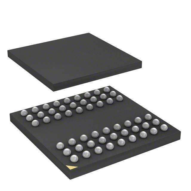
MCP6271/1R/2/3/4/5 170 µA, 2 MHz Rail-to-Rail Op Amp Features Description • Gain Bandwidth Product: 2MHz (typical) The Microchip Technology Inc. MCP6271/1R/2/3/4/5 • Supply Current: I = 170µA (typical) family of operational amplifiers (op amps) provide wide Q • Supply Voltage: 2.0V to 6.0V bandwidth for the current. This family has a 2MHz Gain Bandwidth Product (GBWP) and a 65° Phase • Rail-to-Rail Input/Output Margin. This family also operates from a single supply • Extended Temperature Range: –40°C to +125°C voltage as low as 2.0V, while drawing 170µA (typical) • Available in Single, Dual and Quad Packages quiescent current. The MCP6271/1R/2/3/4/5 supports • Parts with Chip Select (CS) rail-to-rail input and output swing, with a Common- - Single (MCP6273) mode input voltage range of VDD+300mV to VSS– 300mV. This family of op amps is designed with Micro- - Dual (MCP6275) chip’s advanced CMOS process. Applications The MCP6275 has a Chip Select input (CS) for dual op • Automotive amps in an 8-pin package and is manufactured by • Portable Equipment cascading two op amps (the output of op amp A connected to the non-inverting input of op amp B). The • Photodiode Amplifier CS input puts the device in low power mode. • Analog Filters The MCP6271/1R/2/3/4/5 family operates over the • Notebooks and PDAs Extended Temperature Range of –40°C to +125°C, • Battery Powered Systems with a power supply range of 2.0V to 6.0V. Available Tools • SPICE Macro Models • FilterLab® Software • Mindi™ Circuit Designer & Simulator • MAPS (Microchip Advanced Part Selector) • Analog Demonstration and Evaluation Boards • Application Notes Package Types MCP6271 MCP6271 MCP6271R MCP6272 PDIP, SOIC, MSOP SOT-23-5 SOT-23-5 PDIP, SOIC, MSOP NC 1 8 NC V 1 5 V V 1 5 V V 1 8 V OUT DD OUT SS OUTA DD VIN– 2 – 7 VDD VSS 2 + – VDD 2 + – VINA– 2 –+ 7 VOUTB V + 3 + 6 V V + 3 4 V – V + 3 4 V – V + 3 –+ 6 V – IN OUT IN IN IN IN INA INB V 4 5 NC V 4 5 V + SS SS INB MCP6273 MCP6273 MCP6274 MCP6275 PDIP, SOIC, MSOP SOT-23-6 PDIP, SOIC, TSSOP PDIP, SOIC, MSOP NC 1 8 CS V 1 6 V V 1 14V V /V + 1 8 V OUT DD OUTA OUTD OUTA INB DD VIN– 2 – 7 VDD VSS 2 +– 5 CS VINA– 2 –+ +– 13VIND– VINA– 2 –+ 7 VOUTB V + 3 + 6 V V + 3 4 V – V + 3 12V + V + 3 +– 6 V – IN OUT IN IN INA IND INA INB V 4 5 NC V 4 11 V V 4 5 CS SS DD SS SS V + 5 10V + INB INC VINB– 6 –+ +– 9 VINC– VOUTB 7 8 VOUTC 2019 Microchip Technology Inc. DS20001810G-page 1
MCP6271/1R/2/3/4/5 NOTES: DS20001810G-page 2 2019 Microchip Technology Inc.
MCP6271/1R/2/3/4/5 1.0 ELECTRICAL † Notice: Stresses above those listed under “Absolute Maximum Ratings” may cause permanent damage to the CHARACTERISTICS device. This is a stress rating only and functional operation of the device at those or any other conditions above those Absolute Maximum Ratings † indicated in the operational listings of this specification is not implied. Exposure to maximum rating conditions for extended VDD–VSS........................................................................7.0V periods may affect device reliability. Current at Input Pins ....................................................±2mA †† See Section4.1.2 “Input Voltage and Current Limits”. Analog Inputs (V + and V –)††..V –1.0VtoV +1.0V IN IN SS DD All other Inputs and Outputs ..........V –0.3V to V +0.3V SS DD Difference Input Voltage ......................................|V –V | DD SS Output Short Circuit Current ................................Continuous Current at Output and Supply Pins ............................±30mA Storage Temperature...................................–65°C to +150°C Junction Temperature (T ) .........................................+150°C J ESD Protection On All Pins (HBM/MM) 4kV/400V DC ELECTRICAL SPECIFICATIONS Electrical Characteristics: Unless otherwise indicated, T =+25°C, V =+2.0V to +5.5V, V =GND, V =V /2, A DD SS CM DD V V /2, V = V /2, R =10kto V and CS is tied low. (Refer to Figure1-2 and Figure1-3). OUT DD L DD L L Parameters Sym Min Typ Max Units Conditions Input Offset (Note1) Input Offset Voltage V –3.0 — +3.0 mV V = V OS CM SS Input Offset Voltage V –5.0 — +5.0 mV T = –40°C to +125°C, V = V OS A CM SS (Extended Temperature) Input Offset Temperature Drift V /T — ±1.7 — µV/°C T = –40°C to +125°C, V = V OS A A CM SS Power Supply Rejection Ratio PSRR 70 90 — dB V = V CM SS Input Bias Current and Impedance Input Bias Current I — ±1.0 — pA Note2 B At Temperature I — 50 200 pA T = +85°C (Note2) B A At Temperature I — 2 5 nA T = +125°C (Note2) B A Input Offset Current I — ±1.0 — pA Note3 OS Common-mode Input Impedance Z — 1013||6 — ||pF Note3 CM Differential Input Impedance Z — 1013||3 — ||pF Note3 DIFF Common-mode (Note4) Common-mode Input Voltage Range V V 0.15 — V +0.15 V V = 2.0V (Note5) CMR SS DD DD V V 0.30 — V +0.30 V V = 5.5V (Note5) CMR SS DD DD Common-mode Rejection Ratio CMRR 70 85 — dB V = –0.3V to 2.5V, V = 5V CM DD (Note6) Common-mode Rejection Ratio CMRR 65 80 — dB V = –0.3V to 5.3V, V = 5V CM DD (Note6) Open-Loop Gain DC Open-Loop Gain (Large Signal) A 90 110 — dB V = 0.2V to V – 0.2V, OL OUT DD V =V (Note1) CM SS Note 1: The MCP6275’s V for op amp B (pins V /V + and V –) is V +100mV. CM OUTA INB INB SS 2: The current at the MCP6275’s V – pin is specified by I only. INB B 3: This specification does not apply to the MCP6275’s V /V + pin. OUTA INB 4: The MCP6275’s V – pin (op amp B) has a Common-mode input voltage range (V ) of V +100mV to INB CMR SS V –100mV. CMRR is not measured for op amp B of the MCP6275. The MCP6275’s V /V + pin (op amp B) DD OUTA INB has a voltage range specified by V and V . OH OL 5: Set by design and characterization. 6: Does not apply to op amp B of the MCP6275. 7: All parts with date codes November 2007 and later have been screened to ensure operation at V = 6.0V. However, DD the other minimum and maximum specifications are measured at 2.0V and 5.5V. 2019 Microchip Technology Inc. DS20001810G-page 3
MCP6271/1R/2/3/4/5 DC ELECTRICAL SPECIFICATIONS (CONTINUED) Electrical Characteristics: Unless otherwise indicated, T =+25°C, V =+2.0V to +5.5V, V =GND, V =V /2, A DD SS CM DD V V /2, V = V /2, R =10kto V and CS is tied low. (Refer to Figure1-2 and Figure1-3). OUT DD L DD L L Parameters Sym Min Typ Max Units Conditions Output Maximum Output Voltage Swing V , V V +15 — V 15 mV 0.5V input overdrive (Note4) OL OH SS DD Output Short Circuit Current I — ±25 — mA SC Power Supply Supply Voltage V 2.0 — 6.0 V DD Quiescent Current per Amplifier I 100 170 240 µA I = 0 Q O Note 1: The MCP6275’s V for op amp B (pins V /V + and V –) is V +100mV. CM OUTA INB INB SS 2: The current at the MCP6275’s V – pin is specified by I only. INB B 3: This specification does not apply to the MCP6275’s V /V + pin. OUTA INB 4: The MCP6275’s V – pin (op amp B) has a Common-mode input voltage range (V ) of V +100mV to INB CMR SS V –100mV. CMRR is not measured for op amp B of the MCP6275. The MCP6275’s V /V + pin (op amp B) DD OUTA INB has a voltage range specified by V and V . OH OL 5: Set by design and characterization. 6: Does not apply to op amp B of the MCP6275. 7: All parts with date codes November 2007 and later have been screened to ensure operation at V = 6.0V. However, DD the other minimum and maximum specifications are measured at 2.0V and 5.5V. AC ELECTRICAL SPECIFICATIONS Electrical Characteristics: Unless otherwise indicated, T =+25°C, V =+2.0V to +5.5V, V =GND, V =V /2, A DD SS CM DD V V /2, V = V /2, R =10kto V , C =60pF and CS is tied low. (Refer to Figure1-2 and Figure1-3). OUT DD L DD L L L Parameters Sym Min Typ Max Units Conditions AC Response Gain Bandwidth Product GBWP — 2.0 — MHz Phase Margin PM — 65 — ° G = +1V/V Slew Rate SR — 0.9 — V/µs Noise Input Noise Voltage E — 4.6 — µV f = 0.1Hz to 10Hz ni P-P Input Noise Voltage Density e — 20 — nV/Hz f = 1kHz ni Input Noise Current Density i — 3 — fA/Hz f = 1kHz ni CS V V IL IH t t OFF ON High-Z High-Z V OUT -0.7µA -0.7µA (typical) -170µA (typical) I (typical) SS 0.7µA 0.7µA (typical) 10nA (typical) (typical) I CS FIGURE 1-1: Timing Diagram for the Chip Select (CS) pin on the MCP6273 and MCP6275. DS20001810G-page 4 2019 Microchip Technology Inc.
MCP6271/1R/2/3/4/5 TEMPERATURE SPECIFICATIONS Electrical Characteristics: Unless otherwise indicated, V =+2.0V to +5.5V and V =GND. DD SS Parameters Sym Min Typ Max Units Conditions Temperature Ranges Specified Temperature Range T –40 — +125 °C A Operating Temperature Range T –40 — +125 °C Note A Storage Temperature Range T –65 — +150 °C A Thermal Package Resistances Thermal Resistance, 5L-SOT-23 — 256 — °C/W JA Thermal Resistance, 6L-SOT-23 — 230 — °C/W JA Thermal Resistance, 8L-PDIP — 85 — °C/W JA Thermal Resistance, 8L-SOIC — 163 — °C/W JA Thermal Resistance, 8L-MSOP — 206 — °C/W JA Thermal Resistance, 14L-PDIP — 70 — °C/W JA Thermal Resistance, 14L-SOIC — 120 — °C/W JA Thermal Resistance, 14L-TSSOP — 100 — °C/W JA Note: The Junction Temperature (T ) must not exceed the Absolute Maximum specification of +150°C. J MCP6273/MCP6275 CHIP SELECT SPECIFICATIONS Electrical Characteristics: Unless otherwise indicated, T =+25°C, V =+2.0V to +5.5V, V =GND, A DD SS V =V /2, V V /2, V = V /2, R =10kto V /2, C =60pF and CS is tied low. CM DD OUT DD L DD L DD L Parameters Sym Min Typ Max Units Conditions CS Low Specifications CS Logic Threshold, Low V V — 0.2V V IL SS DD CS Input Current, Low I — 0.01 — µA CS = V CSL SS CS High Specifications CS Logic Threshold, High V 0.8V — V V IH DD DD CS Input Current, High I — 0.7 2 µA CS = V CSH DD GND Current per Amplifier I — –0.7 — µA CS = V SS DD Amplifier Output Leakage — — 0.01 — µA CS = V DD Dynamic Specifications (Note1) CS Low to Valid Amplifier t — 4 10 µs CS Low 0.2V , G = +1V/V, ON DD Output, Turn on Time V = V /2, V = 0.9V /2, IN DD OUT DD V = 5.0V DD CS High to Amplifier Output t — 0.01 — µs CS High 0.8V , G = +1V/V, OFF DD High-Z V = V /2, V = 0.1V /2 IN DD OUT DD Hysteresis V — 0.6 — V V = 5V HYST DD Note 1: The input condition (V ) specified applies to both op amp A and B of the MCP6275. The dynamic IN specification is tested at the output of op amp B (V ). OUTB 2019 Microchip Technology Inc. DS20001810G-page 5
MCP6271/1R/2/3/4/5 1.1 Test Circuits The test circuits used for the DC and AC tests are shown in Figure1-2 and Figure1-3. The bypass capacitors are laid out according to the rules discussed in Section4.7 “Supply Bypass”. VDD 1µF V 0.1µF IN RN VOUT MCP627X C R L L VDD/2 RG RF V L FIGURE 1-2: AC and DC Test Circuit for Most Non-Inverting Gain Conditions. VDD 1µF V /2 0.1µF DD RN VOUT MCP627X C R L L VIN RG RF V L FIGURE 1-3: AC and DC Test Circuit for Most Inverting Gain Conditions. DS20001810G-page 6 2019 Microchip Technology Inc.
MCP6271/1R/2/3/4/5 2.0 TYPICAL PERFORMANCE CURVES Note: The graphs and tables provided following this note are a statistical summary based on a limited number of samples and are provided for informational purposes only. The performance characteristics listed herein are not tested or guaranteed. In some graphs or tables, the data presented may be outside the specified operating range (e.g., outside specified power supply range) and therefore outside the warranted range. Note: Unless otherwise indicated, T =+25°C, V =+2.0V to +5.5V, V =GND, V =V /2, V V /2, A DD SS CM DD OUT DD V = V /2, R =10k to V , C =60pF and CS is tied low. L DD L L L 18% 14% Occurrences 11110246%%%% 8V3C2M S= aVmSSples Occurrences 11028%%% 8VT3AC 2M= S=-4 aV0mS°SpCl etos +125°C Percentage of 02468%%%%% Percentage of 246%%% 0% 0 4 8 2 6 0 6 2 8 4 0 -3. -2. -1. -1. -0. 0. 0. 1. 1. 2. 3. -10 -8 -6 -4 -2 0 2 4 6 8 10 Input Offset Voltage (mV) Input Offset Voltage Drift (µV/°C) FIGURE 2-1: Input Offset Voltage. FIGURE 2-4: Input Offset Voltage Drift. 32% 22% ces28% 4T2A 2= S8a5m°Cples es 1280%% 4T2A 2= S+a1m25p°lCes en24% nc 16% curr20% urre 14% c c 12% entage of O11268%%% ntage of Oc 10468%%%% Perc 04%% Perce 02%% 6 8 0 2 4 6 8 0 2 4 6 8 0 0 10 20 30 40 50 60 70 80 90 100 0. 0. 1. 1. 1. 1. 1. 2. 2. 2. 2. 2. 3. Input Bias Current (pA) Input Bias Current (nA) FIGURE 2-2: Input Bias Current at FIGURE 2-5: Input Bias Current at T =+85°C. T =+125°C. A A 300 300 V = 2.0V V = 5.5V V) 250 DD V) 250 DD µ µ e ( 200 e ( 200 g g olta 150 olta 150 TA = +125°C V 100 V 100 ut Offset 500 TTTAAA === + ++1282555°°°CCC ut Offset 500 TTAA == ++8255°°CC np -50 TA = -40°C np -50 TA = -40°C I I -100 -100 -0.4 -0.2 0.0 0.2 0.4 0.6 0.8 1.0 1.2 1.4 1.6 1.8 2.0 2.2 2.4 -0.5 0.0 0.5 1.0 1.5 2.0 2.5 3.0 3.5 4.0 4.5 5.0 5.5 6.0 Common Mode Input Voltage (V) Common Mode Input Voltage (V) FIGURE 2-3: Input Offset Voltage vs. FIGURE 2-6: Input Offset Voltage vs. Common-mode Input Voltage, with V =2.0V. Common-mode Input Voltage, with V =5.5V. DD DD 2019 Microchip Technology Inc. DS20001810G-page 7
MCP6271/1R/2/3/4/5 Note: Unless otherwise indicated, T =+25°C, V =+2.0V to +5.5V, V =GND, V =V /2, V V /2, A DD SS CM DD OUT DD V = V /2, R =10k to V , C =60pF and CS is tied low. L DD L L L age -00..0050 Typical lower (VCM – VSS) limit age 00..4550 olt -0.10 olt 0.40 VDD = 5.5V nput Vmit (V) --00..2105 VDD = 2.0V nput Vmit (V) 00..3305 e ILi -0.25 e ILi 0.25 mon ModRange ---000...433050 VDD = 5.5V mon ModRange 000...112050 VDD = 2.0V m m o -0.45 o 0.05 Typical upper (VCM – VDD) limit C -0.50 C 0.00 -50 -25 0 25 50 75 100 125 -50 -25 0 25 50 75 100 125 Ambient Temperature (°C) Ambient Temperature (°C) FIGURE 2-7: Common-mode Input FIGURE 2-10: Common-mode Input Voltage Range Lower Limit vs. Temperature. Voltage Range Upper Limit vs. Temperature. 300 V = V 10,000 nput Offset Voltage (µV) 1122-0505550000000 VDD = 2.0V RCeMprVeDsDeS nS= t5a.t5ivVe Part ut Bias, Offset Currents(pA) 1,10001000 VVICDnMDp ==u t5V B.D5iDVas CurreInntput Offset Current I p -100 In 1 0.0 0.5 1.0 1.5 2.0 2.5 3.0 3.5 4.0 4.5 5.0 5.5 45 55 65 75 85 95 105 115 125 Output Voltage (V) Ambient Temperature (°C) FIGURE 2-8: Input Offset Voltage vs. FIGURE 2-11: Input Bias, Input Offset Output Voltage. Currents vs. Temperature. 110 120 100 CMRR 110 SRR (dB) 789000 MRR (dB)10900 CMRR P 60 PSRR– C MRR, 50 PSRR+ SRR, 80 (VCPMS =R VRSS) C 40 P 70 30 60 20 1.E1+00 1.E1+001 1.1E0+002 1.E1+k03 1.1E0+k04 11.E0+00k5 1.E1M+06 -50 -25 0 25 50 75 100 125 Frequency (Hz) Ambient Temperature (°C) FIGURE 2-9: CMRR, PSRR vs. FIGURE 2-12: CMRR, PSRR vs. Frequency. Temperature. DS20001810G-page 8 2019 Microchip Technology Inc.
MCP6271/1R/2/3/4/5 Note: Unless otherwise indicated, T =+25°C, V =+2.0V to +5.5V, V =GND, V =V /2, V V /2, A DD SS CM DD OUT DD V = V /2, R =10k to V , C =60pF and CS is tied low. L DD L L L 55 2.5 Input Bias, Offset Currents(pA) --123421-55555555 TVAD D= = 8 55.°5CV InInppuut tO Bfifasse tC Cuurrrerenntt Input Bias, Offset Currents(nA)--0011210.......0505050 TVAD D= = 1 52.55°VC InInppuutt O Bfifasse tC Cuurrrerenntt 0.0 0.5 1.0 1.5 2.0 2.5 3.0 3.5 4.0 4.5 5.0 5.5 0.0 0.5 1.0 1.5 2.0 2.5 3.0 3.5 4.0 4.5 5.0 5.5 Common Mode Input Voltage (V) Common Mode Input Voltage (V) FIGURE 2-13: Input Bias, Offset Currents FIGURE 2-16: Input Bias, Offset Currents vs. Common-mode Input Voltage, with vs. Common-mode Input Voltage, with T =+85°C. T =+125°C. A A 250 1000 m nt 200 oo Quiescent Curre(µA/amplifier) 11055000 TTTTAAAA ==== +++-41820255°5°°CCC°C uput Voltage Headr(mV)10100 VOL – VSS VDD – VOH O 0 1 0.0 0.5 1.0 1.5 2.0 2.5 3.0 3.5 4.0 4.5 5.0 5.5 0.01 0.1 1 10 Power Supply Voltage (V) Output Current Magnitude (mA) FIGURE 2-14: Quiescent Current vs. FIGURE 2-17: Output Voltage Headroom Supply Voltage. vs. Output Current Magnitude. 120 0 3.0 80 op Gain (dB) 104680000 Phase Gain ----196320000 op Phase (°) width Product MHz)122...505 GBWP, VVDDDD == 52..50VV 677505 Margin (°) pen-Lo 20 -150 pen-Lo n Band(1.0 PM, VDD = 5.5V 60 Phase O 0 -180 O ai 0.5 VDD = 2.0V 55 G -20 -210 0.0 50 01.E-01.1 1.E+001 11.E+010 11.E+020F0req11.E+03uken1c1.E+040yk (H11.E+050z0)k11.E+06M101.E+07M11.E+0800M -50 -25Amb0ient 2T5empe5r0atur7e 5(°C)100 125 FIGURE 2-15: Open-Loop Gain, Phase vs. FIGURE 2-18: Gain Bandwidth Product, Frequency. Phase Margin vs. Temperature. 2019 Microchip Technology Inc. DS20001810G-page 9
MCP6271/1R/2/3/4/5 Note: Unless otherwise indicated, T =+25°C, V =+2.0V to +5.5V, V =GND, V =V /2, V V /2, A DD SS CM DD OUT DD V = V /2, R =10k to V , C =60pF and CS is tied low. L DD L L L 10 1.8 ximum Output Voltage Swing (V)P-P 1 VVDDDD == 25..05VV Slew Rate (V/µs) 0001111.......4680246 Falling EdgeRising EdVgDeD =V 5DD.5 =V 2.0V a M 0.2 0.1 0.0 1+03k 1+040k 10+050k 1+06M 10+07M -50 -25 0 25 50 75 100 125 1.E 1.E Freque1.Ency (Hz) 1.E 1.E Ambient Temperature (°C) FIGURE 2-19: Maximum Output Voltage FIGURE 2-22: Slew Rate vs. Temperature. Swing vs. Frequency. 1,000 25 y ensity Densit 20 D e oltage Hz)(cid:151) 100 VoltagV/Hz)(cid:165) 15 VV/ e n 10 se (n ois( nput Noi Input N 05 fV =DD 1 = k 5H.z0V I 10 10..E1- 1.1E+ 11.E0+ 11.0E0+ 11.Ek+ 11.0Ek+ 110.E0+k 11.EM+ 0.5 0.0 0.5 1.0 1.5 2.0 2.5 3.0 3.5 4.0 4.5 5.0 5.5 - 01 00 01Freq02uenc0y3 (Hz)04 05 06 Common Mode Input Voltage (V) FIGURE 2-20: Input Noise Voltage Density FIGURE 2-23: Input Noise Voltage Density vs. Frequency. vs. Common-mode Input Voltage, with f=1kHz. 35 140 Current 2350 nnelB) 130 Short-Circuit (mA) 112050 TTTA AA= == + ++1282555°°°CCC hannel-to-ChaSeparation (d 111200 ut 5 TA = -40°C C pt u O 0 100 0.0 0.5 1.0 1.5 2.0 2.5 3.0 3.5 4.0 4.5 5.0 5.5 1 10 100 Power Supply Voltage (V) Frequency (kHz) FIGURE 2-21: Output Short Circuit Current FIGURE 2-24: Channel-to-Channel vs. Supply Voltage. Separation vs. Frequency (MCP6272 and MCP6274). DS20001810G-page 10 2019 Microchip Technology Inc.
MCP6271/1R/2/3/4/5 Note: Unless otherwise indicated, T =+25°C, V =+2.0V to +5.5V, V =GND, V =V /2, V V /2, A DD SS CM DD OUT DD V = V /2, R =10k to V , C =60pF and CS is tied low. L DD L L L 250 700 VDD = 2.0V Op Amp turns Off 600 VDD = 5.5V Hysteresis nt Currentmplifier) 125000 Op Amp turns On Hysteresis nt Currentmplifier) 450000 w CLoSw s-wtoe-pHtigh Quiesce(µA/a 10500 CHiSg hsw-toe-pLtow CLoSw s-wtoe-pHtigh Quiesce(µA/a 123000000 CS sweptHigh-to-Lo OOtpun rA/nOmsffp 0 0 0.0 0.2 0.4 0.6 0.8 1.0 1.2 1.4 1.6 1.8 2.0 0.0 0.5 1.0 1.5 2.0 2.5 3.0 3.5 4.0 4.5 5.0 5.5 Chip Select Voltage (V) Chip Select Voltage (V) FIGURE 2-25: Quiescent Current vs. Chip FIGURE 2-28: Quiescent Current vs. Chip Select (CS) Voltage, with V =2.0V (MCP6273 Select (CS) Voltage, with V =5.5V (MCP6273 DD DD and MCP6275 only). and MCP6275 only). 5.0 5.0 4.5 G = +1 V/V 4.5 G = -1 V/V 4.0 VDD = 5.0V 4.0 VDD = 5.0V e (V) 3.5 e (V) 3.5 g 3.0 g 3.0 a a olt 2.5 olt 2.5 V V ut 2.0 ut 2.0 p p ut 1.5 ut 1.5 O O 1.0 1.0 0.5 0.5 0.0 0.0 Time (5 µs/div) Time (5 µs/div) FIGURE 2-26: Large Signal Non-inverting FIGURE 2-29: Large Signal Inverting Pulse Pulse Response. Response. G = +1 V/V G = -1 V/V v) v) di di V/ V/ m m 0 0 1 1 e ( e ( g g a a olt olt V V ut ut p p ut ut O O Time (2 µs/div) Time (2 µs/div) FIGURE 2-27: Small Signal Non-inverting FIGURE 2-30: Small Signal Inverting Pulse Pulse Response. Response. 2019 Microchip Technology Inc. DS20001810G-page 11
MCP6271/1R/2/3/4/5 Note: Unless otherwise indicated, T =+25°C, V =+2.0V to +5.5V, V =GND, V =V /2, V V /2, A DD SS CM DD OUT DD V = V /2, R =10k to V , C =60pF and CS is tied low. L DD L L L 2.5 6.0 Chip Select, Output Voltages(V) 0112....5050 OutpuVCtO SHUTigh-Z OVGVuDI Nt=Dp = u=+ V t12 OS.VS0n/VV Chip Select, Output Voltages(V) 01122334455...........50505050505 OutputV CHOSUigTh-Z OuVGVtpDI N=Du = t=+ OV 15 Sn.VS5/VV 0.0 0.0 Time (5 µs/div) Time (5 µs/div) FIGURE 2-31: Chip Select (CS) to FIGURE 2-33: Chip Select (CS) to Amplifier Output Response Time, with Amplifier Output Response Time, with V =2.0V (MCP6273 and MCP6275 only). V =5,5V (MCP6273 and MCP6275 only). DD DD 1.E1-00m2 6 Magnitude (A)11111.....11EEEEE001-----1000000100m76543nµµµ Voltage (V) 345 VGD =D =+ 25 .V0/VV Input Current 11111.....1EEEEE011-----111000001121098pnpnp +++1-42820555°°°°CCCC Input, Output 012 VOUT VIN -1.0 -0.9 -0.8 -0.7 -0.6 -0.5 -0.4 -0.3 -0.2 -0.1 0.0 -1 Input Voltage (V) Time (1 ms/div) FIGURE 2-32: Input Current vs. Input FIGURE 2-34: The MCP6271/1R/2/3/4/5 Voltage. Show no Phase Reversal. DS20001810G-page 12 2019 Microchip Technology Inc.
MCP6271/1R/2/3/4/5 3.0 PIN DESCRIPTIONS Descriptions of the pins are listed in Table3-1 (single op amps) and Table3-2 (dual and quad op amps). TABLE 3-1: PIN FUNCTION TABLE FOR SINGLE OP AMPS MCP6271 MCP6271R MCP6273 Symbol Description PDIP, SOIC, PDIP, SOIC, SOT-23-5 SOT-23-5 SOT-23-6 MSOP MSOP 2 4 4 2 4 V – Inverting Input IN 3 3 3 3 3 V + Non-inverting Input IN 4 2 5 4 2 V Negative Power Supply SS 6 1 1 6 1 V Analog Output OUT 7 5 2 7 6 V Positive Power Supply DD — — — 8 5 CS Chip Select 1,5,8 — — 1,5 — NC No Internal Connection TABLE 3-2: PIN FUNCTION TABLE FOR DUAL AND QUAD OP AMPS MCP6272 MCP6274 MCP6275 Symbol Description 1 1 — V Analog Output (op amp A) OUTA 2 2 2 V – Inverting Input (op amp A) INA 3 3 3 V + Non-inverting Input (op amp A) INA 8 4 8 V Positive Power Supply DD 5 5 — V + Non-inverting Input (op amp B) INB 6 6 6 V – Inverting Input (op amp B) INB 7 7 7 V Analog Output (op amp B) OUTB — 8 — V Analog Output (op amp C) OUTC — 9 — V – Inverting Input (op amp C) INC — 10 — V + Non-inverting Input (op amp C) INC 4 11 4 V Negative Power Supply SS — 12 — V + Non-inverting Input (op amp D) IND — 13 — V – Inverting Input (op amp D) IND — 14 — V Analog Output (op amp D) OUTD — — 1 V /V + Analog Output (op amp A)/Non-inverting Input (op amp B) OUTA INB — — 5 CS Chip Select 3.1 Analog Outputs 3.4 Chip Select Digital Input The output pins are low impedance voltage sources. This is a CMOS, Schmitt triggered input that places the part into a low power mode of operation. 3.2 Analog Inputs 3.5 Power Supply Pins The non-inverting and inverting inputs are high impedance CMOS inputs with low bias currents. The positive power supply (V ) is 2.0V to 6.0V higher DD than the negative power supply (V ). For normal SS 3.3 MCP6275’s VOUTA/VINB+ Pin operation, the other pins are at voltages between VSS and V . DD For the MCP6275 only, the output of op amp A is Typically, these parts are used in a single (positive) connected directly to the non-inverting input of op amp supply configuration. In this case, V is connected to B; this is the V /V + pin. This connection makes SS OUTA INB ground and V is connected to the supply. V will it possible to provide a CS pin for duals in 8-pin DD DD need bypass capacitors. packages. 2019 Microchip Technology Inc. DS20001810G-page 13
MCP6271/1R/2/3/4/5 4.0 APPLICATION INFORMATION dump any currents onto V . When implemented as DD shown, resistors R and R also limit the current 1 2 The MCP6271/1R/2/3/4/5 family of op amps is through D and D . 1 2 manufactured using Microchip’s state of the art CMOS process, specifically designed for low cost, low power and general purpose applications. The low supply VDD voltage, low quiescent current and wide bandwidth make the MCP6271/1R/2/3/4/5 ideal for battery D powered applications. 1 V 1 4.1 Rail-to-Rail Inputs R 1 D2 MCP627X VOUT V 4.1.1 PHASE REVERSAL 2 R 2 The input devices are designed to not exhibit phase inversion when the input pins exceed the supply voltages. Figure2-34 shows an input voltage R 3 exceeding both supplies with no phase inversion. V –(minimum expected V ) SS 1 R > 4.1.2 INPUT VOLTAGE AND CURRENT 1 2mA LIMITS V –(minimum expected V ) SS 2 R > The ESD protection on the inputs can be depicted as 2 2mA shown in Figure4-1. This structure was chosen to FIGURE 4-2: Protecting the Analog protect the input transistors, and to minimize input bias current (I ). The input ESD diodes clamp the inputs Inputs. B when they try to go more than one diode drop below It is also possible to connect the diodes to the left of the V . They also clamp any voltages that go too far SS resistor R and R . In this case, the currents through 1 2 above V ; their breakdown voltage is high enough to DD the diodes D and D need to be limited by some other 1 2 allow normal operation, and low enough to bypass mechanism. The resistors then serve as in-rush current quick ESD events within the specified limits. limiters; the DC current into the input pins (V + and IN V –) should be very small. IN Bond A significant amount of current can flow out of the V DD Pad inputs (through the ESD diodes) when the Common- mode voltage (V ) is below ground (V ); see CM SS Figure2-32. Applications that are high impedance may need to limit the usable voltage range. Bond Input Bond V + V – IN Pad Stage Pad IN 4.1.3 NORMAL OPERATIONS The input stage of the MCP6271/1R/2/3/4/5 op amps uses two differential CMOS input stages in parallel. Bond V One operates at low Common-mode input voltage SS Pad (V and the other at high V . With this topology, the CM CM input operates with V up to 0.3V past either supply CM FIGURE 4-1: Simplified Analog Input ESD rail (see Figure2-7 and Figure2-10). The input offset Structures. voltage (V ) is measured at V =V –0.3V and OS CM SS V +0.3V to ensure proper operation. In order to prevent damage and/or improper operation DD of these amplifiers, the circuit must limit the currents The transition between the two input stage occurs (and voltages) at the input pins (see Absolute Maxi- when V V –1.1V (see Figure2-3 and Figure2- CM DD mum Ratings † at the beginning of Section1.0 “Elec- 6). For the best distortion and gain linearity, with non- trical Characteristics”). Figure4-2 shows the inverting gains, avoid this region of operation. recommended approach to protecting these inputs. The internal ESD diodes prevent the input pins (V + 4.2 Rail-to-Rail Output IN and V –) from going too far below ground, and the IN resistors R and R limit the possible current drawn out The output voltage range of the MCP6271/1R/2/3/4/5 1 2 of the input pins. Diodes D1 and D2 prevent the input op amps is VDD–15mV (minimum) and VSS+15mV pins (VIN+ and VIN–) from going too far above VDD, and (maximum) when RL=10k is connected to VDD/2 and V =5.5V. Refer to Figure2-17 for more informa- DD tion. DS20001810G-page 14 2019 Microchip Technology Inc.
MCP6271/1R/2/3/4/5 4.3 Capacitive Loads 4.4 MCP6273/5 Chip Select Driving large capacitive loads can cause stability The MCP6273 and MCP6275 are single and dual op problems for voltage feedback op amps. As the load amps with Chip Select (CS), respectively. When CS is capacitance increases, the feedback loop’s phase pulled high, the supply current drops to 0.7µA (typical) margin decreases and the closed-loop bandwidth is and flows through the CS pin to V . When this SS reduced. This produces gain peaking in the frequency happens, the amplifier output is put into a high response, with overshoot and ringing in the step impedance state. By pulling CS low, the amplifier is response. A unity gain buffer (G=+1) is the most enabled. The CS pin has an internal 5M (typical) pull- sensitive to capacitive loads, though all gains show the down resistor connected to V , so it will go low if the SS same general behavior. CS pin is left floating. Figure1-1 shows the output volt- age and supply current response to a CS pulse. When driving large capacitive loads with these op amps (e.g., >100pF when G=+1), a small series 4.5 Cascaded Dual Op Amps resistor at the output (R in Figure4-3) improves the ISO feedback loop’s phase margin (stability) by making the (MCP6275) output load resistive at higher frequencies. The The MCP6275 is a dual op amp with Chip Select (CS). bandwidth will be generally lower than the bandwidth The Chip Select input is available on what would be the with no capacitive load. non-inverting input of a standard dual op amp (pin 5). This pin is available because the output of op amp A connects to the non-inverting input of op amp B, as _ R shown in Figure4-5. The Chip Select input, which can ISO be connected to a microcontroller I/O line, puts the MCP627X VOUT device in low power mode. Refer to Section4.4 VIN + C “MCP6273/5 Chip Select (CS)”. L FIGURE 4-3: Output Resistor, R VOUTA/VINB+ VINB– ISO stabilizes large capacitive loads. 1 6 _ Fdiifgfeurreen4t -c4a pgaicvietisv e rloeacdosm amnedn dgeadin s.R TIShOe xv-aaxluise sis tfhoer VINA– 2 _ B 7 VOUTB A + normalized load capacitance (C /G ), where G is the 3 L N N V + + INA circuit's noise gain. For non-inverting gains, G and the N MCP6275 Signal Gain are equal. For inverting gains, G is N 1+|Signal Gain| (e.g., –1V/V gives G =+2 V/V). N 5 CS 1,000 FIGURE 4-5: Cascaded Gain Amplifier. )(cid:58) (O The output of op amp A is loaded by the input S RI d impedance of op amp B, which is typically de 100 10136pF, as specified in the DC specification table n me (Refer to Section4.3 “Capacitive Loads” for further m GN = 1 V/V details regarding capacitive loads). o G = 2 V/V c N Re GN(cid:116) 4 V/V The Common-mode input range of these op amps is 10 specified in the data sheet as VSS–300mV and 10 100 1,000 10,000 V +300mV. However, since the output of op amp A DD Normalized Load Capacitance; C / G (pF) is limited to V and V (20mV from the rails with a L N OL OH 10k load), the non-inverting input range of op amp B FIGURE 4-4: Recommended R Values ISO is limited to the Common-mode input range of for Capacitive Loads. V +20mV and V –20mV. SS DD After selecting R for your circuit, double check the ISO resulting frequency response peaking and step response overshoot. Modify R 's value until the ISO response is reasonable. Bench evaluation and simulations with the MCP6271/1R/2/3/4/5 SPICE macro model are helpful. 2019 Microchip Technology Inc. DS20001810G-page 15
MCP6271/1R/2/3/4/5 4.6 Unused Amplifiers V – V + IN IN V An unused op amp in a quad package (MCP6274) SS should be configured as shown in Figure4-6. These circuits prevent the output from toggling and causing crosstalk. In CircuitA, R and R produce a voltage 1 2 within its output voltage range (V , V ). The op amp OH OL buffers this voltage, which can be used elsewhere in the circuit. CircuitB uses the minimum number of components and operates as a comparator. Guard Ring ¼MCP6274(A) ¼MCP6274(B) FIGURE 4-7: Example Guard Ring Layout for Inverting Gain. V V DD DD 1. For Inverting Gain and Transimpedance VDD Amplifiers (convert current to voltage, such as R 1 photo detectors): + + a) Connect the guard ring to the non-inverting V – REF input pin (V +). This biases the guard ring R – IN 2 to the same reference voltage as the op amp (e.g., V /2 or ground). DD b) Connect the inverting pin (V –) to the input IN R with a wire that does not touch the PCB VREF = VDDR--------+---2--R----- surface. 1 2 2. Non-inverting Gain and Unity Gain Buffer: FIGURE 4-6: Unused Op Amps. a) Connect the non-inverting pin (VIN+) to the input with a wire that does not touch the PCB surface. 4.7 Supply Bypass b) Connect the guard ring to the inverting input With this family of operational amplifiers, the power pin (V –). This biases the guard ring to the IN supply pin (V for single supply) should have a local Common-mode input voltage. DD bypass capacitor (i.e., 0.01µF to 0.1µF) within 2mm for good, high frequency performance. It also needs a bulk capacitor (i.e., 1µF or larger) within 100mm to provide large, slow currents. This bulk capacitor can be shared with nearby analog parts. 4.8 PCB Surface Leakage In applications where low input bias current is critical, Printed Circuit Board (PCB) surface leakage effects need to be considered. Surface leakage is caused by humidity, dust or other contamination on the board. Under low humidity conditions, a typical resistance between nearby traces is 1012. A 5V difference would cause 5pA of current to flow. This is greater than the MCP6271/1R/2/3/4/5 family’s bias current at 25°C (1pA, typical). The easiest way to reduce surface leakage is to use a guard ring around sensitive pins (or traces). The guard ring is biased at the same voltage as the sensitive pin. An example of this type of layout is illustrated in Figure4-7. DS20001810G-page 16 2019 Microchip Technology Inc.
MCP6271/1R/2/3/4/5 4.9 Application Circuits 4.9.2 LOSSY NON-INVERTING INTEGRATOR 4.9.1 ACTIVE FULL-WAVE RECTIFIER The non-inverting integrator shown in Figure4-9 is The MCP6271/1R/2/3/4/5 family of amplifiers can be easy to build. It saves one op amp over the typical used in applications such as an Active Full-Wave Miller integrator plus inverting amplifier configuration. Rectifier or an Absolute Value circuit, as shown in The phase accuracy of this integrator depends on the Figure4-8. The amplifier and feedback loops in this matching of the input and feedback resistor-capacitor active voltage rectifier circuit eliminate the diode drop time constants. R makes this a lossy integrator (it has F problem that exists in a passive voltage rectifier. This finite gain at DC) and stable by itself. circuit behaves as a follower (the output follows the input) as long as the input signal is more positive than R the reference voltage. If the input signal is more 1 negative than the reference voltage, however, the VIN + circuit behaves as an inverting amplifier. Therefore, the C MCP6271 VOUT 1 output voltage will always be above the reference _ voltage, regardless of the input signal. R F R 2 CC 22 VIN R1 – R R R2 F 2 Op Amp B R C =R ||R C R3 R5 + VOUT 1 1 2 F 2 1/2 R4 MCP6272 V----O----U----T----------1----------- f-------------------------1-------------------------- V sR C 2R C 1+R R IN 1 1 1 1 F 2 V REF D 1 FIGURE 4-9: Non-Inverting Integrator. D 2 R = R = R 1 2 3 – V R <R 1–-------------D----1----------- Op Amp A 4 3 V –V REF SS + R R 1/2 R = ----2-------4- VREF MCP6272 5 2R3 Input Output V V REF REF time time FIGURE 4-8: Active Full-wave Rectifier. The design equations give a gain of ±1 from V to IN V , and produce rail-to-rail outputs. OUT 2019 Microchip Technology Inc. DS20001810G-page 17
MCP6271/1R/2/3/4/5 4.9.3 CASCADED OP AMP APPLICATIONS R R R R 4 3 2 1 The MCP6275 provides the flexibility of Low power mode for dual op amps in an 8-pin package. The – MCP6275 eliminates the added cost and space in a – B VOUT battery powered application by using two single op A + amps with Chip Select (CS) lines or a 10-pin device VIN + MCP6275 with one CS line for both op amps. Since the two op amps are internally cascaded, this device cannot be used in circuits that require active or passive elements CS between the two op amps. However, there are several applications where this op amp configuration with a CS FIGURE 4-11: Cascaded Gain Circuit line becomes suitable. The circuits below show Configuration. possible applications for this device. 4.9.3.3 Difference Amplifier 4.9.3.1 Load Isolation Figure4-12 shows op amp A configured as a difference With the cascaded op amp configuration, op amp B can amplifier with Chip Select. In this configuration, it is be used to isolate the load from op amp A. In recommended that well matched resistors (e.g., 0.1%) applications where op amp A is driving capacitive or be used to increase the Common-mode Rejection low resistive loads in the feedback loop (such as an Ratio (CMRR). Op amp B can be used to provide addi- integrator or filter circuit) the op amp may not have tional gain and isolate the load from the difference sufficient source current to drive the load. In this case, amplifier. op amp B can be used as a buffer. R R R R 2 1 4 3 V – IN2 – B VOUTB A + – + MCP6275 Load R –A +B VOUT 2 VIN1 + MCP6275 CS R1 CS FIGURE 4-10: Isolating the Load with a Buffer. FIGURE 4-12: Difference Amplifier Circuit. 4.9.3.2 Cascaded Gain 4.9.3.4 Inverting Integrator with Active Figure4-11 shows a cascaded gain circuit configura- Compensation and Chip Select tion with Chip Select. Op amps A and B are configured Figure4-13 uses an active compensator (op amp B) to in a non-inverting amplifier configuration. In this compensate for the non-ideal op amp characteristics configuration, it is important to note that the input offset introduced at higher frequencies. This circuit uses voltage of op amp A is amplified by the gain of op amp opampB as a unity gain buffer to isolate the A and B, as shown below: integration capacitor C from op amp A and drives the 1 V = V G G +V G G +V G capacitor with a low impedance source. Since both op OUT IN A B OSA A B OSB B amps are matched very well, they provide a high quality Where: integrator. G = op amp A gain A GB = op amp B gain R1 C1 – VOSA = op amp A input offset voltage VIN B+ VOSB = op amp B input offset voltage – A VOUT + MCP6275 Therefore, it is recommended that you set most of the gain with op amp A and use op amp B with relatively small gain (e.g., a unity gain buffer). CS DS20001810G-page 18 2019 Microchip Technology Inc.
MCP6271/1R/2/3/4/5 FIGURE 4-13: Integrator Circuit with Active 4.9.3.7 Capacitorless Second Order Compensation. Low-Pass filter with Chip Select The low-pass filter shown in Figure4-16 does not 4.9.3.5 Second Order MFB with an Extra require external capacitors and uses only three Pole-Zero Pair external resistors; the op amp’s GBWP sets the corner Figure4-14 is a second order multiple feedback low- frequency. R and R are used to set the circuit gain. R 1 2 3 pass filter with Chip Select. Use the FilterLab® software is used to set the Q. To avoid gain peaking in the from Microchip Technology Inc. to determine the R and frequency response, Q needs to be low (lower values C values for opamp A’s second order filter. Op amp B need to be selected for R ). Note that the amplifier 3 can be used to add a pole-zero pair using C , R and bandwidth varies greatly over temperature and 3 6 R . process. This configuration, however, provides a low 7 cost solution for applications with high bandwidth requirements. R6 C3 R R2 R1 7 R1 VIN – R3 R3 R2 C1 B VOUT – V + A + IN + B VOUT – V – R A REF VDD 5 + MCP6275 MCP6275 R 4 CS CS FIGURE 4-16: Capacitorless Second Order FIGURE 4-14: Second Order Multiple Low-Pass Filter with Chip Select. Feedback Low-Pass Filter with an Extra Pole- Zero Pair. 4.9.3.6 Second Order Sallen-Key with an Extra Pole-Zero Pair Figure4-15 is a second order Sallen-Key low-pass filter with Chip Select. Use the Filterlab® software from Microchip to determine the R and C values for opampA’s second order filter. Op amp B can be used to add a pole-zero pair using C , R and R . 3 5 6 R5 C3 R 6 R R 2 1 – VOUT – B VIN R4 R3 A + + MCP6275 C C 2 1 CS FIGURE 4-15: Second Order Sallen-Key Low-Pass Filter with an Extra Pole-Zero Pair and Chip Select. 2019 Microchip Technology Inc. DS20001810G-page 19
MCP6271/1R/2/3/4/5 NOTES: DS20001810G-page 20 2019 Microchip Technology Inc.
MCP6271/1R/2/3/4/5 5.0 DESIGN TOOLS 5.5 Analog Demonstration and Evaluation Boards Microchip provides the basic design tools needed for the MCP6271/1R/2/3/4/5 family of op amps. Microchip offers a broad spectrum of Analog Demonstration and Evaluation Boards that are 5.1 SPICE Macro Model designed to help you achieve faster time to market. For a complete listing of these boards and their The latest SPICE macro model for the MCP6271/1R/2/ corresponding user’s guides and technical information, 3/4/5 op amps is available on the Microchip web site at visit the Microchip web site at www.microchip.com/ www.microchip.com. This model is intended to be an analogtools. initial design tool that works well in the op amp’s linear Two of our boards that are especially useful are: region of operation over the temperature range. See the model file for information on its capabilities. • P/N SOIC8EV: 8-Pin SOIC/MSOP/TSSOP/DIP Evaluation Board Bench testing is a very important part of any design and cannot be replaced with simulations. Also, simulation • P/N SOIC14EV: 14-Pin SOIC/TSSOP/DIP Evalu- results using this macro model need to be validated by ation Board comparing them to the data sheet specifications and characteristic curves. 5.6 Application Notes 5.2 FilterLab® Software The following Microchip Application Notes are avail- able on the Microchip web site at www.microchip. com/ Microchip’s FilterLab® software is an innovative appnotes and are recommended as supplemental ref- software tool that simplifies analog active filter (using erence resources. op amps) design. Available at no cost from the ADN003: “Select the Right Operational Amplifier for Microchip web site at www.microchip.com/filterlab, the your Filtering Circuits,” DS21821 FilterLab design tool provides full schematic diagrams AN722: “Operational Amplifier Topologies and DC of the filter circuit with component values. It also Specifications,” DS00722 outputs the filter circuit in SPICE format, which can be used with the macro model to simulate actual filter AN723: “Operational Amplifier AC Specifications and performance. Applications”, DS00723 AN884: “Driving Capacitive Loads With Op Amps,” 5.3 Mindi™ Circuit Designer & DS00884 Simulator AN990: “Analog Sensor Conditioning Circuits–An Overview,” DS00990 Microchip’s Mindi™ Circuit Designer & Simulator aids in the design of various circuits useful for active filter, These application notes and others are listed in the amplifier and power-management applications. It is a design guide: free online circuit designer & simulator available from “Signal Chain Design Guide,” DS21825 the Microchip web site at www.microchip.com/mindi. This interactive circuit designer & simulator enables designers to quickly generate circuit diagrams, simulate circuits. Circuits developed using the Mindi Circuit Designer & Simulator can be downloaded to a personal computer or workstation. 5.4 MAPS (Microchip Advanced Part Selector) MAPS is a software tool that helps semiconductor professionals efficiently identify Microchip devices that fit a particular design requirement. Available at no cost from the Microchip web site at www.microchip.com/ maps, the MAPS is an overall selection tool for Microchip’s product portfolio that includes Analog, Memory, MCUs and DSCs. Using this tool you can define a filter to sort features for a parametric search of devices and export side-by-side technical comparison reports. Helpful links are also provided for Data sheets, Purchase, and Sampling of Microchip parts. 2019 Microchip Technology Inc. DS20001810G-page 21
MCP6271/1R/2/3/4/5 NOTES: DS20001810G-page 22 2019 Microchip Technology Inc.
MCP6271/1R/2/3/4/5 6.0 PACKAGING INFORMATION 6.1 Package Marking Information Example: 5-Lead SOT-23 (MCP6271 and MCP6271R) Device Code XXNN MCP6271 CGNN CG25 MCP6271R ETNN Note: Applies to 5-Lead SOT-23 6-Lead SOT-23 (MCP6273) Example: XXNN CK25 8-Lead MSOP Example: 6271E 644256 8-Lead PDIP (300 mil) Example: XXXXXXXX MCP6271 MCP6271 XXXXXNNN E/P256 OR E/P^e3^256 YYWW 0437 0644 Legend: XX...X Customer-specific information Y Year code (last digit of calendar year) YY Year code (last 2 digits of calendar year) WW Week code (week of January 1 is week ‘01’) NNN Alphanumeric traceability code e3 Pb-free JEDEC designator for Matte Tin (Sn) * This package is Pb-free. The Pb-free JEDEC designator ( e 3 ) can be found on the outer packaging for this package. Note: In the event the full Microchip part number cannot be marked on one line, it will be carried over to the next line, thus limiting the number of available characters for customer-specific information. 2019 Microchip Technology Inc. DS20001810G-page 23
MCP6271/1R/2/3/4/5 Package Marking Information (Continued) 8-Lead SOIC (150 mil) Example: XXXXXXXX MCP6271 MCP6271E XXXXYYWW E/SN0437 SN^e^30644 OR NNN 256 256 14-Lead PDIP (300 mil) (MCP6274) Example: XXXXXXXXXXXXXX MCP6274-E/P XXXXXXXXXXXXXX YYWWNNN 0437256 OR MCP6274 E/P^e^3 0644256 14-Lead SOIC (150 mil) (MCP6274) Example: XXXXXXXXXX MCP6274ESL XXXXXXXXXX YYWWNNN 0437256 OR MCP6274 E/SL^e^3 0644256 14-Lead TSSOP (MCP6274) Example: XXXXXX 6274EST YYWW 0437 NNN 256 DS20001810G-page 24 2019 Microchip Technology Inc.
MCP6271/1R/2/3/4/5 5-Lead Plastic Small Outline Transistor (OT) [SOT23] Note: For the most current package drawings, please see the Microchip Packaging Specification located at http://www.microchip.com/packaging 0.20 C 2X D e1 A D N E/2 E1/2 E1 E (DATUM D) (DATUM A-B) 0.15 C D 2X NOTE 1 1 2 e B NX b 0.20 C A-B D TOP VIEW A A2 A 0.20 C SEATING PLANE A SEE SHEET 2 A1 C SIDE VIEW Microchip Technology Drawing C04-091-OT Rev E Sheet 1 of 2 2019 Microchip Technology Inc. DS20001810G-page 25
MCP6271/1R/2/3/4/5 5-Lead Plastic Small Outline Transistor (OT) [SOT23] Note: For the most current package drawings, please see the Microchip Packaging Specification located at http://www.microchip.com/packaging c (cid:84) L L1 VIEW A-A SHEET 1 Units MILLIMETERS Dimension Limits MIN NOM MAX Number of Pins N 5 Pitch e 0.95 BSC Outside lead pitch e1 1.90 BSC Overall Height A 0.90 - 1.45 Molded Package Thickness A2 0.89 - 1.30 Standoff A1 - - 0.15 Overall Width E 2.80 BSC Molded Package Width E1 1.60 BSC Overall Length D 2.90 BSC Foot Length L 0.30 - 0.60 Footprint L1 0.60 REF Foot Angle (cid:73) 0° - 10° Lead Thickness c 0.08 - 0.26 Lead Width b 0.20 - 0.51 Notes: 1. Dimensions D and E1 do not include mold flash or protrusions. Mold flash or protrusions shall not exceed 0.25mm per side. 2. Dimensioning and tolerancing per ASME Y14.5M BSC: Basic Dimension. Theoretically exact value shown without tolerances. REF: Reference Dimension, usually without tolerance, for information purposes only. Microchip Technology Drawing C04-091-OT Rev E Sheet 2 of 2 DS20001810G-page 26 2019 Microchip Technology Inc.
MCP6271/1R/2/3/4/5 5-Lead Plastic Small Outline Transistor (OT) [SOT23] Note: For the most current package drawings, please see the Microchip Packaging Specification located at http://www.microchip.com/packaging X SILK SCREEN 5 Y Z C G 1 2 E GX RECOMMENDED LAND PATTERN Units MILLIMETERS Dimension Limits MIN NOM MAX Contact Pitch E 0.95 BSC Contact Pad Spacing C 2.80 Contact Pad Width (X5) X 0.60 Contact Pad Length (X5) Y 1.10 Distance Between Pads G 1.70 Distance Between Pads GX 0.35 Overall Width Z 3.90 Notes: 1. Dimensioning and tolerancing per ASME Y14.5M BSC: Basic Dimension. Theoretically exact value shown without tolerances. Microchip Technology Drawing No. C04-2091B [OT] 2019 Microchip Technology Inc. DS20001810G-page 27
MCP6271/1R/2/3/4/5 6-Lead Plastic Small Outline Transistor (CH, CHY) [SOT-23] Note: For the most current package drawings, please see the Microchip Packaging Specification located at http://www.microchip.com/packaging 2X 0.15 C A-B D e1 A D E 2 E1 E E1 2 2X 0.15 C D 2X 0.20 C A-B e B 6X b 0.20 C A-B D TOP VIEW A2 A C SEATING PLANE 6X A1 0.10 C SIDE VIEW R1 R L2 c GAUGE PLANE L (cid:300) (L1) END VIEW Microchip Technology Drawing C04-028C (CH) Sheet 1 of 2 DS20001810G-page 28 2019 Microchip Technology Inc.
MCP6271/1R/2/3/4/5 6-Lead Plastic Small Outline Transistor (CH, CHY) [SOT-23] Note: For the most current package drawings, please see the Microchip Packaging Specification located at http://www.microchip.com/packaging Units MILLIMETERS Dimension Limits MIN NOM MAX Number of Leads N 6 Pitch e 0.95 BSC Outside lead pitch e1 1.90 BSC Overall Height A 0.90 - 1.45 Molded Package Thickness A2 0.89 1.15 1.30 Standoff A1 0.00 - 0.15 Overall Width E 2.80 BSC Molded Package Width E1 1.60 BSC Overall Length D 2.90 BSC Foot Length L 0.30 0.45 0.60 Footprint L1 0.60 REF Seating Plane to Gauge Plane L1 0.25 BSC Foot Angle φ 0° - 10° Lead Thickness c 0.08 - 0.26 Lead Width b 0.20 - 0.51 Notes: 1. Dimensions D and E1 do not include mold flash or protrusions. Mold flash or protrusions shall not exceed 0.25mm per side. 2. Dimensioning and tolerancing per ASME Y14.5M BSC: Basic Dimension. Theoretically exact value shown without tolerances. REF: Reference Dimension, usually without tolerance, for information purposes only. Microchip Technology Drawing C04-028C (CH) Sheet 2 of 2 2019 Microchip Technology Inc. DS20001810G-page 29
MCP6271/1R/2/3/4/5 6-Lead Plastic Small Outline Transistor (CH, CHY) [SOT-23] Note: For the most current package drawings, please see the Microchip Packaging Specification located at http://www.microchip.com/packaging GX Y Z C G G SILK SCREEN X E RECOMMENDED LAND PATTERN Units MILLIMETERS Dimension Limits MIN NOM MAX Contact Pitch E 0.95 BSC Contact Pad Spacing C 2.80 Contact Pad Width (X3) X 0.60 Contact Pad Length (X3) Y 1.10 Distance Between Pads G 1.70 Distance Between Pads GX 0.35 Overall Width Z 3.90 Notes: 1. Dimensioning and tolerancing per ASME Y14.5M BSC: Basic Dimension. Theoretically exact value shown without tolerances. Microchip Technology Drawing No. C04-2028B (CH) DS20001810G-page 30 2019 Microchip Technology Inc.
MCP6271/1R/2/3/4/5 Note: For the mostcurrent package drawings,please seetheMicrochip Packaging Specification located at http://www.microchip.com/packaging 2019 Microchip Technology Inc. DS20001810G-page 31
MCP6271/1R/2/3/4/5 Note: For the mostcurrent package drawings,please seetheMicrochip Packaging Specification located at http://www.microchip.com/packaging DS20001810G-page 32 2019 Microchip Technology Inc.
MCP6271/1R/2/3/4/5 Note: For the most current package drawings, please see the Microchip Packaging Specification located at http://www.microchip.com/packaging 2019 Microchip Technology Inc. DS20001810G-page 33
MCP6271/1R/2/3/4/5 8-Lead Plastic Dual In-Line (P) - 300 mil Body [PDIP] Note: For the most current package drawings, please see the Microchip Packaging Specification located at http://www.microchip.com/packaging D A N B E1 NOTE 1 1 2 TOP VIEW E C A A2 PLANE L c A1 e eB 8X b1 8X b .010 C SIDE VIEW END VIEW Microchip Technology Drawing No. C04-018-P Rev E Sheet 1 of 2 DS20001810G-page 34 2019 Microchip Technology Inc.
MCP6271/1R/2/3/4/5 8-Lead Plastic Dual In-Line (P) - 300 mil Body [PDIP] Note: For the most current package drawings, please see the Microchip Packaging Specification located at http://www.microchip.com/packaging ALTERNATE LEAD DESIGN (NOTE 5) DATUM A DATUM A b b e e 2 2 e e Units INCHES Dimension Limits MIN NOM MAX Number of Pins N 8 Pitch e .100 BSC Top to Seating Plane A - - .210 Molded Package Thickness A2 .115 .130 .195 Base to Seating Plane A1 .015 - - Shoulder to Shoulder Width E .290 .310 .325 Molded Package Width E1 .240 .250 .280 Overall Length D .348 .365 .400 Tip to Seating Plane L .115 .130 .150 Lead Thickness c .008 .010 .015 Upper Lead Width b1 .040 .060 .070 Lower Lead Width b .014 .018 .022 Overall Row Spacing § eB - - .430 Notes: 1. Pin 1 visual index feature may vary, but must be located within the hatched area. 2. § Significant Characteristic 3. Dimensions D and E1 do not include mold flash or protrusions. Mold flash or protrusions shall not exceed .010" per side. 4. Dimensioning and tolerancing per ASME Y14.5M BSC: Basic Dimension. Theoretically exact value shown without tolerances. 5. Lead design above seating plane may vary, based on assembly vendor. Microchip Technology Drawing No. C04-018-P Rev E Sheet 2 of 2 2019 Microchip Technology Inc. DS20001810G-page 35
MCP6271/1R/2/3/4/5 8-Lead Plastic Small Outline (SN) - Narrow, 3.90 mm (.150 In.) Body [SOIC] Note: For the most current package drawings, please see the Microchip Packaging Specification located at http://www.microchip.com/packaging 2X 0.10 C A–B D A D NOTE 5 N E 2 E1 2 E1 E NOTE 1 1 2 e NX b B 0.25 C A–B D NOTE 5 TOP VIEW 0.10 C C A A2 SEATING PLANE 8X 0.10 C A1 SIDE VIEW h R0.13 h R0.13 H 0.23 L SEE VIEW C (L1) VIEW A–A VIEW C Microchip Technology Drawing No. C04-057-SN Rev E Sheet 1 of 2 DS20001810G-page 36 2019 Microchip Technology Inc.
MCP6271/1R/2/3/4/5 8-Lead Plastic Small Outline (SN) - Narrow, 3.90 mm (.150 In.) Body [SOIC] Note: For the most current package drawings, please see the Microchip Packaging Specification located at http://www.microchip.com/packaging Units MILLIMETERS Dimension Limits MIN NOM MAX Number of Pins N 8 Pitch e 1.27 BSC Overall Height A - - 1.75 Molded Package Thickness A2 1.25 - - Standoff § A1 0.10 - 0.25 Overall Width E 6.00 BSC Molded Package Width E1 3.90 BSC Overall Length D 4.90 BSC Chamfer (Optional) h 0.25 - 0.50 Foot Length L 0.40 - 1.27 Footprint L1 1.04 REF Foot Angle 0° - 8° Lead Thickness c 0.17 - 0.25 Lead Width b 0.31 - 0.51 Mold Draft Angle Top 5° - 15° Mold Draft Angle Bottom 5° - 15° Notes: 1. Pin 1 visual index feature may vary, but must be located within the hatched area. 2. § Significant Characteristic 3. Dimensions D and E1 do not include mold flash or protrusions. Mold flash or protrusions shall not exceed 0.15mm per side. 4. Dimensioning and tolerancing per ASME Y14.5M BSC: Basic Dimension. Theoretically exact value shown without tolerances. REF: Reference Dimension, usually without tolerance, for information purposes only. 5. Datums A & B to be determined at Datum H. Microchip Technology Drawing No. C04-057-SN Rev E Sheet 2 of 2 2019 Microchip Technology Inc. DS20001810G-page 37
MCP6271/1R/2/3/4/5 8-Lead Plastic Small Outline (SN) - Narrow, 3.90 mm Body [SOIC] Note: For the most current package drawings, please see the Microchip Packaging Specification located at http://www.microchip.com/packaging SILK SCREEN C Y1 X1 E RECOMMENDED LAND PATTERN Units MILLIMETERS Dimension Limits MIN NOM MAX Contact Pitch E 1.27 BSC Contact Pad Spacing C 5.40 Contact Pad Width (X8) X1 0.60 Contact Pad Length (X8) Y1 1.55 Notes: 1. Dimensioning and tolerancing per ASME Y14.5M BSC: Basic Dimension. Theoretically exact value shown without tolerances. Microchip Technology Drawing C04-2057-SN Rev E DS20001810G-page 38 2019 Microchip Technology Inc.
MCP6271/1R/2/3/4/5 (cid:2)(cid:3)(cid:4)(cid:5)(cid:6)(cid:7)(cid:8)(cid:9)(cid:10)(cid:11)(cid:7)(cid:12)(cid:13)(cid:14)(cid:15)(cid:9)(cid:16)(cid:17)(cid:7)(cid:11)(cid:9)(cid:18)(cid:19)(cid:4)(cid:5)(cid:14)(cid:19)(cid:6)(cid:9)(cid:20)(cid:10)(cid:21)(cid:9)(cid:22)(cid:9)(cid:23)(cid:24)(cid:24)(cid:9)(cid:25)(cid:14)(cid:11)(cid:9)(cid:26)(cid:27)(cid:8)(cid:28)(cid:9)(cid:29)(cid:10)(cid:16)(cid:18)(cid:10)(cid:30) (cid:31)(cid:27)(cid:13)(cid:6) J(cid:10)(cid:9)(cid:2)&(cid:11)(cid:14)(cid:2)’(cid:10)!&(cid:2)(cid:8)"(cid:9)(cid:9)(cid:14)(cid:15)&(cid:2)(cid:12)(cid:28)(cid:8)K(cid:28)(cid:17)(cid:14)(cid:2)#(cid:9)(cid:28)3(cid:7)(cid:15)(cid:17)!*(cid:2)(cid:12)(cid:16)(cid:14)(cid:28)!(cid:14)(cid:2)!(cid:14)(cid:14)(cid:2)&(cid:11)(cid:14)(cid:2)(cid:6)(cid:7)(cid:8)(cid:9)(cid:10)(cid:8)(cid:11)(cid:7)(cid:12)(cid:2)(cid:30)(cid:28)(cid:8)K(cid:28)(cid:17)(cid:7)(cid:15)(cid:17)(cid:2)(cid:22)(cid:12)(cid:14)(cid:8)(cid:7)%(cid:7)(cid:8)(cid:28)&(cid:7)(cid:10)(cid:15)(cid:2)(cid:16)(cid:10)(cid:8)(cid:28)&(cid:14)#(cid:2)(cid:28)&(cid:2) (cid:11)&&(cid:12)GQQ333(cid:20)’(cid:7)(cid:8)(cid:9)(cid:10)(cid:8)(cid:11)(cid:7)(cid:12)(cid:20)(cid:8)(cid:10)’Q(cid:12)(cid:28)(cid:8)K(cid:28)(cid:17)(cid:7)(cid:15)(cid:17) N NOTE1 E1 1 2 3 D E A A2 L c A1 b1 b e eB U(cid:15)(cid:7)&! (cid:19)Y9Z<(cid:22) (cid:21)(cid:7)’(cid:14)(cid:15)!(cid:7)(cid:10)(cid:15)(cid:2)[(cid:7)’(cid:7)&! (cid:6)(cid:19)Y Y\(cid:6) (cid:6)(cid:25)] Y"’+(cid:14)(cid:9)(cid:2)(cid:10)%(cid:2)(cid:30)(cid:7)(cid:15)! Y (cid:29)(cid:23) (cid:30)(cid:7)&(cid:8)(cid:11) (cid:14) (cid:20)(cid:29)(cid:4)(cid:4)(cid:2)@(cid:22)9 (cid:13)(cid:10)(cid:12)(cid:2)&(cid:10)(cid:2)(cid:22)(cid:14)(cid:28)&(cid:7)(cid:15)(cid:17)(cid:2)(cid:30)(cid:16)(cid:28)(cid:15)(cid:14) (cid:25) ^ ^ (cid:20)(cid:3)(cid:29)(cid:4) (cid:6)(cid:10)(cid:16)#(cid:14)#(cid:2)(cid:30)(cid:28)(cid:8)K(cid:28)(cid:17)(cid:14)(cid:2)(cid:13)(cid:11)(cid:7)(cid:8)K(cid:15)(cid:14)!! (cid:25)(cid:3) (cid:20)(cid:29)(cid:29)? (cid:20)(cid:29);(cid:4) (cid:20)(cid:29)(cid:24)? @(cid:28)!(cid:14)(cid:2)&(cid:10)(cid:2)(cid:22)(cid:14)(cid:28)&(cid:7)(cid:15)(cid:17)(cid:2)(cid:30)(cid:16)(cid:28)(cid:15)(cid:14) (cid:25)(cid:29) (cid:20)(cid:4)(cid:29)? ^ ^ (cid:22)(cid:11)(cid:10)"(cid:16)#(cid:14)(cid:9)(cid:2)&(cid:10)(cid:2)(cid:22)(cid:11)(cid:10)"(cid:16)#(cid:14)(cid:9)(cid:2)_(cid:7)#&(cid:11) < (cid:20)(cid:3)(cid:24)(cid:4) (cid:20);(cid:29)(cid:4) (cid:20);(cid:3)? (cid:6)(cid:10)(cid:16)#(cid:14)#(cid:2)(cid:30)(cid:28)(cid:8)K(cid:28)(cid:17)(cid:14)(cid:2)_(cid:7)#&(cid:11) <(cid:29) (cid:20)(cid:3)(cid:23)(cid:4) (cid:20)(cid:3)?(cid:4) (cid:20)(cid:3)‘(cid:4) \(cid:31)(cid:14)(cid:9)(cid:28)(cid:16)(cid:16)(cid:2)[(cid:14)(cid:15)(cid:17)&(cid:11) (cid:21) (cid:20)(cid:5);? (cid:20)(cid:5)?(cid:4) (cid:20)(cid:5)(cid:5)? (cid:13)(cid:7)(cid:12)(cid:2)&(cid:10)(cid:2)(cid:22)(cid:14)(cid:28)&(cid:7)(cid:15)(cid:17)(cid:2)(cid:30)(cid:16)(cid:28)(cid:15)(cid:14) [ (cid:20)(cid:29)(cid:29)? (cid:20)(cid:29);(cid:4) (cid:20)(cid:29)?(cid:4) [(cid:14)(cid:28)#(cid:2)(cid:13)(cid:11)(cid:7)(cid:8)K(cid:15)(cid:14)!! (cid:8) (cid:20)(cid:4)(cid:4)‘ (cid:20)(cid:4)(cid:29)(cid:4) (cid:20)(cid:4)(cid:29)? U(cid:12)(cid:12)(cid:14)(cid:9)(cid:2)[(cid:14)(cid:28)#(cid:2)_(cid:7)#&(cid:11) +(cid:29) (cid:20)(cid:4)(cid:23)? (cid:20)(cid:4)j(cid:4) (cid:20)(cid:4)(cid:5)(cid:4) [(cid:10)3(cid:14)(cid:9)(cid:2)[(cid:14)(cid:28)#(cid:2)_(cid:7)#&(cid:11) + (cid:20)(cid:4)(cid:29)(cid:23) (cid:20)(cid:4)(cid:29)‘ (cid:20)(cid:4)(cid:3)(cid:3) \(cid:31)(cid:14)(cid:9)(cid:28)(cid:16)(cid:16)(cid:2)(cid:26)(cid:10)3(cid:2)(cid:22)(cid:12)(cid:28)(cid:8)(cid:7)(cid:15)(cid:17)(cid:2)(cid:2)7 (cid:14)@ ^ ^ (cid:20)(cid:23);(cid:4) (cid:31)(cid:27)(cid:13)(cid:6)(cid:12) (cid:29)(cid:20) (cid:30)(cid:7)(cid:15)(cid:2)(cid:29)(cid:2)(cid:31)(cid:7)!"(cid:28)(cid:16)(cid:2)(cid:7)(cid:15)#(cid:14)$(cid:2)%(cid:14)(cid:28)&"(cid:9)(cid:14)(cid:2)’(cid:28)(cid:18)(cid:2)(cid:31)(cid:28)(cid:9)(cid:18)*(cid:2)+"&(cid:2)’"!&(cid:2)+(cid:14)(cid:2)(cid:16)(cid:10)(cid:8)(cid:28)&(cid:14)#(cid:2)3(cid:7)&(cid:11)(cid:2)&(cid:11)(cid:14)(cid:2)(cid:11)(cid:28)&(cid:8)(cid:11)(cid:14)#(cid:2)(cid:28)(cid:9)(cid:14)(cid:28)(cid:20) (cid:3)(cid:20) 7(cid:2)(cid:22)(cid:7)(cid:17)(cid:15)(cid:7)%(cid:7)(cid:8)(cid:28)(cid:15)&(cid:2)9(cid:11)(cid:28)(cid:9)(cid:28)(cid:8)&(cid:14)(cid:9)(cid:7)!&(cid:7)(cid:8)(cid:20) ;(cid:20) (cid:21)(cid:7)’(cid:14)(cid:15)!(cid:7)(cid:10)(cid:15)!(cid:2)(cid:21)(cid:2)(cid:28)(cid:15)#(cid:2)<(cid:29)(cid:2)#(cid:10)(cid:2)(cid:15)(cid:10)&(cid:2)(cid:7)(cid:15)(cid:8)(cid:16)"#(cid:14)(cid:2)’(cid:10)(cid:16)#(cid:2)%(cid:16)(cid:28)!(cid:11)(cid:2)(cid:10)(cid:9)(cid:2)(cid:12)(cid:9)(cid:10)&(cid:9)"!(cid:7)(cid:10)(cid:15)!(cid:20)(cid:2)(cid:6)(cid:10)(cid:16)#(cid:2)%(cid:16)(cid:28)!(cid:11)(cid:2)(cid:10)(cid:9)(cid:2)(cid:12)(cid:9)(cid:10)&(cid:9)"!(cid:7)(cid:10)(cid:15)!(cid:2)!(cid:11)(cid:28)(cid:16)(cid:16)(cid:2)(cid:15)(cid:10)&(cid:2)(cid:14)$(cid:8)(cid:14)(cid:14)#(cid:2)(cid:20)(cid:4)(cid:29)(cid:4)=(cid:2)(cid:12)(cid:14)(cid:9)(cid:2)!(cid:7)#(cid:14)(cid:20) (cid:23)(cid:20) (cid:21)(cid:7)’(cid:14)(cid:15)!(cid:7)(cid:10)(cid:15)(cid:7)(cid:15)(cid:17)(cid:2)(cid:28)(cid:15)#(cid:2)&(cid:10)(cid:16)(cid:14)(cid:9)(cid:28)(cid:15)(cid:8)(cid:7)(cid:15)(cid:17)(cid:2)(cid:12)(cid:14)(cid:9)(cid:2)(cid:25)(cid:22)(cid:6)<(cid:2)>(cid:29)(cid:23)(cid:20)?(cid:6)(cid:20) @(cid:22)9G(cid:2)@(cid:28)!(cid:7)(cid:8)(cid:2)(cid:21)(cid:7)’(cid:14)(cid:15)!(cid:7)(cid:10)(cid:15)(cid:20)(cid:2)(cid:13)(cid:11)(cid:14)(cid:10)(cid:9)(cid:14)&(cid:7)(cid:8)(cid:28)(cid:16)(cid:16)(cid:18)(cid:2)(cid:14)$(cid:28)(cid:8)&(cid:2)(cid:31)(cid:28)(cid:16)"(cid:14)(cid:2)!(cid:11)(cid:10)3(cid:15)(cid:2)3(cid:7)&(cid:11)(cid:10)"&(cid:2)&(cid:10)(cid:16)(cid:14)(cid:9)(cid:28)(cid:15)(cid:8)(cid:14)!(cid:20) (cid:6)(cid:7)(cid:8)(cid:9)(cid:10)(cid:8)(cid:11)(cid:7)(cid:12)(cid:13)(cid:14)(cid:8)(cid:11)(cid:15)(cid:10)(cid:16)(cid:10)(cid:17)(cid:18)(cid:21)(cid:9)(cid:28)3(cid:7)(cid:15)(cid:17)9(cid:4)(cid:23)(cid:27)(cid:4)(cid:4)?@ 2019 Microchip Technology Inc. DS20001810G-page 39
MCP6271/1R/2/3/4/5 14-Lead Plastic Small Outline (SL) - Narrow, 3.90 mm Body [SOIC] Note: For the most current package drawings, please see the Microchip Packaging Specification located at http://www.microchip.com/packaging 2X 0.10 C A–B D A NOTE 5 D N E 2 E2 2 E1 E 2X 0.10 C D 2X N/2 TIPS NOTE 1 1 2 3 0.20 C e NX b B NOTE 5 0.25 C A–B D TOP VIEW 0.10 C C A A2 SEATING PLANE 14X A1 SIDE VIEW 0.10 C h h H R0.13 R0.13 c SEE VIEW C L VIEW A–A (L1) VIEW C Microchip Technology Drawing No. C04-065-SL Rev D Sheet 1 of 2 DS20001810G-page 40 2019 Microchip Technology Inc.
MCP6271/1R/2/3/4/5 14-Lead Plastic Small Outline (SL) - Narrow, 3.90 mm Body [SOIC] Note: For the most current package drawings, please see the Microchip Packaging Specification located at http://www.microchip.com/packaging Units MILLIMETERS Dimension Limits MIN NOM MAX Number of Pins N 14 Pitch e 1.27 BSC Overall Height A - - 1.75 Molded Package Thickness A2 1.25 - - Standoff § A1 0.10 - 0.25 Overall Width E 6.00 BSC Molded Package Width E1 3.90 BSC Overall Length D 8.65 BSC Chamfer (Optional) h 0.25 - 0.50 Foot Length L 0.40 - 1.27 Footprint L1 1.04 REF Lead Angle 0° - - Foot Angle 0° - 8° Lead Thickness c 0.10 - 0.25 Lead Width b 0.31 - 0.51 Mold Draft Angle Top 5° - 15° Mold Draft Angle Bottom 5° - 15° Notes: 1. Pin 1 visual index feature may vary, but must be located within the hatched area. 2. § Significant Characteristic 3. Dimension D does not include mold flash, protrusions or gate burrs, which shall not exceed 0.15 mm per end. Dimension E1 does not include interlead flash or protrusion, which shall not exceed 0.25 mm per side. 4. Dimensioning and tolerancing per ASME Y14.5M BSC: Basic Dimension. Theoretically exact value shown without tolerances. REF: Reference Dimension, usually without tolerance, for information purposes only. 5. Datums A & B to be determined at Datum H. Microchip Technology Drawing No. C04-065-SL Rev D Sheet 2 of 2 2019 Microchip Technology Inc. DS20001810G-page 41
MCP6271/1R/2/3/4/5 14-Lead Plastic Small Outline (SL) - Narrow, 3.90 mm Body [SOIC] Note: For the most current package drawings, please see the Microchip Packaging Specification located at http://www.microchip.com/packaging 14 SILK SCREEN C Y 1 2 X E RECOMMENDED LAND PATTERN Units MILLIMETERS Dimension Limits MIN NOM MAX Contact Pitch E 1.27 BSC Contact Pad Spacing C 5.40 Contact Pad Width (X14) X 0.60 Contact Pad Length (X14) Y 1.55 Notes: 1. Dimensioning and tolerancing per ASME Y14.5M BSC: Basic Dimension. Theoretically exact value shown without tolerances. Microchip Technology Drawing No. C04-2065-SL Rev D DS20001810G-page 42 2019 Microchip Technology Inc.
MCP6271/1R/2/3/4/5 Note: For the most current package drawings, please see the Microchip Packaging Specification located at http://www.microchip.com/packaging 2019 Microchip Technology Inc. DS20001810G-page 43
MCP6271/1R/2/3/4/5 Note: For the most current package drawings, please see the Microchip Packaging Specification located at http://www.microchip.com/packaging DS20001810G-page 44 2019 Microchip Technology Inc.
MCP6271/1R/2/3/4/5 Note: For the most current package drawings, please see the Microchip Packaging Specification located at http://www.microchip.com/packaging 2019 Microchip Technology Inc. DS20001810G-page 45
MCP6271/1R/2/3/4/5 NOTES: DS20001810G-page 46 2019 Microchip Technology Inc.
MCP6271/1R/2/3/4/5 APPENDIX A: REVISION HISTORY Revision C (June 2004) • Undocumented Changes Revision G (December 2019) Revision B (October 2003) The following is the list of modifications: 1. Updated Section6.0 “Packaging Informa- • Undocumented Changes tion”. Revision A (June 2003) Revision F (March 2008) • Original data sheet release. The following is the list of modifications: 1. Increased maximum operating V . DD 2. Updated Section5.0 “Design Tools” 3. Various cleanups thoughout document. 4. Updated package outline drawings in Section6.0 “Packaging Information” Revision E (December 2006) The following is the list of modifications: 1. Updated specifications (Section1.0 “Electrical Characteristics”): a) Clarified Absolute Maximum Analog Input Voltage and Current specifications. b) Clarified V , V , V , and PM CMR OL OH specifications. c) Corrected the typical E . ni 2. Added plots on Common Mode Input Range behavior vs. temperature and supply voltage (Section2.0 “Typical Performance Curves”). 3. Added applications writeup on unused op amps and corrected description of floating CS pin behavior (Section4.0 “Application Informa- tion”). 4. Updated package information (Section6.0 “Packaging Information”): a) Corrected package markings. b) Added disclaimer to package outline drawings. Revision D (December 2004) The following is the list of modifications: 1. Added SOT-23-5 packages for the MCP6271 and MCP6271R single op amps. 2. Added SOT-23-6 packages for the MCP6273 single op amp. 3. Added Section3.0 “Pin Descriptions”. 4. Corrected application circuits (Section4.9 “Application Circuits”). 5. Added SOT-23-5 and SOT-23-6 packages and corrected package marking information (Section6.0 “Packaging Information”). 6. Added Appendix A: Revision History. 2019 Microchip Technology Inc. DS20001810G-page 47
MCP6271/1R/2/3/4/5 NOTES: DS20001810G-page 48 2019 Microchip Technology Inc.
MCP6271/1R/2/3/4/5 PRODUCT IDENTIFICATION SYSTEM To order or obtain information, e.g., on pricing or delivery, refer to the factory or the listed sales office. PART NO. – X /XX Examples: a) MCP6271-E/SN: Extended Temperature, Device Temperature Package 8LD SOIC package. Range b) MCP6271-E/MS: Extended Temperature, 8LD MSOP package. c) MCP6271-E/P: Extended Temperature, 8LD PDIP package. Device: MCP6271: Single Op Amp d) MCP6271T-E/OT: Tape and Reel, MCP6271T: Single Op Amp Extended Temperature, (Tape and Reel) 5LD SOT-23 package. (SOIC, MSOP, SOT-23-5) MCP6271RT: Single Op Amp a) MCP6271RT-E/OT:Tape and Reel, (Tape and Reel) (SOT-23-5) Extended Temperature, MCP6272: Dual Op Amp 5LD SOT-23 package. MCP6272T: Dual Op Amp (Tape and Reel) (SOIC, MSOP) MCP6273: Single Op Amp with Chip Select a) MCP6272-E/SN: Extended Temperature, MCP6273T: Single Op Amp with Chip Select 8LD SOIC package. (Tape and Reel) b) MCP6272-E/MS: Extended Temperature, (SOIC, MSOP, SOT-23-6) 8LD MSOP package. MCP6274: Quad Op Amp c) MCP6272-E/P: Extended Temperature, MCP6274T: Quad Op Amp 8LD PDIP package. (Tape and Reel) (SOIC, TSSOP) d) MCP6272T-E/SN: Tape and Reel, MCP6275: Dual Op Amp with Chip Select Extended Temperature, MCP6275T: Dual Op Amp with Chip Select 8LD SOIC package. (Tape and Reel) (SOIC, MSOP) a) MCP6273-E/SN: Extended Temperature, 8LD SOIC package. Temperature Range: E = -40°C to +125°C b) MCP6273-E/MS: Extended Temperature, 8LD MSOP package. c) MCP6273-E/P: Extended Temperature, Package: OT = Plastic Small Outline Transistor (SOT-23), 5-lead 8LD PDIP package. (MCP6271, MCP6271R) d) MCP6273T-E/CH: Extended Temperature, CH = Plastic Small Outline Transistor (SOT-23), 6-lead 6LD SOT-23 package. (MCP6273) MS = Plastic MSOP, 8-lead a) MCP6274-E/P: Extended Temperature, P = Plastic DIP (300 mil Body), 8-lead, 14-lead 14LD PDIP package. SN = Plastic SOIC, (150 mil Body), 8-lead b) MCP6274T-E/SL: Tape and Reel, SL = Plastic SOIC (150 mil Body), 14-lead Extended Temperature, ST = Plastic TSSOP (4.4 mm Body), 14-lead 14LD SOIC package. c) MCP6274-E/SL: Extended Temperature, 14LD SOIC package. d) MCP6274-E/ST: Extended Temperature, 14LD TSSOP package. a) MCP6275-E/SN: Extended Temperature, 8LD SOIC package. b) MCP6275-E/MS: Extended Temperature, 8LD MSOP package. c) MCP6275-E/P: Extended Temperature, 8LD PDIP package. d) MCP6275T-E/SN: Tape and Reel, Extended Temperature, 8LD SOIC package. 2019 Microchip Technology Inc. DS20001810G-page 49
MCP6271/1R/2/3/4/5 NOTES: DS20001810G-page 50 2019 Microchip Technology Inc.
Note the following details of the code protection feature on Microchip devices: • Microchip products meet the specification contained in their particular Microchip Data Sheet. • Microchip believes that its family of products is one of the most secure families of its kind on the market today, when used in the intended manner and under normal conditions. • There are dishonest and possibly illegal methods used to breach the code protection feature. All of these methods, to our knowledge, require using the Microchip products in a manner outside the operating specifications contained in Microchip’s Data Sheets. Most likely, the person doing so is engaged in theft of intellectual property. • Microchip is willing to work with the customer who is concerned about the integrity of their code. • Neither Microchip nor any other semiconductor manufacturer can guarantee the security of their code. Code protection does not mean that we are guaranteeing the product as “unbreakable.” Code protection is constantly evolving. We at Microchip are committed to continuously improving the code protection features of our products. Attempts to break Microchip’s code protection feature may be a violation of the Digital Millennium Copyright Act. If such acts allow unauthorized access to your software or other copyrighted work, you may have a right to sue for relief under that Act. Information contained in this publication regarding device Trademarks applications and the like is provided only for your convenience The Microchip name and logo, the Microchip logo, Adaptec, and may be superseded by updates. It is your responsibility to AnyRate, AVR, AVR logo, AVR Freaks, BesTime, BitCloud, chipKIT, ensure that your application meets with your specifications. chipKIT logo, CryptoMemory, CryptoRF, dsPIC, FlashFlex, flexPWR, HELDO, IGLOO, JukeBlox, KeeLoq, Kleer, LANCheck, MICROCHIP MAKES NO REPRESENTATIONS OR LinkMD, maXStylus, maXTouch, MediaLB, megaAVR, Microsemi, WARRANTIES OF ANY KIND WHETHER EXPRESS OR Microsemi logo, MOST, MOST logo, MPLAB, OptoLyzer, IMPLIED, WRITTEN OR ORAL, STATUTORY OR PackeTime, PIC, picoPower, PICSTART, PIC32 logo, PolarFire, OTHERWISE, RELATED TO THE INFORMATION, Prochip Designer, QTouch, SAM-BA, SenGenuity, SpyNIC, SST, INCLUDING BUT NOT LIMITED TO ITS CONDITION, SST Logo, SuperFlash, Symmetricom, SyncServer, Tachyon, TempTrackr, TimeSource, tinyAVR, UNI/O, Vectron, and XMEGA QUALITY, PERFORMANCE, MERCHANTABILITY OR are registered trademarks of Microchip Technology Incorporated in FITNESS FOR PURPOSE. Microchip disclaims all liability the U.S.A. and other countries. arising from this information and its use. Use of Microchip devices in life support and/or safety applications is entirely at APT, ClockWorks, The Embedded Control Solutions Company, the buyer’s risk, and the buyer agrees to defend, indemnify and EtherSynch, FlashTec, Hyper Speed Control, HyperLight Load, IntelliMOS, Libero, motorBench, mTouch, Powermite 3, Precision hold harmless Microchip from any and all damages, claims, Edge, ProASIC, ProASIC Plus, ProASIC Plus logo, Quiet-Wire, suits, or expenses resulting from such use. No licenses are SmartFusion, SyncWorld, Temux, TimeCesium, TimeHub, conveyed, implicitly or otherwise, under any Microchip TimePictra, TimeProvider, Vite, WinPath, and ZL are registered intellectual property rights unless otherwise stated. trademarks of Microchip Technology Incorporated in the U.S.A. Adjacent Key Suppression, AKS, Analog-for-the-Digital Age, Any Capacitor, AnyIn, AnyOut, BlueSky, BodyCom, CodeGuard, CryptoAuthentication, CryptoAutomotive, CryptoCompanion, CryptoController, dsPICDEM, dsPICDEM.net, Dynamic Average Matching, DAM, ECAN, EtherGREEN, In-Circuit Serial Programming, ICSP, INICnet, Inter-Chip Connectivity, JitterBlocker, KleerNet, KleerNet logo, memBrain, Mindi, MiWi, MPASM, MPF, MPLAB Certified logo, MPLIB, MPLINK, MultiTRAK, NetDetach, Omniscient Code Generation, PICDEM, PICDEM.net, PICkit, PICtail, PowerSmart, PureSilicon, QMatrix, REAL ICE, Ripple Blocker, SAM-ICE, Serial Quad I/O, SMART-I.S., SQI, SuperSwitcher, SuperSwitcher II, Total Endurance, TSHARC, USBCheck, VariSense, ViewSpan, WiperLock, Wireless DNA, and ZENA are trademarks of Microchip Technology Incorporated in the U.S.A. and other countries. SQTP is a service mark of Microchip Technology Incorporated in the U.S.A. The Adaptec logo, Frequency on Demand, Silicon Storage Technology, and Symmcom are registered trademarks of Microchip Technology Inc. in other countries. GestIC is a registered trademark of Microchip Technology Germany II GmbH & Co. KG, a subsidiary of Microchip Technology Inc., in other countries. All other trademarks mentioned herein are property of their respective companies. © 2019, Microchip Technology Incorporated, All Rights Reserved. For information regarding Microchip’s Quality Management Systems, ISBN: 978-1-5224-5343-7 please visit www.microchip.com/quality. 2019 Microchip Technology Inc. DS20001810G-page 51
Worldwide Sales and Service AMERICAS ASIA/PACIFIC ASIA/PACIFIC EUROPE Corporate Office Australia - Sydney India - Bangalore Austria - Wels 2355 West Chandler Blvd. Tel: 61-2-9868-6733 Tel: 91-80-3090-4444 Tel: 43-7242-2244-39 Chandler, AZ 85224-6199 Fax: 43-7242-2244-393 China - Beijing India - New Delhi Tel: 480-792-7200 Tel: 86-10-8569-7000 Tel: 91-11-4160-8631 Denmark - Copenhagen Fax: 480-792-7277 Tel: 45-4450-2828 China - Chengdu India - Pune Technical Support: Tel: 86-28-8665-5511 Tel: 91-20-4121-0141 Fax: 45-4485-2829 http://www.microchip.com/ support China - Chongqing Japan - Osaka Finland - Espoo Tel: 86-23-8980-9588 Tel: 81-6-6152-7160 Tel: 358-9-4520-820 Web Address: www.microchip.com China - Dongguan Japan - Tokyo France - Paris Tel: 86-769-8702-9880 Tel: 81-3-6880- 3770 Tel: 33-1-69-53-63-20 Atlanta Fax: 33-1-69-30-90-79 Duluth, GA China - Guangzhou Korea - Daegu Tel: 678-957-9614 Tel: 86-20-8755-8029 Tel: 82-53-744-4301 Germany - Garching Tel: 49-8931-9700 Fax: 678-957-1455 China - Hangzhou Korea - Seoul Austin, TX Tel: 86-571-8792-8115 Tel: 82-2-554-7200 Germany - Haan Tel: 49-2129-3766400 Tel: 512-257-3370 China - Hong Kong SAR Malaysia - Kuala Lumpur Boston Tel: 852-2943-5100 Tel: 60-3-7651-7906 Germany - Heilbronn Tel: 49-7131-72400 Westborough, MA China - Nanjing Malaysia - Penang Tel: 774-760-0087 Tel: 86-25-8473-2460 Tel: 60-4-227-8870 Germany - Karlsruhe Fax: 774-760-0088 Tel: 49-721-625370 China - Qingdao Philippines - Manila Chicago Tel: 86-532-8502-7355 Tel: 63-2-634-9065 Germany - Munich Itasca, IL Tel: 49-89-627-144-0 China - Shanghai Singapore Tel: 630-285-0071 Tel: 86-21-3326-8000 Tel: 65-6334-8870 Fax: 49-89-627-144-44 Fax: 630-285-0075 Germany - Rosenheim China - Shenyang Taiwan - Hsin Chu Dallas Tel: 86-24-2334-2829 Tel: 886-3-577-8366 Tel: 49-8031-354-560 Addison, TX Israel - Ra’anana China - Shenzhen Taiwan - Kaohsiung Tel: 972-818-7423 Tel: 972-9-744-7705 Tel: 86-755-8864-2200 Tel: 886-7-213-7830 Fax: 972-818-2924 Italy - Milan China - Suzhou Taiwan - Taipei Detroit Tel: 39-0331-742611 Tel: 86-186-6233-1526 Tel: 886-2-2508-8600 Novi, MI Fax: 39-0331-466781 Tel: 248-848-4000 China - Wuhan Thailand - Bangkok Italy - Padova Tel: 86-27-5980-5300 Tel: 66-2-694-1351 Houston, TX Tel: 39-049-7625286 Tel: 281-894-5983 China - Xian Vietnam - Ho Chi Minh Netherlands - Drunen Tel: 86-29-8833-7252 Tel: 84-28-5448-2100 Indianapolis Tel: 31-416-690399 Noblesville, IN China - Xiamen Fax: 31-416-690340 Tel: 86-592-2388138 Tel: 317-773-8323 Norway - Trondheim Fax: 317-773-5453 China - Zhuhai Tel: 47-7288-4388 Tel: 317-536-2380 Tel: 86-756-3210040 Poland - Warsaw Los Angeles Tel: 48-22-3325737 Mission Viejo, CA Romania - Bucharest Tel: 949-462-9523 Tel: 40-21-407-87-50 Fax: 949-462-9608 Tel: 951-273-7800 Spain - Madrid Tel: 34-91-708-08-90 Raleigh, NC Fax: 34-91-708-08-91 Tel: 919-844-7510 Sweden - Gothenberg New York, NY Tel: 46-31-704-60-40 Tel: 631-435-6000 Sweden - Stockholm San Jose, CA Tel: 46-8-5090-4654 Tel: 408-735-9110 Tel: 408-436-4270 UK - Wokingham Tel: 44-118-921-5800 Canada - Toronto Fax: 44-118-921-5820 Tel: 905-695-1980 Fax: 905-695-2078 DS20001810G-page 52 2019 Microchip Technology Inc. 05/14/19