ICGOO在线商城 > 集成电路(IC) > 数据采集 - 数模转换器 > MCP4822-E/MS

 Datasheet下载
- 型号: MCP4822-E/MS
- 制造商: Microchip
- 库位|库存: xxxx|xxxx
- 要求:
| 数量阶梯 | 香港交货 | 国内含税 |
| +xxxx | $xxxx | ¥xxxx |
查看当月历史价格
查看今年历史价格
MCP4822-E/MS产品简介:
ICGOO电子元器件商城为您提供MCP4822-E/MS由Microchip设计生产,在icgoo商城现货销售,并且可以通过原厂、代理商等渠道进行代购。 MCP4822-E/MS价格参考¥23.28-¥23.28。MicrochipMCP4822-E/MS封装/规格:数据采集 - 数模转换器, 12 位 数模转换器 2 8-MSOP。您可以下载MCP4822-E/MS参考资料、Datasheet数据手册功能说明书,资料中有MCP4822-E/MS 详细功能的应用电路图电压和使用方法及教程。
| 参数 | 数值 |
| 产品目录 | 集成电路 (IC)半导体 |
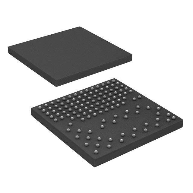
| 描述 | IC DAC 12BIT DUAL W/SPI 8MSOP数模转换器- DAC Dual 12-bit DAC |
| 产品分类 | |
| 品牌 | Microchip Technology |
| 产品手册 | |
| 产品图片 |
|
| rohs | 符合RoHS无铅 / 符合限制有害物质指令(RoHS)规范要求 |
| 产品系列 | 数据转换器IC,数模转换器- DAC,Microchip Technology MCP4822-E/MS- |
| 数据手册 | http://www.microchip.com/mymicrochip/filehandler.aspx?ddocname=en547855http://www.microchip.com/mymicrochip/filehandler.aspx?ddocname=en023833 |
| 产品型号 | MCP4822-E/MS |
| 产品目录页面 | |
| 产品种类 | 数模转换器- DAC |
| 位数 | 12 |
| 供应商器件封装 | 8-MSOP |
| 其它名称 | MCP4822EMS |
| 分辨率 | 12 bit |
| 包装 | 管件 |
| 商标 | Microchip Technology |
| 安装类型 | 表面贴装 |
| 安装风格 | SMD/SMT |
| 封装 | Tube |
| 封装/外壳 | 8-TSSOP,8-MSOP(0.118",3.00mm 宽) |
| 封装/箱体 | MSOP |
| 工作温度 | -40°C ~ 125°C |
| 工厂包装数量 | 100 |
| 建立时间 | 4.5µs |
| 接口类型 | SPI, Serial (3-Wire, Microwire) |
| 数据接口 | SPI |
| 最大工作温度 | + 125 C |
| 最小工作温度 | - 40 C |
| 标准包装 | 100 |
| 电压参考 | Internal |
| 电压源 | 单电源 |
| 电源电压-最大 | 5.5 V |
| 电源电压-最小 | 2.7 V |
| 积分非线性 | +/- 12 LSB |
| 稳定时间 | 4.5 us |
| 结构 | Resistor-String |
| 转换器数 | 2 |
| 转换器数量 | 2 |
| 输出数和类型 | 2 电压,单极2 电压,双极 |
| 输出类型 | Voltage |
| 采样率(每秒) | * |


- 商务部:美国ITC正式对集成电路等产品启动337调查
- 曝三星4nm工艺存在良率问题 高通将骁龙8 Gen1或转产台积电
- 太阳诱电将投资9.5亿元在常州建新厂生产MLCC 预计2023年完工
- 英特尔发布欧洲新工厂建设计划 深化IDM 2.0 战略
- 台积电先进制程称霸业界 有大客户加持明年业绩稳了
- 达到5530亿美元!SIA预计今年全球半导体销售额将创下新高
- 英特尔拟将自动驾驶子公司Mobileye上市 估值或超500亿美元
- 三星加码芯片和SET,合并消费电子和移动部门,撤换高东真等 CEO
- 三星电子宣布重大人事变动 还合并消费电子和移动部门
- 海关总署:前11个月进口集成电路产品价值2.52万亿元 增长14.8%


PDF Datasheet 数据手册内容提取
MCP4821/MCP4822 12-Bit DACs with Internal V and SPI™ Interface REF Features Description • 12-Bit Resolution The Microchip Technology Inc. MCP482X devices are (cid:129) ±0.2LSb DNL (typ.) 2.7V–5.5V, low-power, low DNL, 12-bit Digital-to-Analog Converters (DACs) with internal band gap voltage (cid:129) ±2LSb INL (typ.) reference, optional 2x-buffered output and Serial (cid:129) Single or Dual Channel Peripheral Interface (SPI™). (cid:129) Rail-to-Rail Output The MCP482X family of DACs provide high accuracy (cid:129) SPI™ Interface with 20MHz Clock Support and low noise performance for industrial applications (cid:129) Simultaneous Latching of the Dual DACs where calibration or compensation of signals (such as with LDAC pin temperature, pressure and humidity) are required. (cid:129) Fast Settling Time of 4.5µs The MCP482X devices are available in the extended (cid:129) Selectable Unity or 2x Gain Output temperature range and PDIP, SOIC and MSOP (cid:129) 2.048V Internal Band Gap Voltage Reference packages. (cid:129) 50ppm/°C V Temperature Coefficient The MCP482X devices utilize a resistive string REF architecture, with its inherent advantages of low DNL (cid:129) 2.7V to 5.5V Single-Supply Operation error, low ratio metric temperature coefficient and fast (cid:129) Extended Temperature Range:-40°C to +125°C settling time. These devices are specified over the extended temperature range. The MCP482X family Applications includes double-buffered registers, allowing simulta- neous updates using the LDAC pin. These devices also (cid:129) Set Point or Offset Trimming incorporate a Power-On Reset (POR) circuit to ensure (cid:129) Sensor Calibration reliable power-up. (cid:129) Precision Selectable Voltage Reference Package Types (cid:129) Portable Instrumentation (Battery-Powered) (cid:129) Calibration of Optical Communication Devices 8-Pin PDIP, SOIC, MSOP Block Diagram VDD 1 1 8 VOUTA 2 CS SDI SCK LDAC CS 2 8 7 AVSS 4 SCK 3 P 6 SHDN C VDD SDI 4 M 5 LDAC Power-on Interface Logic Reset AVSS 8-Pin PDIP, SOIC, MSOP Input Input Register A Register B VDD 1 2 8 VOUTA RDeAgCisAte r RDeAgCisBte r 2V.0R4E8FV SCCSK 23 P482 76 AVVOSUSTB C SDI 4 M 5 LDAC String String DACA DACB Gain Gain Logic Output Logic Op Amps Output Logic VOUTA SHDN VOUTB © 2005 Microchip Technology Inc. DS21953A-page 1
MCP4821/MCP4822 1.0 ELECTRICAL † Notice: Stresses above those listed under “Maximum Ratings” may cause permanent damage to the device. This is CHARACTERISTICS a stress rating only and functional operation of the device at those or any other conditions above those indicated in the Absolute Maximum Ratings † operational listings of this specification is not implied. Exposure to maximum rating conditions for extended periods VDD............................................................................................................. 6.5V may affect device reliability. All inputs and outputs ...................AV – 0.3V to V + 0.3V SS DD Current at Input Pins ....................................................±2mA Current at Supply Pins ...............................................±50mA Current at Output Pins ...............................................±25mA Storage temperature.....................................-65°C to +150°C Ambient temp. with power applied................-55°C to +125°C ESD protection on all pins ...........≥ 4kV (HBM), ≥ 400V (MM) Maximum Junction Temperature (T )..........................+150°C J 5V AC/DC CHARACTERISTICS Electrical Specifications: Unless otherwise indicated, V = 5V, AV = 0V, V = 2.048V, output buffer gain (G) = 2x, DD SS REF R = 5kΩ to GND, C = 100pF, T = -40 to +85°C. Typical values at +25°C. L L A Parameters Sym Min Typ Max Units Conditions Power Requirements Input Voltage V 2.7 — 5.5 DD Input Current - MCP4821 I — 330 400 µA Digital inputs grounded, Output DD Input Current - MCP4822 — 415 750 unloaded, code = 0x000 Hardware Shutdown Current I — 0.3 2 µA SHDN Software Shutdown Current I — 3.3 6 µA SHDN_SW Power-on-Reset Threshold V — 2.0 — V POR DC Accuracy Resolution n 12 — — Bits INL Error INL -12 2 12 LSb DNL (Note 1) DNL -0.75 ±0.2 +0.75 LSb Device is monotonic Offset Error V -1 ±0.02 1 % of FSR Code = 0x000h OS Offset Error Temperature V /°C — 0.16 — ppm/°C -45°C to 25°C OS Coefficient — -0.44 — ppm/°C +25°C to 85°C Gain Error g -2 -0.10 2 % of FSR Code 0xFFFh, not including offset E error Δ Gain Error Temperature G/°C — -3 — ppm/°C Coefficient Internal Voltage Reference (V ) REF Nominal Reference Voltage V 2.008 2.048 2.088 V V when G = 1x and REF OUTA Code = 0xFFFh Δ Temperature Coefficient V /°C — 125 325 ppm/°C -40°C to 0°C REF (Note 1) — 0.25 0.65 LSb/°C -40°C to 0°C — 45 160 ppm/°C 0°C to +85°C — 0.09 0.32 LSb/°C 0°C to +85°C Output Noise (V Noise) E — 290 — µV Code = 0xFFFh, G = 1 REF NREF p-p (0.1-10Hz) Output Noise Density e — 1.2 — µV/√Hz Code = 0xFFFh, G = 1 NREF (1kHz) e — 1.0 — µV/√Hz Code = 0xFFFh, G = 1 NREF (10kHz) 1/f Corner Frequency f — 400 — Hz CORNER Note 1: By design, not production tested. 2: Too small to quantify. DS21953A-page 2 © 2005 Microchip Technology Inc.
MCP4821/MCP4822 5V AC/DC CHARACTERISTICS (CONTINUED) Electrical Specifications: Unless otherwise indicated, V = 5V, AV = 0V, V = 2.048V, output buffer gain (G) = 2x, DD SS REF R = 5kΩ to GND, C = 100pF, T = -40 to +85°C. Typical values at +25°C. L L A Parameters Sym Min Typ Max Units Conditions Output Amplifier Output Swing V — 0.010 to — Accuracy is better than 1 LSb for OUT V – 0.040 V = 10mV to (V – 40mV) DD OUT DD Phase Margin PM — 66 — ° Slew Rate SR — 0.55 — V/µs Short Circuit Current I — 15 24 mA SC Settling Time t — 4.5 — µs Within 1/2 LSb of final value from SETTLING 1/4 to 3/4 full-scale range Dynamic Performance DAC-to-DAC Crosstalk — <10 — nV-s Note2 Major Code Transition Glitch — 45 — nV-s 1 LSb change around major carry (0111...1111 to 1000...0000) Digital Feedthrough — <10 — nV-s Note2 Analog Crosstalk — <10 — nV-s Note2 Note 1: By design, not production tested. 2: Too small to quantify. 3V AC/DC CHARACTERISTICS Electrical Specifications: Unless otherwise indicated, V = 3V, AV = 0V, V = 2.048V external, output buffer gain (G) = 1x, DD SS REF R = 5kΩ to GND, C = 100pF, T = -40 to +85°C. Typical values at 25°C L L A Parameters Sym Min Typ Max Units Conditions Power Requirements Input Voltage V 2.7 — 5.5 DD Input Current - MCP4821 I — 300 400 µA Digital inputs grounded, Output DD Input Current - MCP4822 — 415 750 unloaded, code = 0x000 Hardware Shutdown Current I — 0.25 2 µA SHDN Software Shutdown Current I — 2 6 µA SHDN_SW Power-On Reset threshold V — 2.0 — V POR DC Accuracy Resolution n 12 — — Bits INL Error INL -12 ±3 12 LSb DNL (Note 1) DNL -0.75 ±0.3 0.75 LSb Device is monotonic Offset Error V -1 ±0.02 1 % of FSR Code 0x000h OS Offset Error Temperature V /°C — 0.5 — ppm/°C -45°C to +25°C OS Coefficient — -0.77 — ppm/°C +25°C to +85°C Gain Error g -2 -0.15 2 % of FSR Code 0xFFFh, not including off- E set error Δ Gain Error Temperature G/°C — -3 — ppm/°C Coefficient Note 1: By design, not production tested. 2: Too small to quantify. © 2005 Microchip Technology Inc. DS21953A-page 3
MCP4821/MCP4822 3V AC/DC CHARACTERISTICS (CONTINUED) Electrical Specifications: Unless otherwise indicated, V = 3V, AV = 0V, V = 2.048V external, output buffer gain (G) = 1x, DD SS REF R = 5kΩ to GND, C = 100pF, T = -40 to +85°C. Typical values at 25°C L L A Parameters Sym Min Typ Max Units Conditions Internal Voltage Reference (V ) REF Nominal Reference Voltage V 2.008 2.048 2.088 V V when G = 1x and REF OUTA Code = 0xFFFh Δ Temperature Coefficient V /°C — 125 325 ppm/°C -40°C to 0°C REF (Note 1) — 0.25 0.65 LSb/°C -40°C to 0°C — 45 160 ppm/°C 0°C to +85°C — 0.09 0.32 LSb/°C 0°C to +85°C Output Noise (V Noise) E — 290 — µV Code = 0xFFFh, G = 1 REF NREF p-p (0.1-10Hz) Output Noise Density e — 1.2 — µV/√Hz Code = 0xFFFh, G = 1 NREF (1kHz) e — 1.0 — µV/√Hz Code = 0xFFFh, G = 1 NREF (10kHz) 1/f Corner Frequency f — 400 — Hz CORNER Output Amplifier Output Swing V — 0.010 to — Accuracy is better than 1LSb for OUT V – 0.040 V = 10mV to (V – 40mV) DD OUT DD Phase Margin PM — 66 — ° Slew Rate SR — 0.55 — V/µs Short Circuit Current I — 14 24 mA SC Settling Time t — 4.5 — µs Within 1/2 LSb of final value from SETTLING 1/4 to 3/4 full-scale range Dynamic Performance DAC-to-DAC Crosstalk — <10 — nV-s Note2 Major Code Transition Glitch — 45 — nV-s 1 LSb change around major carry (0111...1111 to 1000...0000) Digital Feedthrough — <10 — nV-s Note2 Analog Crosstalk — <10 — nV-s Note2 Note 1: By design, not production tested. 2: Too small to quantify. 5V EXTENDED TEMPERATURE SPECIFICATIONS Electrical Specifications: Unless otherwise indicated, V = 5V, AV = 0V, V = 2.048V, output buffer gain (G) = 2x, DD SS REF R = 5kΩ to GND, C = 100pF. Typical values at +125°C by characterization or simulation. L L Parameters Sym Min Typ Max Units Conditions Power Requirements Input Voltage V 2.7 — 5.5 DD Input Current - MCP4821 I — 350 — µA Digital inputs grounded, Output DD Input Current - MCP4822 — 440 unloaded, code = 0x000 Hardware Shutdown Current I — 1.5 — µA SHDN Software Shutdown Current I — 5 — µA SHDN_SW Power-On Reset threshold V — 1.85 — V POR DC Accuracy Resolution n 12 — — Bits INL Error INL — ±4 — LSb Note 1: By design, not production tested. 2: Too small to quantify. DS21953A-page 4 © 2005 Microchip Technology Inc.
MCP4821/MCP4822 5V EXTENDED TEMPERATURE SPECIFICATIONS (CONTINUED) Electrical Specifications: Unless otherwise indicated, V = 5V, AV = 0V, V = 2.048V, output buffer gain (G) = 2x, DD SS REF R = 5kΩ to GND, C = 100pF. Typical values at +125°C by characterization or simulation. L L Parameters Sym Min Typ Max Units Conditions DNL (Note 1) DNL — ±0.25 — LSb Device is monotonic Offset Error V — ±0.02 — % of FSR Code 0x000h OS Offset Error Temperature V /°C — -5 — ppm/°C +25°C to +125°C OS Coefficient Gain Error g — -0.10 — % of FSR Code 0xFFFh, not including offset E error Δ Gain Error Temperature G/°C — -3 — ppm/°C Coefficient Internal Voltage Reference (V ) REF Nominal Reference Voltage V — 2.048 — V V when G = 1x and REF OUTA Code = 0xFFFh Δ Temperature Coefficient V /°C — 125 — ppm/°C -40°C to 0°C REF (Note 1) — 0.25 — LSb/°C -40°C to 0°C — 45 — ppm/°C 0°C to +85°C — 0.09 — LSb/°C 0°C to +85°C Output Noise (V Noise) E — 290 — µV Code = 0xFFFh, G = 1 REF NREF p-p (0.1 - 10Hz) Output Noise Density e — 1.2 — µV/√Hz Code = 0xFFFh, G = 1 NREF (1kHz) e — 1.0 — µV/√Hz Code = 0xFFFh, G = 1 NREF (10kHz) 1/f Corner Frequency f — 400 — Hz CORNER Output Amplifier Output Swing V — 0.010 to — Accuracy is better than 1LSb for OUT V – 0.040 V = 10mV to (V – 40mV) DD OUT DD Phase Margin PM — 66 — ° Slew Rate SR — 0.55 — V/µs Short Circuit Current I — 17 — mA SC Settling Time t — 4.5 — µs Within 1/2 LSb of final value from SETTLING 1/4 to 3/4 full-scale range Dynamic Performance DAC-to-DAC Crosstalk — <10 — nV-s Note2 Major Code Transition Glitch — 45 — nV-s 1 LSb change around major carry (0111...1111 to 1000...0000) Digital Feedthrough — <10 — nV-s Note2 Analog Crosstalk — <10 — nV-s Note2 Note 1: By design, not production tested. 2: Too small to quantify. © 2005 Microchip Technology Inc. DS21953A-page 5
MCP4821/MCP4822 AC CHARACTERISTICS (SPI™ TIMING SPECIFICATIONS) Electrical Specifications: Unless otherwise indicated, V = 2.7V – 5.5V, T = -40 to +125°C. DD A Typical values are at +25°C. Parameters Sym Min Typ Max Units Conditions Schmitt Trigger High-Level V 0.7V — — V IH DD Input Voltage (All digital input pins) Schmitt Trigger Low-Level V — — 0.2V V IL DD Input Voltage (All digital input pins) Hysteresis of Schmitt Trigger V — 0.05V — HYS DD Inputs Input Leakage Current I -1 — 1 μA SHDN = LDAC = CS = SDI = LEAKAGE SCK + V = V or AV REF DD SS Digital Pin Capacitance C , — 10 — pF V = 5.0V, T = +25°C, IN DD A (All inputs/outputs) C f = 1MHz (Note1) OUT CLK Clock Frequency F — — 20 MHz T = +25°C (Note1) CLK A Clock High Time t 15 — — ns Note1 HI Clock Low Time t 15 — — ns Note1 LO CS Fall to First Rising CLK t 40 — — ns Applies only when CS falls with CSSR Edge CLK high. (Note1) Data Input Setup Time t 15 — — ns Note1 SU Data Input Hold Time t 10 — — ns Note1 HD SCK Rise to CS Rise Hold t 15 — — ns Note1 CHS Time CS High Time t 15 — — ns Note1 CSH LDAC Pulse Width t 100 — — ns Note1 LD LDAC Setup Time t 40 — — ns Note1 LS SCK Idle Time before CS Fall t 40 — — ns Note1 IDLE Note 1: By design and characterization, not production tested. t CSH CS t IDLE tCSSR tHI tLO tCHS Mode 1,1 SCKMode 0,0 t t SU HD SI MSb in LSb in LDAC tLS tLD FIGURE 1-1: SPI™ Input Timing. DS21953A-page 6 © 2005 Microchip Technology Inc.
MCP4821/MCP4822 TEMPERATURE CHARACTERISTICS Electrical Specifications: Unless otherwise indicated, V =+2.7V to +5.5V, AV =GND. DD SS Parameters Sym Min Typ Max Units Conditions Temperature Ranges Specified Temperature Range T -40 — +125 °C A Operating Temperature Range T -40 — +125 °C Note1 A Storage Temperature Range T -65 — +150 °C A Thermal Package Resistances Thermal Resistance, 8L-PDIP θ — 85 — °C/W JA Thermal Resistance, 8L-SOIC θ — 163 — °C/W JA Thermal Resistance, 8L-MSOP θ — 206 — °C/W JA Note 1: The MCP482X family of DACs operate over this extended temperature range, but with reduced performance. Operation in this range must not cause T to exceed the Maximum Junction Temperature of J +150°C. © 2005 Microchip Technology Inc. DS21953A-page 7
MCP4821/MCP4822 2.0 TYPICAL PERFORMANCE CURVES Note: The graphs and tables provided following this note are a statistical summary based on a limited number of samples and are provided for informational purposes only. The performance characteristics listed herein are not tested or guaranteed. In some graphs or tables, the data presented may be outside the specified operating range (e.g., outside specified power supply range) and therefore outside the warranted range. Note: Unless otherwise indicated, T = +25°C, V = 5V, AV = 0V, V = 2.048V, Gain = 2, R = 5kΩ, C = 100pF. A DD SS REF L L 0.3 5 Ambient Temperature 4 0.2 125C 85 25 3 NL (LSB) 0.10 L (LSB) -0121 D -0.1 N I -2 -0.2 -3 -4 -0.3 -5 0 1024 2048 3072 4096 0 1024 2048 3072 4096 Code (Decimal) Code (Decimal) FIGURE 2-1: DNL vs. Code. FIGURE 2-4: INL vs. Code and Ambient Temperature. 0.2 2.5 2 0.1 B) S SB) L (L 1.5 L 0 N DNL (-0.1 bsolute I 0.51 A -0.2 0 0 1024 2048 3072 4096 -40 -20 0 20 40 60 80 100 120 Code (Decimal) 125C 85C 25C Ambient Temperature (ºC) FIGURE 2-2: DNL vs. Code and Ambient FIGURE 2-5: Absolute INL vs. Ambient Temperature. Temperature. 0.0766 2 0.0764 SB) 0.0762 0 L e DNL ( 00.0.077568 L (LSB) -2 solut 00..00775546 IN -4 b A 0.0752 0.075 -6 -40 -20 0 20 40 60 80 100 120 0 1024 2048 3072 4096 Ambient Temperature (ºC) Code (Decimal) FIGURE 2-3: Absolute DNL vs. Ambient FIGURE 2-6: INL vs. Code. Temperature. Note: Single device graph for illustration of 64 code effect. DS21953A-page 8 © 2005 Microchip Technology Inc.
MCP4821/MCP4822 Note: Unless otherwise indicated, T = +25°C, V = 5V, AV = 0V, V = 2.048V, Gain = 2, R = 5kΩ, C = 100pF. A DD SS REF L L 2.050 1.E1-0004 y 2.049 sit n V) 2.048 De (UT 2.047 ge 1.E-1005 ull Scale VO 2222....000044443456 VVVDDDDDD::: 432VV.7V Noise Volta(μV/Hz)1(cid:151).E-016 F 2.042 ut p 2.041 ut 2.040 O1.E0-0.17 -40 -20 0 20 40 60 80 100 120 1E0.-11 1E1+0 1E1+01 11E0+02 1E1+k3 11E0+k4 11E00+k5 Ambient Temperature (°C) Frequency (Hz) FIGURE 2-7: Full-Scale V w/G = 1 FIGURE 2-9: Output Noise Voltage OUTA (V ) vs. Ambient Temperature and V . Density (V Noise Density w/G = 1) vs. REF DD REF Frequency. 4.100 1.E1-00.02 Full Scale V (V)OUT 44444.....000008889904826 VVDDDD:: 55.V5V put Noise Voltage (mV)11..EE01--..10000430 EEnnii ((iinn VVRP-MPS)) ut O 4.076 Maximum Measurement Time = 10s 1.E0-.0015 -40 -20 0 20 40 60 80 100 120 11E0+02 1E1k+3 11E0+k4 11E00+k5 11EM+6 Ambient Temperature (°C) Bandwidth (Hz) FIGURE 2-8: Full-Scale V w/G = 2 FIGURE 2-10: Output Noise Voltage (V OUTA REF (2V ) vs.Ambient Temperature and V . Noise Voltage w/G = 1) vs. Bandwidth. REF DD © 2005 Microchip Technology Inc. DS21953A-page 9
MCP4821/MCP4822 Note: Unless otherwise indicated, T = +25°C, V = 5V, AV = 0V, V = 2.048V, Gain = 2, R = 5kΩ, C = 100pF. A DD SS REF L L 340 600 5.5V 320 5.0V 5.5V 4.0V 550 5.0V 300 3.0V 4.0V 2.7V 3.0V A)280 VDD A)500 V2.D7DV (μD260 (μD450 ID240 ID 400 220 350 200 180 300 -40 -20 0 20 40 60 80 100 120 -40 -20 0 20 40 60 80 100 120 Ambient Temperature (°C) Ambient Temperature (ºC) FIGURE 2-11: MCP4821 I vs. Ambient FIGURE 2-14: MCP4822 I vs. Ambient DD DD Temperature and V . Temperature and V . DD DD 20 25 18 16 20 Occurrence11168024 Occurrence1105 4 5 2 0 0 5 0 5 0 5 0 5 0 5 0 5 0 0 6 7 7 8 8 9 9 0 0 1 1 2 2 0 5 0 5 0 5 0 5 0 5 0 5 0 2 2 2 2 2 2 2 3 3 3 3 3 3 8 8 9 9 0 0 1 1 2 2 3 3 4 > 3 3 3 3 4 4 4 4 4 4 4 4 4 I (μA) I (μA) DD DD FIGURE 2-12: MCP4821 I Histogram FIGURE 2-15: MCP4822 I Histogram DD DD (V = 2.7V). (V = 2.7V). DD DD 18 22 16 20 18 14 16 Occurrence116802 Occurrence 1118024 6 4 4 2 2 0 0 5 0 5 0 5 0 5 0 5 0 5 0 5 0 0 5 0 5 0 5 0 5 0 5 0 5 8 9 9 0 0 1 1 2 2 3 3 4 4 5 5 8 9 9 0 0 1 1 2 2 3 3 2 2 2 3 3 3 3 3 3 3 3 3 3 3 3 3 3 3 4 4 4 4 4 4 4 4 IDD (μA) > IDD (μA) FIGURE 2-13: MCP4821 I Histogram FIGURE 2-16: MCP4822 I Histogram DD DD (V = 5.0V). (V = 5.0V). DD DD DS21953A-page 10 © 2005 Microchip Technology Inc.
MCP4821/MCP4822 Note: Unless otherwise indicated, T = +25°C, V = 5V, AV = 0V, V = 2.048V, Gain = 2, R = 5kΩ, C = 100pF. A DD SS REF L L 0.7 5.5V -0.05 0.6 5.0V -0.1 4.0V VDD (μA)SHDN000...345 V32..D07DVV n Error (%) --00--..0021..5532 54532.....50007VVVVV I ai -0.35 0.2 G -0.4 0.1 -0.45 0 -0.5 -40 -20 0 20 40 60 80 100 120 -40 -20 0 20 40 60 80 100 120 Ambient Temperature (ºC) Ambient Temperature (ºC) FIGURE 2-17: Hardware Shutdown Current FIGURE 2-20: Gain Error vs. Ambient vs. Ambient Temperature and V . Temperature and V . DD DD 4 5.5V 4 VDD 3.5 5.0V 5.5V 3.5 V) 5.0V A) 3 4.0V d ( 3 μ ol I (SHDN_SW2.52 V32D..07DVV Hi ThreshN 2.52 43..00VV 1.5 VI 1.5 2.7V 1 1 -40 -20 0 20 40 60 80 100 120 -40 -20 0 20 40 60 80 100 120 Ambient Temperature (ºC) Ambient Temperature (ºC) FIGURE 2-18: Software Shutdown Current FIGURE 2-21: V High Threshold vs. IN vs. Ambient Temperature and V . Ambient Temperature and V . DD DD 0.11 1.6 VDD or (%) 00..0079 shold (V) 111...345 55..50VV Offset Err 000...000135 5V.D5DV Low Thre 11..12 4.0V -0.01 5.0V V IN 1 3.0V 4.0V 0.9 3.0V 2.7V -0.03 2.7V 0.8 -40 -20 0 20 40 60 80 100 120 -40 -20 0 20 40 60 80 100 120 Ambient Temperature (ºC) Ambient Temperature (ºC) FIGURE 2-19: Offset Error vs. Ambient FIGURE 2-22: V Low Threshold vs. IN Temperature and V . Ambient Temperature and V . DD DD © 2005 Microchip Technology Inc. DS21953A-page 11
MCP4821/MCP4822 Note: Unless otherwise indicated, T = +25°C, V = 5V, AV = 0V, V = 2.048V, Gain = 2, R = 5kΩ, C = 100pF. A DD SS REF L L 2.5 16 2.25 VDD 55..50VV steresis (V) 11..127.5552 545...500VVV (mA)ORTED 111345 V432...D007DVVV y H _ HSPI 0.751 32..07VV UT_HI_S 12 VIN 0.5 IO 11 0.25 0 10 -40 -20 0 20 40 60 80 100 120 -40 -20 0 20 40 60 80 100 120 Ambient Temperature (ºC) Ambient Temperature (ºC) FIGURE 2-23: Input Hysteresis vs. Ambient FIGURE 2-26: I High Short vs. Ambient OUT Temperature and V . Temperature and V . DD DD 0.035 6.0 4.0V 0.033 5.0 Y)(V) 00..002391 4.0 VREF = 4.096V mit (V-DD 00..002257 3.0V V (V)OUT 3.0 Output Shorted to VDD Li 0.023 2.7V 2.0 V OUT_HI 000...000112791 VDD 1.0 Output Shorted to VSS 0.0 0.015 0 2 4 6 8 10 12 14 16 -40 -20 0 20 40 60 80 100 120 I (mA) Ambient Temperature (ºC) OUT FIGURE 2-24: VOUT High Limit vs. Ambient FIGURE 2-27: IOUT vs. VOUT. Gain = 2. Temperature and V . DD 0.0028 VDD V) 0.0026 )(S 0.0024 5.5V S AV 0.0022 5.0V Y- 0.0020 mit ( 0.0018 4.0V LiW 0.0016 32..07VV OUT_LO 00..00001124 V 0.0010 -40 -20 0 20 40 60 80 100 120 Ambient Temperature (ºC) FIGURE 2-25: V Low Limit vs. Ambient OUT Temperature and V . DD DS21953A-page 12 © 2005 Microchip Technology Inc.
MCP4821/MCP4822 Note: Unless otherwise indicated, T = +25°C, V = 5V, AV = 0V, V = 2.048V, Gain = 2, R = 5kΩ, C = 100pF. A DD SS REF L L V OUT V OUT SCK LDAC LDAC Time (1µs/div) Time (1µs/div) FIGURE 2-28: V Rise Time 100%. FIGURE 2-31: V Rise Time 25% - 75%. OUT OUT V OUT V OUT SCK SCK LDAC LDAC Time (1µs/div) Time (1µs/div) FIGURE 2-29: V Fall Time. FIGURE 2-32: V Rise Time Exit OUT OUT Shutdown. ) B d ( n o V ti OUT c e SCK ej R e pl p Ri LDAC Time (1µs/div) Frequency (Hz) FIGURE 2-30: V Rise Time 50%. FIGURE 2-33: PSRR vs. Frequency. OUT © 2005 Microchip Technology Inc. DS21953A-page 13
MCP4821/MCP4822 3.0 PIN DESCRIPTIONS The descriptions of the pins are listed in Table3-1. TABLE 3-1: PIN FUNCTION TABLE MCP4821 MCP4822 Symbol Function Pin No. Pin No. 1 1 V Positive Power Supply Input (2.7V to 5.5V) DD 2 2 CS Chip Select Input 3 3 SCK Serial Clock Input 4 4 SDI Serial Data Input 5 5 LDAC Synchronization input used to transfer DAC settings from serial latches to output latches 6 — SHDN Hardware Shutdown Input — 6 V DAC Output OUTB B 7 7 AV Analog Ground SS 8 8 V DAC Output OUTA A 3.1 Positive Power Supply Input (V ) 3.6 Hardware Shutdown Input (SHDN) DD V is the positive power supply input. The input power SHDN is the hardware shutdown input that requires an DD supply is relative to AV and can range from 2.7V to active-low input signal to configure the DACs in their SS 5.5V. A decoupling capacitor on V is recommended low-power Standby mode. DD to achieve maximum performance. 3.7 DAC Outputs (V , V ) x OUTA OUTB 3.2 Chip Select (CS) V and V are DAC outputs. The DAC output OUTA OUTB CS is the chip select input, which requires an active-low amplifier drives these pins with a range of AV to V . SS DD signal to enable serial clock and data functions. 3.8 Analog Ground (AV ) SS 3.3 Serial Clock Input (SCK) AV is the analog ground pin. SS SCK is the SPI compatible serial clock input. 3.4 Serial Data Input (SDI) SDI is the SPI compatible serial data input. 3.5 Latch DAC Input (LDAC) LDAC (the latch DAC synchronization input) transfers the input latch registers to the DAC registers (output latches) when low. Can also be tied low if transfer on the rising edge of CS is desired. DS21953A-page 14 © 2005 Microchip Technology Inc.
MCP4821/MCP4822 4.0 GENERAL OVERVIEW The MCP482X devices are voltage-output string DACs. INL < 0 These devices include rail-to-rail output amplifiers, 111 internal voltage reference, shutdown and reset-man- Actual agement circuitry. Serial communication conforms to 110 Transfer Function the SPI protocol. The MCP482X devices operate from 101 2.7V to 5.5V supplies. The coding of these devices is straight binary, with the Digital 100 ideal output voltage given by Equation4-1, where G is Input the selected gain (1x or 2x), DN represents the digital Code 011 Ideal Transfer input value and n represents the number of bits of Function resolution (n = 12). 010 EQUATION 4-1: LSb SIZE 001 2.048V⋅G⋅D 000 V = ------------------------------------N-- OUT n INL < 0 2 DAC Output 1LSb is the ideal voltage difference between two successive codes. Table4-1 illustrates how to calculate FIGURE 4-1: INL Accuracy. LSb. 4.0.2 DNL ACCURACY T ABLE 4-1: LSb SIZES DNL error is the measure of variations in code widths Device Gain LSb Size from the ideal code width. A DNL error of zero would MCP482X 1x 2.048V/4096 imply that every code is exactly 1LSb wide. MCP482X 2x 4.096V/4096 4.0.1 INL ACCURACY 111 Actual INL error for these devices is the maximum deviation Transfer between an actual code transition point and its corre- 110 Function sponding ideal transition point once offset and gain 101 errors have been removed. These endpoints are from 0x000 to 0xFFF. Refer to Figure4-1. Digital 100 Input Ideal Transfer Positive INL represents transition(s) later than ideal. Code 011 Function Negative INL represents transition(s) earlier than ideal. 010 001 Wide Code > 1 LSb 000 Narrow Code < 1 LSb DAC Output FIGURE 4-2: DNL Accuracy. 4.0.3 OFFSET ERROR Offset error is the deviation from zero voltage output when the digital input code is zero. 4.0.4 GAIN ERROR Gain error is the deviation from the ideal output, V – 1LSb, excluding the effects of offset error. REF © 2005 Microchip Technology Inc. DS21953A-page 15
MCP4821/MCP4822 4.1 Circuit Descriptions 4.1.1 OUTPUT AMPLIFIERS 5V The DACs’ outputs are buffered with a low-power, es VPOR g pofrfesceits ivoonlt aCgMe OaSnd a lmowp lnifioeirs.e T. hTihs ea omuptplifuiet rs tpargoev iedneasb lloews olta VDD - VPOR V the device to operate with output voltages close to the y pl Transient Duration power supply rails. Refer to Section1.0 “Electrical p u Characteristics” for range and load conditions. S In addition to resistive load-driving capability, the ampli- Time fier will also drive high capacitive loads without oscilla- 10 tion. The amplifiers’ strong outputs allow VOUT to be TA = +25°C used as a programmable voltage reference in a µs) 8 system. n ( o 4.1.1.1 Programmable Gain Block ati 6 r u The rail-to-rail output amplifier has configurable gain, D allowing optimal full-scale outputs for differing voltage ent 4 Transients above the curve reference inputs. The output amplifier gain has two nsi 2 will cause a reset a selections, a gain of 1V/V (GA = 1) or a gain of 2V/V Tr Transients below the curve (GA = 0). 0 will NOT cause a reset 1 2 3 4 5 The output range is ideally 0.000V to 4095/4096 * V – V (V) DD POR 2.048V when G = 1, and 0.000 to 4095/4096 * 4.096V when G=2. The default value for this bit is a gain of 2, FIGURE 4-3: Typical Transient Response. yielding an ideal full-scale output of 0.000V to 4.096V due to the internal 2.048V V . Note that the near rail- 4.1.4 SHUTDOWN MODE REF to-rail CMOS output buffer’s ability to approach AVSS Shutdown mode can be entered by using either hard- and VDD establish practical range limitations. The ware or software commands. The hardware pin output swing specification in Section1.0 “Electrical (SHDN) is only available on the MCP4821. During Characteristics” defines the range for a given load Shutdown mode, the supply current is isolated from condition. most of the internal circuitry. The serial interface remains active, thus allowing a Write command to 4.1.2 VOLTAGE REFERENCE bring the device out of Shutdown mode. When the out- The MCP482X devices utilize internal 2.048V voltage put amplifiers are shut down, the feedback resistance reference. The voltage reference has low temperature (typically 500kΩ) produces a high-impedance path to coefficient and low noise characteristics. Refer to AVSS. The device will remain in Shutdown mode until Section1.0 “Electrical Characteristics” for the the SHDN pin is brought high and a write command voltage reference specifications. with SD = 1 is latched into the device. When a DAC is changed from Shutdown to Active mode, the output 4.1.3 POWER-ON RESET CIRCUIT settling time takes < 10µs, but greater than the standard Active mode settling time (4.5µs). The Power-On Reset (POR) circuit ensures that the DACs power-up with SHDN = 0 (high-impedance). The devices will continue to have a high-impedance output until a valid Write command is performed to either of the DAC registers and the LDAC pin meets the input low threshold. If the power supply voltage is less than the POR threshold (V = 2.0V, typical), the DACs will be held POR in their reset state. They will remain in that state until V > V and a subsequent Write command is DD POR received. Figure4-3 shows a typical power supply transient pulse and the duration required to cause a reset to occur, as well as the relationship between the duration and trip voltage. A 0.1µF decoupling capacitor, mounted as close as possible to the V pin, provides DD additional transient immunity. DS21953A-page 16 © 2005 Microchip Technology Inc.
MCP4821/MCP4822 5.0 SERIAL INTERFACE 5.2 Write Command The write command is initiated by driving the CS pin 5.1 Overview low, followed by clocking the four configuration bits and the 12 data bits into the SDI pin on the rising edge of The MCP482X family is designed to interface directly SCK. The CS pin is then raised, causing the data to be with the SPI port, available on many microcontrollers, latched into the selected DAC’s input registers. The and supports Mode 0,0 and Mode 1,1. Commands and MCP482X devices utilize a double-buffered latch struc- data are sent to the device via the SDI pin, with data ture to allow both DAC ’s and DAC ’s outputs to be being clocked-in on the rising edge of SCK. The A B synchronized with the LDAC pin, if desired. Upon the communications are unidirectional and, thus, data LDAC pin achieving a low state, the values held in the cannot be read out of the MCP482X devices. The CS DAC’s input registers are transferred into the DACs’ pin must be held low for the duration of a write com- output registers. The outputs will transition to the value mand. The write command consists of 16 bits and is and held in the DAC register. used to configure the DAC’s control and data latches. X Register5-1 details the input registers used to All writes to the MCP482X devices are 16-bit words. configure and load the DAC and DAC registers. Any clocks past 16 will be ignored. The most signifi- A B Refer to Figure1-1 and the AC Electrical cant four bits are configuration bits. The remaining 12 Characteristics tables for detailed input and output tim- bits are data bits. No data can be transferred into the ing specifications for both Mode 0,0 and Mode 1,1 device with CS high. This transfer will only occur if 16 operation. clocks have been transferred into the device. If the rising edge of CS occurs prior, shifting of data into the input registers will be aborted. REGISTER 5-1: WRITE COMMAND REGISTER Upper Half: W-x W-x W-x W-0 W-x W-x W-x W-x A/B — GA SHDN D11 D10 D9 D8 bit 15 bit 8 Lower Half: W-x W-x W-x W-x W-x W-x W-x W-x D7 D6 D5 D4 D3 D2 D1 D0 bit 7 bit 0 bit 15 A/B: DAC or DAC Select bit A B 1 = Write to DAC B 0 = Write to DAC A bit 14 — Don’t Care bit 13 GA: Output Gain Select bit 1 = 1x (V = V * D/4096) OUT REF 0 = 2x (V = 2 * V * D/4096) OUT REF bit 12 SHDN: Output Power-down Control bit 1 = Output Power-down Control bit 0 = Output buffer disabled, Output is high-impedance bit 11-0 D11:D0: DAC Data bits 12-bit number “D” which sets the output value. Contains a value between 0 and 4095. Legend R = Readable bit W = Writable bit U = Unimplemented bit, read as ‘0’ -n = Value at POR 1 = bit is set 0 = bit is cleared x = bit is unknown © 2005 Microchip Technology Inc. DS21953A-page 17
MCP4821/MCP4822 CS 0 1 2 3 4 5 6 7 8 9 10 11 12 13 14 15 (Mode 1,1) SCK (Mode 0,0) config bits 12 data bits SDI A/B — GA SHDN D11 D10 D9 D8 D7 D6 D5 D4 D3 D2 D1 D0 LDAC V OUT FIGURE 5-1: Write Command. DS21953A-page 18 © 2005 Microchip Technology Inc.
MCP4821/MCP4822 6.0 TYPICAL APPLICATIONS 6.3 Output Noise Considerations The MCP482X devices are general purpose DACs The voltage noise density (in µV/√Hz) is illustrated in intended to be used in applications where a precision, Figure2-9. This noise appears at VOUTX, and is prima- low-power DAC with moderate bandwidth and internal rily a result of the internal reference voltage. Its 1/f voltage reference is required. corner (fCORNER) is approximately 400Hz. Applications generally suited for the MCP482X devices Figure2-10 illustrates the voltage noise (in mVRMS or include: mVP-P). A small bypass capacitor on VOUTX is an effective method to produce a single-pole Low-Pass (cid:129) Set Point or Offset Trimming Filter (LPF) that will reduce this noise. For instance, a (cid:129) Sensor Calibration bypass capacitor sized to produce a 1kHz LPF would (cid:129) Precision Selectable Voltage Reference result in an E of about 100 µV . This would be NREF RMS (cid:129) Portable Instrumentation (Battery-Powered) necessary when trying to achieve the low DNL (cid:129) Calibration of Optical Communication Devices performance (at G= 1) that the MCP482X devices are capable of. The tested range for stability is .001µF thru 6.1 Digital Interface 4.7 µF. The MCP482X devices utilize a 3-wire synchronous V V DD DD serial protocol to transfer the DACs’ setup and output values from the digital source. The serial protocol can be interfaced to SPI™ or Microwire peripherals com- 0.1µF0.1µF mon on many microcontroller units (MCUs), including Microchip’s PICmicro® MCUs and dsPIC® DSC family VDD CS of MCUs. In addition to the three serial connections V 1 (CS, SCK and SDI), the LDAC signal synchronizes OUTA X SDI wouhtepnu t tfhreom s ethriea ls eseritatil ningps uat rlea tclaht.c Fhiegdu reint6o- 1t hilelu sDtrAaCte’ss 0.1µF 1µF P482 oller the required connections. Note that LDAC is active-low. VOUTB MC ontr If desired, this input can be tied low to reduce the c o required connections from 4 to 3. Write commands will cr bcbleeoe clankt crtahriaesndes ddm.iriescstiloyn i nhtoa sth eb eoeuntp urte lcaetcivhe wd haennd a CvaSl idh 1a6s VOUTA 482X SDI AVSS SSDCOK ®cro Mi 1µF P mi C LDAC C 6.2 Power Supply Considerations VOUTB M CS0 PI The typical application will require a bypass capacitor in order to filter high-frequency noise. The noise can be induced onto the power supply's traces or as a result of changes on the DAC's output. The bypass capacitor AVSS AVSS helps to minimize the effect of these noise sources on signal integrity. Figure6-1 illustrates an appropriate FIGURE 6-1: Typical Connection bypass strategy. Diagram. In this example, the recommended bypass capacitor value is 0.1µF. This capacitor should be placed as 6.4 Layout Considerations close to the device power pin (V ) as possible (within DD 4mm). Inductively-coupled AC transients and digital switching noise can degrade the output signal integrity, The power source supplying these devices should be potentially masking the MCP482X family’s as clean as possible. If the application circuit has sep- performance. Careful board layout will minimize these arate digital and analog power supplies, AV and DD effects and increase the Signal-to-Noise Ratio (SNR). AV should reside on the analog plane. SS Bench testing has shown that a multi-layer board utilizing a low-inductance ground plane, isolated inputs, isolated outputs and proper decoupling are critical to achieving the performance that the MCP482X devices are capable of providing. Particularly harsh environments may require shielding of critical signals. Breadboards and wire-wrapped boards are not recommended if low noise is desired. © 2005 Microchip Technology Inc. DS21953A-page 19
MCP4821/MCP4822 6.5 Single-Supply Operation 6.5.1.1 Decreasing The Output Step Size The MCP482X devices are Rail-to-Rail (R-R) input and If the application is calibrating the threshold of a diode, output DACs designed to operate with a VDD range of transistor or resistor tied to AVSS, a threshold range of 2.7V to 5.5V. Its output amplifier is robust enough to 0.8V may be desired to provide 200µV resolution. Two drive common, small-signal loads directly, thus eliminat- common methods to achieve a 0.8V range is to either ing the cost and size of an external buffer for most reduce VREF to 0.82V (would require MCP492X device applications. and external voltage reference) or use a voltage divider on the DAC’s output. Typically, when using a low- 6.5.1 DC SET POINT OR CALIBRATION voltage VREF, the noise floor causes SNR error that is intolerable. The voltage divider method provides some A common application for a DAC with the MCP482X advantages when V needs to be very low or when family’s performance is a digitally-controlled set point REF the desired output voltage is not available. Using two and/or calibration of variable parameters, such as sen- resistors to scale the output range down to the precise sor offset or slope. 12-bit resolution provides 4096 out- desired level is a simple, low-cost method to achieve put steps. If G = 1 is selected, then the internal 2.048 very small step sizes. Example6-1 illustrates this V would produce 500µV of resolution. If G = 2 is REF concept. Note that the bypass capacitor on the output selected, the internal 2.048 V would produce 1mV REF of the voltage divider plays a critical function in of resolution. attenuating the output noise of the DAC and the induced noise from the environment. The MCP482X family’s low ±0.75 (max.) DNL performance is critical to meeting calibration accuracy in production. V DD V + CC R SENSE V DD Comparator VOUT R1 VTRIP MCP482X V – R 0.1uF CC 2 SPI™ 3 V = 2.048⋅G---D------ G = Gain select (1x or 2x) OUT 12 D = Digital value of DAC (0 – 4096) 2 ⎛ R2 ⎞ V = V ⎜--------------------⎟ trip OUT⎝R1+R2⎠ EXAMPLE 6-1: Set Point or Threshold Calibration. DS21953A-page 20 © 2005 Microchip Technology Inc.
MCP4821/MCP4822 6.5.1.2 Building a “Window” DAC creating a “window” around the threshold has several advantages. One simple method to create this When calibrating a set point or threshold of a sensor, “window” is to use a voltage divider network with a pull- rarely does the sensor utilize the entire output range of up and pull-down resistor. Example6-2 and the DAC. If the LSb size is adequate to meet the appli- Example6-4 illustrates this concept. cation’s accuracy needs, the resolution is sacrificed without consequences. If greater accuracy is needed, The MCP482X family’s low ±0.75 (max.) DNL then the output range will need to be reduced to performance is critical to meet calibration accuracy in increase the resolution around the desired threshold. If production. the threshold is not near V , 2V or AV , then REF REF SS V VCC+ RSENSE CC+ V DD R3 Comparator R VOUT 1 VTRIP MCP482X V R 0.1µF CC- 2 SPI™ 3 V CC- D V = 2.048⋅G------- G = Gain select (1x or 2x) OUT 12 2 D = Digital value of DAC (0 – 4096) R R R = -------2-------3---- R1 23 R +R Thevenin 2 3 VOUT VO Equivalent (V R )+(V R ) V = -------C---C---+-------2------------------C---C----------3---- R 23 R +R 23 2 3 V R +V R Vtrip = ----O----U----TR-------2-+-3----R---------2--3-------1- V23 2 23 EXAMPLE 6-2: Single-Supply “Window” DAC. © 2005 Microchip Technology Inc. DS21953A-page 21
MCP4821/MCP4822 6.6 Bipolar Operation Example6-3 illustrates a simple bipolar voltage source configuration. R and R allow the gain to be selected, 1 2 Bipolar operation is achievable using the MCP482X while R and R shift the DAC's output to a selected 3 4 devices by using an external operational amplifier (op offset. Note that R4 can be tied to V , instead of AV , DD SS amp). This configuration is desirable due to the wide if a higher offset is desired. Note that a pull-up to V DD variety and availability of op amps. This allows a gen- could be used, instead of R or in addition to R , if a 4 4 eral purpose DAC, with its cost and availability advan- higher offset is desired. tages, to meet almost any desired output voltage range, power and noise performance. R 2 V DD V DD V + R CC 1 VOUT R3 V + VO IN MCP482X V – CC R 0.1µF 4 SPI™ 3 D V = 2.048⋅G------- OUT 12 2 V R V = ----O----U----T-------4- G = Gain select (1x or 2x) IN+ R3+R4 D = Digital value of DAC (0 – 4096) R R V = V ⎛1+----2--⎞ –V ⎛----2--⎞ O IN+⎝ R ⎠ DD⎝R ⎠ 1 1 EXAMPLE 6-3: Digitally-Controlled Bipolar Voltage Source. 6.6.1 DESIGN A BIPOLAR DAC USING 4. Next, solve for R and R by setting the DAC to 3 4 EXAMPLE6-3 4096, knowing that the output needs to be +2.05V. An output step magnitude of 1mV, with an output range of ±2.05V, is desired for a particular application. ---------R----4---------- = 2---.--0---5---V------+----(---0---.-5-----⋅---4---.-0---9---6----V----)- = 2--- (R +R ) 1.5⋅4.096V 3 1. Calculate the range: +2.05V – (-2.05V) = 4.1V. 3 4 2. Calculate the resolution needed: If R = 20kΩ, then R = 10kΩ 4 3 4.1V/1mV = 4100 Since 212 = 4096, 12-bit resolution is desired. 3. The amplifier gain (R /R ), multiplied by full- 2 1 scale V (4.096V), must be equal to the OUT desired minimum output to achieve bipolar operation. Since any gain can be realized by choosing resistor values (R +R ), the V 1 2 REF value must be selected first. If a V of 4.096V REF is used (G=2), solve for the amplifier’s gain by setting the DAC to 0, knowing that the output needs to be -2.05V. The equation can be simplified to: –----R----2- = --–----2---.-0---5---- -R---2-- = 1--- R 4.096V R 2 1 1 If R = 20kΩ and R = 10kΩ, the gain will be 0.5 1 2 DS21953A-page 22 © 2005 Microchip Technology Inc.
MCP4821/MCP4822 6.7 Selectable Gain and Offset Bipolar This circuit is typically used for linearizing a sensor Voltage Output Using A Dual DAC whose slope and offset varies. The equation to design a bipolar “window” DAC would In some applications, precision digital control of the be utilized if R , R and R are populated. output range is desirable. Example6-4 illustrates how 3 4 5 to use the MCP482X family to achieve this in a bipolar or single-supply application. R 2 V DD V + CC R 1 V OUTA MCP482X V + CC VDD DACA (Gain Adjust) VO R 5 R V 3 OUTB MCP482X SPI™ DACB (Offset Adjust) R4 0.1µF V – 3 CC V – CC D D V = (2.048V⋅G )-----B-- V = (2.048V⋅G )-----A-- OUTB B 12 OUTA A 12 2 2 V R +V R AVSS = GND V = ----O----U----T---B-------4-------------C---C----------3- IN+ R +R 3 4 G = Gain select (1x or 2x) V = V ⎛1+R----2--⎞ –V ⎛R----2--⎞ D = Digital value of DAC (0 – 4096) O IN+⎝ R ⎠ OUTA⎝R ⎠ 1 1 Offset Adjust Gain Adjust Bipolar “Window” DAC using R and R 4 5 Thevenin V R +V R R R V = ----C----C---+-------4-------------C---C----------5- R = -------4-------5---- Equivalent 45 R +R 45 R +R 4 5 4 5 V R +V R R R V = ----O----U----T---B-------4--5-------------4--5-------3- V = V ⎛1+----2--⎞ –V ⎛----2--⎞ IN+ R +R O IN+⎝ R ⎠ OUTA⎝R ⎠ 3 45 1 1 Offset Adjust Gain Adjust EXAMPLE 6-4: Bipolar Voltage Source with Selectable Gain and Offset. © 2005 Microchip Technology Inc. DS21953A-page 23
MCP4821/MCP4822 6.8 Designing A Double-Precision 1. Calculate the resolution needed: DAC Using A Dual DAC 4.1V/1µV = 4.1e06. Since 222 = 4.2e06, 22-bit resolution is desired. Since DNL = ±0.75 LSb, Example6-5 illustrates how to design a single-supply this design can be attempted with the MCP482X voltage output capable of up to 24-bit resolution from a family. dual 12-bit DAC. This design is simply a voltage divider 2. Since DAC ‘s V has a resolution of 1mV, B OUTB with a buffered output. its output only needs to be “pulled” 1/1000 to As an example, if a similar application to the one meet the 1µV target. Dividing VOUTA by 1000 developed in Section6.6.1 “Design a Bipolar DAC would allow the application to compensate for Using Example6-3” required a resolution of 1µV DACB‘s DNL error. instead of 1mV, and a range of 0V to 4.1V, then 12-bit 3. If R is 100Ω, then R needs to be 100kΩ. 2 1 resolution would not be adequate. 4. The resulting transfer function is shown in the equation of Example6-5. V DD V + CC DAC (Fine Adjust) A MCP482X V V O OUTA R 1 V DD R >> R 1 2 VOUTB R2 V – CC MCP482X 0.1µF DAC (Course Adjust) B SPI™ 3 D D V = 2.048V⋅G -----A-- V = 2.048V⋅G -----B-- G = Gain select (1x or 2x) OUTA A212 OUTB B212 D = Digital value of DAC (0 – 4096) V R +V R V = ----O----U----T---A-------2-------------O---U----T---B-------1- O R +R 1 2 EXAMPLE 6-5: Simple, Double-Precision DAC. DS21953A-page 24 © 2005 Microchip Technology Inc.
MCP4821/MCP4822 6.9 Building A Programmable Current Source Example6-6 illustrates a variation on a voltage follower design where a sense resistor is used to convert the DAC’s voltage output into a digitally-selectable current source. Adding the resistor network from Example6-2 would be advantageous in this application. The smaller R is, the less power dissipated across it. SENSE However, this also reduces the resolution that the current can be controlled with. The voltage divider, or “window”, DAC configuration would allow the range to be reduced, thus increasing resolution around the range of interest. When working with very small sensor voltages, plan on eliminating the amplifier's offset error by storing the DAC's setting under known sensor conditions. V DD V + Load CC V OUT MCP482X I L SPI™ VCC– Ib 3 R sense D V = 2.048V⋅G------- OUT 12 2 I I = ---L- b β V β I = -----O----U----T--×------------ L R β+1 sense G = Gain select (1x or 2x) D = Digital value of DAC (0 – 4096) EXAMPLE 6-6: Digitally-Controlled Current Source. © 2005 Microchip Technology Inc. DS21953A-page 25
MCP4821/MCP4822 7.0 DEVELOPMENT SUPPORT 7.1 Evaluation & Demonstration 7.2 Application Notes Boards Application notes illustrating the performance and The Mixed Signal PICtail™ Demo Board supports the implementation of the MCP482X family are planned but MCP482X family of devices. Refer to are currently not released. Refer to www.microchip.com for further information on this www.microchip.com for further information. product’s capabilities and availability. DS21953A-page 26 © 2005 Microchip Technology Inc.
MCP4821/MCP4822 8.0 PACKAGING INFORMATION 8.1 Package Marking Information 8-Lead MSOP Example: XXXXXX 4821E YWWNNN 524256 8-Lead PDIP (300 mil) Example: XXXXXXXX MCP4821 XXXXXNNN E/Pe^3256 YYWW 0524 8-Lead SOIC (150 mil) Example: XXXXXXXX MCP4821E XXXXYYWW SN^e^30524 NNN 256 Legend: XX...X Customer-specific information Y Year code (last digit of calendar year) YY Year code (last 2 digits of calendar year) WW Week code (week of January 1 is week ‘01’) NNN Alphanumeric traceability code e3 Pb-free JEDEC designator for Matte Tin (Sn) * This package is Pb-free. The Pb-free JEDEC designator ( e 3 ) can be found on the outer packaging for this package. Note: In the event the full Microchip part number cannot be marked on one line, it will be carried over to the next line, thus limiting the number of available characters for customer-specific information. © 2005 Microchip Technology Inc. DS21953A-page 27
MCP4821/MCP4822 8-Lead Plastic Micro Small Outline Package (MS) (MSOP) E E1 p D 2 B n 1 α A A2 c φ A1 (F) L β Units INCHES MILLIMETERS* Dimension Limits MIN NOM MAX MIN NOM MAX Number of Pins n 8 8 Pitch p .026 BSC 0.65 BSC Overall Height A - - .043 - - 1.10 Molded Package Thickness A2 .030 .033 .037 0.75 0.85 0.95 Standoff A1 .000 - .006 0.00 - 0.15 Overall Width E .193 TYP. 4.90 BSC Molded Package Width E1 .118 BSC 3.00 BSC Overall Length D .118 BSC 3.00 BSC Foot Length L .016 .024 .031 0.40 0.60 0.80 Footprint (Reference) F .037 REF 0.95 REF Foot Angle φ 0° - 8° 0° - 8° Lead Thickness c .003 .006 .009 0.08 - 0.23 Lead Width B .009 .012 .016 0.22 - 0.40 Mold Draft Angle Top α 55°° - 15° 5° - 15° Mold Draft Angle Bottom β 55°° --- 15° 5° - 15° *Controlling Parameter Notes: Dimensions D and E1 do not include mold flash or protrusions. Mold flash or protrusions shall not exceed .010" (0.254mm) per side. JEDEC Equivalent: MO-187 Drawing No. C04-111 DS21953A-page 28 © 2005 Microchip Technology Inc.
MCP4821/MCP4822 8-Lead Plastic Dual In-line (P) – 300 mil (PDIP) E1 D 2 n 1 α E A A2 L c A1 β B1 p eB B Units INCHES* MILLIMETERS Dimension Limits MIN NOM MAX MIN NOM MAX Number of Pins n 8 8 Pitch p .100 2.54 Top to Seating Plane A .140 .155 .170 3.56 3.94 4.32 Molded Package Thickness A2 .115 .130 .145 2.92 3.30 3.68 Base to Seating Plane A1 .015 0.38 Shoulder to Shoulder Width E .300 .313 .325 7.62 7.94 8.26 Molded Package Width E1 .240 .250 .260 6.10 6.35 6.60 Overall Length D .360 .373 .385 9.14 9.46 9.78 Tip to Seating Plane L .125 .130 .135 3.18 3.30 3.43 Lead Thickness c .008 .012 .015 0.20 0.29 0.38 Upper Lead Width B1 .045 .058 .070 1.14 1.46 1.78 Lower Lead Width B .014 .018 .022 0.36 0.46 0.56 Overall Row Spacing § eB .310 .370 .430 7.87 9.40 10.92 Mold Draft Angle Top α 5 10 15 5 10 15 Mold Draft Angle Bottom β 5 10 15 5 10 15 * Controlling Parameter § Significant Characteristic Notes: Dimensions D and E1 do not include mold flash or protrusions. Mold flash or protrusions shall not exceed .010” (0.254mm) per side. JEDEC Equivalent: MS-001 Drawing No. C04-018 © 2005 Microchip Technology Inc. DS21953A-page 29
MCP4821/MCP4822 8-Lead Plastic Small Outline (SN) – Narrow, 150 mil (SOIC) E E1 p D 2 B n 1 h α 45° c A A2 φ β L A1 Units INCHES* MILLIMETERS Dimension Limits MIN NOM MAX MIN NOM MAX Number of Pins n 8 8 Pitch p .050 1.27 Overall Height A .053 .061 .069 1.35 1.55 1.75 Molded Package Thickness A2 .052 .056 .061 1.32 1.42 1.55 Standoff § A1 .004 .007 .010 0.10 0.18 0.25 Overall Width E .228 .237 .244 5.79 6.02 6.20 Molded Package Width E1 .146 .154 .157 3.71 3.91 3.99 Overall Length D .189 .193 .197 4.80 4.90 5.00 Chamfer Distance h .010 .015 .020 0.25 0.38 0.51 Foot Length L .019 .025 .030 0.48 0.62 0.76 Foot Angle φ 0 4 8 0 4 8 Lead Thickness c .008 .009 .010 0.20 0.23 0.25 Lead Width B .013 .017 .020 0.33 0.42 0.51 Mold Draft Angle Top α 0 12 15 0 12 15 Mold Draft Angle Bottom β 0 12 15 0 12 15 * Controlling Parameter § Significant Characteristic Notes: Dimensions D and E1 do not include mold flash or protrusions. Mold flash or protrusions shall not exceed .010” (0.254mm) per side. JEDEC Equivalent: MS-012 Drawing No. C04-057 DS21953A-page 30 © 2005 Microchip Technology Inc.
MCP4821/4822 APPENDIX A: REVISION HISTORY Revision A (June 2005) (cid:129) Original Release of this Document. © 2005 Microchip Technology Inc. DS21953A-page 31
MCP4821/4822 NOTES: DS21953A-page 32 © 2005 Microchip Technology Inc.
MCP4821/4822 PRODUCT IDENTIFICATION SYSTEM To order or obtain information, e.g., on pricing or delivery, refer to the factory or the listed sales office. PART NO. X /XX Examples: a) MCP4821T-E/SN: Tape and Reel Device Temperature Package Extended Temperature, Range 8LD SOIC package. b) MCP4821T-E/MS: Tape and Reel Extended Temperature, 8LD MSOP package. Device: MCP4821: 12-Bit DAC with SPI™ Interface c) MCP4821-E/SN: Extended Temperature, MCP4821T: 12-Bit DAC with SPI Interface 8LD SOIC package. (Tape and Reel) (SOIC, MSOP) d) MCP4821-E/MS: Extended Temperature, MCP4822: 12-Bit DAC with SPI Interface 8LD MSOP package. MCP4822T: 12-Bit DAC with SPI Interface e) MCP4821-E/P: Extended Temperature, (Tape and Reel) (SOIC, MSOP) 8LD PDIP package. a) MCP4822T-E/SN: Tape and Reel Temperature Range: E = -40°C to +125°C Extended Temperature, 8LD SOIC package. b) MCP4822-E/P: Extended Temperature, Package: MS = Plastic MSOP, 8-lead 8LD PDIP package. P = Plastic DIP (300 mil Body), 8-lead c) MCP4822-E/SN: Extended Temperature, SN = Plastic SOIC, (150 mil Body), 8-lead 8LD SOIC package. © 2005 Microchip Technology Inc. DS21953A-page 33
MCP4821/4822 NOTES: DS21953A-page 34 © 2005 Microchip Technology Inc.
Note the following details of the code protection feature on Microchip devices: (cid:129) Microchip products meet the specification contained in their particular Microchip Data Sheet. (cid:129) Microchip believes that its family of products is one of the most secure families of its kind on the market today, when used in the intended manner and under normal conditions. (cid:129) There are dishonest and possibly illegal methods used to breach the code protection feature. All of these methods, to our knowledge, require using the Microchip products in a manner outside the operating specifications contained in Microchip’s Data Sheets. Most likely, the person doing so is engaged in theft of intellectual property. (cid:129) Microchip is willing to work with the customer who is concerned about the integrity of their code. (cid:129) Neither Microchip nor any other semiconductor manufacturer can guarantee the security of their code. Code protection does not mean that we are guaranteeing the product as “unbreakable.” Code protection is constantly evolving. We at Microchip are committed to continuously improving the code protection features of our products. Attempts to break Microchip’s code protection feature may be a violation of the Digital Millennium Copyright Act. If such acts allow unauthorized access to your software or other copyrighted work, you may have a right to sue for relief under that Act. Information contained in this publication regarding device Trademarks applications and the like is provided only for your convenience The Microchip name and logo, the Microchip logo, Accuron, and may be superseded by updates. It is your responsibility to dsPIC, KEELOQ, microID, MPLAB, PIC, PICmicro, ensure that your application meets with your specifications. PICSTART, PROMATE, PowerSmart, rfPIC, and MICROCHIP MAKES NO REPRESENTATIONS OR WAR- SmartShunt are registered trademarks of Microchip RANTIES OF ANY KIND WHETHER EXPRESS OR IMPLIED, Technology Incorporated in the U.S.A. and other countries. WRITTEN OR ORAL, STATUTORY OR OTHERWISE, RELATED TO THE INFORMATION, INCLUDING BUT NOT AmpLab, FilterLab, Migratable Memory, MXDEV, MXLAB, LIMITED TO ITS CONDITION, QUALITY, PERFORMANCE, PICMASTER, SEEVAL, SmartSensor and The Embedded MERCHANTABILITY OR FITNESS FOR PURPOSE. Control Solutions Company are registered trademarks of Microchip disclaims all liability arising from this information and Microchip Technology Incorporated in the U.S.A. its use. Use of Microchip’s products as critical components in Analog-for-the-Digital Age, Application Maestro, dsPICDEM, life support systems is not authorized except with express dsPICDEM.net, dsPICworks, ECAN, ECONOMONITOR, written approval by Microchip. No licenses are conveyed, FanSense, FlexROM, fuzzyLAB, In-Circuit Serial implicitly or otherwise, under any Microchip intellectual property Programming, ICSP, ICEPIC, Linear Active Thermistor, rights. MPASM, MPLIB, MPLINK, MPSIM, PICkit, PICDEM, PICDEM.net, PICLAB, PICtail, PowerCal, PowerInfo, PowerMate, PowerTool, rfLAB, rfPICDEM, Select Mode, Smart Serial, SmartTel, Total Endurance and WiperLock are trademarks of Microchip Technology Incorporated in the U.S.A. and other countries. SQTP is a service mark of Microchip Technology Incorporated in the U.S.A. All other trademarks mentioned herein are property of their respective companies. © 2005, Microchip Technology Incorporated, Printed in the U.S.A., All Rights Reserved. Printed on recycled paper. Microchip received ISO/TS-16949:2002 quality system certification for its worldwide headquarters, design and wafer fabrication facilities in Chandler and Tempe, Arizona and Mountain View, California in October 2003. The Company’s quality system processes and procedures are for its PICmicro® 8-bit MCUs, KEELOQ® code hopping devices, Serial EEPROMs, microperipherals, nonvolatile memory and analog products. In addition, Microchip’s quality system for the design and manufacture of development systems is ISO 9001:2000 certified. © 2005 Microchip Technology Inc. DS21953A-page 35
WORLDWIDE SALES AND SERVICE AMERICAS ASIA/PACIFIC ASIA/PACIFIC EUROPE Corporate Office Australia - Sydney India - Bangalore Austria - Weis 2355 West Chandler Blvd. Tel: 61-2-9868-6733 Tel: 91-80-2229-0061 Tel: 43-7242-2244-399 Chandler, AZ 85224-6199 Fax: 61-2-9868-6755 Fax: 91-80-2229-0062 Fax: 43-7242-2244-393 Tel: 480-792-7200 China - Beijing India - New Delhi Denmark - Ballerup Fax: 480-792-7277 Tel: 86-10-8528-2100 Tel: 91-11-5160-8631 Tel: 45-4450-2828 Technical Support: Fax: 86-10-8528-2104 Fax: 91-11-5160-8632 Fax: 45-4485-2829 http://support.microchip.com Web Address: China - Chengdu Japan - Kanagawa France - Massy www.microchip.com Tel: 86-28-8676-6200 Tel: 81-45-471- 6166 Tel: 33-1-69-53-63-20 Fax: 86-28-8676-6599 Fax: 81-45-471-6122 Fax: 33-1-69-30-90-79 Atlanta Alpharetta, GA China - Fuzhou Korea - Seoul Germany - Ismaning Tel: 770-640-0034 Tel: 86-591-8750-3506 Tel: 82-2-554-7200 Tel: 49-89-627-144-0 Fax: 770-640-0307 Fax: 86-591-8750-3521 Fax: 82-2-558-5932 or Fax: 49-89-627-144-44 China - Hong Kong SAR 82-2-558-5934 Italy - Milan Boston Westborough, MA Tel: 852-2401-1200 Malaysia - Penang Tel: 39-0331-742611 Tel: 774-760-0087 Fax: 852-2401-3431 Tel:011-604-646-8870 Fax: 39-0331-466781 Fax: 774-760-0088 China - Shanghai Fax:011-604-646-5086 Netherlands - Drunen Chicago Tel: 86-21-5407-5533 Philippines - Manila Tel: 31-416-690399 Itasca, IL Fax: 86-21-5407-5066 Tel: 011-632-634-9065 Fax: 31-416-690340 Tel: 630-285-0071 China - Shenyang Fax: 011-632-634-9069 England - Berkshire Fax: 630-285-0075 Tel: 86-24-2334-2829 Singapore Tel: 44-118-921-5869 Fax: 86-24-2334-2393 Fax: 44-118-921-5820 Dallas Tel: 65-6334-8870 Addison, TX China - Shenzhen Fax: 65-6334-8850 Tel: 972-818-7423 Tel: 86-755-8203-2660 Taiwan - Kaohsiung Fax: 972-818-2924 Fax: 86-755-8203-1760 Tel: 886-7-536-4818 Detroit China - Shunde Fax: 886-7-536-4803 Farmington Hills, MI Tel: 86-757-2839-5507 Taiwan - Taipei Tel: 248-538-2250 Fax: 86-757-2839-5571 Tel: 886-2-2500-6610 Fax: 248-538-2260 China - Qingdao Fax: 886-2-2508-0102 Kokomo Tel: 86-532-502-7355 Taiwan - Hsinchu Kokomo, IN Fax: 86-532-502-7205 Tel: 886-3-572-9526 Tel: 765-864-8360 Fax: 886-3-572-6459 Fax: 765-864-8387 Los Angeles Mission Viejo, CA Tel: 949-462-9523 Fax: 949-462-9608 San Jose Mountain View, CA Tel: 650-215-1444 Fax: 650-961-0286 Toronto Mississauga, Ontario, Canada Tel: 905-673-0699 Fax: 905-673-6509 04/20/05 DS21953A-page 36 © 2005 Microchip Technology Inc.
Mouser Electronics Authorized Distributor Click to View Pricing, Inventory, Delivery & Lifecycle Information: M icrochip: MCP4822-E/MS MCP4822-E/P MCP4822-E/SN MCP4822T-E/MS MCP4822T-E/SN