ICGOO在线商城 > 集成电路(IC) > 数据采集 - 数字电位器 > MCP4012T-503E/CH

 Datasheet下载
- 型号: MCP4012T-503E/CH
- 制造商: Microchip
- 库位|库存: xxxx|xxxx
- 要求:
| 数量阶梯 | 香港交货 | 国内含税 |
| +xxxx | $xxxx | ¥xxxx |
查看当月历史价格
查看今年历史价格
MCP4012T-503E/CH产品简介:
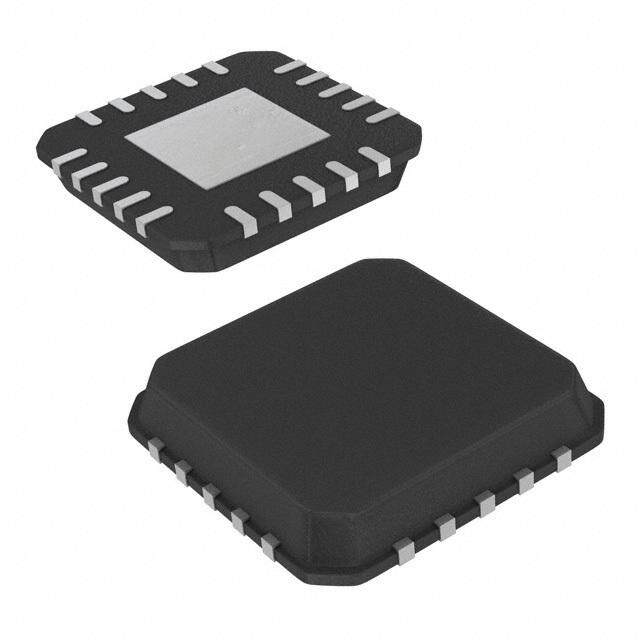
ICGOO电子元器件商城为您提供MCP4012T-503E/CH由Microchip设计生产,在icgoo商城现货销售,并且可以通过原厂、代理商等渠道进行代购。 MCP4012T-503E/CH价格参考¥3.51-¥4.64。MicrochipMCP4012T-503E/CH封装/规格:数据采集 - 数字电位器, Digital Potentiometer 50k Ohm 1 Circuit 64 Taps Up/Down (U/D, CS) Interface SOT-23-6。您可以下载MCP4012T-503E/CH参考资料、Datasheet数据手册功能说明书,资料中有MCP4012T-503E/CH 详细功能的应用电路图电压和使用方法及教程。
| 参数 | 数值 |
| 产品目录 | 集成电路 (IC)半导体 |
| 描述 | IC DGTL POT 50K 1CH RHEO SOT23-6数字电位计 IC 50k U/D single 6-bit V Rheostat |
| 产品分类 | |
| 品牌 | Microchip Technology |
| 产品手册 | |
| 产品图片 |
|
| rohs | 符合RoHS无铅 / 符合限制有害物质指令(RoHS)规范要求 |
| 产品系列 | 数字电位计 IC,Microchip Technology MCP4012T-503E/CH- |
| 数据手册 | http://www.microchip.com/mymicrochip/filehandler.aspx?ddocname=en025230http://www.microchip.com/mymicrochip/filehandler.aspx?ddocname=en023833 |
| 产品型号 | MCP4012T-503E/CH |
| POT数量 | Single |
| 产品目录页面 | |
| 产品种类 | 数字电位计 IC |
| 供应商器件封装 | SOT-23-6 |
| 其它名称 | MCP4012T-503E/CHDKR |
| 包装 | Digi-Reel® |
| 商标 | Microchip Technology |
| 存储器类型 | 易失 |
| 安装类型 | 表面贴装 |
| 安装风格 | SMD/SMT |
| 容差 | 20 % |
| 封装 | Reel |
| 封装/外壳 | SOT-23-6 |
| 封装/箱体 | SOT-23-6 |
| 工作温度 | -40°C ~ 125°C |
| 工作电源电压 | 5.5 V |
| 工厂包装数量 | 3000 |
| 弧刷存储器 | Volatile |
| 抽头 | 64 |
| 接口 | 2 线串行(芯片选择,增/减) |
| 描述/功能 | 64 step volatile digital POT |
| 数字接口 | 2-Wire |
| 最大工作温度 | + 125 C |
| 最小工作温度 | - 40 C |
| 标准包装 | 1 |
| 每POT分接头 | 64 |
| 温度系数 | 50 PPM / C |
| 电压-电源 | 1.8 V ~ 5.5 V |
| 电源电压-最大 | 5.5 V |
| 电源电压-最小 | 1.8 V |
| 电源电流 | 45 uA |
| 电路数 | 1 |
| 电阻 | 50 kOhms |
| 电阻(Ω) | 50k |


- 商务部:美国ITC正式对集成电路等产品启动337调查
- 曝三星4nm工艺存在良率问题 高通将骁龙8 Gen1或转产台积电
- 太阳诱电将投资9.5亿元在常州建新厂生产MLCC 预计2023年完工
- 英特尔发布欧洲新工厂建设计划 深化IDM 2.0 战略
- 台积电先进制程称霸业界 有大客户加持明年业绩稳了
- 达到5530亿美元!SIA预计今年全球半导体销售额将创下新高
- 英特尔拟将自动驾驶子公司Mobileye上市 估值或超500亿美元
- 三星加码芯片和SET,合并消费电子和移动部门,撤换高东真等 CEO
- 三星电子宣布重大人事变动 还合并消费电子和移动部门
- 海关总署:前11个月进口集成电路产品价值2.52万亿元 增长14.8%


PDF Datasheet 数据手册内容提取
MCP4011/2/3/4 Low-Cost 64-Step Volatile Digital POT Package Types Features • Volatile Digital Potentiometer in SOT-23, SOIC, MCP4011 MCP4012 MSOP and DFN packages SOIC, MSOP, DFN SOT-23-6 • 64 Taps: 63 Resistors with Taps to terminal A and Potentiometer Rheostat terminal B VDD 1 8 U/D VDD 1 A 6 A • Simple Up/Down (U/D) Protocol W VSS 2 7 NC VSS 2 5 W • Power-on Recall of Default Wiper Setting A B A 3 6 B U/D 3 B 4 CS - Custom POR wiper settings available (contact factory) W 4 W 5 CS • Resistance Values: 2.1kΩ, 5kΩ, 10kΩ or 50kΩ MCP4013 MCP4014 • Low Tempco: SOT-23-6 SOT-23-5 - Absolute (Rheostat): 50ppm (0°C to 70°C typ.) Potentiometer Rheostat - Ratiometric (Potentiometer): 10ppm (typ.) VDD 1 A 6 A VDD 1 W 5 W • Low Wiper Resistance: 75Ω (typ.) VSS 2 5 W VSS 2 B W B A • High-Voltage Tolerant Digital Inputs: Up to 12.5V U/D 3 4 CS U/D 3 4 CS • Low-Power Operation: 1µA Max Static Current • Wide Operating Voltage Range: Block Diagram - 1.8V to 5.5V - Device Operation A - 2.7V to 5.5V - Resistor Characteristics Specified VDD Power-Up and • Extended Temperature Range: -40°C to +125°C Brown-Out • Wide Bandwidth (-3 dB) Operation: VSS Control - 4MHz (typ.) for 2.1kΩ device gisterArray) DThees McrCiPp4ti0o11n/2/3/4 devices are volatile, 6-bit Digital UC/DS In2t-aeWnrfdaircee Wiper ReResistor W Potentiometers that can be configured as either a Control ( Logic potentiometer or rheostat. The wiper setting is controlled through a simple Up/Down (U/D) serial interface. B Device Features Resistance (typical) ™ y V ol ce ckog Device ConWfigipuerar tion MTeympoery POSRet Wtinipger Options (kΩ) W(iΩp)er S#te opfs ORpaenrgDaDeti n(2g) Contrnterfa perLochnol I WiTe MCP4011 Potentiometer (1) RAM Mid-Scale 2.1, 5.0, 10.0, 50.0 75 64 1.8V to 5.5V U/D No MCP4012 Rheostat RAM Mid-Scale 2.1, 5.0, 10.0, 50.0 75 64 1.8V to 5.5V U/D No MCP4013 Potentiometer RAM Mid-Scale 2.1, 5.0, 10.0, 50.0 75 64 1.8V to 5.5V U/D No MCP4014 Rheostat RAM Mid-Scale 2.1, 5.0, 10.0, 50.0 75 64 1.8V to 5.5V U/D No Note1: Floating either terminal (A or B) allows the device to be used in Rheostat mode. 2: Analog characteristics (resistor) tested from 2.7V to 5.5V. . © 2006 Microchip Technology Inc. DS21978C-page 1
MCP4011/2/3/4 1.0 ELECTRICAL † Notice: Stresses above those listed under “Maximum Ratings” may cause permanent damage to the device. This is CHARACTERISTICS a stress rating only and functional operation of the device at those or any other conditions above those indicated in the Absolute Maximum Ratings † operational listings of this specification is not implied. Exposure to maximum rating conditions for extended periods VDD............................................................................................................. 6.5V may affect device reliability. CS and U/D inputs w.r.t V -0.3V to 12.5V SS.................................... A,B and W terminals w.r.t V -0.3V to V + 0.3V SS..................... DD Current at Input Pins ..................................................±10mA Current at Supply Pins ...............................................±10mA Current at Potentiometer Pins ...................................±2.5mA Storage temperature.....................................-65°C to +150°C Ambient temp. with power applied................-55°C to +125°C ESD protection on all pins ...........≥ 4kV (HBM), ≥ 400V (MM) Maximum Junction Temperature (T )..........................+150°C J AC/DC CHARACTERISTICS Electrical Specifications: Unless otherwise indicated, all parameters apply across the specified operating ranges. T = -40°C to +125°C, 2.1kΩ, 5kΩ, 10kΩ and 50kΩ devices. Typical specifications represent values for V = 2.7V to 5.5V, A DD V = 0V, T = +25°C. SS A Parameters Sym Min Typ Max Units Conditions Operating Voltage Range V 2.7 — 5.5 V DD V — 1.8 — V V = 1.8V, CS:V = 8.5V, DD DD IHH V = 1.8V, V = 0V, IH IL U/D:V = 1.8V, V = 0V IH IL CS Input Voltage V V — 12.5 V The CS pin will be at one of three CS SS input levels (V , V or V ). IL IH IHH (Note6) Supply Current I — 45 — µA 5.5V, CS = V , f = 1MHz DD SS U/D — 15 — µA 2.7V, CS = V , f = 1MHz SS U/D — 0.3 1 µA Serial Interface Inactive (CS = V , U/D = V ) IH IH Resistance R 1.68 2.1 2.52 kΩ -202 devices (Note1) AB (± 20%) 4.0 5 6.0 kΩ -502 devices (Note1) 8.0 10 12.0 kΩ -103 devices (Note1) 40.0 50 60.0 kΩ -503 devices (Note1) Note 1: Resistance is defined as the resistance between terminal A to terminal B. 2: INL and DNL are measured at V with V = V and V = V .(-202 devices V = 4V). W A DD B SS A 3: MCP4011/13 only, test conditions are: I = 1.9mA, code = 00h. W 4: MCP4012/14 only, test conditions are: Current at Voltage Device Comments Resistance 5.5V 2.7V 2.1kΩ 2.25mA 1.1mA MCP4012 includes V WZSE 5kΩ 1.4mA 450µA MCP4014 includes VWFSE 10kΩ 450µA 210µA 50kΩ 90µA 40µA 5: Resistor terminals A, W and B’s polarity with respect to each other is not restricted. 6: This specification by design. 7: Non-linearity is affected by wiper resistance (R ), which changes significantly over voltage and temperature. See W Section6.0 “Resistor” for additional information. 8: For voltages below 2.7V, refer to Section2.0 “Typical Performance Curves”. 9: The MCP4011 is externally connected to match the configurations of the MCP4012 and MCP4014 and then tested. DS21978C-page 2 © 2006 Microchip Technology Inc.
MCP4011/2/3/4 AC/DC CHARACTERISTICS (CONTINUED) Electrical Specifications: Unless otherwise indicated, all parameters apply across the specified operating ranges. T = -40°C to +125°C, 2.1kΩ, 5kΩ, 10kΩ and 50kΩ devices. Typical specifications represent values for V = 2.7V to 5.5V, A DD V = 0V, T = +25°C. SS A Parameters Sym Min Typ Max Units Conditions Resolution N 64 Taps No Missing Codes Step Resistance RS — RAB / 63 — Ω Note6 Wiper Resistance (Note3, Note4) R — 70 125 Ω 5.5V W — 70 325 Ω 2.7V Nominal Resistance Tempco ΔR/ΔT — 50 — ppm/°C T = -20°C to +70°C A — 100 — ppm/°C T = -40°C to +85°C A — 150 — ppm/°C T = -40°C to +125°C A Ratiometeric Tempco ΔV /Δ — 10 — ppm/°C MCP4011 and MCP4013 only, WA T code = 1Fh Full-Scale Error (MCP4011/13 only) V -0.5 -0.1 +0.5 LSb Code 3Fh, 2.7V ≤ V ≤ 5.5V WFSE DD Zero-Scale Error (MCP4011/13 only) V -0.5 +0.1 +0.5 LSb Code 00h, 2.7V ≤ V ≤ 5.5V WZSE DD Monotonicity N Yes Bits Resistor Terminal Input Voltage Range V V Vss — V V Note5, Note6 A, W, DD (Terminals A, B and W) V B Current through A, W or B I — — 2.5 mA Note6 W Leakage current into A, W or B I — 100 — nA MCP4011 A = W = B = V WL SS — 100 — nA MCP4012/13 A = W = V SS — 100 — nA MCP4014 W = V SS Capacitance (P ) C — 75 — pF f =1MHz, code = 1Fh A AW Capacitance (P ) C — 120 — pF f =1MHz, code = 1Fh w W Capacitance (P ) C — 75 — pF f =1MHz, code = 1Fh B BW Bandwidth -3dB BW — 4 — MHz -202 Code = 1F, devices output load = 30pF — 2 — MHz -502 devices — 1 — MHz -103 devices — 200 — kHz -503 devices Note 1: Resistance is defined as the resistance between terminal A to terminal B. 2: INL and DNL are measured at V with V = V and V = V .(-202 devices V = 4V). W A DD B SS A 3: MCP4011/13 only, test conditions are: I = 1.9mA, code = 00h. W 4: MCP4012/14 only, test conditions are: Current at Voltage Device Comments Resistance 5.5V 2.7V 2.1kΩ 2.25mA 1.1mA MCP4012 includes V WZSE 5kΩ 1.4mA 450µA MCP4014 includes VWFSE 10kΩ 450µA 210µA 50kΩ 90µA 40µA 5: Resistor terminals A, W and B’s polarity with respect to each other is not restricted. 6: This specification by design. 7: Non-linearity is affected by wiper resistance (R ), which changes significantly over voltage and temperature. See W Section6.0 “Resistor” for additional information. 8: For voltages below 2.7V, refer to Section2.0 “Typical Performance Curves”. 9: The MCP4011 is externally connected to match the configurations of the MCP4012 and MCP4014 and then tested. © 2006 Microchip Technology Inc. DS21978C-page 3
MCP4011/2/3/4 AC/DC CHARACTERISTICS (CONTINUED) Electrical Specifications: Unless otherwise indicated, all parameters apply across the specified operating ranges. T = -40°C to +125°C, 2.1kΩ, 5kΩ, 10kΩ and 50kΩ devices. Typical specifications represent values for V = 2.7V to 5.5V, A DD V = 0V, T = +25°C. SS A Parameters Sym Min Typ Max Units Conditions Potentiometer Integral Non-linearity INL -0.5 ±0.25 +0.5 LSb MCP4011/13 only (Note2) Potentiometer Differential Non-linearity DNL -0.5 ±0.25 +0.5 LSb MCP4011/13 only (Note2) Rheostat Integral Non-linearity R-INL -0.5 ±0.25 +0.5 LSb -202 5.5V MCP4011 (Note4, Note9) devices -8.5 +4.5 +8.5 LSb 2.7V (Note7) MCP4012 and MCP4014 (Note4) (2.1kΩ) See Section2.0 LSb 1.8V (Note7, Note8) -0.5 ±0.25 +0.5 LSb -502 5.5V devices -5.5 +2.5 +5.5 LSb 2.7V (Note7) (5kΩ) See Section2.0 LSb 1.8V (Note7, Note8) -0.5 ±0.25 +0.5 LSb -103 5.5V devices -3 +1 +3 LSb 2.7V (Note7) (10kΩ) See Section2.0 LSb 1.8V (Note7, Note8) -0.5 ±0.25 +0.5 LSb -503 5.5V devices -1 +0.25 +1 LSb 2.7V (Note7) (50kΩ) See Section2.0 LSb 1.8V (Note7, Note8) Rheostat Differential Non-linearity R-DNL -0.5 ±0.25 +0.5 LSb -202 5.5V MCP4011 (Note4, Note9) devices -1 +0.5 +2 LSb 2.7V (Note7) MCP4012 and MCP4014 (Note4) (2.1kΩ) See Section2.0 LSb 1.8V (Note7, Note8) -0.5 ±0.25 +0.5 LSb -502 5.5V devices -1 +0.25 +1.25 LSb 2.7V (Note7) (5kΩ) See Section2.0 LSb 1.8V (Note7, Note8) -0.5 ±0.25 +0.5 LSb -103 5.5V devices -1 0 +1 LSb 2.7V (Note7) (10kΩ) See Section2.0 LSb 1.8V (Note7, Note8) -0.5 ±0.25 +0.5 LSb -503 5.5V devices -0.5 0 +0.5 LSb 2.7V (Note7) (50kΩ) See Section2.0 LSb 1.8V (Note7, Note8) Note 1: Resistance is defined as the resistance between terminal A to terminal B. 2: INL and DNL are measured at V with V = V and V = V .(-202 devices V = 4V). W A DD B SS A 3: MCP4011/13 only, test conditions are: I = 1.9mA, code = 00h. W 4: MCP4012/14 only, test conditions are: Current at Voltage Device Comments Resistance 5.5V 2.7V 2.1kΩ 2.25mA 1.1mA MCP4012 includes V WZSE 5kΩ 1.4mA 450µA MCP4014 includes VWFSE 10kΩ 450µA 210µA 50kΩ 90µA 40µA 5: Resistor terminals A, W and B’s polarity with respect to each other is not restricted. 6: This specification by design. 7: Non-linearity is affected by wiper resistance (R ), which changes significantly over voltage and temperature. See W Section6.0 “Resistor” for additional information. 8: For voltages below 2.7V, refer to Section2.0 “Typical Performance Curves”. 9: The MCP4011 is externally connected to match the configurations of the MCP4012 and MCP4014 and then tested. DS21978C-page 4 © 2006 Microchip Technology Inc.
MCP4011/2/3/4 AC/DC CHARACTERISTICS (CONTINUED) Electrical Specifications: Unless otherwise indicated, all parameters apply across the specified operating ranges. T = -40°C to +125°C, 2.1kΩ, 5kΩ, 10kΩ and 50kΩ devices. Typical specifications represent values for V = 2.7V to 5.5V, A DD V = 0V, T = +25°C. SS A Parameters Sym Min Typ Max Units Conditions Digital Inputs/Outputs (CS, U/D) Input High Voltage V 0.7V — — V IH DD Input Low Voltage V — — 0.3V V IL DD High-Voltage Input Entry Voltage V 8.5 — 12.5 (6) V Threshold for WiperLock™ IHH Technology High-Voltage Input Exit Voltage V — — V +0.8(6) V IHH DD CS Pull-up/Pull-down Resistance R — 16 — kΩ V = 5.5V, V = 3V CS DD CS CS Weak Pull-up/Pull-down Current I — 170 — µA V = 5.5V, V = 3V PU DD CS Input Leakage Current I -1 — 1 µA V = V IL IN DD CS and U/D Pin Capacitance C , — 10 — pF f = 1MHz, V ≥ 2.7V IN C DD C OUT RAM (Wiper) Value Value Range N 0h — 3Fh hex Default POR Setting N 1Fh hex Power Requirements Power Supply Sensitivity PSS — 0.0015 0.0035 %/% V = 4.5V to 5.5V, V = 4.5V, DD A (MCP4011 and MCP4013 only) Code = 1Fh — 0.0015 0.0035 %/% V = 2.7V to 4.5V, V = 2.7V, DD A Code = 1Fh Note 1: Resistance is defined as the resistance between terminal A to terminal B. 2: INL and DNL are measured at V with V = V and V = V .(-202 devices V = 4V). W A DD B SS A 3: MCP4011/13 only, test conditions are: I = 1.9mA, code = 00h. W 4: MCP4012/14 only, test conditions are: Current at Voltage Device Comments Resistance 5.5V 2.7V 2.1kΩ 2.25mA 1.1mA MCP4012 includes V WZSE 5kΩ 1.4mA 450µA MCP4014 includes VWFSE 10kΩ 450µA 210µA 50kΩ 90µA 40µA 5: Resistor terminals A, W and B’s polarity with respect to each other is not restricted. 6: This specification by design. 7: Non-linearity is affected by wiper resistance (R ), which changes significantly over voltage and temperature. See W Section6.0 “Resistor” for additional information. 8: For voltages below 2.7V, refer to Section2.0 “Typical Performance Curves”. 9: The MCP4011 is externally connected to match the configurations of the MCP4012 and MCP4014 and then tested. © 2006 Microchip Technology Inc. DS21978C-page 5
MCP4011/2/3/4 tCSLO tCSHI CS tLUC tLCUF tLO 1/fUD tLUC tLCUF U/D t HI t LCUR t S t S W FIGURE 1-1: Increment Timing Waveform. SERIAL TIMING CHARACTERISTICS Electrical Specifications: Unless otherwise noted, all parameters apply across the specified operating ranges. Extended (E): V = +1.8V to 5.5V, T = -40°C to +125°C. DD A Parameters Sym Min Typ Max Units Conditions CS Low Time t 5 — — µs CSLO CS High Time t 500 — — ns 2.7V ≤ V ≤ 5.5V CSHI DD — — — ns 1.8V ≤ V < 2.7V DD U/D to CS Hold Time t 500 — — ns 2.7V ≤ V ≤ 5.5V LUC DD 750 — — ns 1.8V ≤ V < 2.7V DD CS to U/D Low Setup Time t 500 — — ns LCUF CS to U/D High Setup Time t 3 — — µs LCUR U/D High Time t 500 — — ns HI U/D Low Time t 500 — — ns LO Up/Down Toggle Frequency f — — 1 MHz UD Wiper Settling Time t 0.5 — — µs 2.1kΩ, C = 100pF S L 1 — — µs 5kΩ, C = 100pF L 2 — — µs 10kΩ, C = 100pF L 10 5 — µs 50kΩ, C = 100pF L Wiper Response on Power-up t — 200 — ns PU DS21978C-page 6 © 2006 Microchip Technology Inc.
MCP4011/2/3/4 tCSLO tCSHI CS 1/f UD t tLUC tLCUF LUC t HI U/D tLCUR tLO t S t S W FIGURE 1-2: Decrement Timing Waveform. SERIAL TIMING CHARACTERISTICS Electrical Specifications: Unless otherwise noted, all parameters apply across the specified operating ranges. Extended (E): V = +1.8V to 5.5V, T = -40°C to +125°C. DD A Parameters Sym Min Typ Max Units Conditions CS Low Time t 5 — — µs CSLO CS High Time t 500 — — ns 2.7V ≤ V ≤ 5.5V CSHI DD — — — ns 1.8V ≤ V < 2.7V DD U/D to CS Hold Time t 500 — — ns 2.7V ≤ V ≤ 5.5V LUC DD 750 — — ns 1.8V ≤ V < 2.7V DD CS to U/D Low Setup Time t 500 — — ns LCUF CS to U/D High Setup Time t 3 — — µs LCUR U/D High Time t 500 — — ns HI U/D Low Time t 500 — — ns LO Up/Down Toggle Frequency f — — 1 MHz UD Wiper Settling Time t 0.5 — — µs 2.1kΩ, C = 100pF S L 1 — — µs 5kΩ, C = 100pF L 2 — — µs 10kΩ, C = 100pF L 10 5 — µs 50kΩ, C = 100pF L Wiper Response on Power-up t — 200 — ns PU © 2006 Microchip Technology Inc. DS21978C-page 7
MCP4011/2/3/4 tCSLO tCSHI 12V CS 5V tHUC tHCUF tLO 1/fUD tHUC tHCUF U/D t HI t HCUR t S t W S FIGURE 1-3: High-Voltage Increment Timing Waveform. SERIAL TIMING CHARACTERISTICS Electrical Specifications: Unless otherwise noted, all parameters apply across the specified operating ranges. Extended (E): V = +1.8V to 5.5V, T = -40°C to +125°C. DD A Parameters Sym Min Typ Max Units Conditions CS Low Time t 5 — — µs CSLO CS High Time t 500 — — ns 2.7V ≤ V ≤ 5.5V CSHI DD — — — ns 1.8V ≤ V < 2.7V DD U/D High Time t 500 — — ns HI U/D Low Time t 500 — — ns LO Up/Down Toggle Frequency f — — 1 MHz UD HV U/D to CS Hold Time t 1.5 — — µs HUC HV CS to U/D Low Setup Time t 8 — — µs HCUF HV CS to U/D High Setup Time t 4.5 — — µs HCUR Wiper Settling Time t 0.5 — — µs 2.1kΩ, C = 100pF S L 1 — — µs 5kΩ, C = 100pF L 2 — — µs 10kΩ, C = 100pF L 10 5 — µs 50kΩ, C = 100pF L Wiper Response on Power-up t — 200 — ns PU DS21978C-page 8 © 2006 Microchip Technology Inc.
MCP4011/2/3/4 tCSLO tCSHI 12V CS 5V 1/f UD t tHUC tHCUF HUC t HI U/D tHCUR tLO t S t S W FIGURE 1-4: High-Voltage Decrement Timing Waveform. SERIAL TIMING CHARACTERISTICS Electrical Specifications: Unless otherwise noted, all parameters apply across the specified operating ranges. Extended (E): V = +1.8V to 5.5V, T = -40°C to +125°C. DD A Parameters Sym Min Typ Max Units Conditions CS Low Time t 5 — — µs CSLO CS High Time t 500 — — ns 2.7V ≤ V ≤ 5.5V CSHI DD — — — ns 1.8V ≤ V < 2.7V DD U/D High Time t 500 — — ns HI U/D Low Time t 500 — — ns LO Up/Down Toggle Frequency f — — 1 MHz UD HV U/D to CS Hold Time t 1.5 — — µs HUC HV CS to U/D Low Setup Time t 8 — — µs HCUF HV CS to U/D High Setup Time t 4.5 — — µs HCUR Wiper Settling Time t 0.5 — — µs 2.1kΩ, C = 100pF S L 1 — — µs 5kΩ, C = 100pF L 2 — — µs 10kΩ, C = 100pF L 10 5 — µs 50kΩ, C = 100pF L Wiper Response on Power-up t — 200 — ns PU © 2006 Microchip Technology Inc. DS21978C-page 9
MCP4011/2/3/4 TEMPERATURE CHARACTERISTICS Electrical Specifications: Unless otherwise indicated, V =+2.7V to +5.5V, V =GND. DD SS Parameters Sym Min Typ Max Units Conditions Temperature Ranges Specified Temperature Range T -40 — +125 °C A Operating Temperature Range T -40 — +125 °C A Storage Temperature Range T -65 — +150 °C A Thermal Package Resistances Thermal Resistance, 5L-SOT-23 θ — 70 — °C/W JA Thermal Resistance, 6L-SOT-23 θ — 120 — °C/W JA Thermal Resistance, 8L-DFN (2x3) θ — 85 — °C/W JA Thermal Resistance, 8L-MSOP θ — 206 — °C/W JA Thermal Resistance, 8L-SOIC θ — 163 — °C/W JA DS21978C-page 10 © 2006 Microchip Technology Inc.
MCP4011/2/3/4 2.0 TYPICAL PERFORMANCE CURVES Note: The graphs and tables provided following this note are a statistical summary based on a limited number of samples and are provided for informational purposes only. The performance characteristics listed herein are not tested or guaranteed. In some graphs or tables, the data presented may be outside the specified operating range (e.g., outside specified power supply range) and therefore outside the warranted range. Note: Unless otherwise indicated, T = +25°C, V = 5V, V = 0V. A DD SS 80 250 1000 2.7V -40°C A) 70 2.7V 25°C 800 µ 2.7V 85°C 200 600 ce Current (I) (DD 2345600000 25555.....75555VVVVV 1-2814255205°°5°CC°°CCC R (kOhms)CS110500 ICS --0244200000000 I (µA)CS vi e 50 -600 D 10 RCS -800 0 0 -1000 0.20 0.40 0.60 0.80 1.00 9 8 7 6 5 4 3 2 1 f (MHz) V (V) U/D CS FIGURE 2-1: Device Current (I ) vs. U/D FIGURE 2-3: CS Pull-up/Pull-down DD Frequency (f ) and Ambient Temperature Resistance (R ) and Current (I ) vs. CS Input U/D CS CS (V = 2.7V and 5.5V). Voltage (V ) (V = 5.5V). DD CS DD 0.8 12 1.8V Entry 0.7 2.7V Entry Device Current (I) (µA)DD 000000......123456 VVDDDD == 25..75VV CS V Threshold (V)PP 124680 5125....5875VVVV EEEEnxxxiiittttry 0.0 0 -40 25 85 125 -40 -20 0 20 40 60 80 100 120 Ambient Temperature (°C) Ambient Temperature (°C) FIGURE 2-2: Device Current (I ) and FIGURE 2-4: CS High Input Entry/Exit SHDN V . (CS = V ) vs. Ambient Temperature. Threshold vs. Ambient Temperature and V . DD DD DD © 2006 Microchip Technology Inc. DS21978C-page 11
MCP4011/2/3/4 Note: Unless otherwise indicated, T = +25°C, V = 5V, V = 0V. A DD SS 140 0.075 120 0.8 -40C Rw 25C Rw 85C Rw 125C Rw -40C Rw 25C Rw 85C Rw 125C Rw 120 --4400CC IDNNLL 2255CC IDNNLL 8855CC IDNNLL 112255CC IDNNLL 0.05 100 --4400CC IDNNLL 2255CC IDNNLL 8855CC IDNNLL 112255CC IDNNLL 0.6 e e c 100 INL 0.025 c Wiper Resistan(Rw)(ohms) 468000 DNL --000..00525Error (LSb) Wiper Resistan(Rw)(ohms) 468000 INL 000..24Error (LSb) DNL 20 RW -0.075 20 RW -0.2 0 -0.1 0 -0.4 0 8 16 24 32 40 48 56 0 8 16 24 32 40 48 56 Wiper Setting (decimal) Wiper Setting (decimal) FIGURE 2-5: 2.1kΩ Pot Mode – R (Ω), FIGURE 2-8: 2.1kΩ Rheo Mode – R W W INL (LSb), DNL (LSb) vs. Wiper Setting and (Ω), INL (LSb), DNL (LSb) vs. Wiper Setting and Ambient Temperature (V = 5.5V). Ambient Temperature (V = 5.5V). DD DD 500 10 400 0.1 -40C Rw 25C Rw 85C Rw 125C Rw -40C Rw 25C Rw 85C Rw 125C Rw -40C INL 25C INL 85C INL 125C INL -40C INL 25C INL 85C INL 125C INL -40C DNL 25C DNL 85C DNL 125C DNL 8 Wiper Resistance (Rw)(ohms)123000000 -40C DINNDLLNL 25C DNL RW85C DNL 125C DNL -000.0.055Error (LSb) Wiper Resistance (Rw)(ohms)234000000 INL 246 Error (LSb) 100 0 0 -0.1 RW DNL 0 -2 0 8 16 24 32 40 48 56 0 8 16 24 32 40 48 56 Wiper Setting (decimal) Wiper Setting (decimal) FIGURE 2-6: 2.1kΩ Pot Mode – R (Ω), FIGURE 2-9: 2.1kΩ Rheo Mode – R W W INL (LSb), DNL (LSb) vs. Wiper Setting and (Ω), INL (LSb), DNL (LSb) vs. Wiper Setting and Ambient Temperature (V = 2.7V). Ambient Temperature (V = 2.7V). DD DD 1100 30 Wiper Resistance (Rw)(ohms)11345678901000000000000000000 ---444000CCC RIDNIwNNLDLLNL222555CCC RIDNwNLL RW888555CCC RIDNwNLL 111222555CCC RIDNwNLL ---00112100.....27272...27255555555Error (LSb) Wiper Resistance (Rw)(ohms)1345678900000000000000000 ---444000CCC RIDNwNLL 222555CCC RIDNwNLL INL888555CCC RIDNwNLL 111222555CCC RIDNwNLL 6811111222220246802468 Error (LSb) 200 -1.75 200 RW 4 100 -2.25 100 DNL 02 0 -2.75 0 -2 0 8 16 24 32 40 48 56 0 8 16 24 32 40 48 56 Wiper Setting (decimal) Wiper Setting (decimal) FIGURE 2-7: 2.1kΩ Pot Mode – R (Ω), FIGURE 2-10: 2.1kΩ Rheo Mode – R W W INL (LSb), DNL (LSb) vs. Wiper Setting and (Ω), INL (LSb), DNL (LSb) vs. Wiper Setting and Ambient Temperature (V = 1.8V). Ambient Temperature (V = 1.8V). DD DD DS21978C-page 12 © 2006 Microchip Technology Inc.
MCP4011/2/3/4 Note: Unless otherwise indicated, T = +25°C, V = 5V, V = 0V. A DD SS 2080 2500 ) B RA 2000 e ( 2060 al Resistanc(Ohms) 2040 VDD = 5.5V R (Ohms)WB11050000 -40°C n 2020 omi VDD = 2.7V 500 2855°°CC N 125°C 2000 0 -40 0 40 80 120 0 8 16 24 32 40 48 56 64 Ambient Temperature (°C) Wiper Setting (decimal) FIGURE 2-11: 2.1kΩ – Nominal FIGURE 2-12: 2.1kΩ – R (Ω) vs. Wiper WB Resistance (Ω) vs. Ambient Temperature and Setting and Ambient Temperature. V . DD © 2006 Microchip Technology Inc. DS21978C-page 13
MCP4011/2/3/4 Note: Unless otherwise indicated, T = +25°C, V = 5V, V = 0V. A DD SS WWIIPPEERR WIPER U/D U/D U/D FIGURE 2-13: 2.1kΩ – Low-Voltage FIGURE 2-16: 2.1kΩ – Low-Voltage Decrement Wiper Settling Time (V = 2.7V). Increment Wiper Settling Time (V = 2.7V). DD DD WIPER WIPER U/D U/D FIGURE 2-14: 2.1kΩ – Low-Voltage FIGURE 2-17: 2.1kΩ – Low-Voltage Decrement Wiper Settling Time (V = 5.5V). Increment Wiper Settling Time (V = 5.5V). DD DD WIPER V DD FIGURE 2-15: 2.1kΩ – Power-Up Wiper Response Time. DS21978C-page 14 © 2006 Microchip Technology Inc.
MCP4011/2/3/4 Note: Unless otherwise indicated, T = +25°C, V = 5V, V = 0V. A DD SS 140 0.075 120 0.6 -40C Rw 25C Rw 85C Rw 125C Rw -40C Rw 25C Rw 85C Rw 125C Rw 120 --4400CC IDNNLL 2255CC IDNNLL 8855CC IDNNLL 112255CC IDNNLL 0.05 100 --4400CC IDNNLL 2255CC IDNNLL 8855CC IDNNLL 112255CC IDNNLL 0.4 e e c 100 0.025 c Wiper Resistan(Rw)(ohms) 468000 INL DNL --000..00525Error (LSb) Wiper Resistan(Rw)(ohms) 468000 DNL RINWL -000.2.2Error (LSb) 20 RW -0.075 20 -0.4 0 -0.1 0 -0.6 0 8 16 24 32 40 48 56 0 8 16 24 32 40 48 56 Wiper Setting (decimal) Wiper Setting (decimal) FIGURE 2-18: 5kΩ Pot Mode – R (Ω), FIGURE 2-21: 5kΩ Rheo Mode – R (Ω), W W INL (LSb), DNL (LSb) vs. Wiper Setting and INL (LSb), DNL (LSb) vs. Wiper Setting and Ambient Temperature (V = 5.5V). Ambient Temperature (V = 5.5V). DD DD 450 0.1 600 5 -40C Rw 25C Rw 85C Rw 125C Rw -40C Rw 25C Rw 85C Rw 125C Rw 400 -40C INL 25C INL 85C INL 125C INL 0.075 -40C INL 25C INL 85C INL 125C INL -40C DNL 25C DNL 85C DNL 125C DNL 500 -40C DNL 25C DNL 85C DNL 125C DNL 4 e 350 0.05 e Wiper Resistanc(Rw)(ohms)112230505000000 DNL INL RW ---00000.0...0002752555Error (LSb) Wiper Resistanc(Rw)(ohms)234000000 INL 123 Error (LSb) 100 0 50 -0.1 RW DNL 0 -0.125 0 -1 0 8 16 24 32 40 48 56 0 8 16 24 32 40 48 56 Wiper Setting (decimal) Wiper Setting (decimal) FIGURE 2-19: 5kΩ Pot Mode – R (Ω), FIGURE 2-22: 5kΩ Rheo Mode – R (Ω), W W INL (LSb), DNL (LSb) vs. Wiper Setting and INL (LSb), DNL (LSb) vs. Wiper Setting and Ambient Temperature (V = 2.7V). Ambient Temperature (V = 2.7V). DD DD 2500 30 Wiper Resistance (Rw)(ohms)1122050500000000 ---444000CCC RIDNIwNLNDLLNL222555CCC RIDNwNLL R888W555CCC RIDNwNLL 111222555CCC RIDNwNLL ---00112100.....27272...27255555555Error (LSb) Wiper Resistance (Rw)(ohms)112050000000 ---444000CCC RIDNwNLL 222555CCC RIDNwNLL INL888555CCC RIDNwNLL 111222555CCC RIDNwNLL 6811111222220246802468 Error (LSb) 500 -1.75 500 RW 4 -2.25 DNL 2 0 0 -2.75 0 -2 0 8 16 24 32 40 48 56 0 8 16 24 32 40 48 56 Wiper Setting (decimal) Wiper Setting (decimal) FIGURE 2-20: 5kΩ Pot Mode – R (Ω), FIGURE 2-23: 5kΩ Rheo Mode – R (Ω), W W INL (LSb), DNL (LSb) vs. Wiper Setting and INL (LSb), DNL (LSb) vs. Wiper Setting and Ambient Temperature (V = 1.8V). Ambient Temperature (V = 1.8V). DD DD © 2006 Microchip Technology Inc. DS21978C-page 15
MCP4011/2/3/4 Note: Unless otherwise indicated, T = +25°C, V = 5V, V = 0V. A DD SS 4950 6000 ) AB 4925 5000 R e ( nc 4900 s) 4000 al Resista(Ohms) 44885705 VDD = 5.5V R (OhmWB 23000000 -40°C n omi 4825 1000 2855°°CC N VDD = 2.7V 125°C 4800 0 -40 -20 0 20 40 60 80 100 120 0 8 16 24 32 40 48 56 64 Ambient Temperature (°C) Wiper Setting (decimal) FIGURE 2-24: 5kΩ – Nominal Resistance FIGURE 2-25: 5kΩ – R (Ω) vs. Wiper WB (Ω) vs. Ambient Temperature and V . Setting and Ambient Temperature. DD DS21978C-page 16 © 2006 Microchip Technology Inc.
MCP4011/2/3/4 Note: Unless otherwise indicated, T = +25°C, V = 5V, V = 0V. A DD SS WIPER WIPER U/D U/D FIGURE 2-26: 5kΩ – Low-Voltage FIGURE 2-28: 5kΩ – Low-Voltage Decrement Wiper Settling Time (V = 2.7V). Increment Wiper Settling Time (V = 2.7V). DD DD WIPER WIPER U/D U/D FIGURE 2-27: 5kΩ – Low-Voltage FIGURE 2-29: 5kΩ – Low-Voltage Decrement Wiper Settling Time (V = 5.5V). Increment Wiper Settling Time (V = 5.5V). DD DD © 2006 Microchip Technology Inc. DS21978C-page 17
MCP4011/2/3/4 Note: Unless otherwise indicated, T = +25°C, V = 5V, V = 0V. A DD SS 120 0.05 120 0.15 -40C Rw 25C Rw 85C Rw 125C Rw -40C Rw 25C Rw 85C Rw 125C Rw -40C INL 25C INL 85C INL 125C INL -40C INL 25C INL 85C INL 125C INL 100 -40C DNL 25C DNL 85C DNL 125C DNL 0.025 100 -40C DNL 25C DNL 85C DNL 125C DNL 0.1 ce DNL ce INL per Resistan(Rw)(ohms) 468000 INL --000..00525Error (LSb) per Resistan(Rw)(ohms) 468000 DNL -000.0.055Error (LSb) Wi Wi RW RW 20 -0.075 20 -0.1 0 -0.1 0 -0.15 0 8 16 24 32 40 48 56 0 8 16 24 32 40 48 56 Wiper Setting (decimal) Wiper Setting (decimal) FIGURE 2-30: 10kΩ Pot Mode – R (Ω), FIGURE 2-33: 10kΩ Rheo Mode – R (Ω), W W INL (LSb), DNL (LSb) vs. Wiper Setting and INL (LSb), DNL (LSb) vs. Wiper Setting and Ambient Temperature (V = 5.5V). Ambient Temperature (V = 5.5V). DD DD 450 0.05 500 -40C Rw 25C Rw 85C Rw 125C Rw -40C Rw 25C Rw 85C Rw 125C Rw 400 -40C INL 25C INL 85C INL 125C INL -40C INL 25C INL 85C INL 125C INL 2.5 -40C DNL 25C DNL 85C DNL 125C DNL 0.025 -40C DNL 25C DNL 85C DNL 125C DNL ce 350 DNL 0 ce 400 INL 1.5 Wiper Resistan(Rw)(ohms)122350500000 INL RW ---000...00075255Error (LSb) Wiper Resistan(Rw)(ohms)230000 DNL RW -00.5.5 Error (LSb) 100 100 -1.5 -0.1 50 0 -0.125 0 -2.5 0 8 16 24 32 40 48 56 0 8 16 24 32 40 48 56 Wiper Setting (decimal) Wiper Setting (decimal) FIGURE 2-31: 10kΩ Pot Mode – R (Ω), FIGURE 2-34: 10kΩ Rheo Mode – R (Ω), W W INL (LSb), DNL (LSb) vs. Wiper Setting and INL (LSb), DNL (LSb) vs. Wiper Setting and Ambient Temperature (V = 2.7V). Ambient Temperature (V = 2.7V). DD DD 3500 30 Wiper Resistance (Rw)(ohms)112233050505000000000000 ---444000CCC RIDNwNLL 222555CCC RIDNwNLL 888555CCCD RIDINNNwNLLLL 111222555CCC RIDNwNLL ---00112100.....27272...27255555555Error (LSb) Wiper Resistance (Rw)(ohms)11223050500000000000 ---444000CCC RIDNwNLL R222555WCCC RIDNwNLL 888555CCC RIDNINwNLLL 111222555CCC RIDNwNLL 6811111222220246802468 Error (LSb) -1.75 4 500 RW -2.25 500 DNL 2 0 0 -2.75 0 -2 0 8 16 24 32 40 48 56 0 8 16 24 32 40 48 56 Wiper Setting (decimal) Wiper Setting (decimal) FIGURE 2-32: 10kΩ Pot Mode – R (Ω), FIGURE 2-35: 10kΩ Rheo Mode – R (Ω), W W INL (LSb), DNL (LSb) vs. Wiper Setting and INL (LSb), DNL (LSb) vs. Wiper Setting and Ambient Temperature (V = 1.8V). Ambient Temperature (V = 1.8V). DD DD DS21978C-page 18 © 2006 Microchip Technology Inc.
MCP4011/2/3/4 Note: Unless otherwise indicated, T = +25°C, V = 5V, V = 0V. A DD SS 10250 12000 R) AB 1100221300 10000 e ( 10190 nal Resistanc(Ohms)11110000111113570000 VDD = 5.5V R (Ohms)WB 468000000000 -40°C mi 10090 25°C o 2000 85°C N 10070 VDD = 2.7V 125°C 10050 0 -40 -20 0 20 40 60 80 100 120 0 8 16 24 32 40 48 56 64 Ambient Temperature (°C) Wiper Setting (decimal) FIGURE 2-36: 10kΩ – Nominal Resistance FIGURE 2-37: 10kΩ – R (Ω) vs. Wiper WB (Ω) vs. Ambient Temperature and V Setting and Ambient Temperature. DD. © 2006 Microchip Technology Inc. DS21978C-page 19
MCP4011/2/3/4 Note: Unless otherwise indicated, T = +25°C, V = 5V, V = 0V. A DD SS WIPER WIPER U/D U/D FIGURE 2-38: 10kΩ – Low-Voltage FIGURE 2-40: 10kΩ – Low-Voltage Decrement Wiper Settling Time (V = 2.7V). Increment Wiper Settling Time (V = 2.7V). DD DD WIPER WIPER U/D U/D FIGURE 2-39: 10kΩ – Low-Voltage FIGURE 2-41: 10kΩ – Low-Voltage Decrement Wiper Settling Time (V = 5.5V). Increment Wiper Settling Time (V = 5.5V). DD DD DS21978C-page 20 © 2006 Microchip Technology Inc.
MCP4011/2/3/4 Note: Unless otherwise indicated, T = +25°C, V = 5V, V = 0V. A DD SS 200 0.1 200 0.15 -40C Rw 25C Rw 85C Rw 125C Rw -40C Rw 25C Rw 85C Rw 125C Rw -40C INL 25C INL 85C INL 125C INL -40C INL 25C INL 85C INL 125C INL -40C DNL 25C DNL 85C DNL 125C DNL -40C DNL 25C DNL 85C DNL 125C DNL 160 0.05 0.1 e e 150 stancms)120 DNL 0 Sb) stancms) INL 0.05Sb) per Resi(Rw)(oh 80 INL RW -0.05Error (L per Resi(Rw)(oh100 RW 0 Error (L Wi Wi 50 40 -0.1 -0.05 DNL 0 -0.15 0 -0.1 0 8 16 24 32 40 48 56 0 8 16 24 32 40 48 56 Wiper Setting (decimal) Wiper Setting (decimal) FIGURE 2-42: 50kΩ Pot Mode – R (Ω), FIGURE 2-45: 50kΩ Rheo Mode – R (Ω), W W INL (LSb), DNL (LSb) vs. Wiper Setting and INL (LSb), DNL (LSb) vs. Wiper Setting and Ambient Temperature (V = 5.5V). Ambient Temperature (V = 5.5V). DD DD 600 0.05 600 1.5 -40C Rw 25C Rw 85C Rw 125C Rw -40C Rw 25C Rw 85C Rw 125C Rw -40C INL 25C INL 85C INL 125C INL -40C INL 25C INL 85C INL 125C INL 500 -40C DNL 25C DNL 85C DNL 125C DNL 0.025 500 -40C DNL 25C DNL 85C DNL 125C DNL 1 ce DNL ce RW stanms)400 0 Sb) stanms)400 INL 0.5 Sb) per Resi(Rw)(oh230000 INL --00..00525Error (L per Resi(Rw)(oh230000 DNL -00.5 Error (L Wi Wi 100 RW -0.075 100 -1 0 -0.1 0 -1.5 0 8 16 24 32 40 48 56 0 8 16 24 32 40 48 56 Wiper Setting (decimal) Wiper Setting (decimal) FIGURE 2-43: 50kΩ Pot Mode – R (Ω), FIGURE 2-46: 50kΩ Rheo Mode – R (Ω), W W INL (LSb), DNL (LSb) vs. Wiper Setting and INL (LSb), DNL (LSb) vs. Wiper Setting and Ambient Temperature (V = 2.7V). Ambient Temperature (V = 2.7V). DD DD 12000 30 12000 30 11000 --4400CC RINwL 2255CC RINwL 8855CC RINwL 112255CC RINwL 2268 11000 --4400CC RINwL 2255CC RINwL 8855CC RINwL 112255CC RINwL 2268 10000 -40C DNL 25C DNL 85C DNL 125C DNL 24 10000 -40C DNL 25C DNL 85C DNL 125C DNL 24 e 9000 22 e 9000 22 per Resistanc(Rw)(ohms) 45678000000000000000 RWINL 8111112024680 Error (LSb) per Resistanc(Rw)(ohms) 45678000000000000000 RWINL 8111112024680 Error (LSb) Wi 3000 6 Wi 3000 6 2000 DNL 4 2000 DNL 4 2 2 1000 0 1000 0 0 -2 0 -2 0 8 16 24 32 40 48 56 0 8 16 24 32 40 48 56 Wiper Setting (decimal) Wiper Setting (decimal) FIGURE 2-44: 50kΩ Pot Mode – R (Ω), FIGURE 2-47: 50kΩ Rheo Mode – R (Ω), W W INL (LSb), DNL (LSb) vs. Wiper Setting and INL (LSb), DNL (LSb) vs. Wiper Setting and Ambient Temperature (V = 1.8V). Ambient Temperature (V = 1.8V). DD DD © 2006 Microchip Technology Inc. DS21978C-page 21
MCP4011/2/3/4 Note: Unless otherwise indicated, T = +25°C, V = 5V, V = 0V. A DD SS 60000 49800 ) AB 49600 50000 R nce ( 4499240000 VDD = 5.5V s) 40000 nal Resista(Ohms)444889680000000 VDD = 2.7V R (OhmWB2300000000 -40C mi 48400 25C No 48200 10000 85C 125C 48000 0 -40 -20 0 20 40 60 80 100 120 0 8 16 24 32 40 48 56 64 Ambient Temperature (°C) Wiper Setting (decimal) FIGURE 2-48: 50kΩ – Nominal Resistance FIGURE 2-49: 50kΩ – R (Ω) vs. Wiper WB (Ω) vs. Ambient Temperature and V Setting and Ambient Temperature. DD. DS21978C-page 22 © 2006 Microchip Technology Inc.
MCP4011/2/3/4 Note: Unless otherwise indicated, T = +25°C, V = 5V, V = 0V. A DD SS U/D U/D WIPER WIPER FIGURE 2-50: 50kΩ – Low-Voltage FIGURE 2-53: 50kΩ – Low-Voltage Decrement Wiper Settling Time (V = 2.7V). Increment Wiper Settling Time (V = 2.7V). DD DD U/D U/D WIPER WIPER FIGURE 2-51: 50kΩ – Low-Voltage FIGURE 2-54: 50kΩ - Low-Voltage Decrement Wiper Settling Time (V = 5.5V). Increment Wiper Settling Time (V = 5.5V). DD DD WIPER V DD FIGURE 2-52: 50kΩ – Power-Up Wiper Response Time. © 2006 Microchip Technology Inc. DS21978C-page 23
MCP4011/2/3/4 Note: Unless otherwise indicated, T = +25°C, V = 5V, V = 0V. A DD SS 4.5 A z) 4 2.1 k(cid:58) +5V H 3.5 M W cy ( 3 VIN ~ + VOUT n 2.5 e equ 2 5 k(cid:58) Offset DUT - dB Fr 1.15 10 k(cid:58) Gnd B 3 - 0.5 50 k(cid:58) 0 2.5V DC -40 25 125 Temperature (°C) FIGURE 2-55: -3dB Bandwidth vs. FIGURE 2-56: -3dB Bandwidth Test Temperature. Circuit. DS21978C-page 24 © 2006 Microchip Technology Inc.
MCP4011/2/3/4 3.0 PIN DESCRIPTIONS The descriptions of the pins are listed in Table3-1. TABLE 3-1: PIN FUNCTION TABLE Pin Number Pin Buffer MCP4012 Symbol Function MCP4011 MCP4014 Type Type MCP4013 (SOIC-8) (SOT-23-5) (SOT-23-6) 1 1 1 V P — Positive Power Supply Input DD 2 2 2 V P — Ground SS 3 6 — A I/O A Potentiometer Terminal A 4 5 5 W I/O A Potentiometer Wiper Terminal 5 4 4 CS I TTL Chip Select Input 6 — — B I/O A Potentiometer Terminal B 7 — — NC — — No Connection 8 3 3 U/D I TTL Increment/Decrement Input Legend: TTL = TTL compatible input A = Analog input I = Input O = Output P = Power 3.1 Positive Power Supply Input (V ) 3.4 Potentiometer Wiper (W) Terminal DD The V pin is the device’s positive power supply input. The terminal W pin is connected to the internal potenti- DD The input power supply is relative to V and can range ometer’s terminal W (the wiper). The wiper terminal is SS from 1.8V to 5.5V. A decoupling capacitor on V (to the adjustable terminal of the digital potentiometer. The DD V ) is recommended to achieve maximum terminal W pin does not have a polarity relative to SS performance. terminals A or B pins. The terminal W pin can support both positive and negative current. The voltage on 3.2 Ground (VSS) terminal W must be between VSS and VDD. The VSS pin is the device ground reference. 3.5 Potentiometer Terminal B 3.3 Potentiometer Terminal A The terminal B pin is connected to the internal potenti- ometer’s terminal B (available on some devices). The The terminal A pin is connected to the internal potenti- potentiometer’s terminal B is the fixed connection to the ometer’s terminal A (available on some devices). The 0x00 terminal of the digital potentiometer. potentiometer’s terminal A is the fixed connection to the The terminal B pin is available on the MCP4011 device. 0x3F terminal of the digital potentiometer. The terminal B pin does not have a polarity relative to The terminal A pin is available on the MCP4011, the terminal W or A pins. The terminal B pin can MCP4012 and MCP4013 devices. The terminal A pin support both positive and negative current. The voltage does not have a polarity relative to the terminal W or B on terminal B must be between V and V . SS DD pins. The terminal A pin can support both positive and The terminal B pin is not available on the MCP4012, negative current. The voltage on terminal A must be MCP4013 and MCP4014 devices. between V and V . SS DD For the MCP4013 and MCP4014, the internal potenti- The terminal A pin is not available on the MCP4014. ometer’s terminal B is internally connected to V . The potentiometer’s terminal A is internally floating. SS Terminal B does not have a polarity relative to terminals W or A. Terminal B can support both positive and negative current. For the MCP4012, terminal B is internally floating. © 2006 Microchip Technology Inc. DS21978C-page 25
MCP4011/2/3/4 3.6 Chip Select (CS) 3.7 Increment/Decrement (U/D) The CS pin is the chip select input. Forcing the CS pin The U/D pin input is used to increment or decrement to V enables the serial commands. These commands the wiper on the digital potentiometer. An increment IL can increment and decrement the wiper. Forcing the moves the wiper one step toward terminal A, while a CS pin to V enables the high-voltage serial decrement moves the wiper one step toward IHH commands. These commands can increment and terminalB. decrement the wiper and are compatibe with the MCP402X devices. The wiper is saved to volatile memory (RAM). The CS pin has an internal pull-up resistor. The resistor will become “disabled” when the voltage on the CS pin is below the V level. This means that when the CS pin IH is “floating”, the CS pin will be pulled to the V level IH (serial communication (the U/D pin) is ignored). And when the CS pin is driven low (V ), the resistance IL becomes very large to reduce the device current consumption when serial commands are occurring. See Figure2-3 for additional information. DS21978C-page 26 © 2006 Microchip Technology Inc.
MCP4011/2/3/4 4.0 GENERAL OVERVIEW EQUATION 4-1: R CALCULATION S The MCP4011/2/3/4 devices are general purpose R = R----A----B- digital potentiometers intended to be used in S 63 applications where a programmable resistance with moderate bandwidth is desired. EQUATION 4-2: R CALCULATION WB Applications generally suited for the MCP4011/2/3/4 R N devices include: R = ----A----B------+R WB 63 W • Set point or offset trimming • Sensor calibration N = 0 to 63 (decimal) • Selectable gain and offset amplifier designs 1LSb is the ideal resistance difference between two • Cost-sensitive mechanical trim pot replacement successive codes. If we use N = 1 and R = 0 in W The digital potentiometer is available in four nominal Equation4-2, we can calculate the step size for each resistances (R ), where the nominal resistance is increment or decrement command. AB defined as the resistance between terminal A and The MCP4011 device offers a voltage divider terminal B. The four nominal resistances are 2.1kΩ, (potentiometer) with all terminals available on pins. 5kΩ, 10kΩ and 50kΩ. The MCP4012 is a true rheostat, with terminal A and There are 63 resistors in a string between terminal A the wiper (W) of the variable resistor available on pins. and terminal B. The wiper can be set to tap onto any of The MCP4013 device offers a voltage divider (potenti- these 63 resistors thus providing 64 possible settings ometer) with terminal B connected to ground. (including terminal A and terminal B). The MCP4014 device is a Rheostat device with Figure4-1 shows a block diagram for the resistive terminal A of the resistor floating, terminal B connected network of the device. Equation4-1 shows the to ground, and the wiper (W) available on pin. calculation for the step resistance, while Equation4-2 illustrates the calculation used to determine the The MCP4011 can be externally configured to resistance between the wiper and terminal B. implement any of the MCP4012, MCP4013 or MCP4014 configurations. A 4.1 Serial Interface N = 63 3Fh R (1) A 2-wire synchronous serial protocol is used to R W increment or decrement the digital potentiometer’s S wiper terminal. The Increment/Decrement (U/D) N = 62 3Eh protocol utilizes the CS and U/D input pins. Both inputs RS RW (1) are tolerant of signals up to 12.5V without damaging the device. The CS pin can differenciate between two N = 61 3Dh high-voltage levels, V and V . This enables IH IHH R RW (1) additional commands without requiring additional input S pins. The high-voltage commands (V on the CS pin) IHH are similar to the standard commands and are supported for compatability to the MCP401X family of W devices. N = 1 01h The simple U/D protocol uses the state of the U/D pin R (1) at the falling edge of the CS pin to determine if RS W Increment or Decrement mode is desired. Subsequent rising edges of the U/D pin move the wiper. N = 0 00h R (1) The wiper value will not underflow or overflow. W B Analog Mux Note1: The wiper resistance is tap dependent. That is, each tap selection resistance has a small variation. This variation effects the smaller resistance devices (2.1kΩ) more. FIGURE 4-1: Resistor Block Diagram. © 2006 Microchip Technology Inc. DS21978C-page 27
MCP4011/2/3/4 4.2 Power-up 4.3 Brown Out When the device powers up (rising V crosses the If the device V is below the specified minimum DD DD Trip Point Voltage (V )), the “default” wiper setting is voltage, care must be taken to ensure that the CS and TP restored. Table4-1 shows the default value loaded into U/D pins do not “create” any of the serial commands. the wiper on POR/BOR. When the device V drops below V (1.8V), the DD MIN electrical performance may not meet the data sheet TABLE 4-1: DEFAULT POR WIPER specifications (see Figure4-2). The wiper state may be SETTING SELECTION unknown. Also, the device may be capable of incrementing or decrementing, if a valid command is Default detected on the CS and U/D pins. Package POR Wiper Typical Code Wiper Code R Value When the device voltage rises from below the power- AB Setting up trip point (V ) into the valid operation voltage TP range, the wiper state will be forced to the default POR -202 Mid-scale 1Fh 2.1kΩ wiper setting (see Table4-1). -502 Mid-scale 1Fh 5.0kΩ -103 Mid-scale 1Fh 10.0kΩ 4.4 Serial Interface Inactive -503 Mid-scale 1Fh 50.0kΩ The serial interface is inactive any time the CS pin is at V and all write cycles are completed. IH While V < V (1.8V), the electrical performance DD min may not meet the data sheet specifications (see Figure4-2). The wiper state may be unknown. Also, the device may be capable of incrementing or decrement- ing, if a valid command is detected on the CS and U/D pins. V DD 1.8V V TP V SS POR Trip Point (on Rising V ) DD Outside Device Operation Wiper Forced to Default POR Setting FIGURE 4-2: Power-up and Brown-out. DS21978C-page 28 © 2006 Microchip Technology Inc.
MCP4011/2/3/4 5.0 SERIAL INTERFACE 5.2 Serial Commands The MCP401X devices support eight serial commands. 5.1 Overview Six of these commands are for support and to ease migration with the MCP402X family of devices. The The MCP4011/2/3/4 utilizes a simple 2-wire interface to commands can be grouped into the following types: increment or decrement the digital potentiometer’s wiper terminal (W). This interface uses the CS and U/D • Serial Commands pins. The CS pin is the Chip Select input, while the U/D • High-voltage Serial Commands pin is the Up/Down input. All the commands are shown in Table5-1. The Increment/Decrement protocol enables the device The command type is determined by the voltage level to move one step at a time through the range of the CS pin is driven to. The initial state that the CS pin possible resistance values. The wiper value is must be driven is V . From V , the two levels that the initialized with the “default” value upon power-up. IH IH CS pin can be driven are: A wiper value of 00h connects the wiper to terminal B. • V A wiper value of 3Fh connects the wiper to terminal A. IL • V Increment commands move the wiper toward terminal IHH A, but will not increment to a value greater than 3Fh. If the CS pin is driven from V to V , a serial IH IL Decrement commands move the wiper toward terminal command is selected. If the CS pin is driven from V to IH B, but will not decrement below 00h. V , a high-voltage serial command is selected. IHH Refer to Section1.0 “Electrical Characteristics”, Support of the high-voltage serial commands is for AC/DC Electrical Characteristics table for detailed input compatiblity with the MCP402X devices. threshold and timing specifications. Communication is unidirectional. Therefore, the value of the current wiper setting cannot be read out of the MCP401X device. TABLE 5-1: COMMANDS High Voltage Command Name on CS pin? Increment — Increment (for MCP402X Compatibility) — Decrement — Decrement (for MCP402X Compatibility) — High-Voltage Increment 1 (for MCP402X Compatibility) Yes High-Voltage Increment 2 (for MCP402X Compatibility) Yes High-Voltage Decrement 1 (for MCP402X Compatibility) Yes High-Voltage Decrement 2 (for MCP402X Compatibility) Yes © 2006 Microchip Technology Inc. DS21978C-page 29
MCP4011/2/3/4 5.2.1 INCREMENT When the device voltage falls below the RAM retention voltage of the device, the wiper state may be corrupted. This mode is achieved by initializing the U/D pin to a When the device returns to the operating range, the high state (V ) prior to achieving a low state (V ) on the IH IL wiper will be loaded with the default POR wiper setting. CS pin. Subsequent rising edges of the U/D pin increment the wiper setting toward terminal A. This is After the CS pin is driven to VIH (from VIL), any other shown in Figure5-1. serial command may immediately be entered. After the wiper is incremented to the desired position, Note: The wiper value will not overflow. That is, the CS pin should be forced to VIH to ensure that once the wiper value equals 0x3F, “unexpected” transitions on the U/D pin do not cause subsequent increment commands are the wiper setting to increment. Driving the CS pin to VIH ignored. should occur as soon as possible (within device specifications) after the last desired increment occurs. V IH CS VIL 1 2 3 4 5 6 VIH U/D V IL X X+1 X+2 X+3 X+4 Wiper FIGURE 5-1: Increment. DS21978C-page 30 © 2006 Microchip Technology Inc.
MCP4011/2/3/4 5.2.2 INCREMENT (FOR MCP402X When the device voltage falls below the RAM retention COMPATIBILITY) voltage of the device, the wiper state may be corrupted. When the device returns to the operating range, the Note: This command allows compatibility with wiper will be loaded with the Default POR wiper setting. the MCP402X family, which supports After the CS pin is driven to V (from V ), any other updating of the non-volatile wiper setting. IH IL serial command may immediately be entered. This mode is achieved by initializing the U/D pin to a high state (V ) prior to achieving a low state (V ) on the Note: The wiper value will not overflow. That is, IH IL CS pin. Subsequent rising edges of the U/D pin once the wiper value equals 0x3F, increments the wiper setting toward terminal A. This is subsequent increment commands are shown in Figure5-2. ignored. After the wiper is incremented to the desired position, the U/D pin should be driven low (V ), and the CS pin IL should be forced to V to ensure that “unexpected” IH transitions on the U/D pin do not cause the wiper setting to increment. Driving the CS pin to V should IH occur as soon as possible (within device specifications) after the last desired increment occurs. V V IH IH CS VIL V 1 2 3 4 5 6 IH U/D VIL X X+1 X+2 X+3 X+4 Wiper FIGURE 5-2: Increment (For MCP402X Compatibility). © 2006 Microchip Technology Inc. DS21978C-page 31
MCP4011/2/3/4 5.2.3 DECREMENT When the device voltage falls below the RAM retention voltage of the device, the wiper state may be corrupted. This mode is achieved by initializing the U/D pin to a low When the device returns to the operating range, the state (V ) prior to achieving a low state (V ) on the CS IL IL wiper will be loaded with the default POR wiper setting. pin. Subsequent rising edges of the U/D pin will decrement the wiper setting toward terminal B. This is After the CS pin is driven to VIH (from VIL), any other shown in Figure5-3. serial command may immediately be entered. After the wiper is decremented to the desired position, Note: The wiper value will not underflow. That is, the U/D pin should be forced low (VIL) and the CS pin once the wiper value equals 0x00, should be forced to VIH. This will ensure that subsequent decrement commands are “unexpected” transitions on the U/D pin do not cause ignored. the wiper setting to decrement. Driving the CS pin to V should occur as soon as possible (within device IH specifications) after the last desired increment occurs. V IH CS VIL 1 2 3 4 V 5 6 IH U/D VIL VIL X X-1 X-2 X-3 X-4 Wiper FIGURE 5-3: Decrement. DS21978C-page 32 © 2006 Microchip Technology Inc.
MCP4011/2/3/4 5.2.4 DECREMENT (FOR MCP402X When the device voltage falls below the RAM retention COMPATIBILITY) voltage of the device, the wiper state may be corrupted. When the device returns to the operating range, the Note: This command allows compatibility with wiper will be loaded with the default POR wiper setting. the MCP402X family, which supports After the CS pin is driven to V (from V ), any other updating of the non-volatile wiper setting. IH IL serial command may immediately be entered. This mode is achieved by initializing the U/D pin to a low state (V ) prior to achieving a low state (V ) on the Note: The wiper value will not underflow. That is, IL IL CS pin. Subsequent rising edges of the U/D pin once the wiper value equals 0x00, decrement the wiper setting toward terminal B. This is subsequent decrement commands are shown in Figure5-4. ignored. After the wiper is decremented to the desired position, the U/D pin should remain high (V ), and the CS pin IH should be forced to V to ensure that “unexpected” IH transitions on the U/D pin do not cause the wiper setting to increment. Driving the CS pin to V should IH occur as soon as possible (within device specifications) after the last desired increment occurs. V IH CS VIL 1 2 3 4 5 6 VIH U/D VIL X X-1 X-2 X-3 X-4 Wiper FIGURE 5-4: Decrement (For MCP402X Compatibility). © 2006 Microchip Technology Inc. DS21978C-page 33
MCP4011/2/3/4 5.2.5 HIGH-VOLTAGE INCREMENT 1 After the CS pin is driven to V (from V ), any other IH IL (FOR MCP402X COMPATIBILITY) serial command may immediately be entered. Note: This command allows compatibility with Note: The wiper value will not overflow. That is, the MCP402X family, which supports once the wiper value equals 0x3F, updating of the non-volatile wiper setting subsequent increment commands are with the WiperLock Technology feature. ignored. This mode is achieved by initializing the U/D pin to a high state (V ) prior to the CS pin being driven to V . IH IHH Subsequent rising edges of the U/D pin increment the wiper setting toward terminal A. Set the U/D pin to the high state (V ) prior to forcing the CS pin to V . This IH IH is shown in Figure5-5. V IHH V V IH IH CS VIH 1 2 3 4 5 6 VIH U/D V IL X X+1 X+2 X+3 X+4 Wiper FIGURE 5-5: High-Voltage Increment 1 (For MCP402X Compatibility). DS21978C-page 34 © 2006 Microchip Technology Inc.
MCP4011/2/3/4 5.2.6 HIGH-VOLTAGE INCREMENT 2 After the CS pin is driven to V (from V ), any other IH IL (FOR MCP402X COMPATIBILITY) serial command may immediately be entered. Note: This command allows compatibility with Note: The wiper value will not overflow. That is, the MCP402X family, which supports once the wiper value equals 0x3F, updating of the non-volatile wiper setting subsequent increment commands are with the WiperLock Technology feature. ignored. This mode is achieved by initializing the U/D pin to a high state (V ) prior to the CS pin being driven to V . IH IHH Subsequent rising edges of the U/D pin increment the wiper setting toward terminal A. Set the U/D pin to the low state (V ) prior to forcing the CS pin to V . This is IL IH shown in Figure5-6. V IHH V V IH IH CS VIH 1 2 3 4 5 6 U/D V VIL IL X X+1 X+2 X+3 X+4 Wiper FIGURE 5-6: High-Voltage Increment 2 (For MCP402X Compatibility). © 2006 Microchip Technology Inc. DS21978C-page 35
MCP4011/2/3/4 5.2.7 HIGH-VOLTAGE DECREMENT 1 After the CS pin is driven to V (from V ), any other IH IL (FOR MCP402X COMPATIBILITY) serial command may immediately be entered. Note: This command allows compatibility with Note: The wiper value will not underflow. That is, the MCP402X family, which supports once the wiper value equals 0x00, updating of the non-volatile wiper setting subsequent decrement commands are with the WiperLock Technology feature. ignored. This mode is achieved by initializing the U/D pin to a low state (V ) prior to the CS pin being driven to V . IL IHH Subsequent rising edges of the U/D pin decrement the wiper setting toward terminal B. Set the U/D pin to the low state (V ) prior to forcing the CS pin to V . This is IL IH shown in Figure5-7. V IHH V V IH IH CS 1 2 3 4 5 6 V IH U/D V V IL IL X X-1 X-2 X-3 X-4 Wiper FIGURE 5-7: High-Voltage Decrement 1 (For MCP402X Compatibility). DS21978C-page 36 © 2006 Microchip Technology Inc.
MCP4011/2/3/4 5.2.8 HIGH-VOLTAGE DECREMENT 2 After the CS pin is driven to V (from V ), any other IH IL (FOR MCP402X COMPATIBILITY) serial command may immediately be entered. Note: This command allows compatibility with Note: The wiper value will not underflow. That is, the MCP402X family, which supports once the wiper value equals 0x00, updating of the non-volatile wiper setting subsequent decrement commands are with the WiperLock Technology feature. ignored. This mode is achieved by initializing the U/D pin to the low state (V ) prior to driving the CS pin to V . IL IHH Subsequent rising edges of the U/D pin decrement the wiper setting toward terminal B. Set the U/D pin to a high state (V ) prior to forcing the CS pin to V . This IH IH is shown in Figure5-8. V IHH V V IH IH CS 1 2 3 4 VDD 5 6 VIH U/D V IL X X-1 X-2 X-3 X-4 Wiper FIGURE 5-8: High-Voltage Decrement 2 (For MCP402X Compatibility). © 2006 Microchip Technology Inc. DS21978C-page 37
MCP4011/2/3/4 5.3 CS High Voltage Step resistance (R ) is the resistance from one tap S setting to the next. This value will be dependent on the The CS pin is High-Voltage (VIHH) tolerant, like the RAB value that has been selected. Table6-1 shows the MCP402X. This allows the MCP401X to be used in typical step resistances for each device. MCP402X applications without needing to change The total resistance of the device has minimal variation other portions of the application circuit. due to operating voltage (see Figure2-11, Figure2-24, Figure2-36 or Figure2-48). 6.0 RESISTOR TABLE 6-1: TYPICAL STEP RESISTANCES Digital potentiometer applications can be divided into two categories: Typical Resistance (Ω) Part Number • Rheostat configuration Total (R ) Step (R ) AB S • Potentiometer (or voltage divider) configuration MCP401X-203E 2100 33.33 Figure6-1 shows a block diagram for the MCP401X MCP401X-503E 5000 79.37 resistors. MCP401X-104E 10000 158.73 A MCP401X-504E 50000 793.65 N = 63 3Fh R (1) Terminal A and B, as well as the wiper W, do not have RS W a polarity. These terminals can support both positive and negative current. N = 62 3Eh RS RW (1) N = 61 3Dh R (1) R W S W N = 1 01h R (1) R W S N = 0 00h R (1) W B Analog Mux Note1: The wiper resistance is tap dependent. That is, each tap selection resistance has a small variation. This variation effects the smaller resistance devices (2.1kΩ) more. FIGURE 6-1: Resistor Block Diagram. DS21978C-page 38 © 2006 Microchip Technology Inc.
MCP4011/2/3/4 6.1 Resistor Configurations 6.1.2 POTENTIOMETER CONFIGURATION 6.1.1 RHEOSTAT CONFIGURATION When used as a potentiometer, all three terminals are When used as a rheostat, two of the three digital poten- tied to different nodes in the circuit. This allows the tiometer’s terminals are used as a resistive element in potentiometer to output a voltage proportional to the the circuit. With terminal W (wiper) and either terminal input voltage. This configuration is sometimes called A or terminal B, a variable resistor is created. The voltage divider mode. The potentiometer is used to resistance will depend on the tap setting of the wiper provide a variable voltage by adjusting the wiper and the wiper’s resistance. The resistance is controlled position between the two endpoints as shown in by changing the wiper setting. Figure6-3. Reversing the polarity of the A and B The unused terminal (B or A) should be left floating. terminals will not affect operation. Figure6-2 shows the two possible resistors that can be used. Reversing the polarity of the A and B terminals V 1 will not affect operation. A V A W 3 B W RAW or RBW V 2 B FIGURE 6-3: Potentiometer Configuration. Resistor The temperature coefficient of the RAB resistors is minimal by design. In this configuration, the resistors all FIGURE 6-2: Rheostat Configuration. change uniformly, so minimal variation should be seen. This allows the control of the total resistance between The wiper resistor temperature coefficient is different the two nodes. The total resistance depends on the from the RAB temperature coefficient. The voltage at “starting” terminal to the wiper terminal. At the code node V3 (Figure6-3) is not dependent on this wiper 00h, the RBW resistance is minimal (RW), but the RAW resistance, just the ratio of the RAB resistors, so this resistance in maximized (R + R ). Conversely, at the temperature coefficient in most cases can be AB W code 3Fh, the R resistance is minimal (R ), but the ignored. AW W R resistance in maximized (R + R ). BW AB W Note: To avoid damage to the internal wiper The resistance step size (R ) equates to one LSb of the circuitry in this configuration, care should S resistor. be taken to insure the current flow never exceeds 2.5mA. Note: To avoid damage to the internal wiper circuitry in this configuration, care should be taken to insure the current flow never exceeds 2.5mA. The change in wiper-to-end terminal resistance over temperature is shown in Figure2-11, Figure2-24, Figure2-36 and Figure2-48. The most variation over temperature will occur in the first few codes due to the wiper resistance coefficient affecting the total resistance. The remaining codes are dominated by the total resistance tempco R . AB © 2006 Microchip Technology Inc. DS21978C-page 39
MCP4011/2/3/4 6.2 Wiper Resistance The slope of the resistance has a linear area (at the higher voltages) and a non-linear area (at the lower Wiper resistance is the series resistance of the wiper. voltages), where resistance increases faster than the This resistance is typically measured when the wiper is voltage drop (at low voltages). positioned at either zero-scale (00h) or full-scale (3Fh). The wiper resistance in potentiometer-generated voltage divider applications is not a significant source of error. The wiper resistance in rheostat applications can create significant non-linearity as the wiper is moved RW toward zero-scale (00h). The lower the nominal resistance, the greater the possible error. Wiper resistance is significant depending on the devices operating voltage. As the device voltage V DD decreases, the wiper resistance increases (see Figure6-4 and Table6-2). Note: The slope of the resistance has a linear In a rheostat configuration, this change in voltage area (at the higher voltages) and a non- needs to be taken into account, particularly for the linear area (at the lower voltages). lower resistance devices. For the 2.1kΩ device, the FIGURE 6-4: Relationship of Wiper maximum wiper resistance at 5.5V is approximately 6% of the total resistance, while at 2.7V, it is approximately Resistance (RW) to Voltage. 15.5% of the total resistance. Since there is minimal variation of the total device In a potentiometer configuration, the wiper resistance resistance over voltage, at a constant temperature (see variation does not effect the output voltage seen on the Figure2-11, Figure2-24, Figure2-36 or Figure2-48), terminal W pin. the change in wiper resistance over voltage can have a significant impact on the INL and DNL error. TABLE 6-2: TYPICAL STEP RESISTANCES AND RELATIONSHIP TO WIPER RESISTANCE Resistance (Ω) R / R (%) (1, 2) R / R (%) (1, 3) W S W AB Typical Wiper (R ) W R = R = Max R = Max R = R = Max R = Max W W W W W W Total Step Max @ Max @ Typical @ 5.5V @ 2.7V Typical @ 5.5V @ 2.7V Typical (R ) (R ) 5.5V 2.7V AB S 2100 33.33 75 125 325 225.0% 375.0% 975.0% 3.57% 5.95% 15.48% 5000 79.37 75 125 325 94.5% 157.5% 409.5% 1.5% 2.50% 6.50% 10000 158.73 75 125 325 47.25% 78.75% 204.75% 0.75% 1.25% 3.25% 50000 793.65 75 125 325 9.45% 15.75% 40.95% 0.15% 0.25% 0.65% Note1: The wiper resistance (R ) is not a significant source of error in potentiometer-generated voltage divider W applications. In rheostat applications, the variation of the R value can create significant non-linearity. W 2: R is the typical value. The variation of this resistance is minimal over voltage. S 3: R is the typical value. The variation of this resistance is minimal over voltage. AB DS21978C-page 40 © 2006 Microchip Technology Inc.
MCP4011/2/3/4 6.3 Operational Characteristics 6.3.1.2 Differential Non-Linearity (DNL) Understanding the operational characteristics of the DNL error is the measure of variations in code widths device’s resistor components is important to the system from the ideal code width. A DNL error of zero would design. imply that every code is exactly 1LSb wide. 6.3.1 ACCURACY 6.3.1.1 Integral Non-Linearity (INL) 111 INL error for these devices is the maximum deviation 110 between an actual code transition point and its Actual Transfer corresponding ideal transition point after offset and 101 Function gain errors have been removed. These endpoints are from 0x00 to 0x3F. Refer to Figure6-5. Digital 100 Ideal Transfer Input Function Positive INL means higher resistance than ideal. Code 011 Negative INL means lower resistance than ideal. 010 Wide Code, > 1 LSb 001 INL < 0 000 111 Narrow Code < 1 LSb Actual 110 Rransfer Digital Pot Output Function 101 FIGURE 6-6: DNL Accuracy. Digital 100 6.3.1.3 Ratiometric Temperature Coefficient Input Code 011 The ratiometric temperature coefficient quantifies the Ideal Transfer error in the ratio R /R due to temperature drift. Function AW WB 010 This is typically the critical error when using a potentiometer device (MCP4011 and MCP4013) in a 001 voltage divider configuration. 000 6.3.1.4 Absolute Temperature Coefficient INL < 0 The absolute temperature coefficient quantifies the error in the end-to-end resistance (nominal resistance Digital Pot Output R ) due to temperature drift. This is typically the AB critical error when using a rheostat device (MCP4012 FIGURE 6-5: INL Accuracy. and MCP4014) in an adjustable resistor configuration. © 2006 Microchip Technology Inc. DS21978C-page 41
MCP4011/2/3/4 6.3.2 MONOTONIC OPERATION Monotonic operation means that the device’s resistance increases with every step change (from terminal A to terminal B or terminal B to terminal A). The wiper resistance is different at each tap location. When changing from one tap position to the next (either increasing or decreasing), the ΔR is less than the W ΔR . When this change occurs, the device voltage and S temperature are “the same” for the two tap positions. R S63 0x3F R S62 0x3E e d 0x3D o C ut p n R al I 0x03 S3 git R Di 0x02 S1 R S0 0x01 0x00 R W n = ? (@ tap) R = R + R BW Sn W(@ Tap n) n = 0 Resistance (R ) BW FIGURE 6-7: Resistance R . BW DS21978C-page 42 © 2006 Microchip Technology Inc.
MCP4011/2/3/4 7.0 DESIGN CONSIDERATIONS 7.2 Layout Considerations In the design of a system with the MCP401X devices, Inductively-coupled AC transients and digital switching the following considerations should be taken into noise can degrade the input and output signal integrity, account: potentially masking the MCP4011/2/3/4’s performance. Careful board layout will minimize these effects and • The Power Supply increase the Signal-to-Noise Ratio (SNR). Bench • The Layout testing has shown that a multi-layer board utilizing a low-inductance ground plane, isolated inputs, isolated 7.1 Power Supply Considerations outputs and proper decoupling are critical to achieving the performance that the silicon is capable of providing. The typical application will require a bypass capacitor Particularly harsh environments may require shielding in order to filter high-frequency noise, which can be of critical signals. induced onto the power supply's traces. The bypass capacitor helps to minimize the effect of these noise If low noise is desired, breadboards and wire-wrapped sources on signal integrity. Figure7-1 illustrates an boards are not recommended. appropriate bypass strategy. In this example, the recommended bypass capacitor value is 0.1µF. This capacitor should be placed as close (within 4mm) to the device power pin (V ) as DD possible. The power source supplying these devices should be as clean as possible. If the application circuit has separate digital and analog power supplies, V and DD V should reside on the analog plane. SS V DD 0.1µF V DD 0.1µF r e oll r nt o c A 3/4 cro 2/ U/D Mi W 1/ ® 1 C 40 PI P B MC CS V V SS SS FIGURE 7-1: Typical Microcontroller Connections. © 2006 Microchip Technology Inc. DS21978C-page 43
MCP4011/2/3/4 8.0 APPLICATIONS EXAMPLES V Non-volatile digital potentiometers have a multitude of DD practical uses in modern electronic circuits. The most popular uses include precision calibration of set point R 1 thresholds, sensor trimming, LCD bias trimming, audio MCP4011 attenuation, adjustable power supplies, motor control A overcurrent trip setting, adjustable gain amplifiers and CS W V offset trimming. The MCP4011/2/3/4 devices can be OUT U/D used to replace the common mechanical trim pot in B applications where the operating and terminal voltages are within CMOS process limitations (V = 2.7V to DD R 2 5.5V). 8.1 Set Point Threshold Trimming FIGURE 8-1: Using the Digital Applications that need accurate detection of an input threshold event often need several sources of error Potentiometer to Set a Precise Output Voltage. eliminated. Use of comparators and operational 8.1.1 TRIMMING A THRESHOLD FOR AN amplifiers (op amps) with low offset and gain error can help achieve the desired accuracy, but in many OPTICAL SENSOR applications, the input source variation is beyond the If the application has to calibrate the threshold of a designer’s control. If the entire system can be diode, transistor or resistor, a variation range of 0.1V is calibrated after assembly in a controlled environment common. Often, the desired resolution of 2mV or (like factory test), these sources of error are minimized, better is adequate to accurately detect the presence of if not entirely eliminated. a precise signal. A “windowed” voltage divider, utilizing Figure8-1 illustrates a common digital potentiometer the MCP4011 or MCP4013, would be a potential configuration. This configuration is often referred to as solution as shown in Figure8-2. a “windowed voltage divider”. Note that R and R are 1 2 not necessary to create the voltage divider, but their V presence is useful when the desired threshold has DD limited range. It is “windowed” because R and R can 1 2 narrow the adjustable range of V to a value much TRIP less than V – V . If the output range is reduced, the DD SS magnitude of each output step is reduced. This effectively increases the trimming resolution for a fixed VDD V CC+ digital potentiometer resolution. This technique may R sense allow a lower-cost digital potentiometer to be utilized R 1 (64 steps instead of 256 steps). MCP4011 A Comparator The MCP4011’s and MCP4013’s low DNL performance V is critical to meeting calibration accuracy in production CS W TRIP MCP6021 without having to use a higher precision digital U/D potentiometer. B 0.1µF VCC– R 2 EQUATION 8-1: CALCULATING THE WIPER SETTING FROM THE DESIRED V TRIP FIGURE 8-2: Set Point or Threshold V = V ⎛------R----2----+-----R----W----B--------⎞ Calibration. TRIP DD⎝R +R +R ⎠ 1 AB 2 R = R AB Nominal R = R •⎛-D-----⎞ WB AB ⎝63⎠ V D = ⎛⎛----T---R----I-P--⎞ •((R +R +R )–R )⎞ •63 ⎝⎝ V ⎠ 1 AB 2 2 ⎠ DD Where: D = Digital Potentiometer Wiper Setting (0-63) DS21978C-page 44 © 2006 Microchip Technology Inc.
MCP4011/2/3/4 8.2 Operational Amplifier V Applications DD VIN + MCP6291 Figure8-3, Figure8-4 and Figure8-5 illustrate typical V Op Amp amplifier circuits that could replace fixed resistors with DD V the MCP4011/2/3/4 to achieve digitally-adjustable W – VOUT analog solutions. R1 Figure8-4 shows a circuit that allows a non-inverting amplifier to have its’ offset and gain to be independently 11 A R3 40 W A W trimmed. The MCP4011 is used along with resistors R1 CP B and R2 to set the offset voltage. The sum of R1 + R2 M resistance should be significantly greater (> 100 times) MCP4012 R the resistance value of the MCP4011. This allows each 2 increment or decrement in the MCP4011 to be a fine adjustment of the offset voltage. The input voltage of the op amp (V ) should be centered at the op amps V FIGURE 8-4: Trimming Offset and Gain in IN w voltage. The gain is adjusted by the MCP4012. If the a Non-Inverting Amplifier. resistance value of the MCP4012 is small compared to the resistance value of R , then this is a fine adjustment 3 MCP4011 of the gain. If the resistance value of the MCP4012 is R R 3 4 equal (or large) compared to the resistance value of R , A B 3 then this is a course adjustment of the gain. In general, W trim the course adjustments first and then trim the fine Pot 2 adjustments. VDD – Op Amp MCP4011 R1 V R3 R4 VIN + MCP6021 OUT A B V A IN W W 1 B Pot1 fc = 2----π----⋅----R-----------⋅---C--- V – Eq DD MCP4011 R Op Amp 2 R 1 V + OUT 011 A W MCP6001 TEhqeuviveanleinnt REq = (R1+RAB–RWB)||(R2+RWB)+Rw 4 P C B M FIGURE 8-5: Programmable Filter. R 2 FIGURE 8-3: Trimming Offset and Gain in an Inverting Amplifier. © 2006 Microchip Technology Inc. DS21978C-page 45
MCP4011/2/3/4 8.3 Temperature Sensor Applications V DD Thermistors are resistors with very predictable variation with temperature. Thermistors are a popular sensor choice when a low-cost, temperature-sensing R 1 solution is desired. Unfortunately, thermistors have NTC non-linear characteristics that are undesirable, typically Thermistor requiring trimming in an application to achieve greater accuracy. There are several common solutions to trim and linearize thermistors. Figure8-6 and Figure8-7 are simple methods for linearizing a 3-terminal NTC MCP4011 thermistor. Both are simple voltage dividers using a V OUT Positive Temperature Coefficient (PTC) resistor (R ) 1 with a transfer function capable of compensating for the linearity error in the Negative Temperature Coefficient R 2 (NTC) thermistor. The circuit, illustrated by Figure8-6, utilizes a digital rheostat for trimming the offset error caused by the FIGURE 8-7: Thermistor Calibration using thermistor’s part-to-part variation. This solution puts the a Digital Potentiometer in a Potentiometer digital potentiometer’s R into the voltage divider W Configuration. calculation. The MCP4011/2/3/4’s R temperature AB coefficient is 50ppm (-20°C to +70°C). R ’s error is W 8.4 Wheatstone Bridge Trimming substantially greater than R ’s error because R AB W varies with V , wiper setting and temperature. For the DD Another common configuration to “excite” a sensor 50kΩ devices, the error introduced by R is, in most W (such as a strain gauge, pressure sensor or thermistor) cases, insignificant as long as the wiper setting is > 6. is the wheatstone bridge configuration. The wheat- For the 2kΩ devices, the error introduced by R is W stone bridge provides a differential output instead of a significant because it is a higher percentage of R . WB single-ended output. Figure8-8 illustrates a For these reasons, the circuit illustrated in Figure8-6 is wheatstone bridge utilizing one to three digital not the most optimum method for “exciting” and potentiometers. The digital potentiometers in this linearizing a thermistor. example are used to trim the offset and gain of the wheatstone bridge. V DD V DD R 1 NTC Thermistor VOUT MCP4012 2.1kΩ R 2 A MCP4012 V W OUT FIGURE 8-6: Thermistor Calibration using MCP4012 MCP4012 a Digital Potentiometer in a Rheostat 50kΩ 50kΩ Configuration. The circuit illustrated by Figure8-7 utilizes a digital FIGURE 8-8: Wheatstone Bridge potentiometer for trimming the offset error. This solution removes R from the trimming equation along Trimming. W with the error associated with R . R is not required, W 2 but can be utilized to reduce the trimming “window” and reduce variation due to the digital potentiometer’s R AB part-to-part variability. DS21978C-page 46 © 2006 Microchip Technology Inc.
MCP4011/2/3/4 9.0 DEVELOPMENT SUPPORT 9.1 Evaluation/Demonstration Boards Currently there are three boards that are available that can be used to evaluate the MCP401X family of devices. 1. The MCP402X Digital Potentiometer Evaluation Board kit (MCP402XEV) contains a simple dem- onstration board utilizing a PIC10F206, the MCP401X and a blank PCB, which can be pop- ulated with any desired MCP4011/2/3/4 device in a SOT-23-5, SOT-23-6 or 150mil SOIC 8-pin package. This board has two push buttons to control when the PIC® microcontroller generates MCP402X serial commands. The example firmware demonstrates the following commands: • Increment • Decrement • High-Voltage Increment and Enable WiperLock Technology • High-Voltage Decrement and Enable WiperLock Technology • High-Voltage Increment and Disable WiperLock Technology • High-Voltage Decrement and Disable WiperLock Technology The populated board (with the MCP4011) can be used to evaluate the other MCP401X devices by appropriately jumpering the PCB pads. 2. The SOT-23-5/6 Evaluation Board (VSUPEV2) can be used to evaluate the characteristics of the MCP4012, MCP4013 and MCP4014 devices. 3. The 8-pin SOIC/MSOP/TSSOP/DIP Evaluation Board (SOIC8EV) can be used to evaluate the characteristics of the MCP4011 device in either the SOIC or MSOP package. 4. The MCP4XXX Digital Potentiometer Daughter Board allows the system designer to quickly evaluate the operation of Microchip Technol- ogy's MCP42XXX and MCP402X Digital Poten- tiometers. The board supports two MCP42XXX devices and an MCP402X device, which can be replaced with an MCP401X device. The board also has a voltage doubler device (TC1240A), which can be used to show the WiperLock™ Technology feature of the MCP4021. These boards may be purchased directly from the Microchip web site at www.microchip.com. © 2006 Microchip Technology Inc. DS21978C-page 47
MCP4011/2/3/4 10.0 PACKAGING INFORMATION 10.1 Package Marking Information 5-Lead SOT-23 (MCP4014) Example: XXNN JU25 Part Number Code MCP4014T-202E/OT JUNN MCP4014T-502E/OT JVNN MCP4014T-103E/OT JWNN MCP4014T-503E/OT JXNN Note: Applies to 5-Lead SOT-23 6-Lead SOT-23 (MCP4012 / MCP4013) Example: XXNN BJ25 Code Part Number MCP4012 MCP4013 MCP401xT-202E/CH BJNN BPNN MCP401xT-502E/CH BKNN BQNN MCP401xT-103E/CH BLNN BRNN MCP401xT-503E/CH BMNN BSNN Note: Applies to 6-Lead SOT-23 Legend: XX...X Customer-specific information Y Year code (last digit of calendar year) YY Year code (last 2 digits of calendar year) WW Week code (week of January 1 is week ‘01’) NNN Alphanumeric traceability code e3 Pb-free JEDEC designator for Matte Tin (Sn) * This package is Pb-free. The Pb-free JEDEC designator ( e 3 ) can be found on the outer packaging for this package. Note: In the event the full Microchip part number cannot be marked on one line, it will be carried over to the next line, thus limiting the number of available characters for customer-specific information. DS21978C-page 48 © 2006 Microchip Technology Inc.
MCP4011/2/3/4 Package Marking Information 8-Lead DFN (2x3) (MCP4011) Example: XXX ABE YWW 534 NNN 256 Part Number Code MCP4011T-202E/MC ABE MCP4011T-502E/MC ABF MCP4011T-103E/MC ABG MCP4011T-503E/MC ABH Note: Applies to 8-Lead DFN 8-Lead MSOP (MCP4011) Example: XXXXXX 401122 YWWNNN 534256 8-Lead SOIC (150 mil) (MCP4011) Example: XXXXXXXX 401152E XXXXYYWW SN^e^3 0534 NNN 256 Part Numbers Code 8L-MSOP 8L-SOIC MCP4011-202E/MS MCP4011-202E/SN 22 MCP4011-502E/MS MCP4011-502E/SN 52 MCP4011-103E/MS MCP4011-103E/SN 13 MCP4011-503E/MS MCP4011-503E/SN 53 Legend: XX...X Customer-specific information Y Year code (last digit of calendar year) YY Year code (last 2 digits of calendar year) WW Week code (week of January 1 is week ‘01’) NNN Alphanumeric traceability code e3 Pb-free JEDEC designator for Matte Tin (Sn) * This package is Pb-free. The Pb-free JEDEC designator ( e 3 ) can be found on the outer packaging for this package. Note: In the event the full Microchip part number cannot be marked on one line, it will be carried over to the next line, thus limiting the number of available characters for customer-specific information. © 2006 Microchip Technology Inc. DS21978C-page 49
MCP4011/2/3/4 5-Lead Plastic Small Outline Transistor (OT) (SOT-23) Note: For the most current package drawings, please see the Microchip Packaging Specification located at http://www.microchip.com/packaging E E1 p B p1 D n 1 α c A A2 φ A1 L β Units INCHES* MILLIMETERS Dimension Limits MIN NOM MAX MIN NOM MAX Number of Pins n 5 5 Pitch p .038 0.95 Outside lead pitch (basic) p1 .075 1.90 Overall Height A .035 .046 .057 0.90 1.18 1.45 Molded Package Thickness A2 .035 .043 .051 0.90 1.10 1.30 Standoff A1 .000 .003 .006 0.00 0.08 0.15 Overall Width E .102 .110 .118 2.60 2.80 3.00 Molded Package Width E1 .059 .064 .069 1.50 1.63 1.75 Overall Length D .110 .116 .122 2.80 2.95 3.10 Foot Length L .014 .018 .022 0.35 0.45 0.55 Foot Angle f 0 5 10 0 5 10 Lead Thickness c .004 .006 .008 0.09 0.15 0.20 Lead Width B .014 .017 .020 0.35 0.43 0.50 Mold Draft Angle Top a 0 5 10 0 5 10 Mold Draft Angle Bottom b 0 5 10 0 5 10 *Controlling Parameter Notes: Dimensions D and E1 do not include mold flash or protrusions. Mold flash or protrusions shall not exceed .005" (0.127mm) per side. EIAJ Equivalent: SC-74A Drawing No. C04-091 Revised 09-12-05 DS21978C-page 50 © 2006 Microchip Technology Inc.
MCP4011/2/3/4 6-Lead Plastic Small Outline Transistor (CH) (SOT-23) Note: For the most current package drawings, please see the Microchip Packaging Specification located at http://www.microchip.com/packaging E E1 B p1 D n 1 α c φ A A2 β L A1 Units INCHES* MILLIMETERS Dimension Limits MIN NOM MAX MIN NOM MAX Number of Pins n 6 6 Pitch p .038 BSC 0.95 BSC Outside lead pitch p1 .075 BSC 1.90 BSC Overall Height A .035 .046 .057 0.90 1.18 1.45 Molded Package Thickness A2 .035 .043 .051 0.90 1.10 1.30 Standoff A1 .000 .003 .006 0.00 0.08 0.15 Overall Width E .102 .110 .118 2.60 2.80 3.00 Molded Package Width E1 .059 .064 .069 1.50 1.63 1.75 Overall Length D .110 .116 .122 2.80 2.95 3.10 Foot Length L .014 .018 .022 0.35 0.45 0.55 Foot Angle φ 0 5 10 0 5 10 Lead Thickness c .004 .006 .008 0.09 0.15 0.20 Lead Width B .014 .017 .020 0.35 0.43 0.50 Mold Draft Angle Top α 0 5 10 0 5 10 Mold Draft Angle Bottom β 0 5 10 0 5 10 *Controlling Parameter Notes: Dimensions D and E1 do not include mold flash or protrusions. Mold flash or protrusions shall not exceed .005" (0.127mm) per side. BSC: Basic Dimension. Theoretically exact value shown without tolerances. See ASME Y14.5M JEITA (formerly EIAJ) equivalent: SC-74A Revised 09-12-05 Drawing No. C04-120 © 2006 Microchip Technology Inc. DS21978C-page 51
MCP4011/2/3/4 8-Lead Plastic Dual-Flat No-Lead Package (MC) 2x3x0.9 mm Body (DFN) – Saw Singulated Note: For the most current package drawings, please see the Microchip Packaging Specification located at http://www.microchip.com/packaging D e b N N L K E E2 EXPOSED PAD NOTE 1 NOTE 1 1 2 2 1 D2 TOP VIEW BOTTOM VIEW A NOTE 2 A3 A1 Units MILLIMETERS Dimension Limits MIN NOM MAX Number of Pins N 8 Pitch e 0.50 BSC Overall Height A 0.80 0.90 1.00 Standoff A1 0.00 0.02 0.05 Contact Thickness A3 0.20 REF Overall Length D 2.00 BSC Overall Width E 3.00 BSC Exposed Pad Length D2 1.30 — 1.75 Exposed Pad Width E2 1.50 — 1.90 Contact Width b 0.18 0.25 0.30 Contact Length § L 0.30 0.40 0.50 Contact-to-Exposed Pad § K 0.20 — — Notes: 1. Pin 1 visual index feature may vary, but must be located within the hatched area. 2. Package may have one or more exposed tie bars at ends. 3. § Significant Characteristic 4. Package is saw singulated 5. Dimensioning and tolerancing per ASME Y14.5M BSC: Basic Dimension. Theoretically exact value shown without tolerances. REF: Reference Dimension, usually without tolerance, for information purposes only. Microchip Technology Drawing No. C04–123, Sept. 8, 2006 DS21978C-page 52 © 2006 Microchip Technology Inc.
MCP4011/2/3/4 8-Lead Plastic Micro Small Outline Package (MS) (MSOP) Note: For the most current package drawings, please see the Microchip Packaging Specification located at http://www.microchip.com/packaging D N E E1 NOTE 1 1 2 e b c ϕ A A2 A1 L1 L Units MILLIMETERS Dimension Limits MIN NOM MAX Number of Pins N 8 Pitch e 0.65 BSC Overall Height A — — 1.10 Molded Package Thickness A2 0.75 0.85 0.95 Standoff A1 0.00 — 0.15 Overall Width E 4.90 BSC Molded Package Width E1 3.00 BSC Overall Length D 3.00 BSC Foot Length L 0.40 0.60 0.80 Footprint L1 0.95 REF Foot Angle ϕ 0° — 8° Lead Thickness c 0.08 — 0.23 Lead Width b 0.22 — 0.40 Notes: 1. Pin 1 visual index feature may vary, but must be located within the hatched area. 2. Dimensions D and E1 do not include mold flash or protrusions. Mold flash or protrusions shall not exceed 0.15 mm per side. 3. Dimensioning and tolerancing per ASME Y14.5M BSC: Basic Dimension. Theoretically exact value shown without tolerances. REF: Reference Dimension, usually without tolerance, for information purposes only. Microchip Technology Drawing No. C04–111, Sept. 8, 2006 © 2006 Microchip Technology Inc. DS21978C-page 53
MCP4011/2/3/4 8-Lead Plastic Small Outline (SN) – Narrow, 150 mil (SOIC) Note: For the most current package drawings, please see the Microchip Packaging Specification located at http://www.microchip.com/packaging E E1 p D 2 B n 1 h α 45° c A A2 φ β L A1 Units INCHES* MILLIMETERS Dimension Limits MIN NOM MAX MIN NOM MAX Number of Pins n 8 8 Pitch p .050 1.27 Overall Height A .053 .061 .069 1.35 1.55 1.75 Molded Package Thickness A2 .052 .056 .061 1.32 1.42 1.55 Standoff § A1 .004 .007 .010 0.10 0.18 0.25 Overall Width E .228 .237 .244 5.79 6.02 6.20 Molded Package Width E1 .146 .154 .157 3.71 3.91 3.99 Overall Length D .189 .193 .197 4.80 4.90 5.00 Chamfer Distance h .010 .015 .020 0.25 0.38 0.51 Foot Length L .019 .025 .030 0.48 0.62 0.76 Foot Angle φ 0 4 8 0 4 8 Lead Thickness c .008 .009 .010 0.20 0.23 0.25 Lead Width B .013 .017 .020 0.33 0.42 0.51 Mold Draft Angle Top α 0 12 15 0 12 15 Mold Draft Angle Bottom β 0 12 15 0 12 15 * Controlling Parameter § Significant Characteristic Notes: Dimensions D and E1 do not include mold flash or protrusions. Mold flash or protrusions shall not exceed .010” (0.254mm) per side. JEDEC Equivalent: MS-012 Drawing No. C04-057 DS21978C-page 54 © 2006 Microchip Technology Inc.
MCP4011/2/3/4 APPENDIX A: REVISION HISTORY Revision C (December 2006) • Added device designators in conditions column to associate units (MHz) in Bandwidth -3dB parameter in AC/DC Characteristics table. • Added device designations in conditions column for R-INL and R-DNL specifications. Revision B (October 2006) • For the 10kΩ device, the rheostat differential non-linearity specification at 2.7V was changed from ±0.5 LSb to ±1 LSb. • Figure 2-9 in Section2.0 “Typical Performance Curves” was updated with the correct data. • Added Figure 2-55 for -3db Bandwidth information. • Added Figure 2-56 for -3db Bandwidth test circuit. • Updated available Development Tools • Added disclaimer to package outline drawings and updated changed drawings as needed. Revision A (November 2005) • Original Release of this Document. © 2006 Microchip Technology Inc. DS21978C-page 55
MCP4011/2/3/4 NOTES: DS21978C-page 56 © 2006 Microchip Technology Inc.
MCP4011/2/3/4 PRODUCT IDENTIFICATION SYSTEM To order or obtain information, e.g., on pricing or delivery, refer to the factory or the listed sales office. PART NO. XXX X /XX Examples: a) MCP4011-103E/MS: 10kΩ, 8-LD MSOP Device Resistance Temperature Package b) MCP4011-103E/SN: 10kΩ, 8-LD SOIC Version Range c) MCP4011T-103E/MC: T/R, 10kΩ, 8-LD DFN d) MCP4011T-103E/MS: T/R, 10kΩ, 8-LD MSOP e) MCP4011T-103E/SN: T/R, 10kΩ, 8-LD SOIC f) MCP4011-202E/MS: 2.1kΩ, 8-LD MSOP Device: MCP4011: Single Potentiometer with U/D Interface g) MCP4011-202E/SN: 2.1kΩ, 8-LD SOIC MCP4011T: Single Potentiometer with U/D Interface h) MCP4011T-202E/MC: T/R, 2.1kΩ, 8-LD DFN (Tape and Reel) (SOIC, MSOP) i) MCP4011T-202E/MS: T/R, 2.1kΩ, 8-LD MSOP MCP4012: Single Rheostat with U/D interface j) MCP4011T-202E/SN: T/R, 2.1kΩ, 8-LD SOIC MCP4012T: Single Rheostat with U/D interface k) MCP4011-502E/MS: 5kΩ, 8-LD MSOP (Tape and Reel) (SOT-23-6) l) MCP4011-502E/SN: 5kΩ, 8-LD SOIC MCP4013: Single Potentiometer to GND with U/D m) MCP4011T-502E/MC: T/R, 5kΩ, 8-LD DFN Interface n) MCP4011T-502E/MS: T/R, 5kΩ, 8-LD MSOP MCP4013T: Single Potentiometer to GND with U/D o) MCP4011T-502E/SN: T/R, 5kΩ, 8-LD SOIC Interface (Tape and Reel) (SOT-23-6) p) MCP4011-503E/MS: 50kΩ, 8-LD MSOP MCP4014: Single Rheostat to GND with U/D q) MCP4011-503E/SN: 50kΩ, 8-LD SOIC Interface r) MCP4011T-503E/MC: T/R, 50kΩ, 8-LD DFN MCP4014T: Single Rheostat to GND with U/D s) MCP4011T-503E/MS: T/R, 50kΩ, 8-LD MSOP Interface (Tape and Reel)(SOT-23-5) t) MCP4011T-503E/SN: T/R, 50kΩ, 8-LD SOIC a) MCP4012T-202E/CH 2.1kΩ, 6-LD SOT-23 Resistance Version: 202 = 2.1kΩ b) MCP4012T-502E/CH 5kΩ, 6-LD SOT-23 502 = 5kΩ c) MCP4012T-103E/CH 10kΩ, 6-LD SOT-23 103 = 10kΩ d) MCP4012T-503E/CH 50kΩ, 6-LD SOT-23 503 = 50kΩ a) MCP4013T-202E/CH 2.1kΩ, 6-LD SOT-23 b) MCP4013T-502E/CH 5kΩ, 6-LD SOT-23 Temperature Range: E = -40°C to +125°C c) MCP4013T-103E/CH 10kΩ, 6-LD SOT-23 d) MCP4013T-503E/CH 50kΩ, 6-LD SOT-23 Package: CH = Plastic Small Outline Transistor, 6-lead a) MCP4014T-202E/OT 2.1kΩ, 5-LD SOT-23 MC = Plastic Dual Flat No Lead (2x3x0.9 mm), 8-lead b) MCP4014T-502E/OT 5kΩ, 5-LD SOT-23 MS = Plastic MSOP, 8-lead c) MCP4014T-103E/OT 10kΩ, 5-LD SOT-23 SN = Plastic SOIC, (150 mil Body), 8-lead d) MCP4014T-503E/OT 50kΩ, 5-LD SOT-23 OT = Plastic Small Outline Transistor, 5-lead © 2006 Microchip Technology Inc. DS21978C-page 57
MCP4011/2/3/4 NOTES: DS21978C-page 58 © 2006 Microchip Technology Inc.
Note the following details of the code protection feature on Microchip devices: • Microchip products meet the specification contained in their particular Microchip Data Sheet. • Microchip believes that its family of products is one of the most secure families of its kind on the market today, when used in the intended manner and under normal conditions. • There are dishonest and possibly illegal methods used to breach the code protection feature. All of these methods, to our knowledge, require using the Microchip products in a manner outside the operating specifications contained in Microchip’s Data Sheets. Most likely, the person doing so is engaged in theft of intellectual property. • Microchip is willing to work with the customer who is concerned about the integrity of their code. • Neither Microchip nor any other semiconductor manufacturer can guarantee the security of their code. Code protection does not mean that we are guaranteeing the product as “unbreakable.” Code protection is constantly evolving. We at Microchip are committed to continuously improving the code protection features of our products. Attempts to break Microchip’s code protection feature may be a violation of the Digital Millennium Copyright Act. If such acts allow unauthorized access to your software or other copyrighted work, you may have a right to sue for relief under that Act. Information contained in this publication regarding device Trademarks applications and the like is provided only for your convenience The Microchip name and logo, the Microchip logo, Accuron, and may be superseded by updates. It is your responsibility to dsPIC, KEELOQ, microID, MPLAB, PIC, PICmicro, ensure that your application meets with your specifications. PICSTART, PROMATE, PowerSmart, rfPIC, and MICROCHIP MAKES NO REPRESENTATIONS OR SmartShunt are registered trademarks of Microchip WARRANTIES OF ANY KIND WHETHER EXPRESS OR Technology Incorporated in the U.S.A. and other countries. IMPLIED, WRITTEN OR ORAL, STATUTORY OR OTHERWISE, RELATED TO THE INFORMATION, AmpLab, FilterLab, Migratable Memory, MXDEV, MXLAB, INCLUDING BUT NOT LIMITED TO ITS CONDITION, SEEVAL, SmartSensor and The Embedded Control Solutions QUALITY, PERFORMANCE, MERCHANTABILITY OR Company are registered trademarks of Microchip Technology FITNESS FOR PURPOSE. Microchip disclaims all liability Incorporated in the U.S.A. arising from this information and its use. Use of Microchip Analog-for-the-Digital Age, Application Maestro, CodeGuard, devices in life support and/or safety applications is entirely at dsPICDEM, dsPICDEM.net, dsPICworks, ECAN, the buyer’s risk, and the buyer agrees to defend, indemnify and ECONOMONITOR, FanSense, FlexROM, fuzzyLAB, hold harmless Microchip from any and all damages, claims, In-Circuit Serial Programming, ICSP, ICEPIC, Linear Active suits, or expenses resulting from such use. No licenses are Thermistor, Mindi, MiWi, MPASM, MPLIB, MPLINK, PICkit, conveyed, implicitly or otherwise, under any Microchip PICDEM, PICDEM.net, PICLAB, PICtail, PowerCal, intellectual property rights. PowerInfo, PowerMate, PowerTool, REAL ICE, rfLAB, rfPICDEM, Select Mode, Smart Serial, SmartTel, Total Endurance, UNI/O, WiperLock and ZENA are trademarks of Microchip Technology Incorporated in the U.S.A. and other countries. SQTP is a service mark of Microchip Technology Incorporated in the U.S.A. All other trademarks mentioned herein are property of their respective companies. © 2006, Microchip Technology Incorporated, Printed in the U.S.A., All Rights Reserved. Printed on recycled paper. Microchip received ISO/TS-16949:2002 certification for its worldwide headquarters, design and wafer fabrication facilities in Chandler and Tempe, Arizona, Gresham, Oregon and Mountain View, California. The Company’s quality system processes and procedures are for its PIC® 8-bit MCUs, KEELOQ® code hopping devices, Serial EEPROMs, microperipherals, nonvolatile memory and analog products. In addition, Microchip’s quality system for the design and manufacture of development systems is ISO 9001:2000 certified. © 2006 Microchip Technology Inc. DS21978C-page 59
WORLDWIDE SALES AND SERVICE AMERICAS ASIA/PACIFIC ASIA/PACIFIC EUROPE Corporate Office Asia Pacific Office India - Bangalore Austria - Wels 2355 West Chandler Blvd. Suites 3707-14, 37th Floor Tel: 91-80-4182-8400 Tel: 43-7242-2244-39 Chandler, AZ 85224-6199 Tower 6, The Gateway Fax: 91-80-4182-8422 Fax: 43-7242-2244-393 Tel: 480-792-7200 Habour City, Kowloon India - New Delhi Denmark - Copenhagen Fax: 480-792-7277 Hong Kong Tel: 91-11-4160-8631 Tel: 45-4450-2828 Technical Support: Tel: 852-2401-1200 Fax: 91-11-4160-8632 Fax: 45-4485-2829 http://support.microchip.com Web Address: Fax: 852-2401-3431 India - Pune France - Paris www.microchip.com Australia - Sydney Tel: 91-20-2566-1512 Tel: 33-1-69-53-63-20 Tel: 61-2-9868-6733 Fax: 33-1-69-30-90-79 Fax: 91-20-2566-1513 Atlanta Fax: 61-2-9868-6755 Germany - Munich Duluth, GA Japan - Yokohama China - Beijing Tel: 49-89-627-144-0 Tel: 678-957-9614 Tel: 81-45-471- 6166 Tel: 86-10-8528-2100 Fax: 49-89-627-144-44 Fax: 678-957-1455 Fax: 81-45-471-6122 Fax: 86-10-8528-2104 Italy - Milan Boston Korea - Gumi Westborough, MA China - Chengdu Tel: 82-54-473-4301 Tel: 39-0331-742611 Tel: 774-760-0087 Tel: 86-28-8665-5511 Fax: 82-54-473-4302 Fax: 39-0331-466781 Fax: 774-760-0088 Fax: 86-28-8665-7889 Korea - Seoul Netherlands - Drunen Chicago China - Fuzhou Tel: 82-2-554-7200 Tel: 31-416-690399 Itasca, IL Tel: 86-591-8750-3506 Fax: 82-2-558-5932 or Fax: 31-416-690340 Tel: 630-285-0071 Fax: 86-591-8750-3521 82-2-558-5934 Spain - Madrid Fax: 630-285-0075 China - Hong Kong SAR Malaysia - Penang Tel: 34-91-708-08-90 Dallas Tel: 852-2401-1200 Tel: 60-4-646-8870 Fax: 34-91-708-08-91 Addison, TX Fax: 852-2401-3431 Fax: 60-4-646-5086 UK - Wokingham Tel: 972-818-7423 China - Qingdao Philippines - Manila Tel: 44-118-921-5869 Fax: 972-818-2924 Tel: 86-532-8502-7355 Tel: 63-2-634-9065 Fax: 44-118-921-5820 Detroit Fax: 86-532-8502-7205 Fax: 63-2-634-9069 Farmington Hills, MI China - Shanghai Singapore Tel: 248-538-2250 Tel: 86-21-5407-5533 Tel: 65-6334-8870 Fax: 248-538-2260 Fax: 86-21-5407-5066 Fax: 65-6334-8850 Kokomo China - Shenyang Taiwan - Hsin Chu Kokomo, IN Tel: 86-24-2334-2829 Tel: 886-3-572-9526 Tel: 765-864-8360 Fax: 86-24-2334-2393 Fax: 886-3-572-6459 Fax: 765-864-8387 China - Shenzhen Taiwan - Kaohsiung Los Angeles Tel: 86-755-8203-2660 Tel: 886-7-536-4818 Mission Viejo, CA Fax: 86-755-8203-1760 Fax: 886-7-536-4803 Tel: 949-462-9523 China - Shunde Taiwan - Taipei Fax: 949-462-9608 Tel: 86-757-2839-5507 Tel: 886-2-2500-6610 Santa Clara Fax: 86-757-2839-5571 Fax: 886-2-2508-0102 Santa Clara, CA China - Wuhan Thailand - Bangkok Tel: 408-961-6444 Tel: 86-27-5980-5300 Tel: 66-2-694-1351 Fax: 408-961-6445 Fax: 86-27-5980-5118 Fax: 66-2-694-1350 Toronto China - Xian Mississauga, Ontario, Tel: 86-29-8833-7250 Canada Fax: 86-29-8833-7256 Tel: 905-673-0699 Fax: 905-673-6509 12/08/06 DS21978C-page 60 © 2006 Microchip Technology Inc.
Mouser Electronics Authorized Distributor Click to View Pricing, Inventory, Delivery & Lifecycle Information: M icrochip: MCP4011-103E/SN MCP4011-202E/MS MCP4011-202E/SN MCP4011-502E/MS MCP4012T-502E/CH MCP4012T-503E/CH MCP4013T-103E/CH MCP4013T-202E/CH MCP4013T-502E/CH MCP4013T-503E/CH MCP4014T-103E/OT MCP4014T-202E/OT MCP4014T-502E/OT MCP4014T-503E/OT