ICGOO在线商城 > 集成电路(IC) > PMIC - 稳压器 - DC DC 切换控制器 > MCP1630V-E/MS

 Datasheet下载
- 型号: MCP1630V-E/MS
- 制造商: Microchip
- 库位|库存: xxxx|xxxx
- 要求:
| 数量阶梯 | 香港交货 | 国内含税 |
| +xxxx | $xxxx | ¥xxxx |
查看当月历史价格
查看今年历史价格
MCP1630V-E/MS产品简介:
ICGOO电子元器件商城为您提供MCP1630V-E/MS由Microchip设计生产,在icgoo商城现货销售,并且可以通过原厂、代理商等渠道进行代购。 MCP1630V-E/MS价格参考。MicrochipMCP1630V-E/MS封装/规格:PMIC - 稳压器 - DC DC 切换控制器, 降压,升压,降压升压,反激,SEPIC 稳压器 正,可提供隔离 输出 升压,降压,升压/降压 DC-DC 控制器 IC 8-MSOP。您可以下载MCP1630V-E/MS参考资料、Datasheet数据手册功能说明书,资料中有MCP1630V-E/MS 详细功能的应用电路图电压和使用方法及教程。
MCP1630V-E/MS 是 Microchip Technology 公司的一款 PMIC(电源管理集成电路)中的 DC-DC 切换控制器。其主要应用场景包括以下领域:

 1. 工业设备
   - 可编程逻辑控制器 (PLC):用于为 PLC 的核心处理器和外围电路提供稳定的电源。
   - 数据采集系统:为传感器接口、模数转换器 (ADC) 和信号处理单元供电。
   - 电机驱动器:支持高效能的电源转换,确保电机控制系统的稳定运行。

 2. 消费电子
   - 便携式设备:如智能音箱、便携式游戏机等,需要高效电源管理以延长电池寿命。
   - 智能家居设备:例如智能灯泡、温控器等,要求低功耗和高效率的电源解决方案。

 3. 通信设备
   - 基站模块:为射频前端、数字信号处理器 (DSP) 和其他关键组件提供稳定的电源。
   - 路由器与交换机:支持高效的电源分配,满足多端口设备的功率需求。

 4. 汽车电子
   - 信息娱乐系统:为车载导航、音频系统等提供可靠的电源。
   - 车身控制模块 (BCM):用于车窗升降、门锁控制等系统的电源管理。
   - 电动车辆 (EV) 充电管理:支持高效的能量转换和管理,优化充电效率。

 5. 医疗设备
   - 便携式医疗仪器:如血糖仪、脉搏血氧仪等,需要低功耗和高精度的电源。
   - 患者监护设备:如心率监测仪、呼吸机等,要求高可靠性和稳定性。

 6. 物联网 (IoT) 设备
   - 无线传感器节点:为低功耗传感器和通信模块提供电源。
   - 边缘计算设备:支持高效电源管理,降低整体能耗。

 核心优势
- 高效率:通过 PWM 控制实现高效的 DC-DC 转换,减少能量损耗。
- 灵活性:支持外部 MOSFET 驱动,可根据具体需求调整输出电压和电流。
- 小尺寸:适合空间受限的应用场景。
- 保护功能:内置过流、过压和短路保护,提升系统可靠性。

综上,MCP1630V-E/MS 广泛应用于需要高效、灵活和可靠电源管理的各类电子设备中,特别适合对功耗和性能有较高要求的场景。
| 参数 | 数值 |
| 产品目录 | 集成电路 (IC)半导体 |
| Cuk | 无 |
| 描述 | IC REG CTRLR PWM CM 8MSOP开关控制器 High Speed PWM PIC attach |
| 产品分类 | |
| 品牌 | Microchip Technology |
| 产品手册 | |
| 产品图片 |
|
| rohs | 符合RoHS无铅 / 符合限制有害物质指令(RoHS)规范要求 |
| 产品系列 | 电源管理 IC,开关控制器 ,Microchip Technology MCP1630V-E/MS- |
| 数据手册 | http://www.microchip.com/mymicrochip/filehandler.aspx?ddocname=en020385http://www.microchip.com/mymicrochip/filehandler.aspx?ddocname=en520045 |
| 产品型号 | MCP1630V-E/MS |
| PWM类型 | 电流/电压模式 |
| 上升时间 | 5.9 ns |
| 下降时间 | 6.2 ns |
| 产品目录页面 | |
| 产品种类 | 开关控制器 |
| 倍增器 | 无 |
| 其它名称 | MCP1630VEMS |
| 分频器 | 无 |
| 包装 | 管件 |
| 升压 | 是 |
| 占空比 | - |
| 参考设计库 | http://www.digikey.com/rdl/4294959904/4294959903/763http://www.digikey.com/rdl/4294959902/4294959891/32http://www.digikey.com/rdl/4294959902/4294959891/49http://www.digikey.com/rdl/4294959902/4294959891/31http://www.digikey.com/rdl/4294959902/4294959891/605 |
| 反向 | 无 |
| 反激式 | 是 |
| 商标 | Microchip Technology |
| 安装风格 | SMD/SMT |
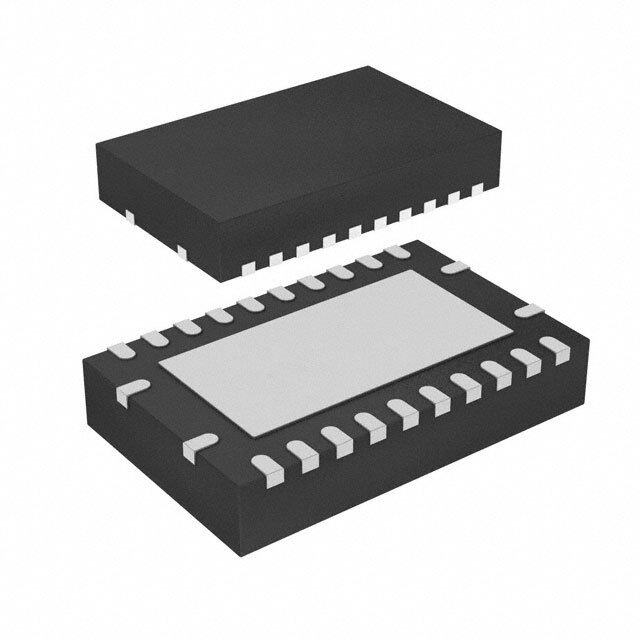
| 封装 | Tube |
| 封装/外壳 | 8-TSSOP,8-MSOP(0.118",3.00mm 宽) |
| 封装/箱体 | MSOP-8 |
| 工作温度 | -40°C ~ 125°C |
| 工作电源电压 | 3 V to 5.5 V |
| 工作电源电流 | 2.8 mA |
| 工厂包装数量 | 100 |
| 开关频率 | 1 MHz |
| 最大工作温度 | + 125 C |
| 最小工作温度 | - 40 C |
| 标准包装 | 100 |
| 电压-电源 | 3 V ~ 5.5 V |
| 类型 | Current Mode PWM Controllers |
| 输出数 | 1 |
| 输出端数量 | 1 Output |
| 配用 | /product-detail/zh/MCP1630DM-LED2/MCP1630DM-LED2-ND/1680065/product-detail/zh/MCP1630RD-NMC1/MCP1630RD-NMC1-ND/1616615/product-detail/zh/MCP1630RD-DDBK3/MCP1630RD-DDBK3-ND/1616614/product-detail/zh/MCP1630DM-DDBK4/MCP1630DM-DDBK4-ND/1616613/product-detail/zh/MCP1630DM-DDBS2/MCP1630DM-DDBS2-ND/1222993/product-detail/zh/MCP1630DM-DDBS1/MCP1630DM-DDBS1-ND/1222991/product-detail/zh/MCP1630DM-NMC1/MCP1630DM-NMC1-ND/735946 |
| 降压 | 是 |
| 隔离式 | 是 |
| 频率-最大值 | 1MHz |


- 商务部:美国ITC正式对集成电路等产品启动337调查
- 曝三星4nm工艺存在良率问题 高通将骁龙8 Gen1或转产台积电
- 太阳诱电将投资9.5亿元在常州建新厂生产MLCC 预计2023年完工
- 英特尔发布欧洲新工厂建设计划 深化IDM 2.0 战略
- 台积电先进制程称霸业界 有大客户加持明年业绩稳了
- 达到5530亿美元!SIA预计今年全球半导体销售额将创下新高
- 英特尔拟将自动驾驶子公司Mobileye上市 估值或超500亿美元
- 三星加码芯片和SET,合并消费电子和移动部门,撤换高东真等 CEO
- 三星电子宣布重大人事变动 还合并消费电子和移动部门
- 海关总署:前11个月进口集成电路产品价值2.52万亿元 增长14.8%


PDF Datasheet 数据手册内容提取
MCP1630/MCP1630V High-Speed, Microcontroller-Adaptable, Pulse Width Modulator Features Description • High-Speed PWM Operation (12ns Current The MCP1630/V is a high-speed Pulse Width Modula- Sense to Output Delay) tor (PWM) used to develop intelligent power systems. • Operating Temperature Range: When used with a microcontroller unit (MCU), the MCP1630/V will control the power system duty cycle to - -40°C to +125°C provide output voltage or current regulation. The MCU • Precise Peak Current Limit (±5%) (MCP1630) can be used to adjust output voltage or current, switch- • Voltage Mode and Average Current Mode Control ing frequency, maximum duty cycle and other features (MCP1630V) that make the power system more intelligent. • CMOS Output Driver (drives MOSFET driver or Typical applications include smart battery chargers, low-side N-channel MOSFET directly) intelligent power systems, brick dc/dc converters, ac • External Oscillator Input power-factor correction, multiple output power supplies, (from PIC® Microcontroller (MCU)) multi-phase power supplies and more. • External Voltage Reference Input (for adjustable The MCP1630/V inputs were developed to be easily voltage or current output application) attached to the I/O of a MCU. The MCU supplies the • Peak Current Mode Operation > 1MHz oscillator and reference to the MCP1630/V to provide • Low Operating Current:2.8mA (typ.) the most flexible and adaptable power system. The • Fast Output Rise and Fall Times: 5.9ns and power system switching frequency and maximum duty 6.2ns cycle are set using the I/O of the MCU. The reference • Undervoltage Lockout (UVLO) Protection input can be external, a D/A Converter (DAC) output or as simple as an I/O output from the MCU. This enables • Output Short Circuit Protection the power system to adapt to many external signals • Overtemperature Protection and variables in order to optimize performance and Applications facilitate calibration. When operating in Current mode, a precise limit is set • Intelligent Power Systems on the peak current. With the fast comparator speed • Smart Battery Charger Applications (typically 12ns), the MCP1630 is capable of providing a • Multiple Output/Multiple Phase Converters tight limit on the maximum switch current over a wide • Output Voltage Calibration input voltage range when compared to other high-speed • AC Power Factor Correction PWM controllers. • VID Capability (programmed and calibrated by For Voltage mode or Average Current mode PIC® microcontroller) applications, the MCP1630V provides a larger range for • Buck/Boost/Buck-Boost/SEPIC/Flyback/Isolated the external ramp voltage. Converters Additional protection features include: UVLO, • Parallel Power Supplies overtemperature and overcurrent. Related Literature Package Type • “MCP1630 NiMH Demo Board User’s Guide”, Microchip Technology Inc., DS51505, 2004 8-Lead DFN 8-Lead MSOP • “MCP1630 Low-Cost Li-Ion Battery Charger (2mm x 3mm) User’s Guide”, Microchip Technology Inc., DS51555, 2005 COMP 1 8 VREF COMP 1 8 VREF • “MCP1630 Li-Ion Multi-Bay Battery Charger FB 2 7 VIN FB 2 7 VIN User’s Guide”, Microchip Technology Inc., CS 3 6 VEXT CS 3 6 VEXT DS51515, 2005 OSC IN 4 5 GND OSC IN 4 5 GND • “MCP1630 Dual Buck Demo Board User’s Guide”, Microchip Technology Inc., DS51531, 2005 2004-2013 Microchip Technology Inc. DS21896C-page 1
MCP1630/MCP1630V Functional Block Diagram – MCP1630 MCP1630 High-Speed PWM VIN VIN Overtemperature 0.1µA UVLO V OSC IN EXT Note S GND VIN Q 0.1µA 100k CS + Q R COMP Comp – V IN Latch Truth Table FB – S R Q V EA REF + 2R 0 0 Qn R 0 1 1 1 0 0 2.7V Clamp 1 1 1 Note: During overtemperature, V driver is high-impedance. EXT DS21896C-page 2 2004-2013 Microchip Technology Inc.
MCP1630/MCP1630V Functional Block Diagram – MCP1630V MCP1630V High-Speed PWM VIN VIN Overtemperature 0.1µA UVLO V OSC IN EXT Note S GND VIN Q 0.1µA 100k CS + Q R COMP Comp – V IN Latch Truth Table FB – S R Q V EA REF + 0 0 Qn 0 1 1 1 0 0 2.7V Clamp 1 1 1 Note: During overtemperature, V driver is high-impedance. EXT 2004-2013 Microchip Technology Inc. DS21896C-page 3
MCP1630/MCP1630V Typical Application Circuit – MCP1630 MCP1630 NiMH Battery Charger and Fuel Gauge Application Diagram CC +V BATT +8V to +15V Input Voltage SEPIC Converter 4 NiMH Cells +5V Bias Cin C OUT MCP1630 1:1 V 5.7V IN IBATT N-channel COMP V EXT MOSFET FB OSC IN CS I SW VREF GND +V BATT +5V Bias + 3V 0V PIC16LF818 PWM OUT V DD MCP1700 3.0V V DD A/D SOT23 1/2 MCP6042 + V DD I2C™ To System A/D + 1/2 MCP6042 DS21896C-page 4 2004-2013 Microchip Technology Inc.
MCP1630/MCP1630V Typical Application Circuit - MCP1630V Bidirectional Power Converter/Battery Charger for 4-Series Cell Li-Ion Batteries 4-Cell Li-Ion Bidirectional Buck/Boost Battery Pack Boost Buck Battery Protection Buck Switches Switch L + Fuse Boost DVoClt aBgues CIN+ Switch +COUT PS501+VBATT – SMBus Battery Protection Sync. FET M aonndit o r -VBATT VSENSE Driver GND RSENSE 0V to 2.7V ISENSE MCP1630V CompVREF +2.5 VREF FB VIN CS VEXT Charge Current Loop OSC GND (1/2) MCP6021 +DC Bus VREF + (1/2) MCP6021 – + – PIC16F88 DC bus Voltage Loop SMBus Filter IREF Voltage (PWM) + – (1/2) MCP6021 2004-2013 Microchip Technology Inc. DS21896C-page 5
MCP1630/MCP1630V 1.0 ELECTRICAL † Notice: Stresses above those listed under “Maximum Ratings” may cause permanent damage to the device. This is CHARACTERISTICS a stress rating only and functional operation of the device at those or any other conditions above those indicated in the Absolute Maximum Ratings † operational listings of this specification is not implied. Exposure to maximum rating conditions for extended periods VDD...................................................................................6.0V may affect device reliability. Maximum Voltage on Any Pin ..(V - 0.3)V to (V + 0.3)V GND IN V Short Circuit Current...........................Internally Limited EXT Storage temperature.....................................-65°C to +150°C Maximum Junction Temperature, T ...........................+150°C J Continuous Operating Temperature Range..-40°C to +125°C ESD protection on all pins, HBM3kV AC/DC CHARACTERISTICS AC/ Electrical Specifications: Unless otherwise noted, V = 3.0V to 5.5V, F = 1MHz with 10% Duty Cycle, C = 0.1µF, IN OSC IN V for typical values=5.0V, T =-40°C to +125°C. IN A Parameters Sym Min Typ Max Units Conditions Input Voltage Input Operating Voltage V 3.0 — 5.5 V IN Input Quiescent Current I(V ) — 2.8 4.5 mA I =0mA, F =0Hz IN EXT OSC IN Oscillator Input External Oscillator Range F — — 1 MHz Note1 OSC Min. Oscillator High Time T — 10 ns OH_MIN Min. Oscillator Low Time T OL_MIN Oscillator Rise Time T 0.01 — 10 µs Note2 RISE Oscillator Fall Time T 0.01 — 10 µs Note2 FALL Oscillator Input Voltage Low V — — 0.8 V L Oscillator Input Voltage High V 2.0 — — V H Oscillator Input Capacitance C 5 pf OSC External Reference Input Reference Voltage Input V 0 — V V Note2, Note3 REF IN Error Amplifier Input Offset Voltage V -4 0.1 +4 mV OS Error Amplifier PSRR PSRR 80 99 — dB V =3.0V to 5.0V, V =1.2V IN CM Common Mode Input Range V GND-0.3 — V V Note2, Note3 CM IN Common Mode Rejection Ratio — 80 — dB V =5V, V =0V to 2.5V IN CM Open-loop Voltage Gain A 85 95 — dB R =5k to V /2, 100mV < V VOL L IN EAOUT < V - 100mV, V =1.2V IN CM Low-level Output V — 25 GND + 50 mV RL=5k to V /2 OL IN Gain Bandwidth Product GBWP — 3.5 — MHz V =5V IN Error Amplifier Sink Current I 5 11 — mA V =5V, V =1.2V, V =1.4V, SINK IN REF FB V =2.0V COMP Error Amplifier Source Current I -2 -9 — mA V =5V, V =1.2V, V =1.0V, SOURCE IN REF FB V =2.0V, Absolute Value COMP Note 1: Capable of higher frequency operation depending on minimum and maximum duty cycles needed. 2: External oscillator input (OSC IN) rise and fall times between 10ns and 10µs used for characterization testing. Signal levels between 0.8V and 2.0V with rise and fall times measured between 10% and 90% of maximum and minimum values. Not production tested. 3: The reference input of the internal amplifier is capable of rail-to-rail operation. DS21896C-page 6 2004-2013 Microchip Technology Inc.
MCP1630/MCP1630V AC/DC CHARACTERISTICS (CONTINUED) Electrical Specifications: Unless otherwise noted, V = 3.0V to 5.5V, F = 1MHz with 10% Duty Cycle, C = 0.1µF, IN OSC IN V for typical values=5.0V, T =-40°C to +125°C. IN A Parameters Sym Min Typ Max Units Conditions Current Sense Input Maximum Current Sense Signal V 0.85 0.9 0.95 V Set by maximum error amplifier CS_MAX MCP1630 clamp voltage, divided by 3. Delay From CS to V T — 12 25 ns EXT CS_VEXT MCP1630 Maximum Current Sense Signal V 2.55 2.7 2.85 V V > 4.25V CS_MAX IN MCP1630V Maximum CS input range limited by comparator input common mode range. V =V -1.4V CS_MAX IN Delay From CS to V T — 17.5 35 ns EXT CS_VEXT MCP1630V Minimum Duty Cycle DC — — 0 % V =V +0.1V, MIN FB REF V =GND CS Current Sense Input Bias Current I — -0.1 — µA V =5V CS_B IN Internal Driver R P-channel R — 10 30 DSON DSon_P R N-channel R — 7 30 DSON DSon_N V Rise Time T — 5.9 18 ns C =100pF EXT RISE L Typical for V =3V IN V Fall Time T — 6.2 18 ns C =100pF EXT FALL L Typical for V =3V IN Protection Features Under Voltage Lockout UVLO 2.7 — 3.0 V V falling, V low state when in IN EXT UVLO Under Voltage Lockout Hysteresis UVLO 50 75 150 mV HYS Thermal Shutdown T — 150 — °C SHD Thermal Shutdown Hysteresis T — 18 — °C SHD_HYS Note 1: Capable of higher frequency operation depending on minimum and maximum duty cycles needed. 2: External oscillator input (OSC IN) rise and fall times between 10ns and 10µs used for characterization testing. Signal levels between 0.8V and 2.0V with rise and fall times measured between 10% and 90% of maximum and minimum values. Not production tested. 3: The reference input of the internal amplifier is capable of rail-to-rail operation. TEMPERATURE SPECIFICATIONS Electrical Specifications: V = 3.0V to 5.5V, F = 1MHz with 10% Duty Cycle, C = 0.1µF. T =-40°C to +125°C. IN OSC IN A Parameters Sym Min Typ Max Units Conditions Temperature Ranges Operating Junction Temperature Range T -40 — +125 °C Steady state A Storage Temperature Range T -65 — +150 °C A Maximum Junction Temperature T — — +150 °C Transient J Thermal Package Resistances Thermal Resistance, 8L-DFN — 50.8 — °C/W Typical 4-layer board with two JA (2mm x 3mm) interconnecting vias Thermal Resistance, 8L-MSOP — 208 — °C/W Typical 4-layer board JA 2004-2013 Microchip Technology Inc. DS21896C-page 7
MCP1630/MCP1630V 2.0 TYPICAL PERFORMANCE CURVES Note: The graphs and tables provided following this note are a statistical summary based on a limited number of samples and are provided for informational purposes only. The performance characteristics listed herein are not tested or guaranteed. In some graphs or tables, the data presented may be outside the specified operating range (e.g., outside specified power supply range) and therefore outside the warranted range. Note: Unless otherwise noted, V = 3.0V to 5.5V, F = 1MHz with 10% Duty Cycle, C = 0.1µF, V for typical IN OSC IN IN values=5.0V, T =-40°C to +125°C. A nt Current (mA) 123...52535 FOSC IN = DC TA = - 40°CTA = + T1A2 =5° +C 25°C ut Bias Current pA) 345670000000000 VCM = VIN TA = + 125°C e p( V QuiescIN 0.051 Amplifier In -1210000000 TA = - 40°C TA = + T85A °=C + 25°C 3 5 5 5 4 5 5 5 5 5 5 3.2 3. 3.7 4.2 4. 4.7 5.2 5. 3 3.25 3.5 3.75 4 4.25 4.5 4.75 5 5.25 5.5 Input Voltage (V) Input Voltage (V) FIGURE 2-1: Input Quiescent Current vs. FIGURE 2-4: Error Amplifier Input Bias Input Voltage. Current vs. Input Voltage. 4.5 18 mA) 4 FOSC IN = 1 MHz TA = + 125°C mA) 16 nt ( 3.5 nt ( 14 TA = - 40°C nt Curre 2.235 TA = - 40°C TA = + 25°C nk Curre 11028 TA = + 25°C QuiesceN 01..155 mplifier Si 246 TA = + 125°C VI 0 A 0 3 5 5 5 4 5 5 5 5 5 5 3 5 5 5 4 5 5 5 5 5 5 3.2 3. 3.7 4.2 4. 4.7 5.2 5. 3.2 3. 3.7 4.2 4. 4.7 5.2 5. Input Voltage (V) Input Voltage (V) FIGURE 2-2: Input Quiescent Current vs. FIGURE 2-5: Error Amplifier Sink Current Input Voltage. vs. Input Voltage. 2 250 A) 0 Gain m Amplifier Gain (db) --11----2086420 VRCRLLOOEFAA DD= ==P2 Vh46.7a7 s pkeF 51120050000 Amplifier Phase Shift (degrees) plifier Source Current ( --11----208642 TTTAAA == = ++ - 214520°5°C°CC m -14 -14 0 A 3 5 5 5 4 5 5 5 5 5 5 1 0 10M0000 5M 1 10000M0000 3.2 3. 3.7 4.2 4. 4.7 5.2 5. Frequency (Hz) Input Voltage (V) FIGURE 2-3: Error Amplifier Frequency FIGURE 2-6: Error Amplifier Source Response. Current vs. Input Voltage. DS21896C-page 8 2004-2013 Microchip Technology Inc.
MCP1630/MCP1630V Note: Unless otherwise noted, V = 3.0V to 5.5V, F = 1MHz with 10% Duty Cycle, C = 0.1µF, V for typical IN OSC IN IN values=5.0V, T =-40°C to +125°C. A 10 0.9 9 CL = 100 pF e (ns) 78 TA = + 125°C age (V) 0.899 TA = - 40°C Tim 56 Volt 0.898 TA = + 125°C V Rise EXT 1234 TA = + 25°C TA = - 40°C CS Clamp 00..889967 TA = + 25°C 0 0.895 3 5 5 5 4 5 5 5 5 5 5 3 5 5 5 4 5 5 5 5 5 5 3.2 3. 3.7 4.2 4. 4.7 5.2 5. 3.2 3. 3.7 4.2 4. 4.7 5.2 5. Input Voltage (V) Input Voltage (V) FIGURE 2-7: V Rise Time vs. Input FIGURE 2-10: Current Sense Clamp EXT Voltage. Voltage vs. Input Voltage (MCP1630). 9 2.96 8 CL = 100 pF ns) 7 TA = + 125°C V) 2.94 Turn On Threshold e ( 6 d ( 2.92 V Fall TimEXT 2345 TA = + 25°C TA = - 40°C LO Threshol 22..8980 Turn Off Threshold 1 UV 2.86 0 3 3.25 3.5 3.75 4 4.25 4.5 4.75 5 5.25 5.5 2.84-40 -25 -10 5 20 35 50 65 80 95 110125 Input Voltage (V) Ambient Temperature (°C) FIGURE 2-8: V Fall Time vs. Input FIGURE 2-11: Undervoltage Lockout vs. EXT Voltage. Temperature. 25 N 12 O DS o V delay (ns)EXT 112050 TA = + 25°C TTAA = = + - 14205°C°C put N-Channel R(ohms)10468 TA = + 25°C TAT =A -= 4 +0 °1C25°C S t 5 Out 2 C T X 0 E 0 3 3.25 3.5 3.75 4 4.25 4.5 4.75 5 5.25 5.5 3 3.25 3.5 3.75 4 4.25 4.5 4.75 5 5.25 5.5 Input Voltage (V) Input Voltage (V) FIGURE 2-9: Current Sense to V FIGURE 2-12: EXT Output N-channel EXT Delay vs. Input Voltage (MCP1630). R vs. Input Voltage. DSON 2004-2013 Microchip Technology Inc. DS21896C-page 9
MCP1630/MCP1630V Note: Unless otherwise noted, V = 3.0V to 5.5V, F = 1MHz with 10% Duty Cycle, C = 0.1µF, V for typical IN OSC IN IN values=5.0V, T =-40°C to +125°C. A ON 18 3 CS Common Mode nnel RDS 111246 TA = + 125°C put (V) 2.7 Input RangeTA = +25°C Chams) 10 S In 2.4 T Output P-(Oh 2468 TA = + 25°C TA = - 40°C Maximum C 12..81 X E 0 1.5 3 5 5 5 4 5 5 5 5 5 5 3.2 3. 3.7 4.2 4. 4.7 5.2 5. 3 3.5 4 4.5 5 5.5 Input Voltage (V) Input Voltage (V) FIGURE 2-13: EXT Output P-channel FIGURE 2-16: Current Sense Common R vs. Input Voltage. Mode Input Voltage Range vs. Input Voltage DSON (MCP1630V). ge 0 30 Volta -50 TA = + 125°C ns) 25 TA = +125°C p Input Offset (µV) --115000 TA = + 25°C VCM IN = 0V o V Delay (EXT 112050 TA = -40°C TA = +25°C Am -200 CS t 5 or TA = - 40°C Err -250 0 3 5 5 5 4 5 5 5 5 5 5 3 5 5 5 4 5 5 5 5 5 5 3.2 3. 3.7 4.2 4. 4.7 5.2 5. 3.2 3. 3.7 4.2 4. 4.7 5.2 5. Input Voltage (V) Input Voltage (V) FIGURE 2-14: Error Amplifier Input Offset FIGURE 2-17: Current Sense to V EXT Voltage vs. Input Voltage. Delay vs. Input Voltage (MCP1630V). ge 150 a olt 100 TA = + 125°C V et 50 put Offs(µV) -500 VCM IN = 1.2V n mp I -100 TA = + 25°C A -150 or TA = - 40°C Err -200 3 5 5 5 4 5 5 5 5 5 5 3.2 3. 3.7 4.2 4. 4.7 5.2 5. Input Voltage (V) FIGURE 2-15: Error Amplifier Input Offset Voltage vs. Input Voltage. DS21896C-page 10 2004-2013 Microchip Technology Inc.
MCP1630/MCP1630V 3.0 MCP1630 PIN DESCRIPTIONS The descriptions of the pins are listed in Table3-1. TABLE 3-1: PIN FUNCTION TABLE DFN/MSOP Name Function 1 COMP Error Amplifier Output pin 2 FB Error Amplifier Inverting Input 3 CS Current Sense Input pin (MCP1630) or Voltage Ramp Input pin (MCP1630V) 4 OSC IN Oscillator Input pin 5 GND Circuit Ground pin 6 V External Driver Output pin EXT 7 V Input Bias pin IN 8 V Reference Voltage Input pin REF 3.1 Error Amplifier Output Pin (COMP) low. The high-to-low transition initiates the start of a new cycle. The duty cycle of the OSC input pin deter- COMP is an internal error amplifier output pin. External mines the maximum duty cycle of the power converter. compensation is connected from the FB pin to the For example, if the OSC input is low for 75% of the time COMP pin for control-loop stabilization. An internal and high for 25% of the time, the duty cycle range for voltage clamp is used to limit the maximum COMP pin the power converter is 0% to 75% maximum. voltage to 2.7V (typ.). This clamp is used to set the maximum peak current in the power system switch by 3.5 Ground (GND) setting a maximum limit on the CS input for Peak Current mode control systems. Connect the circuit ground to the GND pin. For most applications, this should be connected to the analog or 3.2 Error Amplifier Inverting Input quiet ground plane. Noise on this ground can affect the (FB) sensitive cycle-by-cycle comparison between the CS input and the error amplifier output. FB is an internal error amplifier inverting input pin. The output (voltage or current) is sensed and fed back to 3.6 External Driver Output Pin (V ) the FB pin for regulation. Inverting or negative EXT feedback is used. V is an external driver output pin, used to determine EXT the power system duty cycle. For high-power or high- 3.3 Current Sensing Input (CS) side drives, this output should be connected to the logic- level input of the MOSFET driver. For low-power, low- CS is the current sense input pin used for cycle-by- side applications, the V pin can be used to directly cycle control for Peak Current mode converters. The EXT drive the gate of an N-channel MOSFET. MCP1630 is typically used for sensed current applications to reduce the current sense signal, thus 3.7 Input Bias Pin (V ) reducing power dissipation. IN For Voltage mode or Average Current mode V is an input voltage pin. Connect the input voltage IN applications, a ramp is used to compare the error source to the V pin. For normal operation, the voltage IN amplifier output voltage with producing the PWM duty on the V pin should be between +3.0V and +5.5V. A IN cycle. For applications that require higher signal levels, 0.1µF bypass capacitor should be connected between the MCP1630V is used to increase the level from a the V pin and the GND pin. IN maximum of 0.9V (MCP1630) to 2.7V (MCP1630V). The common mode voltage range for the MCP1630V 3.8 Reference Voltage Input (V ) REF CS input is V -1.4V. For normal PWM operation, the IN CS input should be less than or equal to VIN - 1.4V at VREF is an external reference input pin used to regulate all times. the output of the power system. By changing the VREF input, the output (voltage or current) of the power sys- 3.4 Oscillator Input (OSC) tem can be changed. The reference voltage can range from 0V to V (rail-to-rail). IN OSC is an external oscillator input pin. Typically, a microcontroller I/O pin is used to generate the OSC input. When high, the output driver pin (V ) is driven EXT 2004-2013 Microchip Technology Inc. DS21896C-page 11
MCP1630/MCP1630V 4.0 DETAILED DESCRIPTION For Voltage mode or Average Current mode applica- tions that utilize a large signal ramp at the CS input, the 4.1 Device Overview MCP1630V is used to provide more signal (2.7V typ.). The operation of the PWM does not change. The MCP1630 is comprised of a high-speed compara- tor, high-bandwidth amplifier and logic gates that can 4.4 Error Amp/Comparator Current be combined with a PIC MCU to develop an advanced Limit Function programmable power supply. The oscillator and refer- ence voltage inputs are generated by the PIC MCU so The internal amplifier is used to create an error output that switching frequency, maximum duty cycle and out- signal that is determined by the external VREF input and put voltage are programmable. Refer to Figure4-1. the power supply output fed back into the FB pin. The error amplifier output is rail-to-rail and clamped by a 4.2 PWM precision 2.7V. The output of the error amplifier is then divided down 3:1 (MCP1630) and connected to the The V output of the MCP1630/V is determined by EXT inverting input of the high-speed comparator. Since the the output level of the internal high-speed comparator maximum output of the error amplifier is 2.7V, the max- and the level of the external oscillator. When the oscil- imum input to the inverting pin of the high-speed com- lator level is high, the PWM output (V ) is forced low. EXT parator is 0.9V. This sets the peak current limit for the When the external oscillator is low, the PWM output is switching power supply. determined by the output level of the internal high- speed comparator. During UVLO, the V pin is held For the MCP1630V, the maximum error amplifier out- EXT in the low state. During overtemperature operation, the put is still 2.7V. However, the resistor divider is V pin is high-impedance (100k to ground). removed, raising the maximum input signal level at the EXT high-speed comparator inverting input (CS) to 2.7V. 4.3 Normal Cycle by Cycle Control As the output load current demand increases, the error amplifier output increases, causing the inverting input The beginning of a cycle is defined when OSC IN tran- pin of the high-speed comparator to increase. sitions from a high state to a low state. For normal oper- Eventually, the output of the error amplifier will hit the ation, the state of the high-speed comparator output 2.7V clamp, limiting the input of the high-speed com- (R) is low and the Q output of the latch is low. On the parator to 0.9V max (MCP1630). Even if the FB input OSC IN high-to-low transition, the S and R inputs to the continues to decrease (calling for more current), the high-speed latch are both low and the Q output will inverting input is limited to 0.9V. By limiting the inverting remain unchanged (low). The output of the OR gate input to 0.9V, the current-sense input (CS) is limited to (V ) will transition from a high state to a low state, DRIVE 0.9V, thus limiting the output current of the power turning on the internal P-channel drive transistor in the supply. output stage of the PWM. This will change the PWM output (V ) from a low state to a high state, turning For Voltage mode control, the error amplifier output will EXT on the power-train external switch and ramping current increase as input voltage decreases. A voltage ramp is in the power-train magnetic device. used instead of sensed inductor current at the CS input of the MCP1630V. The 3:1 internal error amplifier out- The sensed current in the magnetic device is fed into put resistor divider is removed in the MCP1630V option the CS input (shown as a ramp) and increases linearly. to increase the maximum signal level input to 2.7V Once the sensed current ramp (MCP1630) reaches the (typ.). same voltage level as 1/3 of the EA output, the compar- ator output (R) changes states (low-to-high) and resets 4.5 0% Duty Cycle Operation the PWM latch. The Q output transitions from a low state to a high state, turning on the N-channel MOSFET The duty cycle of the V output is capable of reach- EXT in the output stage, which turns off the VEXT drive to the ing 0% when the FB pin is held higher than the VREF pin external MOSFET driver terminating the duty cycle. (inverting error amplifier). This is accomplished by the The OSC IN will transition from a low state to a high rail-to-rail output capability of the error amplifier and the state while the VEXT pin remains unchanged. If the CS offset voltage of the high-speed comparator. The mini- input ramp had never reached the same level as 1/3 of mum error amplifier output voltage, divided by three, is the error amplifier output, the low-to-high transition on less than the offset voltage of the high-speed compar- OSC IN would terminate the duty cycle and this would ator. In the case where the output voltage of the con- be considered maximum duty cycle. In either case, verter is above the desired regulation point, the FB while OSC IN is high, the VEXT drive pin is low, turning input will be above the VREF input and the error ampli- off the external power-train switch. The next cycle will fier will be pulled to the bottom rail (GND). This low start on the transition of the OSC IN pin from a high voltage is divided down 3:1 by the 2R and 1R resistor state to a low state. (MCP1630) and connected to the input of the high- speed comparator. This voltage will be low enough so that there is no triggering of the comparator, allowing narrow pulse widths at V . EXT DS21896C-page 12 2004-2013 Microchip Technology Inc.
MCP1630/MCP1630V 4.6 Undervoltage Lockout (UVLO) 4.7 Overtemperature Protection When the input voltage (V ) is less than the UVLO To protect the V output if shorted to V or GND, the IN EXT IN threshold, the V is held in the low state. This will MCP1630/V V output will be high-impedance if the EXT EXT ensure that, if the voltage is not adequate to operate junction temperature is above the thermal shutdown the MCP1630/V, the main power supply switch will be threshold. There is an internal 100k pull-down resis- held in the off state. When the UVLO threshold is tor connected from V to ground to provide some EXT exceeded, there is some hysteresis in the input voltage pull-down during overtemperature conditions. The prior to the UVLO off threshold being reached. The protection is set to 150°C (typ.), with a hysteresis of typical hysteresis is 75mV. Typically, the MCP1630 will 18°C. not start operating until the input voltage at V is IN between 3.0V and 3.1V. 2004-2013 Microchip Technology Inc. DS21896C-page 13
MCP1630/MCP1630V MCP1630 High-Speed PWM Timing Diagram OSC IN S COMP CS R Q V DRIVE V EXT V IN V IN Overtemperature 0.1µA UVLO V OSC IN EXT Note S GND VIN Q 0.1µA 100k CS + Q R COMP Comp – Latch Truth Table V IN S R Q FB – 0 0 Qn V EA REF + 2R 0 1 1 R 1 0 0 1 1 1 2.7V Clamp Note: During overtemperature, V driver is high-impedance. EXT FIGURE 4-1: Cycle-by-Cycle Timing Diagram (MCP1630). DS21896C-page 14 2004-2013 Microchip Technology Inc.
MCP1630/MCP1630V MCP1630V High-Speed PWM Timing Diagram OSC IN S COMP CS R Q V DRIVE V EXT V IN V IN Overtemperature 0.1µA UVLO V OSC IN EXT V DRIVE Note S GND VIN Q 0.1µA 100k CS + Q R COMP Comp – Latch Truth Table V IN S R Q FB – 0 0 Qn V EA REF + 0 1 1 1 0 0 1 1 1 2.7V Clamp Note: During overtemperature, V driver is high-impedance. EXT FIGURE 4-2: Cycle-by-Cycle Timing Diagram (MCP1630V). 2004-2013 Microchip Technology Inc. DS21896C-page 15
MCP1630/MCP1630V 5.0 APPLICATION 5.3 Bidirectional Power Converter CIRCUITS/ISSUES A bidirectional Li-Ion charger/buck regulator is shown in the “Typical Application Circuit” of the this data 5.1 Typical Applications sheet. In this example, a synchronous, bidirectional power converter example is shown using the The MCP1630/V high-speed PWM can be used for any MCP1630V. In this application, when the ac-dc input circuit topology and power-train application when power is present, the bidirectional power converter is combined with a microcontroller. Intelligent, cost- used to charge 4-series Li-Ion batteries by boosting the effective power systems can be developed for applica- input voltage. When ac-dc power is removed, the tions that require multiple outputs, multiple phases, bidirectional power converter bucks the battery voltage adjustable outputs, temperature monitoring and down to provide a dc bus for system power. By using calibration. this method, a single power train is capable of charging 4-series cell Li-Ion batteries and efficiently converting 5.2 NiMH Battery Charger Application the battery voltage down to a low, usable voltage. A typical NiMH battery charger application is shown in 5.4 Multiple Output Converters the “Typical Application Circuit – MCP1630” of this data sheet. In that example, a Single-Ended Primary By using additional MCP1630 devices, multiple output Inductive Converter (SEPIC) is used to provide a converters can be developed using a single MCU. If a constant charge current to the series-connected two-output converter is desired, the MCU can provide batteries. The MCP1630 is used to regulate the charge two PWM outputs that are phased 180° apart. This will current by monitoring the current through the battery reduce the input ripple current to the source and sense resistor and providing the proper pulse width. eliminate beat frequencies. The PIC16F818 monitors the battery voltage to provide a termination to the charge current. Additional features (trickle charge, fast charge, overvoltage protection, etc.) can be added to the system using the programma- bility of the microcontroller and the flexibility of the MCP1630. DS21896C-page 16 2004-2013 Microchip Technology Inc.
MCP1630/MCP1630V 6.0 PACKAGING INFORMATION 6.1 Package Marking Information Example: 1630E 522256 8-Lead MSOP XXXXX YWWNNN Example: 1630VE 522256 8-Lead DFN (2mm x 3mm) Example: XXX ABC YWW 522 NN 25 For DFN samples, contact your Microchip Sales Office for availability.. Legend: XX...X Customer-specific information Y Year code (last digit of calendar year) YY Year code (last 2 digits of calendar year) WW Week code (week of January 1 is week ‘01’) NNN Alphanumeric traceability code e3 Pb-free JEDEC designator for Matte Tin (Sn) * This package is Pb-free. The Pb-free JEDEC designator ( e 3 ) can be found on the outer packaging for this package. Note: In the event the full Microchip part number cannot be marked on one line, it will be carried over to the next line, thus limiting the number of available characters for customer-specific information. 2004-2013 Microchip Technology Inc. DS21896C-page 17
MCP1630/MCP1630V 8-Lead Plastic Micro Small Outline Package (MS) (MSOP) Note: For the most current package drawings, please see the Microchip Packaging Specification located at http://www.microchip.com/packaging E E1 p D 2 B n 1 α A A2 c φ A1 (F) L β Units INCHES MILLIMETERS* Dimension Limits MIN NOM MAX MIN NOM MAX Number of Pins n 8 8 Pitch p .026 BSC 0.65 BSC Overall Height A - - .043 - - 1.10 Molded Package Thickness A2 .030 .033 .037 0.75 0.85 0.95 Standoff A1 .000 - .006 0.00 - 0.15 Overall Width E .193 TYP. 4.90 BSC Molded Package Width E1 .118 BSC 3.00 BSC Overall Length D .118 BSC 3.00 BSC Foot Length L .016 .024 .031 0.40 0.60 0.80 Footprint (Reference) F .037 REF 0.95 REF Foot Angle φ 0° - 8° 0° - 8° Lead Thickness c .003 .006 .009 0.08 - 0.23 Lead Width B .009 .012 .016 0.22 - 0.40 Mold Draft Angle Top α 5° - 15° 5° - 15° Mold Draft Angle Bottom β 5° - 15° 5° - 15° *Controlling Parameter Notes: Dimensions D and E1 do not include mold flash or protrusions. Mold flash or protrusions shall not exceed .010" (0.254mm) per side. JEDEC Equivalent: MO-187 Drawing No. C04-111 DS21896C-page 18 2004-2013 Microchip Technology Inc.
MCP1630/MCP1630V 8-Lead Plastic Dual Flat No Lead Package (MC) 2x3x0.9 mm Body (DFN) – Saw Singulated Note: For the most current package drawings, please see the Microchip Packaging Specification located at http://www.microchip.com/packaging For DFN samples, contact your Microchip Sales Office for availability.. p D b n L E E2 EXPOSED METAL 2 1 PIN 1 PAD ID INDEX D2 AREA (NOTE 2) TOP VIEW BOTTOM VIEW A A3 A1 EXPOSED TIE BAR (NOTE 1) Units INCHES MILLIMETERS* Dimension Limits MIN NOM MAX MIN NOM MAX Number of Pins n 8 8 Pitch p .020 BSC 0.50 BSC Overall Height A .031 .035 .039 0.80 0.90 1.00 Standoff A1 .000 .001 .002 0.00 0.02 0.05 Contact Thickness A3 .008 REF. 0.20 REF. Overall Length D .079 BSC 2.00 BSC Exposed Pad Length (Note 3) D2 .055 .065 .067 1.39 1.65 1.70 Overall Width E .118 BSC 3.00 BSC Exposed Pad Width (Note 3) E2 .047 .059 .061 1.20 1.50 1.55 Contact Width b .008 .010 .012 0.20 0.25 0.30 Contact Length L .012 .016 .020 0.30 0.40 0.50 *Controlling Parameter Notes: 1. BSC: Basic Dimension. Theoretically exact value shown without tolerances. See ASME Y14.5M 2. REF: Reference Dimension, usually without tolerance, for information purposes only. See ASME Y14.5M Exposed pad varies according to die attach paddle size. Package may have one or more exposed tie bars at ends. Pin 1 visual index feature may vary, but must be located within the hatched area. JEDEC equivalent: M0-229 Drawing No. C04-123, Revised 05-05-05 2004-2013 Microchip Technology Inc. DS21896C-page 19
MCP1630/MCP1630V NOTES: DS21896C-page 20 2004-2013 Microchip Technology Inc.
MCP1630/MCP1630V APPENDIX A: REVISION HISTORY Revision C (January 2013) • Added a note to each package outline drawing. Revision B (June 2005) The following is the list of modifications: 1. Added MCP1630V device information throughout data sheet 2. Added DFN package information throughout data sheet. 3. Added Appendix A: Revision History. Revision A (June 2004) • Original Release of this Document. 2004-2013 Microchip Technology Inc. DS21896C-page 21
MCP1630/MCP1630V NOTES: l DS21896C-page 22 2004-2013 Microchip Technology Inc.
MCP1630/MCP1630V PRODUCT IDENTIFICATION SYSTEM To order or obtain information, e.g., on pricing or delivery, refer to the factory or the listed sales office. PART NO. X /XX Examples: a) MCP1630-E/MS: Extended Temperature, Device Temperature Package 8LD MSOP package. Range b) MCP1630T-E/MS: Tape and Reel Extended Temperature, 8LD MSOP package. c) MCP1630-E/MC: Extended Temperature, Device: MCP1630: High-Speed, Microcontroller-Adaptable, 8LD DFN package. PWM MCP1630T: High-Speed, Microcontroller-Adaptable, PWM (Tape and Reel) a) MCP1630V-E/MS: Extended Temperature, 8LD MSOP package. Temperature Range: E = -40°C to +125°C b) MCP1630VT-E/MS:Tape and Reel Extended Temperature, 8LD MSOP package. Package: MC *= Dual Flat, No Lead (2x3mm Body), 8-lead c) MCP1630V-E/MC: Extended Temperature, MS = Plastic MSOP, 8-lead 8LD DFN package. * For DFN samples, contact your Microchip Sales Office for availability. 2004-2013 Microchip Technology Inc. DS21896C-page 23
MCP1630/MCP1630V NOTES: DS21896C-page 24 2004-2013 Microchip Technology Inc.
Note the following details of the code protection feature on Microchip devices: • Microchip products meet the specification contained in their particular Microchip Data Sheet. • Microchip believes that its family of products is one of the most secure families of its kind on the market today, when used in the intended manner and under normal conditions. • There are dishonest and possibly illegal methods used to breach the code protection feature. All of these methods, to our knowledge, require using the Microchip products in a manner outside the operating specifications contained in Microchip’s Data Sheets. Most likely, the person doing so is engaged in theft of intellectual property. • Microchip is willing to work with the customer who is concerned about the integrity of their code. • Neither Microchip nor any other semiconductor manufacturer can guarantee the security of their code. Code protection does not mean that we are guaranteeing the product as “unbreakable.” Code protection is constantly evolving. We at Microchip are committed to continuously improving the code protection features of our products. Attempts to break Microchip’s code protection feature may be a violation of the Digital Millennium Copyright Act. If such acts allow unauthorized access to your software or other copyrighted work, you may have a right to sue for relief under that Act. Information contained in this publication regarding device Trademarks applications and the like is provided only for your convenience The Microchip name and logo, the Microchip logo, dsPIC, and may be superseded by updates. It is your responsibility to FlashFlex, KEELOQ, KEELOQ logo, MPLAB, PIC, PICmicro, ensure that your application meets with your specifications. PICSTART, PIC32 logo, rfPIC, SST, SST Logo, SuperFlash MICROCHIP MAKES NO REPRESENTATIONS OR and UNI/O are registered trademarks of Microchip Technology WARRANTIES OF ANY KIND WHETHER EXPRESS OR Incorporated in the U.S.A. and other countries. IMPLIED, WRITTEN OR ORAL, STATUTORY OR OTHERWISE, RELATED TO THE INFORMATION, FilterLab, Hampshire, HI-TECH C, Linear Active Thermistor, INCLUDING BUT NOT LIMITED TO ITS CONDITION, MTP, SEEVAL and The Embedded Control Solutions QUALITY, PERFORMANCE, MERCHANTABILITY OR Company are registered trademarks of Microchip Technology FITNESS FOR PURPOSE. Microchip disclaims all liability Incorporated in the U.S.A. arising from this information and its use. Use of Microchip Silicon Storage Technology is a registered trademark of devices in life support and/or safety applications is entirely at Microchip Technology Inc. in other countries. the buyer’s risk, and the buyer agrees to defend, indemnify and Analog-for-the-Digital Age, Application Maestro, BodyCom, hold harmless Microchip from any and all damages, claims, chipKIT, chipKIT logo, CodeGuard, dsPICDEM, suits, or expenses resulting from such use. No licenses are dsPICDEM.net, dsPICworks, dsSPEAK, ECAN, conveyed, implicitly or otherwise, under any Microchip ECONOMONITOR, FanSense, HI-TIDE, In-Circuit Serial intellectual property rights. Programming, ICSP, Mindi, MiWi, MPASM, MPF, MPLAB Certified logo, MPLIB, MPLINK, mTouch, Omniscient Code Generation, PICC, PICC-18, PICDEM, PICDEM.net, PICkit, PICtail, REAL ICE, rfLAB, Select Mode, SQI, Serial Quad I/O, Total Endurance, TSHARC, UniWinDriver, WiperLock, ZENA and Z-Scale are trademarks of Microchip Technology Incorporated in the U.S.A. and other countries. SQTP is a service mark of Microchip Technology Incorporated in the U.S.A. GestIC and ULPP are registered trademarks of Microchip Technology Germany II GmbH & Co. & KG, a subsidiary of Microchip Technology Inc., in other countries. All other trademarks mentioned herein are property of their respective companies. © 2004-2013, Microchip Technology Incorporated, Printed in the U.S.A., All Rights Reserved. Printed on recycled paper. ISBN: 9781620769140 QUALITY MANAGEMENT SYSTEM Microchip received ISO/TS-16949:2009 certification for its worldwide headquarters, design and wafer fabrication facilities in Chandler and CERTIFIED BY DNV Tempe, Arizona; Gresham, Oregon and design centers in California and India. The Company’s quality system processes and procedures == ISO/TS 16949 == are for its PIC® MCUs and dsPIC® DSCs, KEELOQ® code hopping devices, Serial EEPROMs, microperipherals, nonvolatile memory and analog products. In addition, Microchip’s quality system for the design and manufacture of development systems is ISO 9001:2000 certified. 2004-2013 Microchip Technology Inc. DS21896C-page 25
Worldwide Sales and Service AMERICAS ASIA/PACIFIC ASIA/PACIFIC EUROPE Corporate Office Asia Pacific Office India - Bangalore Austria - Wels 2355 West Chandler Blvd. Suites 3707-14, 37th Floor Tel: 91-80-3090-4444 Tel: 43-7242-2244-39 Chandler, AZ 85224-6199 Tower 6, The Gateway Fax: 91-80-3090-4123 Fax: 43-7242-2244-393 Tel: 480-792-7200 Harbour City, Kowloon India - New Delhi Denmark - Copenhagen Fax: 480-792-7277 Hong Kong Tel: 91-11-4160-8631 Tel: 45-4450-2828 Technical Support: Tel: 852-2401-1200 Fax: 91-11-4160-8632 Fax: 45-4485-2829 http://www.microchip.com/ support Fax: 852-2401-3431 India - Pune France - Paris Web Address: Australia - Sydney Tel: 91-20-2566-1512 Tel: 33-1-69-53-63-20 www.microchip.com Tel: 61-2-9868-6733 Fax: 91-20-2566-1513 Fax: 33-1-69-30-90-79 Atlanta Fax: 61-2-9868-6755 Japan - Osaka Germany - Munich Duluth, GA China - Beijing Tel: 81-6-6152-7160 Tel: 49-89-627-144-0 Tel: 86-10-8569-7000 Fax: 49-89-627-144-44 Tel: 678-957-9614 Fax: 81-6-6152-9310 Fax: 678-957-1455 Fax: 86-10-8528-2104 Japan - Tokyo Italy - Milan China - Chengdu Tel: 39-0331-742611 Boston Tel: 81-3-6880- 3770 Tel: 86-28-8665-5511 Fax: 39-0331-466781 Westborough, MA Fax: 81-3-6880-3771 Tel: 774-760-0087 Fax: 86-28-8665-7889 Korea - Daegu Netherlands - Drunen Fax: 774-760-0088 China - Chongqing Tel: 82-53-744-4301 Tel: 31-416-690399 Chicago Tel: 86-23-8980-9588 Fax: 82-53-744-4302 Fax: 31-416-690340 Itasca, IL Fax: 86-23-8980-9500 Korea - Seoul Spain - Madrid Tel: 630-285-0071 China - Hangzhou Tel: 82-2-554-7200 Tel: 34-91-708-08-90 Fax: 630-285-0075 Tel: 86-571-2819-3187 Fax: 82-2-558-5932 or Fax: 34-91-708-08-91 Cleveland Fax: 86-571-2819-3189 82-2-558-5934 UK - Wokingham Independence, OH China - Hong Kong SAR Malaysia - Kuala Lumpur Tel: 44-118-921-5869 Tel: 216-447-0464 Tel: 852-2943-5100 Tel: 60-3-6201-9857 Fax: 44-118-921-5820 Fax: 216-447-0643 Fax: 852-2401-3431 Fax: 60-3-6201-9859 Dallas China - Nanjing Malaysia - Penang Addison, TX Tel: 86-25-8473-2460 Tel: 60-4-227-8870 Tel: 972-818-7423 Fax: 86-25-8473-2470 Fax: 60-4-227-4068 Fax: 972-818-2924 China - Qingdao Philippines - Manila Detroit Tel: 86-532-8502-7355 Tel: 63-2-634-9065 Farmington Hills, MI Fax: 86-532-8502-7205 Fax: 63-2-634-9069 Tel: 248-538-2250 Fax: 248-538-2260 China - Shanghai Singapore Tel: 86-21-5407-5533 Tel: 65-6334-8870 Indianapolis Fax: 86-21-5407-5066 Fax: 65-6334-8850 Noblesville, IN Tel: 317-773-8323 China - Shenyang Taiwan - Hsin Chu Fax: 317-773-5453 Tel: 86-24-2334-2829 Tel: 886-3-5778-366 Fax: 86-24-2334-2393 Fax: 886-3-5770-955 Los Angeles Mission Viejo, CA China - Shenzhen Taiwan - Kaohsiung Tel: 949-462-9523 Tel: 86-755-8864-2200 Tel: 886-7-213-7828 Fax: 949-462-9608 Fax: 86-755-8203-1760 Fax: 886-7-330-9305 Santa Clara China - Wuhan Taiwan - Taipei Santa Clara, CA Tel: 86-27-5980-5300 Tel: 886-2-2508-8600 Tel: 408-961-6444 Fax: 86-27-5980-5118 Fax: 886-2-2508-0102 Fax: 408-961-6445 China - Xian Thailand - Bangkok Toronto Tel: 86-29-8833-7252 Tel: 66-2-694-1351 Mississauga, Ontario, Fax: 86-29-8833-7256 Fax: 66-2-694-1350 Canada China - Xiamen Tel: 905-673-0699 Tel: 86-592-2388138 Fax: 905-673-6509 Fax: 86-592-2388130 China - Zhuhai Tel: 86-756-3210040 11/29/12 Fax: 86-756-3210049 DS21896C-page 26 2004-2013 Microchip Technology Inc.