ICGOO在线商城 > 集成电路(IC) > PMIC - 监控器 > MCP121T-195I/TT

 Datasheet下载
- 型号: MCP121T-195I/TT
- 制造商: Microchip
- 库位|库存: xxxx|xxxx
- 要求:
| 数量阶梯 | 香港交货 | 国内含税 |
| +xxxx | $xxxx | ¥xxxx |
查看当月历史价格
查看今年历史价格
MCP121T-195I/TT产品简介:
ICGOO电子元器件商城为您提供MCP121T-195I/TT由Microchip设计生产,在icgoo商城现货销售,并且可以通过原厂、代理商等渠道进行代购。 MCP121T-195I/TT价格参考。MicrochipMCP121T-195I/TT封装/规格:PMIC - 监控器, 开路漏极或开路集电极 监控器 1 通道 SOT-23-3。您可以下载MCP121T-195I/TT参考资料、Datasheet数据手册功能说明书,资料中有MCP121T-195I/TT 详细功能的应用电路图电压和使用方法及教程。
| 参数 | 数值 |
| 产品目录 | 集成电路 (IC)半导体 |
| 描述 | IC SUPERVISOR 1.95V LOW SOT-23B监控电路 Open Drain Low |
| 产品分类 | |
| 品牌 | Microchip Technology |
| 产品手册 | |
| 产品图片 |
|
| rohs | 符合RoHS无铅 / 符合限制有害物质指令(RoHS)规范要求 |
| 产品系列 | 电源管理 IC,监控电路,Microchip Technology MCP121T-195I/TT- |
| NumberofInputsMonitored | 1 Input |
| 数据手册 | http://www.microchip.com/mymicrochip/filehandler.aspx?ddocname=en022913http://www.microchip.com/mymicrochip/filehandler.aspx?ddocname=en023833 |
| 产品型号 | MCP121T-195I/TT |
| PCN设计/规格 | http://www.microchip.com/mymicrochip/NotificationDetails.aspx?id=5804&print=view |
| 产品目录页面 | |
| 产品种类 | Supervisors |
| 人工复位 | No Manual Reset |
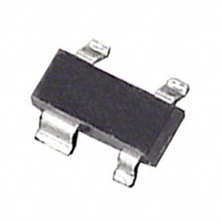
| 供应商器件封装 | SOT-23-3 |
| 其它名称 | MCP121T-195I/TTDKR |
| 包装 | Digi-Reel® |
| 受监控电压数 | 1 |
| 商标 | Microchip Technology |
| 复位 | 低有效 |
| 复位超时 | 最小为 80 ms |
| 安装类型 | 表面贴装 |
| 安装风格 | SMD/SMT |
| 封装 | Reel |
| 封装/外壳 | TO-236-3,SC-59,SOT-23-3 |
| 封装/箱体 | SOT-23-3 |
| 工作温度 | -40°C ~ 85°C |
| 工作电源电流 | 20 uA |
| 工厂包装数量 | 3000 |
| 最大工作温度 | + 85 C |
| 最小工作温度 | - 40 C |
| 标准包装 | 1 |
| 欠电压阈值 | 1.872 V |
| 电压-阈值 | 1.9V |
| 电池备用开关 | No Backup |
| 电源电压-最大 | 5.5 V |
| 电源电压-最小 | 1 V |
| 监视器 | No Watchdog |
| 类型 | Voltage Supervisory |
| 系列 | MCP121 |
| 被监测输入数 | 1 Input |
| 输出 | 开路漏极或开路集电极 |
| 输出类型 | Active Low, Open Drain |
| 过电压阈值 | 1.929 V |
| 阈值电压 | 1.9 V |


- 商务部:美国ITC正式对集成电路等产品启动337调查
- 曝三星4nm工艺存在良率问题 高通将骁龙8 Gen1或转产台积电
- 太阳诱电将投资9.5亿元在常州建新厂生产MLCC 预计2023年完工
- 英特尔发布欧洲新工厂建设计划 深化IDM 2.0 战略
- 台积电先进制程称霸业界 有大客户加持明年业绩稳了
- 达到5530亿美元!SIA预计今年全球半导体销售额将创下新高
- 英特尔拟将自动驾驶子公司Mobileye上市 估值或超500亿美元
- 三星加码芯片和SET,合并消费电子和移动部门,撤换高东真等 CEO
- 三星电子宣布重大人事变动 还合并消费电子和移动部门
- 海关总署:前11个月进口集成电路产品价值2.52万亿元 增长14.8%


PDF Datasheet 数据手册内容提取
MCP102/103/121/131 Micropower Voltage Supervisors Features: General Description: • Ultra-Low Supply Current: 1.75µA The MCP102/103/121/131 devices are voltage (steady-state maximum) supervisor devices designed to keep a microcontroller in reset until the system voltage has reached and • Precision Monitoring Options of: stabilized at the proper level for reliable system - 1.90V, 2.32V, 2.63V, 2.93V, 3.08V, 4.38V and operation. Table1 shows the available features for 4.63V these devices. • Resets Microcontroller in a Power-Loss Event • RST Pin (active-low): Package Types - MCP121: Active-low, Open-drain SOT-23/SC70 TO-92 - MCP131: Active-low, Open-drain with Inter- nal Pull-up Resistor 1 - MCP102 and MCP103: Active-low, Push-pull RST 1 13 • Reset Delay Timer (120ms delay, typical) 21/ 1 • Available in SOT-23, TO-92 and SC70 Packages 2/ 3 VSS RST • Temperature Range: 10 VDDVSS P - Extended: -40°C to +125°C VDD 2 MC (except MCP1XX-195) - Industrial: -40°C to +85°C (MCP1XX-195 only) SOT-23/SC70 • Pb-free Devices Applications: VSS 1 • Critical Microcontroller and Microprocessor 3 0 Power-monitoring Applications P1 3 VDD • Computers C M • Intelligent Instruments RST 2 • Portable Battery-powered Equipment Block Diagram V DD R (1) Comparator + Reset Output Delay Driver – Circuit RST Band Gap Reference V Note: MCP131 only SS 2004-2014 Microchip Technology Inc. DS20001906D-page 1
MCP102/103/121/131 TABLE 1: DEVICE FEATURES Output Reset Package Pinout Device Delay Comment (Pin # 1, 2, 3) Type Pull-up Resistor (typ) MCP102 Push-pull No 120ms RST, V , V DD SS MCP103 Push-pull No 120ms V , RST, V SS DD MCP121 Open-drain External 120ms RST, V , V DD SS MCP131 Open-drain Internal (~95k) 120ms RST, V , V DD SS MCP111 Open-drain External No V , V , V See MCP111/112 Data Sheet OUT SS DD (DS21889) MCP112 Push-Pull No No V , V , V See MCP111/112 Data Sheet OUT SS DD (DS21889) DS20001906D-page 2 2004-2014 Microchip Technology Inc.
MCP102/103/121/131 1.0 ELECTRICAL CHARACTERISTICS Absolute Maximum Ratings† V . . . . . . . . . . . . . . . . . . . . . . . . . . . . . . . . . . . . . . . . . . . . . . . . . . . . . . . . . . . . . . . . . . . . . . . . . . . . . . . . . . . . . . 7.0V DD Input current (V ) . . . . . . . . . . . . . . . . . . . . . . . . . . . . . . . . . . . . . . . . . . . . . . . . . . . . . . . . . . . . . . . . . . . . . . . . .10mA DD Output current (RST) . . . . . . . . . . . . . . . . . . . . . . . . . . . . . . . . . . . . . . . . . . . . . . . . . . . . . . . . . . . . . . . . . . . . . . .10mA Rated Rise Time of V . . . . . . . . . . . . . . . . . . . . . . . . . . . . . . . . . . . . . . . . . . . . . . . . . . . . . . . . . . . . . . . . . . . 100V/µs DD All inputs and outputs (except RST) w.r.t. V . . . . . . . . . . . . . . . . . . . . . . . . . . . . . . . . . . . . . . . .-0.6V to (V +1.0V) SS DD RST output w.r.t. V . . . . . . . . . . . . . . . . . . . . . . . . . . . . . . . . . . . . . . . . . . . . . . . . . . . . . . . . . . . . . . . . -0.6V to 13.5V SS Storage temperature. . . . . . . . . . . . . . . . . . . . . . . . . . . . . . . . . . . . . . . . . . . . . . . . . . . . . . . . . . . . . . . -65°C to + 150°C Ambient temperature with power applied . . . . . . . . . . . . . . . . . . . . . . . . . . . . . . . . . . . . . . . . . . . . . . . -40°C to + 125°C Maximum Junction temperature with power applied. . . . . . . . . . . . . . . . . . . . . . . . . . . . . . . . . . . . . . . . . . . . . . . .150°C ESD protection on all pins. . . . . . . . . . . . . . . . . . . . . . . . . . . . . . . . . . . . . . . . . . . . . . . . . . . . . . . . . . . . . . . . . . . . ³ 2kV † Notice: Stresses above those listed under “Maximum Ratings” may cause permanent damage to the device. This is a stress rating only and functional operation of the device at those or any other conditions above those indicated in the operational listings of this specification is not implied. Exposure to maximum rating conditions for extended periods may affect device reliability. DC CHARACTERISTICS Electrical Specifications: Unless otherwise indicated, all limits are specified for: V =1V to 5.5V, R =100k (MCP121 only), DD PU T =-40°C to +125°C. A Parameters Sym. Min. Typ. Max. Units Conditions Operating Voltage Range V 1.0 — 5.5 V DD Specified V Value to RST low V 1.0 — V I =10µA, V <0.2V DD DD RST RST Operating Current MCP102, I — <1 1.75 µA Reset Power-up Timer (t ) Inactive DD RPU MCP103, — — 20.0 µA Reset Power-up Timer (t ) Active RPU MCP121 MCP131 I — <1 1.75 µA V >V and Reset Power-up DD DD TRIP Timer (t ) Inactive RPU — — 75 µA V <V and Reset Power-up DD TRIP Timer (t ) Inactive (Note3) RPU — — 90 µA Reset Power-up Timer (t ) Active RPU (Note4) Note 1: Trip point is ±1.5% from typical value. 2: Trip point is ±2.5% from typical value. 3: RST output is forced low. There is a current through the internal pull-up resistor. 4: This includes the current through the internal pull-up resistor and the reset power-up timer. 5: This specification allows this device to be used in PIC® microcontroller applications that require In-Circuit Serial Programming™ (ICSP™) (see device-specific programming specifications for voltage requirements). This specification DOES NOT allow a continuous high voltage to be present on the open-drain output pin (V ). The total time that the OUT V pin can be above the maximum device operational voltage (5.5V) is 100s. Current into the V pin should be OUT OUT limited to 2mA and it is recommended that the device operational temperature be maintained between 0°C to 70°C (+25°C preferred). For additional information, please refer to Figure2-33. 6: This parameter is established by characterization and not 100% tested. 2004-2014 Microchip Technology Inc. DS20001906D-page 3
MCP102/103/121/131 DC CHARACTERISTICS (CONTINUED) Electrical Specifications: Unless otherwise indicated, all limits are specified for: V =1V to 5.5V, R =100k (MCP121 only), DD PU T =-40°C to +125°C. A Parameters Sym. Min. Typ. Max. Units Conditions V Trip Point MCP1XX-195 V 1.872 1.900 1.929 V T =+25°C (Note1) DD TRIP A 1.853 1.900 1.948 V T =-40°C to +85°C (Note2) A MCP1XX-240 2.285 2.320 2.355 V T =+25°C (Note1) A 2.262 2.320 2.378 V Note2 MCP1XX-270 2.591 2.630 2.670 V T =+25°C (Note1) A 2.564 2.630 2.696 V Note2 MCP1XX-300 2.886 2.930 2.974 V T =+25°C (Note1) A 2.857 2.930 3.003 V Note2 MCP1XX-315 3.034 3.080 3.126 V T =+25°C (Note1) A 3.003 3.080 3.157 V Note2 MCP1XX-450 4.314 4.380 4.446 V T =+25°C (Note1) A 4.271 4.380 4.490 V Note2 MCP1XX-475 4.561 4.630 4.700 V T =+25°C (Note1) A 4.514 4.630 4.746 V Note2 V Trip Point Tempco T — ±100 — ppm/°C DD TPCO Threshold MCP1XX-195 V 0.019 — 0.114 V T =+25°C HYS A Hysteresis MCP1XX-240 0.023 — 0.139 V min.=1%, max=6%) MCP1XX-270 0.026 — 0.158 V MCP1XX-300 0.029 — 0.176 V MCP1XX-315 0.031 — 0.185 V MCP1XX-450 0.044 — 0.263 V MCP1XX-475 0.046 — 0.278 V RST Low-level Output Voltage V — — 0.4 V I = 500µA, V =V OL OL DD TRIP(MIN) RST High-level Output Voltage V V –0.6 — — V I =1mA; for MCP102/MCP103 only OH DD OH (MCP102 and MCP103 only) (push-pull output) Internal Pull-up Resistor R — 95 — k V =5.5V PU DD (MCP131 only) Open-drain High Voltage on Output V — — 13.5 (5) V V =3.0V, Time voltage>5.5V ODH DD (MCP121 only) applied100s, current into pin limited to 2mA, 25°C operation recommended (Note5, Note6) Open-drain Output Leakage Current I — 0.1 — µA OD (MCP121 only) Note 1: Trip point is ±1.5% from typical value. 2: Trip point is ±2.5% from typical value. 3: RST output is forced low. There is a current through the internal pull-up resistor. 4: This includes the current through the internal pull-up resistor and the reset power-up timer. 5: This specification allows this device to be used in PIC® microcontroller applications that require In-Circuit Serial Programming™ (ICSP™) (see device-specific programming specifications for voltage requirements). This specification DOES NOT allow a continuous high voltage to be present on the open-drain output pin (V ). The total time that the OUT V pin can be above the maximum device operational voltage (5.5V) is 100s. Current into the V pin should be OUT OUT limited to 2mA and it is recommended that the device operational temperature be maintained between 0°C to 70°C (+25°C preferred). For additional information, please refer to Figure2-33. 6: This parameter is established by characterization and not 100% tested. DS20001906D-page 4 2004-2014 Microchip Technology Inc.
MCP102/103/121/131 V TRIP 1V VDD tRPU t RPD V OH 1V V RST OL t RT FIGURE 1-1: Timing Diagram. AC CHARACTERISTICS Electrical Specifications: Unless otherwise indicated, all limits are specified for: V =1V to 5.5V, R =100k DD PU (MCP121 only), T =-40°C to +125°C. A Parameters Sym. Min. Typ. Max. Units Conditions V Detect to RST Inactive t 80 120 180 ms Figure1-1 and C =50pF DD RPU L V Detect to RST Active t — 130 — µs V ramped from DD RPD DD V +250mV down to TRIP(MAX) V –250mV, per TRIP(MIN) Figure1-1, C =50pF (Note1) L RST Rise Time After RST Active t — 5 — µs For RST 10% to 90% of final RT (MCP102 and MCP103 only) value per Figure1-1, C =50pF L (Note1) Note 1: These parameters are for design guidance only and are not 100% tested. TEMPERATURE CHARACTERISTICS Electrical Specifications: Unless otherwise noted, all limits are specified for: V =1V to 5.5V, R =100k DD PU (MCP121 only), T =-40°C to +125°C. A Parameters Sym. Min. Typ. Max. Units Conditions Temperature Ranges Specified Temperature Range T -40 — +85 ºC MCP1XX-195 A Specified Temperature Range T -40 — +125 ºC Except MCP1XX-195 A Maximum Junction Temperature T — — +150 ºC J Storage Temperature Range T -65 — +150 ºC A Package Thermal Resistances Thermal Resistance, 3L-SOT-23 — 308 — ºC/W JA Thermal Resistance, 3L-SC70 — 335 — ºC/W JA Thermal Resistance, 3L-TO-92 — 146 — ºC/W JA 2004-2014 Microchip Technology Inc. DS20001906D-page 5
MCP102/103/121/131 2.0 TYPICAL PERFORMANCE CURVES Note: The graphs and tables provided following this note are a statistical summary based on a limited number of samples and are provided for informational purposes only. The performance characteristics listed herein are not tested or guaranteed. In some graphs or tables, the data presented may be outside the specified operating range (e.g., outside specified power supply range) and therefore outside the warranted range. Note: Unless otherwise indicated, all limits are specified for: V =1V to 5.5V, R =100k (MCP121 only; DD PU see Figure4-1), T =-40°C to +125°C. A 1.8 16 1.6 MCP102-195 14 5.5V MCP102-195 1.4 12 5.5V 1.2 5.0V 10 I(µA)DD00..681 4.0V2.8V 2.1V I(µA)DD 68 4.0V 5.0V 2.8V 0.4 4 1.7V 0.2 2 0 1.0V 0 2.1V 0 0 0 0 0 0 0 0 0 0 0 0 0 0 0 0 0 0 0 0 4 2 2 4 6 8 0 2 4 4 2 2 4 6 8 0 2 4 - - 1 1 1 - - 1 1 1 Temperature (°C) Temperature (°C) FIGURE 2-1: I vs. Temperature FIGURE 2-4: I vs. Temperature DD DD (Reset Power-up Timer Inactive) (MCP102-195). (Reset Power-up Timer Active) (MCP102-195). 35 80 2.9V 5.5V MCP131-315 30 70 5.0V MCP131-315 25 60 4.5V A)20 A)50 (µ (µ40 IDD15 1.0V IDD30 4.0V 3.3V 10 20 3.3V 4.0V 4.5V 5.0V 5.5V 5 10 0 0 -40 -20 0 20 40 60 80 100 120 140 -40 -20 0 20 40 60 80 100 120 140 Temperature (°C) Temperature (°C) FIGURE 2-2: I vs. Temperature FIGURE 2-5: I vs. Temperature DD DD (Reset Power-up Timer Inactive) (MCP131-315). (Reset Power-up Timer Active) (MCP131-315). 0.9 16 0.8 MCP121-450 14 5.5V MCP121-450 5.5V 0.7 12 0.6 5.0V 10 A) 0.5 A) I(µDD00..34 4.6V 4.8V I(µDD 68 5.0V 4.8V 4.6V 0.2 4.1V 3.0V 4 1.0V 0.1 2 0 0 0 0 0 0 0 0 0 0 0 0 0 0 0 0 0 0 0 0 0 0 4 2 2 4 6 8 0 2 4 4 2 2 4 6 8 0 2 4 - - 1 1 1 - - 1 1 1 Temperature (°C) Temperature (°C) FIGURE 2-3: I vs. Temperature FIGURE 2-6: I vs. Temperature DD DD (Reset Power-up Timer Inactive) (MCP121-450). (Reset Power-up Timer Active) (MCP121-450). DS20001906D-page 6 2004-2014 Microchip Technology Inc.
MCP102/103/121/131 Note: Unless otherwise indicated, all limits are specified for: V =1V to 5.5V, R =100k (MCP121 only; DD PU see Figure4-1), T =-40°C to +125°C. A 1.8 16 1.6 MCP102-195 +25°C 14 MCP102-195 +25°C-40°C 0°C 1.4 +70°C 12 +70°C I(µA)DD01..821 +125°C +85°C I(µA)DD1068 DtRePUviicnea cinti vReeset +12+58°5C°C 0.6 0°C -40°C 4 0.4 0.2 2 0 0 1.0 2.0 3.0 4.0 5.0 6.0 1.0 2.0 3.0 4.0 5.0 6.0 V (V) V (V) DD DD FIGURE 2-7: I vs. V FIGURE 2-10: I vs.V DD DD DD DD (Reset Power-up Timer Inactive) (MCP102-195). (Reset Power-up Timer Active) (MCP102-195). 35 80 30 MCP131-315 -400°°CC 70 MCP131-315 0°C-40°C +25°C +25°C 25 60 Device in Reset A) 20 +70°C A)50 tRPUinactive +125°C I(µDD 1105 +85°C I(µDD3400 +70°C +85°C +125°C 5 20 0 10 -5 0 1.0 2.0 3.0 4.0 5.0 6.0 1.0 2.0 3.0 4.0 5.0 6.0 V (V) V (V) DD DD FIGURE 2-8: I vs. V FIGURE 2-11: I vs.V DD DD DD DD (Reset Power-up Timer Inactive) (MCP131-315). (Reset Power-up Timer Active) (MCP131-315). 0.9 16 MCP121-450 MCP121-450 -40°C 0.8 14 0°C +125°C 0.7 12 +25°C µA)00..56 +70°C +85°C µA)108 DtRePUviicnea cinti vReeset +70°C +1+2855°°CC ( ( DD0.4 DD 6 I I 0.3 +25°C 4 0.2 2 0°C 0.1 0 -40°C 0 -2 1.0 2.0 3.0 4.0 5.0 6.0 1.0 2.0 3.0 4.0 5.0 6.0 VDD(V) VDD(V) FIGURE 2-9: I vs. V FIGURE 2-12: I vs.V DD DD DD DD (Reset Power-up Timer Inactive) (MCP121-450). (Reset Power-up Timer Active) (MCP121-450). 2004-2014 Microchip Technology Inc. DS20001906D-page 7
MCP102/103/121/131 Note: Unless otherwise indicated, all limits are specified for: V =1V to 5.5V, R =100k (MCP121; DD PU see Figure4-1), T =-40°C to +125°C. A 1.945 0.050 0.120 1.940 VTRIP, increasing VDD 0.045 MCP102-195 0.100 VDD= 1.7V 1.935 0.040 +70°C 1.930 VHYS, Hysteresis 0.035 0.080 +85°C (V)VTRIP111...999122505 000...000223050 Hyst (V) V(V)OL 00..004600 +125°C 0°C +25°C 1.910 0.015 0.020 1.905 VTRIP, decreasing VDD 0.010 -40°C 0.000 1.900 MCP102-195 0.005 1.895 0.000 -0.020 -60 -10 40 90 140 0.00 0.25 0.50 0.75 1.00 Temperature (°C) I (mA) OL FIGURE 2-13: V vs. Temperature vs. FIGURE 2-16: V vs. I TRIP OL OL Hysteresis (MCP102-195). (MCP102-195 @ V =1.7V). DD 3.200 0.108 0.070 VTRIP, increasing VDD MCP131-315 0.106 3.180 0.060 VDD= 2.9V +70°C 0.104 3.160 0.050 VHYS, Hysteresis 0.102 +85°C V(V)TRIP33..112400 00..019080 Hyst (V) V(V)OL00..003400 +125°C 0.096 3.100 0.020 -40°C VTRIP, decreasing VDD 0.094 0°C 3.080 0.092 0.010 +25°C MCP131-315 3.060 0.090 0.000 -60 -10 40 90 140 0.00 0.25 0.50 0.75 1.00 Temperature (°C) I (mA) OL FIGURE 2-14: V vs. Temperature vs. FIGURE 2-17: V vs. I TRIP OL OL Hysteresis (MCP131-315). (MCP131-315 @ V =2.9V). DD 4.550 0.190 0.060 0.180 MCP121-450 +125°C 0.050 VDD= 4.1V 4.500 VTRIP, increasing VDD 0.170 +85°C V)4.450 VHYS, Hysteresis 0.160 V) V)0.040 +70°C V(TRIP4.400 00..114500 Hyst ( V(OL0.030 VTRIP, decreasing VDD 0.130 0.020 +25°C 4.350 0.120 0.010 0°C 0.110 MCP121-450 -40°C 4.300 0.100 0.000 -60 -20 20 60 100 140 0.00 0.25 0.50 0.75 1.00 Temperature (°C) IOL(mA) FIGURE 2-15: V vs. Temperature vs. FIGURE 2-18: V vs. I TRIP OL OL Hysteresis (MCP121-450). (MCP121-450 @ V =4.1V). DD DS20001906D-page 8 2004-2014 Microchip Technology Inc.
MCP102/103/121/131 Note: Unless otherwise indicated, all limits are specified for: V =1V to 5.5V, R =100k (MCP121 only; DD PU see Figure4-1), T =-40°C to +125°C. A 0.140 2.110 MCP102-195 MCP102-195 0.120 VDD= 1.7 V IOL= 1.00 mA 2.090 VDD= 2.1V 2.070 0.100 V(V)OL00..006800 IOL= I0O.L50= m0.7A5 mA V(V)OH22..003500 +125°C 0°C -40°C 2.010 0.040 IOL= 0.25 mA 1.990 +85°C 0.020 IOL= 0.00 mA 1.970 +70°C+25°C 0.000 1.950 -40 0 40 80 120 0.00 0.25 0.50 0.75 1.00 Temperature (°C) I (mA) OL FIGURE 2-19: V vs. Temperature FIGURE 2-22: V vs. I OL OH OL (MCP102-195 @ V =1.7V). (MCP102-195 @ V =2.1V). DD DD 0.070 300 0.060 MVDCDP=1 23.19-V315 IOL= 1.00 mA 250 VfrDoDmd:e 5cVre –as1i.n7Vg MCP102-195 VDDdecreasing from: 0.050 IOL = 0.75 mA 200 VTRIP(max)+ 0.25V to V(V)OL00..003400 IOL= 0.50 mA (µs)RPD150 VTRIP(min)–0.25V t IOL= 0.25 mA 100 0.020 50 0.010 IOL= 0.00 mA VDDdecreasing from: 5V –0V 0.000 0 -40 0 40 80 120 -40 -15 10 35 60 85 110 Temperature (°C) Temperature (°C) FIGURE 2-20: V vs. Temperature FIGURE 2-23: t vs. Temperature OL RPD (MCP131-315 @ V =2.9V). (MCP102-195). DD 0.060 250 MCP121-450 0.050 VDD= 4.1V IOL= 1.00 mA 200 VVDTRDIPd(meacxr)e+a 0s.i2n5gV f rtoom V:TRIP(min)–0.25V MCP131-315 V) 0.040 IOL= 0.75 mA s) 150 5VVDD –d2e.c7rVeasing from: ( µ VOL 0.030 IOL= 0.50 mA (PD tR100 0.020 IOL= 0.25 mA 0.010 50 V5VDD –d0eVcreasing from: IOL= 0.00 mA 0.000 0 -40 0 40 80 120 -40 -15 10 35 60 85 110 Temperature (°C) Temperature (°C) FIGURE 2-21: V vs. Temperature FIGURE 2-24: t vs. Temperature OL RPD (MCP121-450 @ V =4.1V). (MCP131-315). DD 2004-2014 Microchip Technology Inc. DS20001906D-page 9
MCP102/103/121/131 Note: Unless otherwise indicated, all limits are specified for: V =1V to 5.5V, R =100k (MCP121 only; DD PU see Figure4-1), T =-40°C to +125°C. A 250 145 VVDTRDIPd(meacxr)e+a 0s.i2n5gV f rtoom V:TRIP(min)–0.25V MCP121-450 140 MCP121-450 200 VDDincreasing from: 0V –4.8V 135 (µs)150 V5VDD –d0eVcreasing from: (µs)130 0VVDD –in5c.0rVeasing from: tRPD100 tRPU125 120 50 5VVDD –d3e.c0rVeasing from: 115 VDDincreasing from: 0V –5.5V 0 110 -40 -15 10 35 60 85 110 -40 -15 10 35 60 85 110 Temperature (°C) Temperature (°C) FIGURE 2-25: t vs. Temperature FIGURE 2-28: t vs. Temperature RPD RPU (MCP121-450). (MCP121-450). 160 0.45 MCP102-195 0.4 0VVDD –in2c.1rVeasing from: MCP102-195 150 140 0VVDD –in2c.1rVeasing from: 00.3.35 0VVDD –in2c.8rVeasing from: t(µs)RPU130 0VVDD –in2c.8rVeasing from: t(µs)RT00.2.25 120 0.15 VDDincreasing from: 0V –4.0V 0.1 VDDincreasing from: 110 fVrDoDmin: c0rVe a–s5in.5gV 0.05 0VVDD –in5c.5rVeasing fr0oVm –:4.0V 0VVDD –in5c.0rVeasing from: 100 0 -40 -15 10 35 60 85 110 -40 -15 10 35 60 85 110 Temperature (°C) Temperature (°C) FIGURE 2-26: t vs. Temperature FIGURE 2-29: t vs. Temperature RPU RT (MCP102-195). (MCP102-195). 160 45 150 V0VDD –in3c.3rVeasing from: MCP131-315 43 0VVDD –in5c.5rVeasing from: 41 140 0VVDD –in4c.0rVeasing from: 39 0VVDD –in5c.0rVeasing from: µs) µs)37 (130 (35 tRPU tRT33 0VVDD –in4c.5rVeasing from: 120 VDDincreasing from: 31 110 0VVDD –in5c.5rVeasing from: 0V –4.5V 2279 0VVDD –in3c.3rVeasing from: 0VVDD –in4c.0rVeasing from: MCP131-315 100 25 -40 -15 10 35 60 85 110 -40 -15 10 35 60 85 110 Temperature (°C) Temperature (°C) FIGURE 2-27: t vs. Temperature FIGURE 2-30: t vs. Temperature RPU RT (MCP131-315). (MCP131-315). DS20001906D-page 10 2004-2014 Microchip Technology Inc.
MCP102/103/121/131 Note: Unless otherwise indicated, all limits are specified for: V =1V to 5.5V, R =100k (MCP121 only; DD PU see Figure4-1), T =-40°C to +125°C. A 38 MCP121-450 37.5 VDDincreasing from: 0V –4.6V s) 37 0VVDD –in4c.8rVeasing from: µ (RT36.5 t 36 35.5 VDDincreasing from: VDDincreasing from: 0V –5.0V 0V –5.5V 35 -40 -15 10 35 60 85 110 Temperature (°C) FIGURE 2-31: t vs. Temperature RT (MCP121-450). 1400 S)1200 MCP121-450 µ on (1000 ati Dur 800 MCP102-195 nt 600 e si n 400 a MCP131-315 Tr 200 0 0.001 0.01 0.1 1 10 V (min) –V TRIP DD FIGURE 2-32: Transient Duration vs. V (min)–V . TRIP DD 11.000Em-02 1.100Em-03 ge (A)11101..000000EE--µ00µ54 a k 1.001E-µ06 Lea110.000E-n07 +125°C ain 11.000E-n08 Dr 1.001E-n09 en-110.000E-1p0 +25°C Op 11.000E-1p1 1.010E-p12 -40°C 11.000E0-1f3 0 1 2 3 4 5 6 7 8 9 10 11 12 13 14 Pull-Up Voltage (V) FIGURE 2-33: Open-Drain Leakage Current vs. Voltage Applied to V Pin OUT (MCP121-195). 2004-2014 Microchip Technology Inc. DS20001906D-page 11
MCP102/103/121/131 3.0 PIN DESCRIPTION The descriptions of the pins are listed in Table3-1. TABLE 3-1: PIN FUNCTION TABLE Pin No. MCP102 Symbol Function MCP121 MCP103 MCP131 1 2 RST Output State V Falling: DD H=V >V DD TRIP L=V <V DD TRIP V Rising: DD H=V >V +V DD TRIP HYS L=V <V +V DD TRIP HYS 2 3 V Positive power supply DD 3 1 V Ground reference SS DS20001906D-page 12 2004-2014 Microchip Technology Inc.
MCP102/103/121/131 4.0 APPLICATION INFORMATION 4.1 RST Operation For many of today’s microcontroller applications, care The RST output pin operation determines how the must be taken to prevent low-power conditions that can device can be used and indicates when the system cause many different system problems. The most should be forced into reset. To accomplish this, an common causes are brown-out conditions, where the internal voltage reference is used to set the voltage trip system supply drops below the operating level point (VTRIP). Additionally, there is a hysteresis on this momentarily. The second most common cause is when trip point. a slowly decaying power supply causes the When the falling edge of V crosses this voltage DD microcontroller to begin executing instructions without threshold, the reset power-down timer (t ) starts. RPD sufficient voltage to sustain volatile memory (RAM), When this delay timer times out, the RST pin is forced thus producing indeterminate results. Figure4-1 shows low. a typical application circuit. When the rising edge of V crosses this voltage DD MCP102/103/121/131 are voltage supervisor devices threshold, the reset power-up timer (t ) starts. When RPU designed to keep a microcontroller in reset until the this delay timer times out, the RST pin is forced high, system voltage has reached and stabilized at the t is active and there is additional system current. RPU proper level for reliable system operation. These The actual voltage trip point (V ) will be between devices also operate as protection from brown-out TRIPAC the minimum trip point (V ) and the maximum conditions. TRIPMIN trip point (V ). The hysteresis on this trip point TRIPMAX and the delay timer (t ) are to remove any “jitter” that V RPU DD would occur on the RST pin when the device V is at DD VDD the trip point. V 0.1 DD R PIC® Figure4-2 shows the waveform of the RST pin as µF MCP1XX PU Microcontroller determined by the V voltage, while Table4-1 shows DD MCLR the state of the RST pin. The V specification is for TRIP RST (Reset input) falling V voltages. When the V voltage is rising, the DD DD (Active-low) RST will not be driven high until V is at V +V . V DD TRIP HYS SS VSS Once VDD has crossed the voltage trip point, there is also a minimal delay time (t ) before the RST pin is RPD driven low. Note1: Resistor RPU may be required with the TABLE 4-1: RST PIN STATES MCP121 due to the open-drain output. Resistor R may not be required with State of RST Pin when: PU Output the MCP131 due to the internal pull-up Device resistor. The MCP102 and MCP103 do VDD<VTRIP V VD +D V> Driver TRIP HYS not require the external pull-up resistor. MCP102 L H Push-pull FIGURE 4-1: Typical Application Circuit. MCP103 L H Push-pull MCP121 L H (1) Open-drain (1) MCP131 L H (2) Open-drain (2) Note1: Requires external pull-up resistor 2: Has internal pull-up resistor V DD V +V V TRIPAC HYSAC TRIPMAX V TRIPAC VTRIPMIN VTRIPAC 1V RST t RPU t <1V is outside the RPU t tRPD device specifications RPD FIGURE 4-2: RST Operation as Determined by the V and V . TRIP HYS 2004-2014 Microchip Technology Inc. DS20001906D-page 13
MCP102/103/121/131 4.2 Negative Going V Transients 4.3 Reset Power-up Timer (t ) DD RPU The minimum pulse width (time) required to cause a Figure4-4 illustrates the device’s current states. While reset may be an important criterion in the the system is powering down, the device has a low implementation of a Power-on Reset (POR) circuit. current. This current is dependent on the device V DD This time is referred to as transient duration, defined as and trip point. When the device V rises through the DD the amount of time needed for these supervisory voltage trip point (V ), an internal timer starts. This TRIP devices to respond to a drop in V . The transient timer consumes additional current until the RST pin is DD duration time is dependent on the magnitude of V – driven (or released) high. This time is known as the TRIP V . Generally speaking, the transient duration Reset Power-up Time (t ). Figure4-4 shows when DD RPU decreases with increases in V –V . t is active (device consuming additional current). TRIP DD RPU Figure4-3 shows a typical transient duration versus reset comparator overdrive, for which the V MCP102/103/121/131 will not generate a reset pulse. It DD shows that the farther below the trip point of the V transient pulse goes, the shorter the duration of the TRIP pulse required to cause a reset gets. Figure2-32 shows the transient response characteristics for the MCP102/103/121/131. A 0.1µF bypass capacitor, mounted as close as RST t RPU possible to the V pin, provides additional transient DD immunity (refer to Figure4-1). p u 5V V er-e TRIP(MAX) wv ge VTRIP(MIN) octi Reset ply Volta VTRIP(MIN)-VDD RTiemseert IPnoawcteivre-up Reset PTimer A PTIniomawceteirvr-eup p u tTRANS S 0V Time (µs) See Figures2-1, See Figures2-1, FIGURE 4-3: Example of Typical 2-2 and2-3 2-2 and2-3 Transient Duration Waveform. See Figures2-4, 2-5 and 2-6 FIGURE 4-4: Reset Power-up Timer Waveform. 4.3.1 EFFECT OF TEMPERATURE ON RESET POWER-UP TIMER (T ) RPU The Reset Power-up timer time-out period (t ) RPU determines how long the device remains in the reset condition. This is affected by both V and temperature. DD Typical responses for different V values and DD temperatures are shown in Figures2-26,2-27 and2-28. DS20001906D-page 14 2004-2014 Microchip Technology Inc.
MCP102/103/121/131 4.4 Usage in PIC® Microcontroller, ICSP™ Applications (MCP121 only) Figure4-5 shows the typical application circuit for using the MCP121 for voltage supervision function when the PIC microcontroller will be programmed via the ICSP feature. Additional information is available in TB087, “Using Voltage Supervisors with PIC® Microcontroller Systems which Implement In-Circuit Serial Programming™”, DS91087. Note: It is recommended that the current into the RST pin be current limited by a 1k resistor. V /V DD PP 0.1µF V DD VDD RPU PIC® MCP121 MCU MCLR RST (Reset Input) 1k (Active-low) V SS V SS FIGURE 4-5: Typical Application Circuit for PIC® Microcontroller with the ICSP™ Feature. 2004-2014 Microchip Technology Inc. DS20001906D-page 15
MCP102/103/121/131 5.0 PACKAGING INFORMATION 5.1 Package Marking Information 3-Lead TO-92 Example XXXXXX MCP102 XXXXXX 195I TO^e^3 XXXXXX 345256 YWWNNN Example MCP1xx = 3-Lead SOT-23 Part Number MCP102 MCP103 MCP121 MCP131 MCP1xxT-195I/TT JGNN TGNN LGNN KGNN MCP1xxT-240ETT JHNN THNN LHNN KHNN MCP1xxT-270E/TT JJNN TJNN LJNN KJNN MCP1xxT-300E/TT JKNN TKNN LKNN KKNN MCP1xxT-315E/TT JLNN TLNN LLNN KLNN MCP1xxT-450E/TT JMNN TMNN LMNN KMNN MCP1xxT-475E/TT JPNN TPNN LPNN KPNN 3-Lead SC70 Example MCP1xx = Part Number MCP102 MCP103 MCP121 MCP131 MCP1xxT-195I/LB BGNN FGNN DGNN CGNN MCP1xxT-240E/LB BHNN FHNN DHNN CHNN MCP1xxT-270E/LB BJNN FJNN DJNN CJNN MCP1xxT-300E/LB BKNN FKNN DKNN CKNN MCP1xxT-315E/LB BLNN FLNN DLNN CLNN MCP1xxT-450E/LB BMNN FMNN DMNN CMNN MCP1xxT-475E/LB BPNN FPNN DPNN CPNN Legend: XX...X Customer-specific information Y Year code (last digit of calendar year) WW Week code (week of January 1 is week ‘01’) NNN Alphanumeric traceability code e3 Pb-free JEDEC designator for Matte Tin (Sn) * This package is Pb-free. The Pb-free JEDEC designator ( e 3 ) can be found on the outer packaging for this package. Note: In the event the full Microchip part number cannot be marked on one line, it will be carried over to the next line, thus limiting the number of available characters for customer-specific information. DS20001906D-page 16 2004-2014 Microchip Technology Inc.
MCP102/103/121/131 (cid:2)(cid:3)(cid:4)(cid:5)(cid:6)(cid:7)(cid:8)(cid:9)(cid:10)(cid:6)(cid:11)(cid:12)(cid:13)(cid:14)(cid:8)(cid:15)(cid:16)(cid:6)(cid:10)(cid:10)(cid:8)(cid:17)(cid:18)(cid:12)(cid:10)(cid:13)(cid:19)(cid:5)(cid:8)(cid:20)(cid:21)(cid:6)(cid:19)(cid:11)(cid:13)(cid:11)(cid:12)(cid:22)(cid:21)(cid:8)(cid:23)(cid:4)(cid:24)(cid:25)(cid:8)(cid:26)(cid:15)(cid:27)(cid:28)(cid:29)(cid:30) (cid:31)(cid:22)(cid:12)(cid:5) /(cid:23)(cid:22)(cid:14)$(cid:24)(cid:13)(cid:14) (cid:23)!$(cid:14)(cid:21)%(cid:22)(cid:22)(cid:13)(cid:26)$(cid:14)(cid:10)(cid:11)(cid:21)0(cid:11)(cid:12)(cid:13)(cid:14)"(cid:22)(cid:11).(cid:20)(cid:26)(cid:12)!1(cid:14)(cid:10)(cid:27)(cid:13)(cid:11)!(cid:13)(cid:14)!(cid:13)(cid:13)(cid:14)$(cid:24)(cid:13)(cid:14)(cid:19)(cid:20)(cid:21)(cid:22)(cid:23)(cid:21)(cid:24)(cid:20)(cid:10)(cid:14)2(cid:11)(cid:21)0(cid:11)(cid:12)(cid:20)(cid:26)(cid:12)(cid:14)(cid:3)(cid:10)(cid:13)(cid:21)(cid:20)&(cid:20)(cid:21)(cid:11)$(cid:20)(cid:23)(cid:26)(cid:14)(cid:27)(cid:23)(cid:21)(cid:11)$(cid:13)"(cid:14)(cid:11)$(cid:14) (cid:24)$$(cid:10),33...(cid:30) (cid:20)(cid:21)(cid:22)(cid:23)(cid:21)(cid:24)(cid:20)(cid:10)(cid:30)(cid:21)(cid:23) 3(cid:10)(cid:11)(cid:21)0(cid:11)(cid:12)(cid:20)(cid:26)(cid:12) D e e 2 1 E1 E N b A A2 c A1 L 4(cid:26)(cid:20)$! (cid:19)(cid:29)55(cid:29)(cid:19)#(cid:25)#(cid:8)(cid:3) (cid:2)(cid:20) (cid:13)(cid:26)!(cid:20)(cid:23)(cid:26)(cid:14)5(cid:20) (cid:20)$! (cid:19)(cid:29)6 67(cid:19) (cid:19)(cid:7)8 6% 9(cid:13)(cid:22)(cid:14)(cid:23)&(cid:14)2(cid:20)(cid:26)! 6 (cid:15) 2(cid:20)$(cid:21)(cid:24) (cid:13) (cid:4)(cid:30):)(cid:14)*(cid:3)+ 7-(cid:13)(cid:22)(cid:11)(cid:27)(cid:27)(cid:14);(cid:13)(cid:20)(cid:12)(cid:24)$ (cid:7) (cid:4)(cid:30)(cid:16)(cid:4) < (cid:31)(cid:30)(cid:31)(cid:4) (cid:19)(cid:23)(cid:27)"(cid:13)"(cid:14)2(cid:11)(cid:21)0(cid:11)(cid:12)(cid:13)(cid:14)(cid:25)(cid:24)(cid:20)(cid:21)0(cid:26)(cid:13)!! (cid:7)(cid:17) (cid:4)(cid:30)(cid:16)(cid:4) < (cid:31)(cid:30)(cid:4)(cid:4) (cid:3)$(cid:11)(cid:26)"(cid:23)&& (cid:7)(cid:31) (cid:4)(cid:30)(cid:4)(cid:4) < (cid:4)(cid:30)(cid:31)(cid:4) 7-(cid:13)(cid:22)(cid:11)(cid:27)(cid:27)(cid:14)=(cid:20)"$(cid:24) # (cid:31)(cid:30)(cid:16)(cid:4) (cid:17)(cid:30)(cid:31)(cid:4) (cid:17)(cid:30)(cid:5)(cid:4) (cid:19)(cid:23)(cid:27)"(cid:13)"(cid:14)2(cid:11)(cid:21)0(cid:11)(cid:12)(cid:13)(cid:14)=(cid:20)"$(cid:24) #(cid:31) (cid:31)(cid:30)(cid:31)) (cid:31)(cid:30)(cid:17)) (cid:31)(cid:30)(cid:15)) 7-(cid:13)(cid:22)(cid:11)(cid:27)(cid:27)(cid:14)5(cid:13)(cid:26)(cid:12)$(cid:24) (cid:2) (cid:31)(cid:30)(cid:16)(cid:4) (cid:17)(cid:30)(cid:4)(cid:4) (cid:17)(cid:30)(cid:17)) /(cid:23)(cid:23)$(cid:14)5(cid:13)(cid:26)(cid:12)$(cid:24) 5 (cid:4)(cid:30)(cid:31)(cid:4) (cid:4)(cid:30)(cid:17)(cid:4) (cid:4)(cid:30)(cid:5): 5(cid:13)(cid:11)"(cid:14)(cid:25)(cid:24)(cid:20)(cid:21)0(cid:26)(cid:13)!! (cid:21) (cid:4)(cid:30)(cid:4)(cid:16) < (cid:4)(cid:30)(cid:17): 5(cid:13)(cid:11)"(cid:14)=(cid:20)"$(cid:24) 9 (cid:4)(cid:30)(cid:31)) < (cid:4)(cid:30)(cid:5)(cid:4) (cid:31)(cid:22)(cid:12)(cid:5)(cid:11) (cid:31)(cid:30) (cid:2)(cid:20) (cid:13)(cid:26)!(cid:20)(cid:23)(cid:26)!(cid:14)(cid:2)(cid:14)(cid:11)(cid:26)"(cid:14)#(cid:31)(cid:14)"(cid:23)(cid:14)(cid:26)(cid:23)$(cid:14)(cid:20)(cid:26)(cid:21)(cid:27)%"(cid:13)(cid:14) (cid:23)(cid:27)"(cid:14)&(cid:27)(cid:11)!(cid:24)(cid:14)(cid:23)(cid:22)(cid:14)(cid:10)(cid:22)(cid:23)$(cid:22)%!(cid:20)(cid:23)(cid:26)!(cid:30)(cid:14)(cid:19)(cid:23)(cid:27)"(cid:14)&(cid:27)(cid:11)!(cid:24)(cid:14)(cid:23)(cid:22)(cid:14)(cid:10)(cid:22)(cid:23)$(cid:22)%!(cid:20)(cid:23)(cid:26)!(cid:14)!(cid:24)(cid:11)(cid:27)(cid:27)(cid:14)(cid:26)(cid:23)$(cid:14)(cid:13)’(cid:21)(cid:13)(cid:13)"(cid:14)(cid:4)(cid:30)(cid:31)(cid:17)(cid:18)(cid:14) (cid:14)(cid:10)(cid:13)(cid:22)(cid:14)!(cid:20)"(cid:13)(cid:30) (cid:17)(cid:30) (cid:2)(cid:20) (cid:13)(cid:26)!(cid:20)(cid:23)(cid:26)(cid:20)(cid:26)(cid:12)(cid:14)(cid:11)(cid:26)"(cid:14)$(cid:23)(cid:27)(cid:13)(cid:22)(cid:11)(cid:26)(cid:21)(cid:20)(cid:26)(cid:12)(cid:14)(cid:10)(cid:13)(cid:22)(cid:14)(cid:7)(cid:3)(cid:19)#(cid:14)((cid:31)(cid:5)(cid:30))(cid:19)(cid:30) *(cid:3)+, *(cid:11)!(cid:20)(cid:21)(cid:14)(cid:2)(cid:20) (cid:13)(cid:26)!(cid:20)(cid:23)(cid:26)(cid:30)(cid:14)(cid:25)(cid:24)(cid:13)(cid:23)(cid:22)(cid:13)$(cid:20)(cid:21)(cid:11)(cid:27)(cid:27)(cid:28)(cid:14)(cid:13)’(cid:11)(cid:21)$(cid:14)-(cid:11)(cid:27)%(cid:13)(cid:14)!(cid:24)(cid:23).(cid:26)(cid:14).(cid:20)$(cid:24)(cid:23)%$(cid:14)$(cid:23)(cid:27)(cid:13)(cid:22)(cid:11)(cid:26)(cid:21)(cid:13)!(cid:30) (cid:19)(cid:20)(cid:21)(cid:22)(cid:23)(cid:21)(cid:24)(cid:20)(cid:10)(cid:25)(cid:13)(cid:21)(cid:24)(cid:26)(cid:23)(cid:27)(cid:23)(cid:12)(cid:28)(cid:2)(cid:22)(cid:11).(cid:20)(cid:26)(cid:12)+(cid:4)(cid:5)(cid:9)(cid:4):(cid:4)* 2004-2014 Microchip Technology Inc. DS20001906D-page 17
MCP102/103/121/131 (cid:31)(cid:22)(cid:12)(cid:5) /(cid:23)(cid:22)(cid:14)$(cid:24)(cid:13)(cid:14) (cid:23)!$(cid:14)(cid:21)%(cid:22)(cid:22)(cid:13)(cid:26)$(cid:14)(cid:10)(cid:11)(cid:21)0(cid:11)(cid:12)(cid:13)(cid:14)"(cid:22)(cid:11).(cid:20)(cid:26)(cid:12)!1(cid:14)(cid:10)(cid:27)(cid:13)(cid:11)!(cid:13)(cid:14)!(cid:13)(cid:13)(cid:14)$(cid:24)(cid:13)(cid:14)(cid:19)(cid:20)(cid:21)(cid:22)(cid:23)(cid:21)(cid:24)(cid:20)(cid:10)(cid:14)2(cid:11)(cid:21)0(cid:11)(cid:12)(cid:20)(cid:26)(cid:12)(cid:14)(cid:3)(cid:10)(cid:13)(cid:21)(cid:20)&(cid:20)(cid:21)(cid:11)$(cid:20)(cid:23)(cid:26)(cid:14)(cid:27)(cid:23)(cid:21)(cid:11)$(cid:13)"(cid:14)(cid:11)$(cid:14) (cid:24)$$(cid:10),33...(cid:30) (cid:20)(cid:21)(cid:22)(cid:23)(cid:21)(cid:24)(cid:20)(cid:10)(cid:30)(cid:21)(cid:23) 3(cid:10)(cid:11)(cid:21)0(cid:11)(cid:12)(cid:20)(cid:26)(cid:12) DS20001906D-page 18 2004-2014 Microchip Technology Inc.
MCP102/103/121/131 (cid:2)(cid:3)(cid:4)(cid:5)(cid:6)(cid:7)(cid:8)(cid:9)(cid:10)(cid:6)(cid:11)(cid:12)(cid:13)(cid:14)(cid:8)(cid:15)(cid:16)(cid:6)(cid:10)(cid:10)(cid:8)(cid:17)(cid:18)(cid:12)(cid:10)(cid:13)(cid:19)(cid:5)(cid:8)(cid:20)(cid:21)(cid:6)(cid:19)(cid:11)(cid:13)(cid:11)(cid:12)(cid:22)(cid:21)(cid:8)(cid:23)(cid:20)(cid:20)(cid:25)(cid:8)(cid:26)(cid:15)(cid:17)(cid:20)(cid:3)!(cid:2)(cid:30) (cid:31)(cid:22)(cid:12)(cid:5) /(cid:23)(cid:22)(cid:14)$(cid:24)(cid:13)(cid:14) (cid:23)!$(cid:14)(cid:21)%(cid:22)(cid:22)(cid:13)(cid:26)$(cid:14)(cid:10)(cid:11)(cid:21)0(cid:11)(cid:12)(cid:13)(cid:14)"(cid:22)(cid:11).(cid:20)(cid:26)(cid:12)!1(cid:14)(cid:10)(cid:27)(cid:13)(cid:11)!(cid:13)(cid:14)!(cid:13)(cid:13)(cid:14)$(cid:24)(cid:13)(cid:14)(cid:19)(cid:20)(cid:21)(cid:22)(cid:23)(cid:21)(cid:24)(cid:20)(cid:10)(cid:14)2(cid:11)(cid:21)0(cid:11)(cid:12)(cid:20)(cid:26)(cid:12)(cid:14)(cid:3)(cid:10)(cid:13)(cid:21)(cid:20)&(cid:20)(cid:21)(cid:11)$(cid:20)(cid:23)(cid:26)(cid:14)(cid:27)(cid:23)(cid:21)(cid:11)$(cid:13)"(cid:14)(cid:11)$(cid:14) (cid:24)$$(cid:10),33...(cid:30) (cid:20)(cid:21)(cid:22)(cid:23)(cid:21)(cid:24)(cid:20)(cid:10)(cid:30)(cid:21)(cid:23) 3(cid:10)(cid:11)(cid:21)0(cid:11)(cid:12)(cid:20)(cid:26)(cid:12) b N E E1 1 2 e e1 D c A A2 φ A1 L 4(cid:26)(cid:20)$! (cid:19)(cid:29)55(cid:29)(cid:19)#(cid:25)#(cid:8)(cid:3) (cid:2)(cid:20) (cid:13)(cid:26)!(cid:20)(cid:23)(cid:26)(cid:14)5(cid:20) (cid:20)$! (cid:19)(cid:29)6 67(cid:19) (cid:19)(cid:7)8 6% 9(cid:13)(cid:22)(cid:14)(cid:23)&(cid:14)2(cid:20)(cid:26)! 6 (cid:15) 5(cid:13)(cid:11)"(cid:14)2(cid:20)$(cid:21)(cid:24) (cid:13) (cid:4)(cid:30)(cid:6))(cid:14)*(cid:3)+ 7%$!(cid:20)"(cid:13)(cid:14)5(cid:13)(cid:11)"(cid:14)2(cid:20)$(cid:21)(cid:24) (cid:13)(cid:31) (cid:31)(cid:30)(cid:6)(cid:4)(cid:14)*(cid:3)+ 7-(cid:13)(cid:22)(cid:11)(cid:27)(cid:27)(cid:14);(cid:13)(cid:20)(cid:12)(cid:24)$ (cid:7) (cid:4)(cid:30)(cid:16)(cid:6) < (cid:31)(cid:30)(cid:31)(cid:17) (cid:19)(cid:23)(cid:27)"(cid:13)"(cid:14)2(cid:11)(cid:21)0(cid:11)(cid:12)(cid:13)(cid:14)(cid:25)(cid:24)(cid:20)(cid:21)0(cid:26)(cid:13)!! (cid:7)(cid:17) (cid:4)(cid:30)(cid:18)(cid:6) (cid:4)(cid:30)(cid:6)) (cid:31)(cid:30)(cid:4)(cid:17) (cid:3)$(cid:11)(cid:26)"(cid:23)&& (cid:7)(cid:31) (cid:4)(cid:30)(cid:4)(cid:31) < (cid:4)(cid:30)(cid:31)(cid:4) 7-(cid:13)(cid:22)(cid:11)(cid:27)(cid:27)(cid:14)=(cid:20)"$(cid:24) # (cid:17)(cid:30)(cid:31)(cid:4) < (cid:17)(cid:30):(cid:5) (cid:19)(cid:23)(cid:27)"(cid:13)"(cid:14)2(cid:11)(cid:21)0(cid:11)(cid:12)(cid:13)(cid:14)=(cid:20)"$(cid:24) #(cid:31) (cid:31)(cid:30)(cid:31): (cid:31)(cid:30)(cid:15)(cid:4) (cid:31)(cid:30)(cid:5)(cid:4) 7-(cid:13)(cid:22)(cid:11)(cid:27)(cid:27)(cid:14)5(cid:13)(cid:26)(cid:12)$(cid:24) (cid:2) (cid:17)(cid:30):(cid:18) (cid:17)(cid:30)(cid:6)(cid:4) (cid:15)(cid:30)(cid:4)) /(cid:23)(cid:23)$(cid:14)5(cid:13)(cid:26)(cid:12)$(cid:24) 5 (cid:4)(cid:30)(cid:31)(cid:15) (cid:4)(cid:30))(cid:4) (cid:4)(cid:30):(cid:4) /(cid:23)(cid:23)$(cid:14)(cid:7)(cid:26)(cid:12)(cid:27)(cid:13) (cid:3) (cid:4)> < (cid:31)(cid:4)> 5(cid:13)(cid:11)"(cid:14)(cid:25)(cid:24)(cid:20)(cid:21)0(cid:26)(cid:13)!! (cid:21) (cid:4)(cid:30)(cid:4)(cid:16) < (cid:4)(cid:30)(cid:17)(cid:4) 5(cid:13)(cid:11)"(cid:14)=(cid:20)"$(cid:24) 9 (cid:4)(cid:30)(cid:15)(cid:4) < (cid:4)(cid:30))(cid:5) (cid:31)(cid:22)(cid:12)(cid:5)(cid:11) (cid:31)(cid:30) (cid:2)(cid:20) (cid:13)(cid:26)!(cid:20)(cid:23)(cid:26)!(cid:14)(cid:2)(cid:14)(cid:11)(cid:26)"(cid:14)#(cid:31)(cid:14)"(cid:23)(cid:14)(cid:26)(cid:23)$(cid:14)(cid:20)(cid:26)(cid:21)(cid:27)%"(cid:13)(cid:14) (cid:23)(cid:27)"(cid:14)&(cid:27)(cid:11)!(cid:24)(cid:14)(cid:23)(cid:22)(cid:14)(cid:10)(cid:22)(cid:23)$(cid:22)%!(cid:20)(cid:23)(cid:26)!(cid:30)(cid:14)(cid:19)(cid:23)(cid:27)"(cid:14)&(cid:27)(cid:11)!(cid:24)(cid:14)(cid:23)(cid:22)(cid:14)(cid:10)(cid:22)(cid:23)$(cid:22)%!(cid:20)(cid:23)(cid:26)!(cid:14)!(cid:24)(cid:11)(cid:27)(cid:27)(cid:14)(cid:26)(cid:23)$(cid:14)(cid:13)’(cid:21)(cid:13)(cid:13)"(cid:14)(cid:4)(cid:30)(cid:17))(cid:14) (cid:14)(cid:10)(cid:13)(cid:22)(cid:14)!(cid:20)"(cid:13)(cid:30) (cid:17)(cid:30) (cid:2)(cid:20) (cid:13)(cid:26)!(cid:20)(cid:23)(cid:26)(cid:20)(cid:26)(cid:12)(cid:14)(cid:11)(cid:26)"(cid:14)$(cid:23)(cid:27)(cid:13)(cid:22)(cid:11)(cid:26)(cid:21)(cid:20)(cid:26)(cid:12)(cid:14)(cid:10)(cid:13)(cid:22)(cid:14)(cid:7)(cid:3)(cid:19)#(cid:14)((cid:31)(cid:5)(cid:30))(cid:19)(cid:30) *(cid:3)+, *(cid:11)!(cid:20)(cid:21)(cid:14)(cid:2)(cid:20) (cid:13)(cid:26)!(cid:20)(cid:23)(cid:26)(cid:30)(cid:14)(cid:25)(cid:24)(cid:13)(cid:23)(cid:22)(cid:13)$(cid:20)(cid:21)(cid:11)(cid:27)(cid:27)(cid:28)(cid:14)(cid:13)’(cid:11)(cid:21)$(cid:14)-(cid:11)(cid:27)%(cid:13)(cid:14)!(cid:24)(cid:23).(cid:26)(cid:14).(cid:20)$(cid:24)(cid:23)%$(cid:14)$(cid:23)(cid:27)(cid:13)(cid:22)(cid:11)(cid:26)(cid:21)(cid:13)!(cid:30) (cid:19)(cid:20)(cid:21)(cid:22)(cid:23)(cid:21)(cid:24)(cid:20)(cid:10)(cid:25)(cid:13)(cid:21)(cid:24)(cid:26)(cid:23)(cid:27)(cid:23)(cid:12)(cid:28)(cid:2)(cid:22)(cid:11).(cid:20)(cid:26)(cid:12)+(cid:4)(cid:5)(cid:9)(cid:31)(cid:4)(cid:5)* 2004-2014 Microchip Technology Inc. DS20001906D-page 19
MCP102/103/121/131 Note: For the most current package drawings, please see the Microchip Packaging Specification located at http://www.microchip.com/packaging DS20001906D-page 20 2004-2014 Microchip Technology Inc.
MCP102/103/121/131 (cid:2)(cid:3)(cid:4)(cid:5)(cid:6)(cid:7)(cid:8)(cid:9)(cid:10)(cid:6)(cid:11)(cid:12)(cid:13)(cid:14)(cid:8)(cid:20)(cid:21)(cid:6)(cid:19)(cid:11)(cid:13)(cid:11)(cid:12)(cid:22)(cid:21)(cid:8)(cid:17)(cid:18)(cid:12)(cid:10)(cid:13)(cid:19)(cid:5)(cid:8)(cid:23)(cid:20)(cid:17)(cid:25)(cid:8)(cid:26)(cid:20)(cid:17)(cid:3)"!(cid:30) (cid:31)(cid:22)(cid:12)(cid:5) /(cid:23)(cid:22)(cid:14)$(cid:24)(cid:13)(cid:14) (cid:23)!$(cid:14)(cid:21)%(cid:22)(cid:22)(cid:13)(cid:26)$(cid:14)(cid:10)(cid:11)(cid:21)0(cid:11)(cid:12)(cid:13)(cid:14)"(cid:22)(cid:11).(cid:20)(cid:26)(cid:12)!1(cid:14)(cid:10)(cid:27)(cid:13)(cid:11)!(cid:13)(cid:14)!(cid:13)(cid:13)(cid:14)$(cid:24)(cid:13)(cid:14)(cid:19)(cid:20)(cid:21)(cid:22)(cid:23)(cid:21)(cid:24)(cid:20)(cid:10)(cid:14)2(cid:11)(cid:21)0(cid:11)(cid:12)(cid:20)(cid:26)(cid:12)(cid:14)(cid:3)(cid:10)(cid:13)(cid:21)(cid:20)&(cid:20)(cid:21)(cid:11)$(cid:20)(cid:23)(cid:26)(cid:14)(cid:27)(cid:23)(cid:21)(cid:11)$(cid:13)"(cid:14)(cid:11)$(cid:14) (cid:24)$$(cid:10),33...(cid:30) (cid:20)(cid:21)(cid:22)(cid:23)(cid:21)(cid:24)(cid:20)(cid:10)(cid:30)(cid:21)(cid:23) 3(cid:10)(cid:11)(cid:21)0(cid:11)(cid:12)(cid:20)(cid:26)(cid:12) (cid:14) E A 1 N L 1 2 3 b e c D R 4(cid:26)(cid:20)$! (cid:29)6+;#(cid:3) (cid:2)(cid:20) (cid:13)(cid:26)!(cid:20)(cid:23)(cid:26)(cid:14)5(cid:20) (cid:20)$! (cid:19)(cid:29)6 (cid:19)(cid:7)8 6% 9(cid:13)(cid:22)(cid:14)(cid:23)&(cid:14)2(cid:20)(cid:26)! 6 (cid:15) 2(cid:20)$(cid:21)(cid:24) (cid:13) (cid:30)(cid:4))(cid:4)(cid:14)*(cid:3)+ *(cid:23)$$(cid:23) (cid:14)$(cid:23)(cid:14)2(cid:11)(cid:21)0(cid:11)(cid:12)(cid:13)(cid:14)/(cid:27)(cid:11)$ (cid:2) (cid:30)(cid:31)(cid:17)) (cid:30)(cid:31):) 7-(cid:13)(cid:22)(cid:11)(cid:27)(cid:27)(cid:14)=(cid:20)"$(cid:24) # (cid:30)(cid:31)(cid:18)) (cid:30)(cid:17)(cid:4)) 7-(cid:13)(cid:22)(cid:11)(cid:27)(cid:27)(cid:14)5(cid:13)(cid:26)(cid:12)$(cid:24) (cid:7) (cid:30)(cid:31)(cid:18)(cid:4) (cid:30)(cid:17)(cid:31)(cid:4) (cid:19)(cid:23)(cid:27)"(cid:13)"(cid:14)2(cid:11)(cid:21)0(cid:11)(cid:12)(cid:13)(cid:14)(cid:8)(cid:11)"(cid:20)%! (cid:8) (cid:30)(cid:4)(cid:16)(cid:4) (cid:30)(cid:31)(cid:4)) (cid:25)(cid:20)(cid:10)(cid:14)$(cid:23)(cid:14)(cid:3)(cid:13)(cid:11)$(cid:20)(cid:26)(cid:12)(cid:14)2(cid:27)(cid:11)(cid:26)(cid:13) 5 (cid:30))(cid:4)(cid:4) < 5(cid:13)(cid:11)"(cid:14)(cid:25)(cid:24)(cid:20)(cid:21)0(cid:26)(cid:13)!! (cid:21) (cid:30)(cid:4)(cid:31)(cid:5) (cid:30)(cid:4)(cid:17)(cid:31) 5(cid:13)(cid:11)"(cid:14)=(cid:20)"$(cid:24) 9 (cid:30)(cid:4)(cid:31)(cid:5) (cid:30)(cid:4)(cid:17)(cid:17) (cid:31)(cid:22)(cid:12)(cid:5)(cid:11) (cid:31)(cid:30) (cid:2)(cid:20) (cid:13)(cid:26)!(cid:20)(cid:23)(cid:26)!(cid:14)(cid:7)(cid:14)(cid:11)(cid:26)"(cid:14)#(cid:14)"(cid:23)(cid:14)(cid:26)(cid:23)$(cid:14)(cid:20)(cid:26)(cid:21)(cid:27)%"(cid:13)(cid:14) (cid:23)(cid:27)"(cid:14)&(cid:27)(cid:11)!(cid:24)(cid:14)(cid:23)(cid:22)(cid:14)(cid:10)(cid:22)(cid:23)$(cid:22)%!(cid:20)(cid:23)(cid:26)!(cid:30)(cid:14)(cid:19)(cid:23)(cid:27)"(cid:14)&(cid:27)(cid:11)!(cid:24)(cid:14)(cid:23)(cid:22)(cid:14)(cid:10)(cid:22)(cid:23)$(cid:22)%!(cid:20)(cid:23)(cid:26)!(cid:14)!(cid:24)(cid:11)(cid:27)(cid:27)(cid:14)(cid:26)(cid:23)$(cid:14)(cid:13)’(cid:21)(cid:13)(cid:13)"(cid:14)(cid:30)(cid:4)(cid:4))?(cid:14)(cid:10)(cid:13)(cid:22)(cid:14)!(cid:20)"(cid:13)(cid:30) (cid:17)(cid:30) (cid:2)(cid:20) (cid:13)(cid:26)!(cid:20)(cid:23)(cid:26)(cid:20)(cid:26)(cid:12)(cid:14)(cid:11)(cid:26)"(cid:14)$(cid:23)(cid:27)(cid:13)(cid:22)(cid:11)(cid:26)(cid:21)(cid:20)(cid:26)(cid:12)(cid:14)(cid:10)(cid:13)(cid:22)(cid:14)(cid:7)(cid:3)(cid:19)#(cid:14)((cid:31)(cid:5)(cid:30))(cid:19)(cid:30) *(cid:3)+, *(cid:11)!(cid:20)(cid:21)(cid:14)(cid:2)(cid:20) (cid:13)(cid:26)!(cid:20)(cid:23)(cid:26)(cid:30)(cid:14)(cid:25)(cid:24)(cid:13)(cid:23)(cid:22)(cid:13)$(cid:20)(cid:21)(cid:11)(cid:27)(cid:27)(cid:28)(cid:14)(cid:13)’(cid:11)(cid:21)$(cid:14)-(cid:11)(cid:27)%(cid:13)(cid:14)!(cid:24)(cid:23).(cid:26)(cid:14).(cid:20)$(cid:24)(cid:23)%$(cid:14)$(cid:23)(cid:27)(cid:13)(cid:22)(cid:11)(cid:26)(cid:21)(cid:13)!(cid:30) (cid:19)(cid:20)(cid:21)(cid:22)(cid:23)(cid:21)(cid:24)(cid:20)(cid:10)(cid:25)(cid:13)(cid:21)(cid:24)(cid:26)(cid:23)(cid:27)(cid:23)(cid:12)(cid:28)(cid:2)(cid:22)(cid:11).(cid:20)(cid:26)(cid:12)+(cid:4)(cid:5)(cid:9)(cid:31)(cid:4)(cid:31)* 2004-2014 Microchip Technology Inc. DS20001906D-page 21
MCP102/103/121/131 5.2 Product Tape and Reel Specifications FIGURE 5-1: EMBOSSED CARRIER DIMENSIONS (8, 12, 16 AND 24 MM TAPE ONLY) Top Cover Tape A 0 W K0 B0 P TABLE 5-1: CARRIER TAPE/CAVITY DIMENSIONS Carrier Cavity Dimensions Dimensions Output Reel Case Package Quantity Diameter in Outline Type W P A0 B0 K0 Units mm mm mm mm mm mm TT SOT-23 3L 8 4 3.15 2.77 1.22 3000 180 LB SC70 3L 8 4 2.4 2.4 1.19 3000 180 FIGURE 5-2: 3-LEAD SOT-23/SC70 DEVICE TAPE AND REEL SPECIFICATIONS User Direction of Feed Device Marking W PIN 1 P Standard Reel Component Orientation FIGURE 5-3: TO-92 DEVICE TAPE AND REEL SPECIFICATIONS User Direction of Feed P Device Marking MARK MARK MARK FACE FACE FACE Seal Tape Back W Tape Note: Bent leads are for Tape and Reel only. DS20001906D-page 22 2004-2014 Microchip Technology Inc.
MCP102/103/121/131 APPENDIX A: REVISION HISTORY Revision D (February 2014) The following is the list of modifications: 1. Updated Table3-1. 2. Updated Figure2-25. 3. Updated SC70, SOT-23 and TO-92 package drawings and markings in Section5.0 “Packaging Information”. Revision C (January 2013) • Added a note to each package outline drawing. Revision B (March 2005) The following is the list of modifications: 1. Added Section4.4 “Usage in PIC® Microcontroller, ICSP™ Applications (MCP121 only)” on using the MCP121 in PIC microcontroller ICSP applications. 2. Added V specifications in Section1.0 ODH “Electrical Characteristics” (for ICSP applications). 3. Added Figure2-23. 4. Updated SC70 package markings and added Pb-free marking information to Section5.0 “Packaging Information”. 5. Added Appendix A: “Revision History”. Revision A (August 2004) • Original Release of this Document. 2004-2014 Microchip Technology Inc. DS20001906D-page 23
MCP102/103/121/131 NOTES: DS20001906D-page 24 2004-2014 Microchip Technology Inc.
MCP102/103/121/131 PRODUCT IDENTIFICATION SYSTEM To order or obtain information, e.g., on pricing or delivery, refer to the factory or the listed sales office. PART NO. – X XXX X / XX Examples: a) MCP102T-195I/TT: Tape and Reel, Device Tape/Reel Monitoring Temperature Package 1.95V MicroPower Option Options Range Voltage Supervisor, push-pull, Device: MCP102: MicroPower Voltage Supervisor, push-pull -40°C to +85°C, MCP102T: MicroPower Voltage Supervisor, push-pull SOT-23 package (Tape and Reel) b) MCP102-300E/TO: 3.00V MicroPower MCP103: MicroPower Voltage Supervisor, push-pull Voltage Supervisor, MCP103T: MicroPower Voltage Supervisor, push-pull push-pull, (Tape and Reel) -40°C to +125°C, MCP121 MicroPower Voltage Supervisor, open-drain TO-92 package MCP121T: MicroPower Voltage Supervisor, open-drain (Tape and Reel) a) MCP103T-270E/TT: Tape and Reel, MCP131 MicroPower Voltage Supervisor, open-drain 2.70V MicroPower MCP131T: MicroPower Voltage Supervisor, open-drain Voltage Supervisor, (Tape and Reel) push-pull, -40°C to +125°C, Monitoring 195 = 1.90V SOT-23 package Options: 240 = 2.32V b) MCP103T-475E/LB: Tape and Reel, 270 = 2.63V 4.75V MicroPower 300 = 2.93V Voltage Supervisor, 315 = 3.08V push-pull, 450 = 4.38V -40°C to +125°C, 475 = 4.63V SC70 package Temperature I = -40°C to +85°C (MCP1xx(T)-195 only) a) MCP121T-315E/LB: Tape and Reel, Range: E = -40°C to +125°C (Except for MCP1xx(T)-195) 3.15V MicroPower Voltage Supervisor, open-drain, Package: TT = SOT-23, 3-lead -40°C to +125°C, LB = SC70, 3-lead SC70 package TO = TO-92, 3-lead b) MCP121-300E/TO: 3.00V MicroPower Voltage Supervisor, open-drain, -40°C to +125°C, TO-92 package a) MCP131T-195I/TT: Tape and Reel, 1.95V MicroPower Voltage Supervisor, open-drain, -40°C to +85°C, SOT-23 package b) MCP131-300E/TO: 3.00V MicroPower Voltage Supervisor, open-drain, -40°C to +125°C, TO-92 package 2004-2014 Microchip Technology Inc. DS20001906D-page 25
MCP102/103/121/131 NOTES: DS20001906D-page 26 2004-2014 Microchip Technology Inc.
Note the following details of the code protection feature on Microchip devices: • Microchip products meet the specification contained in their particular Microchip Data Sheet. • Microchip believes that its family of products is one of the most secure families of its kind on the market today, when used in the intended manner and under normal conditions. • There are dishonest and possibly illegal methods used to breach the code protection feature. All of these methods, to our knowledge, require using the Microchip products in a manner outside the operating specifications contained in Microchip’s Data Sheets. Most likely, the person doing so is engaged in theft of intellectual property. • Microchip is willing to work with the customer who is concerned about the integrity of their code. • Neither Microchip nor any other semiconductor manufacturer can guarantee the security of their code. Code protection does not mean that we are guaranteeing the product as “unbreakable.” Code protection is constantly evolving. We at Microchip are committed to continuously improving the code protection features of our products. Attempts to break Microchip’s code protection feature may be a violation of the Digital Millennium Copyright Act. If such acts allow unauthorized access to your software or other copyrighted work, you may have a right to sue for relief under that Act. Information contained in this publication regarding device Trademarks applications and the like is provided only for your convenience The Microchip name and logo, the Microchip logo, dsPIC, and may be superseded by updates. It is your responsibility to FlashFlex, KEELOQ, KEELOQ logo, MPLAB, PIC, PICmicro, ensure that your application meets with your specifications. PICSTART, PIC32 logo, rfPIC, SST, SST Logo, SuperFlash MICROCHIP MAKES NO REPRESENTATIONS OR and UNI/O are registered trademarks of Microchip Technology WARRANTIES OF ANY KIND WHETHER EXPRESS OR Incorporated in the U.S.A. and other countries. IMPLIED, WRITTEN OR ORAL, STATUTORY OR OTHERWISE, RELATED TO THE INFORMATION, FilterLab, Hampshire, HI-TECH C, Linear Active Thermistor, INCLUDING BUT NOT LIMITED TO ITS CONDITION, MTP, SEEVAL and The Embedded Control Solutions QUALITY, PERFORMANCE, MERCHANTABILITY OR Company are registered trademarks of Microchip Technology FITNESS FOR PURPOSE. Microchip disclaims all liability Incorporated in the U.S.A. arising from this information and its use. Use of Microchip Silicon Storage Technology is a registered trademark of devices in life support and/or safety applications is entirely at Microchip Technology Inc. in other countries. the buyer’s risk, and the buyer agrees to defend, indemnify and Analog-for-the-Digital Age, Application Maestro, BodyCom, hold harmless Microchip from any and all damages, claims, chipKIT, chipKIT logo, CodeGuard, dsPICDEM, suits, or expenses resulting from such use. No licenses are dsPICDEM.net, dsPICworks, dsSPEAK, ECAN, conveyed, implicitly or otherwise, under any Microchip ECONOMONITOR, FanSense, HI-TIDE, In-Circuit Serial intellectual property rights. Programming, ICSP, Mindi, MiWi, MPASM, MPF, MPLAB Certified logo, MPLIB, MPLINK, mTouch, Omniscient Code Generation, PICC, PICC-18, PICDEM, PICDEM.net, PICkit, PICtail, REAL ICE, rfLAB, Select Mode, SQI, Serial Quad I/O, Total Endurance, TSHARC, UniWinDriver, WiperLock, ZENA and Z-Scale are trademarks of Microchip Technology Incorporated in the U.S.A. and other countries. SQTP is a service mark of Microchip Technology Incorporated in the U.S.A. GestIC and ULPP are registered trademarks of Microchip Technology Germany II GmbH & Co. KG, a subsidiary of Microchip Technology Inc., in other countries. All other trademarks mentioned herein are property of their respective companies. © 2004-2014, Microchip Technology Incorporated, Printed in the U.S.A., All Rights Reserved. Printed on recycled paper. ISBN: 978-1-62077-945-3 QUALITY MANAGEMENT SYSTEM Microchip received ISO/TS-16949:2009 certification for its worldwide headquarters, design and wafer fabrication facilities in Chandler and CERTIFIED BY DNV Tempe, Arizona; Gresham, Oregon and design centers in California and India. The Company’s quality system processes and procedures == ISO/TS 16949 == are for its PIC® MCUs and dsPIC® DSCs, KEELOQ® code hopping devices, Serial EEPROMs, microperipherals, nonvolatile memory and analog products. In addition, Microchip’s quality system for the design and manufacture of development systems is ISO 9001:2000 certified. 2004-2014 Microchip Technology Inc. DS20001906D-page 27
Worldwide Sales and Service AMERICAS ASIA/PACIFIC ASIA/PACIFIC EUROPE Corporate Office Asia Pacific Office India - Bangalore Austria - Wels 2355 West Chandler Blvd. Suites 3707-14, 37th Floor Tel: 91-80-3090-4444 Tel: 43-7242-2244-39 Chandler, AZ 85224-6199 Tower 6, The Gateway Fax: 91-80-3090-4123 Fax: 43-7242-2244-393 Tel: 480-792-7200 Harbour City, Kowloon India - New Delhi Denmark - Copenhagen Fax: 480-792-7277 Hong Kong Tel: 91-11-4160-8631 Tel: 45-4450-2828 Technical Support: Tel: 852-2401-1200 Fax: 91-11-4160-8632 Fax: 45-4485-2829 http://www.microchip.com/ support Fax: 852-2401-3431 India - Pune France - Paris Web Address: Australia - Sydney Tel: 91-20-3019-1500 Tel: 33-1-69-53-63-20 Tel: 61-2-9868-6733 Fax: 33-1-69-30-90-79 www.microchip.com Japan - Osaka Atlanta Fax: 61-2-9868-6755 Tel: 81-6-6152-7160 Germany - Dusseldorf Duluth, GA China - Beijing Fax: 81-6-6152-9310 Tel: 49-2129-3766400 TFealx: :6 67788-9-95577-9-1641545 TFealx: :8 866-1-100-8-8556298-7-2010004 JTealp: a8n1 --3 T-6o8k8y0o- 3770 GTeel:r m49a-n8y9 --6 M27u-n1i4c4h-0 China - Chengdu Fax: 49-89-627-144-44 Austin, TX Fax: 81-3-6880-3771 Tel: 512-257-3370 Tel: 86-28-8665-5511 Korea - Daegu Germany - Pforzheim Fax: 86-28-8665-7889 Tel: 49-7231-424750 Boston Tel: 82-53-744-4301 Westborough, MA China - Chongqing Fax: 82-53-744-4302 Italy - Milan Tel: 774-760-0087 Tel: 86-23-8980-9588 Korea - Seoul Tel: 39-0331-742611 Fax: 774-760-0088 Fax: 86-23-8980-9500 Tel: 82-2-554-7200 Fax: 39-0331-466781 Chicago China - Hangzhou Fax: 82-2-558-5932 or Italy - Venice Itasca, IL Tel: 86-571-2819-3187 82-2-558-5934 Tel: 39-049-7625286 Tel: 630-285-0071 Fax: 86-571-2819-3189 Malaysia - Kuala Lumpur Netherlands - Drunen Fax: 630-285-0075 China - Hong Kong SAR Tel: 60-3-6201-9857 Tel: 31-416-690399 Cleveland Tel: 852-2943-5100 Fax: 60-3-6201-9859 Fax: 31-416-690340 Independence, OH Fax: 852-2401-3431 Malaysia - Penang Poland - Warsaw Tel: 216-447-0464 China - Nanjing Tel: 60-4-227-8870 Tel: 48-22-3325737 Fax: 216-447-0643 Tel: 86-25-8473-2460 Fax: 60-4-227-4068 Spain - Madrid Dallas Fax: 86-25-8473-2470 Philippines - Manila Tel: 34-91-708-08-90 Addison, TX China - Qingdao Tel: 63-2-634-9065 Fax: 34-91-708-08-91 Tel: 972-818-7423 Tel: 86-532-8502-7355 Fax: 63-2-634-9069 Sweden - Stockholm Fax: 972-818-2924 Fax: 86-532-8502-7205 Singapore Tel: 46-8-5090-4654 Detroit Novi, MI China - Shanghai Tel: 65-6334-8870 UK - Wokingham Tel: 248-848-4000 Tel: 86-21-5407-5533 Fax: 65-6334-8850 Tel: 44-118-921-5800 Fax: 86-21-5407-5066 Taiwan - Hsin Chu Fax: 44-118-921-5820 Houston, TX China - Shenyang Tel: 886-3-5778-366 Tel: 281-894-5983 Tel: 86-24-2334-2829 Fax: 886-3-5770-955 Indianapolis Fax: 86-24-2334-2393 Noblesville, IN Taiwan - Kaohsiung China - Shenzhen Tel: 886-7-213-7830 Tel: 317-773-8323 Tel: 86-755-8864-2200 Fax: 317-773-5453 Taiwan - Taipei Fax: 86-755-8203-1760 Tel: 886-2-2508-8600 Los Angeles China - Wuhan Fax: 886-2-2508-0102 Mission Viejo, CA Tel: 86-27-5980-5300 Tel: 949-462-9523 Thailand - Bangkok Fax: 86-27-5980-5118 Fax: 949-462-9608 Tel: 66-2-694-1351 China - Xian Fax: 66-2-694-1350 New York, NY Tel: 86-29-8833-7252 Tel: 631-435-6000 Fax: 86-29-8833-7256 San Jose, CA Tel: 408-735-9110 China - Xiamen Tel: 86-592-2388138 Canada - Toronto Fax: 86-592-2388130 Tel: 905-673-0699 Fax: 905-673-6509 China - Zhuhai Tel: 86-756-3210040 10/28/13 Fax: 86-756-3210049 DS20001906D-page 28 2004-2013 Microchip Technology Inc.