ICGOO在线商城 > 集成电路(IC) > PMIC - 监控器 > MCP112T-195I/TT

 Datasheet下载
- 型号: MCP112T-195I/TT
- 制造商: Microchip
- 库位|库存: xxxx|xxxx
- 要求:
| 数量阶梯 | 香港交货 | 国内含税 |
| +xxxx | $xxxx | ¥xxxx |
查看当月历史价格
查看今年历史价格
MCP112T-195I/TT产品简介:
ICGOO电子元器件商城为您提供MCP112T-195I/TT由Microchip设计生产,在icgoo商城现货销售,并且可以通过原厂、代理商等渠道进行代购。 MCP112T-195I/TT价格参考。MicrochipMCP112T-195I/TT封装/规格:PMIC - 监控器, 推挽式,图腾柱 监控器 1 通道 SOT-23-3。您可以下载MCP112T-195I/TT参考资料、Datasheet数据手册功能说明书,资料中有MCP112T-195I/TT 详细功能的应用电路图电压和使用方法及教程。
MCP112T-195I/TT 是由 Microchip Technology 提供的一款 PMIC(电源管理集成电路)监控器,主要用于监测和保护电子系统的电压水平。以下是该型号的应用场景:

 1. 嵌入式系统
   - 在嵌入式系统中,MCP112T-195I/TT 可以用来监控关键电源轨的电压状态,确保微控制器或其他核心组件在安全的工作电压范围内运行。
   - 它可以提供欠压锁定(UVLO)功能,防止设备在低电压条件下工作,从而避免数据丢失或硬件损坏。

 2. 消费类电子产品
   - 应用于便携式设备(如智能手机、平板电脑、可穿戴设备等),监控电池电压,确保设备在合适的电压范围内运行。
   - 在电视、音响系统等家电中,用于检测输入电压是否稳定,避免因电压波动导致的性能问题。

 3. 工业控制
   - 在工业自动化设备中,该芯片可用于监控电源模块的输出电压,确保控制系统稳定运行。
   - 提供过压和欠压保护功能,防止传感器、执行器等外围设备因电压异常而受损。

 4. 通信设备
   - 在路由器、交换机、基站等通信设备中,MCP112T-195I/TT 可以实时监测电源电压,确保信号传输的稳定性。
   - 当电压低于设定阈值时,触发复位或报警机制,避免数据传输中断。

 5. 汽车电子
   - 在汽车电子系统中,该芯片可用于监控车载电源电压,确保发动机控制单元(ECU)、信息娱乐系统等正常工作。
   - 提供可靠的电压保护功能,适应汽车环境中复杂的电压变化。

 6. 医疗设备
   - 在医疗仪器中(如监护仪、便携式诊断设备),MCP112T-195I/TT 可以确保设备在精确的电压范围内运行,保障测量结果的准确性。
   - 提供快速响应的电压监测功能,增强设备的安全性和可靠性。

 核心特性:
   - 集成高精度电压比较器,支持多种电压阈值设置。
   - 提供手动复位引脚,方便用户进行系统重启。
   - 工作温度范围广(通常为 -40°C 至 +85°C),适合各种环境条件。

总结来说,MCP112T-195I/TT 主要应用于需要电压监控和保护的场景,广泛覆盖消费电子、工业、通信、汽车和医疗等领域,能够有效提升系统的稳定性和安全性。
| 参数 | 数值 |
| 产品目录 | 集成电路 (IC)半导体 |
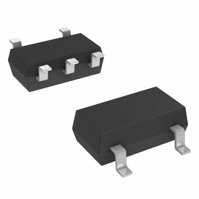
| 描述 | IC VOLT-DET 1.90V P-P SOT-23B监控电路 Push-Pull Low |
| 产品分类 | |
| 品牌 | Microchip Technology |
| 产品手册 | |
| 产品图片 |
|
| rohs | 符合RoHS无铅 / 符合限制有害物质指令(RoHS)规范要求 |
| 产品系列 | 电源管理 IC,监控电路,Microchip Technology MCP112T-195I/TT- |
| NumberofInputsMonitored | 1 Input |
| 数据手册 | http://www.microchip.com/mymicrochip/filehandler.aspx?ddocname=en020167http://www.microchip.com/mymicrochip/filehandler.aspx?ddocname=en023833 |
| 产品型号 | MCP112T-195I/TT |
| 产品种类 | 监控电路 |
| 人工复位 | No Manual Reset |
| 供应商器件封装 | SOT-23-3 |
| 包装 | 带卷 (TR) |
| 受监控电压数 | 1 |
| 商标 | Microchip Technology |
| 复位 | 低有效 |
| 复位超时 | - |
| 安装类型 | 表面贴装 |
| 安装风格 | SMD/SMT |
| 封装 | Reel |
| 封装/外壳 | TO-236-3,SC-59,SOT-23-3 |
| 封装/箱体 | SOT-23-3 |
| 工作温度 | -40°C ~ 85°C |
| 工作电源电流 | 1 uA |
| 工厂包装数量 | 3000 |
| 最大工作温度 | + 85 C |
| 最小工作温度 | - 40 C |
| 标准包装 | 3,000 |
| 欠电压阈值 | 1.872 V |
| 电压-阈值 | 1.9V |
| 电池备用开关 | No Backup |
| 电源电压-最大 | 5.5 V |
| 电源电压-最小 | 1 V |
| 监视器 | No Watchdog |
| 类型 | Voltage Supervisory |
| 被监测输入数 | 1 Input |
| 输出 | 推挽式,图腾柱 |
| 输出类型 | Active Low, Push-Pull |
| 过电压阈值 | 1.929 V |
| 阈值电压 | 1.9 V |


- 商务部:美国ITC正式对集成电路等产品启动337调查
- 曝三星4nm工艺存在良率问题 高通将骁龙8 Gen1或转产台积电
- 太阳诱电将投资9.5亿元在常州建新厂生产MLCC 预计2023年完工
- 英特尔发布欧洲新工厂建设计划 深化IDM 2.0 战略
- 台积电先进制程称霸业界 有大客户加持明年业绩稳了
- 达到5530亿美元!SIA预计今年全球半导体销售额将创下新高
- 英特尔拟将自动驾驶子公司Mobileye上市 估值或超500亿美元
- 三星加码芯片和SET,合并消费电子和移动部门,撤换高东真等 CEO
- 三星电子宣布重大人事变动 还合并消费电子和移动部门
- 海关总署:前11个月进口集成电路产品价值2.52万亿元 增长14.8%


PDF Datasheet 数据手册内容提取
MCP111/112 Micropower Voltage Detector Features Description • Ultra-low supply current: 1.75µA (max.) The MCP111/112 are voltage-detecting devices (cid:127) Precision monitoring options of: designed to keep a microcontroller in reset until the system voltage has reached, and stabilized, at the - 1.90V, 2.32V, 2.63V, 2.90V, 2.93V, 3.08V, appropriate level for reliable system operation. These 4.38V and 4.63V devices also operate as protection from brown-out (cid:127) Resets microcontroller in a power-loss event conditions when the system supply voltage drops (cid:127) Active-low V OUT pin: below a safe operating level. The MCP111 and - MCP111 active-low, open-drain MCP112 are available in eight different trip voltages. - MCP112 active-low, push-pull The MCP111 has an open-drain output with an active- (cid:127) Available in SOT23-3, TO-92 and SC70 packages low pin (V ). This device will assert V when the OUT OUT (cid:127) Temperature Range: voltage on the VDD pin is below the trip-point voltage. - Extended: –40°C to +125°C The MCP112 has a push-pull output and will assert an (except MCP1XX-195) active-low signal (V pin) when the voltage on the OUT - Industrial: –40°C to +85°C (MCP1XX-195 only) VDD pin is below the trip-point voltage. During operation, the output (V ) remains at a logic- OUT Applications high as long as V is greater than the specified DD threshold voltage. When V falls below the voltage (cid:127) Critical µC and µP Power-monitoring Applications DD trip point, V is driven low. OUT (cid:127) Computers (cid:127) Intelligent Instruments Package Types (cid:127) Portable Battery-Powered Equipment SOT23-3/SC-70 Block Diagram VDD VOUT 1 M C P 11 3 VDD 1 Comparator /1 1 + Output VOUT VSS 2 2 Driver – TO-92 Band Gap Reference V OUT VDD VSS V SS 2004 Microchip Technology Inc. DS21889B-page 1
MCP111/112 1.0 ELECTRICAL † Notice: Stresses above those listed under “Maximum Rat- ings” may cause permanent damage to the device. This is a CHARACTERISTICS stress rating only and functional operation of the device at those or any other conditions above those indicated in the Absolute Maximum Ratings† operational listings of this specification is not implied. Expo- sure to maximum rating conditions for extended periods may VDD . . . . . . . . . . . . . . . . . . . . . . . . . . . . . . . . . . . . . . . . . 7.0V affect device reliability. Input current (V ) . . . . . . . . . . . . . . . . . . . . . . . . . . . .10mA DD Output current (RST) . . . . . . . . . . . . . . . . . . . . . . . . . .10mA Rated Rise Time of V . . . . . . . . . . . . . . . . . . . . . . 100V/µs DD All inputs and outputs w.r.t. V . . . . . –0.6V to (V + 1.0V) SS DD Storage temperature. . . . . . . . . . . . . . . . . .–65°C to + 150°C Ambient temp. with power applied . . . . . . .–40°C to + 125°C Maximum Junction temp. with power applied. . . . . . . .150°C ESD protection on all pins. . . . . . . . . . . . . . . . . . . . . . . . . ≥ 2kV DC CHARACTERISTICS Electrical Specifications: Unless otherwise indicated, all limits are specified for V = 1V to 5.5V, R = 100kΩ (only MCP111), DD PU T = –40°C to +125°C. A Parameters Sym Min Typ Max Units Conditions Operating Voltage Range V 1.0 — 5.5 V DD Specified V Value to V low V 1.0 — V I = 10µA, V < 0.2V DD OUT DD RST RST Operating Current I — < 1 1.75 µA DD V Trip Point MCP1XX-195 V 1.872 1.900 1.929 V T = +25°C (Note1) DD TRIP A 1.853 1.900 1.948 V T = -40°C to +85°C (Note2) A MCP1XX-240 2.285 2.320 2.355 V T = +25°C (Note1) A 2.262 2.320 2.378 V Note2 MCP1XX-270 2.591 2.630 2.670 V T = +25°C (Note1) A 2.564 2.630 2.696 V Note2 MCP1XX-290 2.857 2.900 2.944 V T = +25°C (Note1) A 2.828 2.900 2.973 V Note2 MCP1XX-300 2.886 2.930 2.974 V T = +25°C (Note1) A 2.857 2.930 3.003 V Note2 MCP1XX-315 3.034 3.080 3.126 V T = +25°C (Note1) A 3.003 3.080 3.157 V Note2 MCP1XX-450 4.314 4.380 4.446 V T = +25°C (Note1) A 4.271 4.380 4.490 V Note2 MCP1XX-475 4.561 4.630 4.700 V T = +25°C (Note1) A 4.514 4.630 4.746 V Note2 V Trip Point Tempco T — ±100 — ppm/ DD TPCO °C Threshold Hysteresis MCP1XX-195 V 0.019 — 0.114 V T = +25°C HYS A (min. = 1%, max = 6%) MCP1XX-240 0.023 — 0.139 V MCP1XX-270 0.026 — 0.158 V MCP1XX-290 0.029 — 0.174 V MCP1XX-300 0.029 — 0.176 V MCP1XX-315 0.031 — 0.185 V MCP1XX-450 0.044 — 0.263 V MCP1XX-475 0.046 — 0.278 V Note 1: Trip point is ±1.5% from typical value. 2: Trip point is ±2.5% from typical value. DS21889B-page 2 2004 Microchip Technology Inc.
MCP111/112 DC CHARACTERISTICS (CONTINUED) Electrical Specifications: Unless otherwise indicated, all limits are specified for V = 1V to 5.5V, R = 100kΩ (only MCP111), DD PU T = –40°C to +125°C. A Parameters Sym Min Typ Max Units Conditions V Low-level Output Voltage V — — 0.4 V I = 500µA, V = V OUT OL OL DD TRIP(MIN) V High-level Output Voltage V V – 0.6 — — V I = 1mA, For only MCP112 OUT OH DD OH (push-pull output) Open-Drain Output Leakage Current I — 0.1 — µA OD (MCP111 only) Note 1: Trip point is ±1.5% from typical value. 2: Trip point is ±2.5% from typical value. V TRIP 1V VDD tRPU t RPD V OH 1V V V OL OUT t RT FIGURE 1-1: Timing Diagram. AC CHARACTERISTICS Electrical Specifications: Unless otherwise indicated, all limits are specified for V = 1V to 5.5V, R = 100kΩ DD PU (only MCP111), T = –40°C to +125°C. A Parameters Sym Min Typ Max Units Conditions VDD Detect to VOUT Inactive tRPU — 90 — µs Figure1-1 and CL = 50pF (Note1) VDD Detect to VOUT Active tRPD — 130 — µs VDD ramped from VTRIP(MAX) + 250mV down to V – TRIP(MIN) 250mV, per Figure1-1, C = 50pF (Note1) L VOUT Rise Time After VOUT Active tRT — 5 — µs For VOUT 10% to 90% of final value per Figure1-1, C = 50pF L (Note1) Note 1: These parameters are for design guidance only and are not 100% tested. 2004 Microchip Technology Inc. DS21889B-page 3
MCP111/112 TEMPERATURE CHARACTERISTICS Electrical Specifications: Unless otherwise noted, all limits are specified for V = 1V to 5.5V, R = 100kΩ DD PU (only MCP111), T = –40°C to +125°C. A Parameters Sym Min Typ Max Units Conditions Temperature Ranges Specified Temperature Range T –40 — +85 °C MCP1XX-195 A Specified Temperature Range T –40 — +125 °C Except MCP1XX-195 A Maximum Junction Temperature T — — +150 °C J Storage Temperature Range T –65 — +150 °C A Package Thermal Resistances Thermal Resistance, 3L-SOT23 θ — 336 — °C/W JA Thermal Resistance, 3L-SC-70 θ — 340 — °C/W JA Thermal Resistance, 3L-TO92 θ — 131.9 — °C/W JA DS21889B-page 4 2004 Microchip Technology Inc.
MCP111/112 2.0 TYPICAL PERFORMANCE CURVES Note: The graphs and tables provided following this note are a statistical summary based on a limited number of samples and are provided for informational purposes only. The performance characteristics listed herein are not tested or guaranteed. In some graphs or tables, the data presented may be outside the specified operating range (e.g., outside specified power supply range) and therefore outside the warranted range. Note: Unless otherwise indicated, all limits are specified for V = 1V to 5.5V, R = 100kΩ (only MCP111; DD PU see Figure 4-1), T = –40°C to +125°C. A 1.6 1.6 1.4 MCP111-195 5.5V 1.4 MCP111-195 5.0V 1.2 1.2 +125°C I (uA)DD00..681 224...180VVV I (uA)DD00..681 +85°C -40°C 0.4 1.7V 0.4 0.2 1.0V 0.2 +25°C 0 0 0 0 0 0 0 0 0 0 0 0 1.0 2.0 3.0 4.0 5.0 6.0 4 2 2 4 6 8 0 2 4 - - 1 1 1 Temperature (°C) VDD (V) FIGURE 2-1: I vs. Temperature FIGURE 2-4: I vs. V (MCP111-195). DD DD DD (MCP111-195). 1.2 1.6 MCP112-300 5.5V MCP112-300 1.4 1 5.0V 1.2 0.8 4.0V A) A) 1 I (uDD00..46 12..78VV I (uDD 00..68 +85°C +125°C 2.1V 0.4 -40°C 0.2 1.0V 0.2 +25°C 0 0 40 20 0 20 40 60 80 00 20 40 1.0 2.0 3.0 4.0 5.0 6.0 - - 1 1 1 Temperature (°C) VDD (V) FIGURE 2-2: I vs. Temperature FIGURE 2-5: I vs. V (MCP112-300). DD DD DD (MCP112-300). 1 1.6 0.9 MCP112-475 5.5V 1.4 MCP112-475 0.8 1.2 I (uA)DD0000....4567 5.0V 1.7V4.0V 2.8V 2.1V I (uA)DD00..681 +85°C +125°C 0.3 0.4 -40°C 0.2 0.1 1.0V 0.2 +25°C 0 0 0 0 0 0 0 0 0 0 0 0 1.0 2.0 3.0 4.0 5.0 6.0 4 2 2 4 6 8 0 2 4 - - 1 1 1 V (V) Temperature (°C) DD FIGURE 2-3: IDD vs. Temperature FIGURE 2-6: IDD vs. VDD (MCP112-475). (MCP112-475). 2004 Microchip Technology Inc. DS21889B-page 5
MCP111/112 Note: Unless otherwise indicated, all limits are specified for V = 1V to 5.5V, R = 100kΩ (only MCP111; DD PU see Figure 4-1), T = –40°C to +125°C. A 0.120 1.950 0.050 MCP111-195 1.945 VTRIP, V increasing 0.045 0.100 VDD = 1.7V 11..993450 VHYS, Hysteresis 00..003450 0.080 +125°C V (V)TRIP1111....999912235050 Mm+8Ca5xP° C1te1m1-p1 9is5 000...000223050 Hyst (V) V (V)OL00..004600 +85°C 1.910 0.015 -40°C 1.905 VTRIP, V decreasing 0.010 0.020 +25°C 1.900 0.005 1.895 0.000 0.000 -60 -10 40 90 140 0.00 0.25 0.50 0.75 1.00 Temperature (°C) I (mA) OL FIGURE 2-7: V and V vs. FIGURE 2-10: V vs. I TRIP HYST OL OL Temperature (MCP111-195). (MCP111-195 @V = 1.7V). DD 0.080 3.040 0.100 MCP112-300 3.020 VTRIP, V increasing 0.098 00..006700 VDD = 2.7V 0.096 V (V)TRIP 223...990680000 MCP1V1H2Y-S3, 0H0ysteresis 0000....000089998024 Hyst (V) V (V)OL 000...000345000 +85°C +125°C 2.940 0.020 -40°C 0.086 2.920 VTRIP, V decreasing 0.084 0.010 +25°C 2.900 0.082 0.000 -60 -10 40 90 140 0.00 0.25 0.50 0.75 1.00 Temperature (°C) IOL (mA) FIGURE 2-8: V and V vs. FIGURE 2-11: V vs. I TRIP HYST OL OL Temperature (MCP112-300). (MCP112-300 @V = 2.7V). DD 4.800 0.180 0.050 MCP112-475 44..776800 VTRIP, V increasing 0.170 0.040 VDD = 4.4V 4.740 0.160 V (V)TRIP 4444....667768020000 MVCHPYS1,1 H2-y4s7t5eresis 000...111345000 Hyst (V) V (V)OL 00..002300 +85°C +125°C 4.640 0.120 -40°C 4.620 0.010 0.110 +25°C 4.600 VTRIP, V decreasing 4.580 0.100 0.000 -60 -20 20 60 100 140 0.00 0.25 0.50 0.75 1.00 Temperature (°C) IOL (mA) FIGURE 2-9: V and V vs. FIGURE 2-12: V vs. I TRIP HYST OL OL Temperature (MCP112-475). (MCP112-475 @V = 4.4V). DD DS21889B-page 6 2004 Microchip Technology Inc.
MCP111/112 Note: Unless otherwise indicated, all limits are specified for V = 1V to 5.5V, R = 100kΩ (only MCP111; DD PU see Figure 4-1), T = –40°C to +125°C. A 0.120 3.150 MCP111-195 IOL = 1.00 mA MCP112-300 0.100 VDD = 1.7 V VDD = 3.1V 3.100 0.080 IOL = 0.75 mA V (V)OL 0.060 IOL = 0.50 mA V (V)OH 33..000500 -40 °C +25 °C 0.040 IOL = 0.25 mA 0.020 2.950 +85 °C IOL = 0.00 mA +125 °C 0.000 2.900 -40 0 40 80 120 0.00 0.25 0.50 0.75 1.00 Temperature (°C) IOL (mA) FIGURE 2-13: V vs. Temperature FIGURE 2-16: V vs. I OL OH OH (MCP111-195 @ V = 1.7V). (MCP112-300 @ V = 3.1V). DD DD 0.080 4.820 0.070 MVDCDP =1 122.7-V300 IOL = 1.00 mA 4.800 MVDCDP =1 41.28-V475 0.060 0.050 IOL = 0.75 mA 4.780 +25 °C V (V)OL00..003400 IOL = 0.50 mA V (V)OH 44..774600 -40 °C 0.020 IOL = 0.25 mA 4.720 +85 °C 0.010 4.700 IOL = 0.00 mA +125 °C 0.000 4.680 -40 0 40 80 120 0.00 0.25 0.50 0.75 1.00 Temperature (°C) I (mA) OL FIGURE 2-14: V vs. Temperature FIGURE 2-17: V vs. I OL OH OH (MCP112-300 @ V = 2.7V). (MCP112-475 @ V = 4.8V). DD DD 0.050 600 MCP112-475 IOL = 1.00 mA 0.040 VDD = 4.4V µs) 500 MCP111-195 IOL = 0.75 mA n ( V (V)OL 00..002300 IIOOLL == 00..2550 mmAA sient Duratio 234000000 MMCCPP111122--437050 0.010 Tran 100 IOL = 0.00 mA 0.000 0 -40 0 40 80 120 0.001 0.01 0.1 1 10 Temperature (°C) V (min) - V TRIP DD FIGURE 2-15: V vs. Temperature FIGURE 2-18: Typical Transient Response OL (MCP112-475 @ V = 4.4V). (25 °C). DD 2004 Microchip Technology Inc. DS21889B-page 7
MCP111/112 Note: Unless otherwise indicated, all limits are specified for V = 1V to 5.5V, R = 100kΩ (only MCP111; DD PU see Figure 4-1), T = –40°C to +125°C. A 350 400 MCP111-195 MCP111-195 300 V5VDD - d1e.7cVreasing from: 350 300 µs) 220500 VVDTRDI Pd(meacxr) e+a 0s.i2n5gV f rtoom V:TRIP(min) - 0.25V µs) 250 V0VDD - i2n.c1rVeasing from: t (RPD 150 t (RPU 125000 VDD increasing from: 100 100 0V - 2.8V VDD increasing VDD decreasing from: from: 0V - 4.0V 50 5V - 0V 50 VDD increasing from: 0V - 5.5V 0 0 -40 -15 10 35 60 85 110 -40 -15 10 35 60 85 110 Temperature (°C) Temperature (°C) FIGURE 2-19: t vs. Temperature FIGURE 2-22: t vs. Temperature RPD RPU (MCP111-195). (MCP111-195). 160 140 140 MCP112-300 VVDTRDI Pd(meacxr) e+a 0s.i2n5gV f rtoom V:TRIP(min) - 0.25V 120 V0VDD - i3n.c1rVeasing from: MCP112-300 120 100 µs) 100 VDD decreasing from: µs) 80 V0VDD - i3n.c3rVeasing from: t (RPD 6800 5V - 2.7V t (RPU 60 V0VDD - i4n.c0rVeasing from: 40 40 20 V5VDD - d0eVcreasing from: 20 VDD increasing from: 0V - 5.5V 0 0 -40 -15 10 35 60 85 110 -40 -15 10 35 60 85 110 Temperature (°C) Temperature (°C) FIGURE 2-20: t vs. Temperature FIGURE 2-23: t vs. Temperature RPD RPU (MCP112-300). (MCP112-300). 250 250 MCP112-475 MCP112-475 200 V5VDD - d4e.4cVreasing from: 200 VDD increasing from: 0V - 4.9V s) 150 s) 150 µ µ t (RPD 100 VVDTRDI Pd(meacxr) e+a 0s.in25gV f rtoom V:TRIP(min) - 0.25V t (RPU 100 V0VDD - i5n.c0rVeasing from: VDD increasing from: 50 50 0V - 5.5V VDD decreasing from: 5V - 0V 0 0 -40 -15 10 35 60 85 110 -40 -15 10 35 60 85 110 Temperature (°C) Temperature (°C) FIGURE 2-21: t vs. Temperature FIGURE 2-24: t vs. Temperature RPD RPU (MCP112-475). (MCP112-475). DS21889B-page 8 2004 Microchip Technology Inc.
MCP111/112 Note: Unless otherwise indicated, all limits are specified for V = 1V to 5.5V, R = 100kΩ (only MCP111; DD PU see Figure 4-1), T = –40°C to +125°C. A 60 0.1500 MCP111-195 MCP112-475 55 0.1400 50 VDD increasing from: 0.1300 VDD increasing from: t (µs)RT 344505 0V - 2.1V V0VDD - i5n.c5rVeasing from: VfrDoDm in: c0rVe a- s4i.n0gV t (µs)RT 00..11120000 V0VDD - i4n.c9rVeasing from: 0V - 5.0V 30 0.1000 VDD increasing from: 0V - 5.5V 25 VDD increasing from: 0.0900 VDD increasing from: 0V - 2.8V 0V - 4.8V 20 0.0800 -40 -15 10 35 60 85 110 -40 -15 10 35 60 85 110 Temperature (°C) Temperature (°C) FIGURE 2-25: t vs. Temperature FIGURE 2-27: t vs. Temperature RT RT (MCP111-195). (MCP112-475). 0.4 VDD increasing from: 0.35 0V - 3.1V VDD increasing from: 0.3 0V - 3.3V 0.25 s) t (µRT 0.01.52 V0VDD - i5n.c5rVeasing from: 0.1 VDD increasing from: 0V - 4.0V 0.05 MCP112-300 0 -40 -15 10 35 60 85 110 Temperature (°C) FIGURE 2-26: t vs. Temperature RT (MCP112-300). 2004 Microchip Technology Inc. DS21889B-page 9
MCP111/112 3.0 PIN DESCRIPTION The descriptions of the pins are listed in Table3-1. TABLE 3-1: PIN FUNCTION TABLE Pin No. Symbol Function SOT23-3 T0-92 SC-70 1 1 V Output State OUT V Falling: DD H = V > V DD TRIP L = V < V DD TRIP V Rising: DD H = V > V + V DD TRIP HYS L = V < V + V DD TRIP HYS 2 3 V Ground reference SS 3 2 V Positive power supply DD DS21889B-page 10 2004 Microchip Technology Inc.
MCP111/112 4.0 APPLICATION INFORMATION 4.1 V Operation TRIP For many of today’s microcontroller applications, care The voltage trip point (V ) is determined on the falling TRIP must be taken to prevent low-power conditions that can edge of V . The actual voltage trip point (V ) will DD TRIPAC cause many different system problems. The most be between the minimum trip point (V ) and the TRIPMIN common causes are brown-out conditions, where the maximum trip point (V ). There is a hysteresis on TRIPMAX system supply drops below the operating level momen- this trip point to remove any “jitter” that would occur on tarily. The second most common cause is when a slowly the V pin when the device V is at the trip point. OUT DD decaying power supply causes the microcontroller to Figure4-2 shows the state of the V pin as deter- OUT begin executing instructions without sufficient voltage to mined by the V voltage. The V specification is for DD TRIP sustain SRAM, thus producing indeterminate results. falling V voltages. When the V voltage is rising, the DD DD Figure4-1 shows a typical application circuit. V pin will not be driven high until V is at V + OUT DD TRIP V . HYS V DD 3 V DD V 0.1 DD R PICmicro® MCP11X PU Microcontroller µF 1 VOUT MCLR (Reset Input) V SS GND 2 Note1: R may be required with the MCP111 PU due to the open-drain output. Resistor R is not required with the MCP112. PU FIGURE 4-1: Typical Application Circuit. V DD V + V V TRIPAC HYSAC TRIPMAX V TRIPAC VTRIPMIN VTRIPAC 1V V OUT < 1 V is outside the device specifications FIGURE 4-2: V Operation as Determined by the V and V . OUT TRIP HYS 2004 Microchip Technology Inc. DS21889B-page 11
MCP111/112 4.2 Negative Going V Transients 4.3 Effect of Temperature on Time-out DD Period (t ) The minimum pulse width (time) required to cause a RPU reset may be an important criteria in the implementa- The time-out period (t ) determines how long the RPU tion of a POR circuit. This time is referred to as device remains in the reset condition. This is affected transient duration and is the amount of time needed for by both V and temperature. The graph shown in DD these supervisory devices to respond to a drop in VDD. Figures2-22, 2-23 and 2-24 show the typical The transient duration time is dependant on the magni- response for different V values and temperatures. DD tude of V – V . Generally speaking, the transient TRIP DD duration decreases with increases in V – V . TRIP DD Figure4-3 shows a typical transient duration vs. reset comparator overdrive for which the MCP111/112 will not generate a reset pulse. It shows that the farther below the trip point the transient pulse goes, the duration of the pulse required to cause a reset gets shorter. Figure2-18 shows the transient response characteristics for the MCP111/112. A 0.1µF bypass cap mounted as close as possible to the V pin provides additional transient immunity DD (refer to Figure4-1). 5V V TRIP(MAX) e V g TRIP(MIN) a olt VTRIP(MIN) - VDD V y pl p u tTRANS S 0V Time (µs) FIGURE 4-3: Example of Typical Transient Duration Waveform. DS21889B-page 12 2004 Microchip Technology Inc.
MCP111/112 5.0 PACKAGING INFORMATION 5.1 Package Marking Information 3-Lead TO-92 Example: XXXXXX MCP111 XXXXXX 290E XXXXXX TO0405 YWWNNN 256 3-Pin SC-70 Example: Part Number SC-70 Part Number SC-70 MCP111T-195I/LB EPN MCP112T-195I/LB ERN (cid:99) (cid:100) (cid:101) MCP111T-240E/LB EQN MCP112T-240E/LB ESN MCP111T-270E/LB EGN MCP112T-270E/LB EAN MCP111T-290E/LB EHN MCP112T-290E/LB EBN MCP111T-300E/LB EJN MCP112T-300E/LB ECN Top Side MCP111T-315E/LB EKN MCP112T-315E/LB EDN MCP111T-450E/LB ELN MCP112T-450E/LB EEN MCP111T-475E/LB EMN MCP112T-475E/LB EFN 3-Pin SOT-23B Example: Part Number SOT-23 Part Number SOT-23 MCP111T-195I/TT MPNN MCP112T-195I/TT MRNN (cid:99)(cid:100)(cid:101)(cid:102) MCP111T-240ETT MQNN MCP112T-240ETT MSNN MCP111T-270E/TT MGNN MCP112T-270E/TT MANN MCP111T-290E/TT NHNN MCP112T-290E/TT MBNN MCP111T-300E/TT MJNN MCP112T-300E/TT MCNN MCP111T-315E/TT MKNN MCP112T-315E/TT MDNN MCP111T-450E/TT MLNN MCP112T-450E/TT MENN MCP111T-475E/TT MMNN MCP112T-475E/TT MFNN Legend: 1 Part Number + temperature range and voltage (two-digit code) 2 Part Number + temperature range and voltage (two-digit code) 3 Lot ID number 4 Year and work week Note: In the event the full Microchip part number cannot be marked on one line, it will be carried over to the next line thus limiting the number of available characters for customer specific information. 2004 Microchip Technology Inc. DS21889B-page 13
MCP111/112 3-Lead Plastic Small Outline Transistor (TT) (SOT-23) E E1 2 B p1 D n p 1 α c A A2 φ A1 β L Units INCHES* MILLIMETERS Dimension Limits MIN NOM MAX MIN NOM MAX Number of Pins n 3 3 Pitch p .038 0.96 Outside lead pitch (basic) p1 .076 1.92 Overall Height A .035 .040 .044 0.89 1.01 1.12 Molded Package Thickness A2 .035 .037 .040 0.88 0.95 1.02 Standoff § A1 .000 .002 .004 0.01 0.06 0.10 Overall Width E .083 .093 .104 2.10 2.37 2.64 Molded Package Width E1 .047 .051 .055 1.20 1.30 1.40 Overall Length D .110 .115 .120 2.80 2.92 3.04 Foot Length L .014 .018 .022 0.35 0.45 0.55 Foot Angle φ 0 5 10 0 5 10 Lead Thickness c .004 .006 .007 0.09 0.14 0.18 Lead Width B .015 .017 .020 0.37 0.44 0.51 Mold Draft Angle Top α 0 5 10 0 5 10 Mold Draft Angle Bottom β 0 5 10 0 5 10 * Controlling Parameter § Significant Characteristic Notes: Dimensions D and E1 do not include mold flash or protrusions. Mold flash or protrusions shall not exceed .010” (0.254mm) per side. JEDEC Equivalent: TO-236 Drawing No. C04-104 DS21889B-page 14 2004 Microchip Technology Inc.
MCP111/112 3-Lead Plastic Small Outline Transistor (LB) (SC-70) E E1 B 2 p1 D 3 p 1 a c A A2 b L A1 Units INCHES MILLIMETERS* Dimension Limits MIN MAX MIN MAX Number of Pins 3 3 Pitch p .026 BSC. 0.65 BSC. Outside lead pitch (basic) p1 .051 BSC. 1.30 BSC. Overall Height A .031 .043 0.80 1.10 Molded Package Thickness A2 .031 .039 0.80 1.00 Standoff A1 .000 .0004 0.00 .010 Overall Width E .071 .094 1.80 2.40 Molded Package Width E1 .045 .053 1.15 1.35 Overall Length D .071 .089 1.80 2.25 Foot Length L .004 .016 0.10 0.41 Lead Thickness c .003 .010 0.08 0.25 Lead Width B .006 .016 0.15 0.40 Mold Draft Angle Top a 8° 12° 8° 12° Mold Draft Angle Bottom b 8° 12° 8° 12° *Controlling Parameter Notes: Dimensions D and E1 do not include mold flash or protrusions. Mold flash or protrusions shall not exceed .005" (0.127mm) per side. JEITA (EIAJ) Equivalent: SC70 Drawing No. C04-104 2004 Microchip Technology Inc. DS21889B-page 15
MCP111/112 3-Lead Plastic Transistor Outline (TO) (TO-92) E1 D 1 n L 1 2 3 α B p c A R β Units INCHES* MILLIMETERS Dimension Limits MIN NOM MAX MIN NOM MAX Number of Pins n 3 3 Pitch p .050 1.27 Bottom to Package Flat A .130 .143 .155 3.30 3.62 3.94 Overall Width E1 .175 .186 .195 4.45 4.71 4.95 Overall Length D .170 .183 .195 4.32 4.64 4.95 Molded Package Radius R .085 .090 .095 2.16 2.29 2.41 Tip to Seating Plane L .500 .555 .610 12.70 14.10 15.49 Lead Thickness c .014 .017 .020 0.36 0.43 0.51 Lead Width B .016 .019 .022 0.41 0.48 0.56 Mold Draft Angle Top α 4 5 6 4 5 6 Mold Draft Angle Bottom β 2 3 4 2 3 4 *Controlling Parameter Notes: Dimensions D and E1 do not include mold flash or protrusions. Mold flash or protrusions shall not exceed .010” (0.254mm) per side. JEDEC Equivalent: TO-92 Drawing No. C04-101 DS21889B-page 16 2004 Microchip Technology Inc.
MCP111/112 5.2 Product Tape and Reel Specifications FIGURE 5-1: EMBOSSED CARRIER DIMENSIONS (8, 12, 16 AND 24 MM TAPE ONLY) Top Cover Tape A 0 W K0 B0 P TABLE 1: CARRIER TAPE/CAVITY DIMENSIONS Carrier Cavity Dimensions Dimensions Output Reel Case Package Quantity Diameter in Outline Type W P A0 B0 K0 Units mm mm mm mm mm mm TT SOT-23B 3L 8 4 3.15 2.77 1.22 3000 180 LB SC-70 3L 8 4 2.4 2.4 1.19 3000 180 FIGURE 5-2: 3-LEAD SOT-23/SC70 DEVICE TAPE AND REEL SPECIFICATIONS gnikraM Device User Direction of Feed eciveD Marking W, Width Pin 1 of Carrier Tape Pin 1 P, Pitch Standard Reel Component Orientation Reverse Reel Component Orientation 2004 Microchip Technology Inc. DS21889B-page 17
MCP111/112 FIGURE 5-3: TO-92 DEVICES P, Pitch Device Marking 3 LEAD TO-92 W, Width of Carrier Tape Device Marking 2 LEAD TO-92 W, Width of Carrier Tape Standard Reel Reverse Reel Component Orientation Component Orientation H 1 H W6 H 0 D F1 F F2 P1 P 2 DS21889B-page 18 2004 Microchip Technology Inc.
MCP111/112 PRODUCT IDENTIFICATION SYSTEM To order or obtain information, e.g., on pricing or delivery, refer to the factory or the listed sales office. PART NO. X XXX X XX Examples: a) MCP111T-195I/TT: Tape and Reel, Device Tape/Reel Monitoring Temperature Package 1.95V option, open-drain, Option Options Range -40°C to +85°C, SOT-23B package. b) MCP111T-315E/LB:Tape and Reel, 3.15V option, open-drain, Device: MCP111: MicroPower Voltage Detector, open-drain -40°C to +125°C, MCP111T:MicroPower Voltage Detector, open-drain SC-70-3 package. (Tape and Reel) c) MCP111-300E/TO: 3.00V option, open-drain, MCP112: MicroPower Voltage Detector, push-pull -40°C to +125°C, MCP112T:MicroPower Voltage Detector, push-pull TO-92-3 package. (Tape and Reel) a) MCP112T-290E/TT:Tape and Reel, 2.90V option, push-pull, - Monitoring Options: 195 = 1.90V 40°C to +125°C, 240 = 2.32V SOT-23B-3 package. 270 = 2.63V b) MCP112T-475E/LB:Tape and Reel, 290 = 2.90V 4.75V option, push-pull, 300 = 2.93V -40°C to +125°C, 315 = 3.08V SC-70-3 package. 450 = 4.38V c) MCP112-450E/TO: 4.5V option, push-pull, 475 = 4.63V -40°C to +125°C, TO-92-3 package. Temperature Range: I = -40°C to +85°C (MCP11X-195 only) E = -40°C to +125°C (Except MCP11X-195 only) Package: TT = SOT-23B, 3-lead LB = SC-70, 3-lead TO = TO-92, 3-lead Sales and Support Data Sheets Products supported by a preliminary Data Sheet may have an errata sheet describing minor operational differences and recommended workarounds. To determine if an errata sheet exists for a particular device, please contact one of the following: 1. Your local Microchip sales office 2. The Microchip Corporate Literature Center U.S. FAX: (480) 792-7277 3. The Microchip Worldwide Site (www.microchip.com) Please specify which device, revision of silicon and Data Sheet (include Literature #) you are using. Customer Notification System Register on our web site (www.microchip.com/cn) to receive the most current information on our products. 2004 Microchip Technology Inc. DS21889B-page 19
MCP111/112 NOTES: DS21889B-page 20 2004 Microchip Technology Inc.
Note the following details of the code protection feature on Microchip devices: (cid:127) Microchip products meet the specification contained in their particular Microchip Data Sheet. (cid:127) Microchip believes that its family of products is one of the most secure families of its kind on the market today, when used in the intended manner and under normal conditions. (cid:127) There are dishonest and possibly illegal methods used to breach the code protection feature. All of these methods, to our knowledge, require using the Microchip products in a manner outside the operating specifications contained in Microchip’s Data Sheets. Most likely, the person doing so is engaged in theft of intellectual property. (cid:127) Microchip is willing to work with the customer who is concerned about the integrity of their code. (cid:127) Neither Microchip nor any other semiconductor manufacturer can guarantee the security of their code. Code protection does not mean that we are guaranteeing the product as “unbreakable.” Code protection is constantly evolving. We at Microchip are committed to continuously improving the code protection features of our products. Attempts to break Microchip’s code protection feature may be a violation of the Digital Millennium Copyright Act. If such acts allow unauthorized access to your software or other copyrighted work, you may have a right to sue for relief under that Act. Information contained in this publication regarding device Trademarks applications and the like is intended through suggestion only The Microchip name and logo, the Microchip logo, Accuron, and may be superseded by updates. It is your responsibility to dsPIC, KEELOQ, microID, MPLAB, PIC, PICmicro, ensure that your application meets with your specifications. PICSTART, PROMATE, PowerSmart, rfPIC, and No representation or warranty is given and no liability is SmartShunt are registered trademarks of Microchip assumed by Microchip Technology Incorporated with respect Technology Incorporated in the U.S.A. and other countries. to the accuracy or use of such information, or infringement of patents or other intellectual property rights arising from such AmpLab, FilterLab, MXDEV, MXLAB, PICMASTER, SEEVAL, use or otherwise. Use of Microchip’s products as critical SmartSensor and The Embedded Control Solutions Company components in life support systems is not authorized except are registered trademarks of Microchip Technology with express written approval by Microchip. No licenses are Incorporated in the U.S.A. conveyed, implicitly or otherwise, under any intellectual Analog-for-the-Digital Age, Application Maestro, dsPICDEM, property rights. dsPICDEM.net, dsPICworks, ECAN, ECONOMONITOR, FanSense, FlexROM, fuzzyLAB, In-Circuit Serial Programming, ICSP, ICEPIC, Migratable Memory, MPASM, MPLIB, MPLINK, MPSIM, PICkit, PICDEM, PICDEM.net, PICLAB, PICtail, PowerCal, PowerInfo, PowerMate, PowerTool, rfLAB, rfPICDEM, Select Mode, Smart Serial, SmartTel and Total Endurance are trademarks of Microchip Technology Incorporated in the U.S.A. and other countries. SQTP is a service mark of Microchip Technology Incorporated in the U.S.A. All other trademarks mentioned herein are property of their respective companies. © 2004, Microchip Technology Incorporated, Printed in the U.S.A., All Rights Reserved. Printed on recycled paper. Microchip received ISO/TS-16949:2002 quality system certification for its worldwide headquarters, design and wafer fabrication facilities in Chandler and Tempe, Arizona and Mountain View, California in October 2003. The Company’s quality system processes and procedures are for its PICmicro® 8-bit MCUs, KEELOQ® code hopping devices, Serial EEPROMs, microperipherals, nonvolatile memory and analog products. In addition, Microchip’s quality system for the design and manufacture of development systems is ISO 9001:2000 certified. 2004 Microchip Technology Inc. DS21889B-page 21
WORLDWIDE SALES AND SERVICE AMERICAS ASIA/PACIFIC ASIA/PACIFIC EUROPE Corporate Office Australia - Sydney India - Bangalore Austria - Weis 2355 West Chandler Blvd. Tel: 61-2-9868-6733 Tel: 91-80-2229-0061 Tel: 43-7242-2244-399 Chandler, AZ 85224-6199 Fax: 61-2-9868-6755 Fax: 91-80-2229-0062 Fax: 43-7242-2244-393 Tel: 480-792-7200 China - Beijing India - New Delhi Denmark - Ballerup Fax: 480-792-7277 Tel: 86-10-8528-2100 Tel: 91-11-5160-8632 Tel: 45-4420-9895 Technical Support: Fax: 86-10-8528-2104 Fax: 91-11-5160-8632 Fax: 45-4420-9910 480-792-7627 Web Address: China - Chengdu Japan - Kanagawa France - Massy www.microchip.com Tel: 86-28-8676-6200 Tel: 81-45-471- 6166 Tel: 33-1-69-53-63-20 Fax: 86-28-8676-6599 Fax: 81-45-471-6122 Fax: 33-1-69-30-90-79 Atlanta Alpharetta, GA China - Fuzhou Korea - Seoul Germany - Ismaning Tel: 770-640-0034 Tel: 86-591-750-3506 Tel: 82-2-554-7200 Tel: 49-89-627-144-0 Fax: 770-640-0307 Fax: 86-591-750-3521 Fax: 82-2-558-5932 or Fax: 49-89-627-144-44 China - Hong Kong SAR 82-2-558-5934 Italy - Milan Boston Westford, MA Tel: 852-2401-1200 Singapore Tel: 39-0331-742611 Tel: 978-692-3848 Fax: 852-2401-3431 Tel: 65-6334-8870 Fax: 39-0331-466781 Fax: 978-692-3821 China - Shanghai Fax: 65-6334-8850 Netherlands - Drunen Chicago Tel: 86-21-6275-5700 Taiwan - Kaohsiung Tel: 31-416-690399 Itasca, IL Fax: 86-21-6275-5060 Tel: 886-7-536-4816 Fax: 31-416-690340 Tel: 630-285-0071 China - Shenzhen Fax: 886-7-536-4817 England - Berkshire Fax: 630-285-0075 Tel: 86-755-8290-1380 Taiwan - Taipei Tel: 44-118-921-5869 Dallas Fax: 86-755-8295-1393 Tel: 886-2-2500-6610 Fax: 44-118-921-5820 Addison, TX China - Shunde Fax: 886-2-2508-0102 Tel: 972-818-7423 Tel: 86-757-2839-5507 Taiwan - Hsinchu Fax: 972-818-2924 Fax: 86-757-2839-5571 Tel: 886-3-572-9526 Detroit China - Qingdao Fax: 886-3-572-6459 Farmington Hills, MI Tel: 86-532-502-7355 Tel: 248-538-2250 Fax: 86-532-502-7205 Fax: 248-538-2260 Kokomo Kokomo, IN Tel: 765-864-8360 Fax: 765-864-8387 Los Angeles Mission Viejo, CA Tel: 949-462-9523 Fax: 949-462-9608 San Jose Mountain View, CA Tel: 650-215-1444 Fax: 650-961-0286 Toronto Mississauga, Ontario, Canada Tel: 905-673-0699 Fax: 905-673-6509 08/24/04 DS21889B-page 22 2004 Microchip Technology Inc.
Mouser Electronics Authorized Distributor Click to View Pricing, Inventory, Delivery & Lifecycle Information: M icrochip: MCP111T-240E/LB MCP111T-240E/TT MCP112T-450E/TT MCP112T-450E/LB MCP111-315E/TO MCP112- 290E/TO MCP112T-290E/TT MCP112T-290E/LB MCP112-270E/TO MCP111T-450E/LB MCP111T-450E/TT MCP111T-270E/LB MCP111T-270E/TT MCP112-450E/TO MCP112T-240E/TT MCP112T-240E/LB MCP112T- 475E/LB MCP112T-475E/TT MCP112-240E/TO MCP112-475E/TO MCP112T-315E/TT MCP112T-315E/LB MCP112T-300E/TT MCP112T-300E/LB MCP112-195I/TO MCP111T-300E/TT MCP111T-300E/LB MCP111T- 195I/LB MCP111T-195I/TT MCP111-300E/TO MCP111-270E/TO MCP111-240E/TO MCP112T-270E/TT MCP112T- 270E/LB MCP112-315E/TO MCP111-450E/TO MCP111-290E/TO MCP112-300E/TO MCP111T-290E/LB MCP111T-290E/TT MCP111T-475E/TT MCP111T-475E/LB MCP111T-315E/TT MCP111T-315E/LB MCP112T- 195I/LB MCP112T-195I/TT