ICGOO在线商城 > 分立半导体产品 > 二极管 - 整流器 - 单 > MCL103A-TR3
 Datasheet下载
- 型号: MCL103A-TR3
- 制造商: Vishay
- 库位|库存: xxxx|xxxx
- 要求:
| 数量阶梯 | 香港交货 | 国内含税 |
| +xxxx | $xxxx | ¥xxxx |
查看当月历史价格
查看今年历史价格
MCL103A-TR3产品简介:
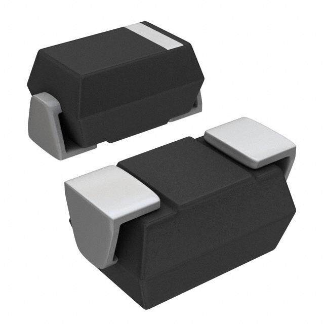
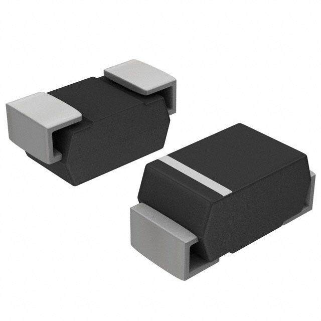
ICGOO电子元器件商城为您提供MCL103A-TR3由Vishay设计生产,在icgoo商城现货销售,并且可以通过原厂、代理商等渠道进行代购。 MCL103A-TR3价格参考。VishayMCL103A-TR3封装/规格:二极管 - 整流器 - 单, 肖特基 表面贴装 二极管 40V 200mA MicroMELF。您可以下载MCL103A-TR3参考资料、Datasheet数据手册功能说明书,资料中有MCL103A-TR3 详细功能的应用电路图电压和使用方法及教程。
Vishay Semiconductor Diodes Division生产的MCL103A-TR3是一款单整流二极管,广泛应用于各种电力电子设备中。该型号的二极管具有低正向压降、高浪涌电流能力以及快速恢复时间等特点,适用于多种应用场景。

 1. 电源适配器与充电器
MCL103A-TR3常用于开关电源(SMPS)和线性电源中的整流电路。在这些应用中,它能够将交流电转换为直流电,确保输出电压稳定可靠。其低正向压降有助于提高电源效率,减少热量产生,延长设备寿命。

 2. 电机驱动与逆变器
在电机驱动和逆变器系统中,MCL103A-TR3可以作为续流二极管或箝位二极管使用。当电机停止或减速时,二极管能够吸收反电动势,保护电路中的其他元件免受损坏。此外,在逆变器中,它可以用于直流到交流的转换过程中,确保电流的单向流动。

 3. 不间断电源(UPS)
在不间断电源系统中,MCL103A-TR3用于电池充电和放电管理。它可以在市电正常时将交流电整流为直流电给电池充电,并在市电中断时将电池的直流电转换为稳定的交流电输出,保证负载设备的持续运行。

 4. 太阳能光伏系统
在太阳能光伏系统中,MCL103A-TR3可用于最大功率点跟踪(MPPT)控制器和逆变器中。它能够有效地将太阳能板产生的直流电转换为可用的交流电,并且其快速恢复特性有助于提高系统的整体效率。

 5. 工业自动化设备
在工业自动化领域,如PLC、传感器和执行器等设备中,MCL103A-TR3可以用于信号隔离、保护电路和电源整流。其高浪涌电流能力使其能够在瞬态电压波动较大的环境中保持稳定工作。

总之,MCL103A-TR3凭借其优异的电气性能和可靠性,适用于多种电力电子应用,特别是在需要高效整流和保护的关键场合中表现出色。
| 参数 | 数值 |
| 产品目录 | |
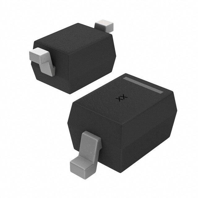
| 描述 | DIODE SCHOTTKY 40V MICROMELF肖特基二极管与整流器 400mA 40 Volt 15 Amp IFSM |
| 产品分类 | 单二极管/整流器分离式半导体 |
| 品牌 | Vishay Semiconductor Diodes DivisionVishay Semiconductors |
| 产品手册 | |
| 产品图片 | |
| rohs | 符合RoHS无铅 / 符合限制有害物质指令(RoHS)规范要求 |
| 产品系列 | 二极管与整流器,肖特基二极管与整流器,Vishay Semiconductors MCL103A-TR3- |
| 数据手册 | |
| 产品型号 | MCL103A-TR3MCL103A-TR3 |
| 不同If时的电压-正向(Vf) | 600mV @ 200mA |
| 不同 Vr、F时的电容 | 50pF @ 0V,1MHz |
| 不同 Vr时的电流-反向漏电流 | 5µA @ 10V |
| 二极管类型 | |
| 产品 | Schottky Diodes |
| 产品种类 | 肖特基二极管与整流器 |
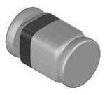
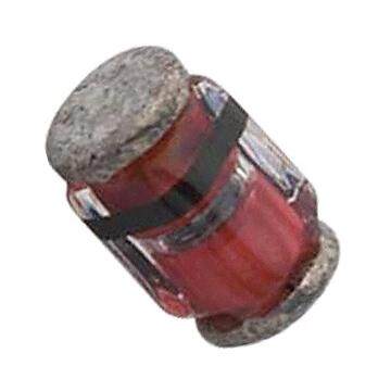
| 供应商器件封装 | MicroMELF |
| 包装 | 带卷 (TR) |
| 反向恢复时间(trr) | 10ns |
| 商标 | Vishay Semiconductors |
| 安装类型 | 表面贴装 |
| 安装风格 | SMD/SMT |
| 封装 | Reel |
| 封装/外壳 | 2-SMD |
| 封装/箱体 | Micro MELF |
| 峰值反向电压 | 40 V |
| 工作温度-结 | 125°C (最大) |
| 工作温度范围 | + 125 C |
| 工厂包装数量 | 10000 |
| 恢复时间 | 10 ns |
| 技术 | Silicon |
| 最大反向漏泄电流 | 5 uA |
| 最大工作温度 | + 125 C |
| 最大浪涌电流 | 15 A |
| 最小工作温度 | - 65 C |
| 标准包装 | 10,000 |
| 正向电压下降 | 0.6 V |
| 正向连续电流 | 0.2 A |
| 电压-DC反向(Vr)(最大值) | 40V |
| 电流-平均整流(Io) | 200mA |
| 速度 | 小信号 =< 200mA(Io),任意速度 |
| 配置 | Single |


- 商务部:美国ITC正式对集成电路等产品启动337调查
- 曝三星4nm工艺存在良率问题 高通将骁龙8 Gen1或转产台积电
- 太阳诱电将投资9.5亿元在常州建新厂生产MLCC 预计2023年完工
- 英特尔发布欧洲新工厂建设计划 深化IDM 2.0 战略
- 台积电先进制程称霸业界 有大客户加持明年业绩稳了
- 达到5530亿美元!SIA预计今年全球半导体销售额将创下新高
- 英特尔拟将自动驾驶子公司Mobileye上市 估值或超500亿美元
- 三星加码芯片和SET,合并消费电子和移动部门,撤换高东真等 CEO
- 三星电子宣布重大人事变动 还合并消费电子和移动部门
- 海关总署:前11个月进口集成电路产品价值2.52万亿元 增长14.8%


PDF Datasheet 数据手册内容提取
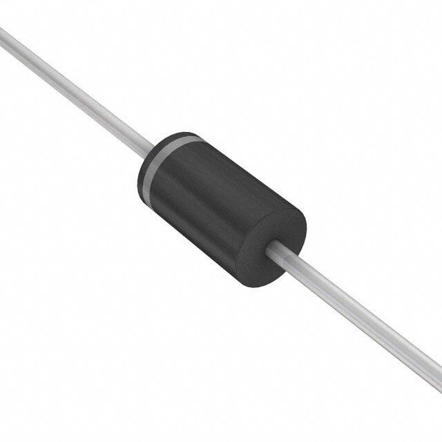
MCL103A, MCL103B, MCL103C www.vishay.com Vishay Semiconductors Small Signal Schottky Diodes FEATURES • Integrated protection ring against static discharge • Low capacitance • Low leakage current • Low forward voltage drop • AEC-Q101 qualified DESIGN SUPPORT TOOLS click logo to get started • Material categorization: for definitions of compliance please see www.vishay.com/doc?99912 APPLICATIONS Models Available • IHF-detector MECHANICAL DATA • Protection circuit Case: MicroMELF • Small battery charger Weight: approx. 12 mg • AC/DC / DC/DC converter for notebooks Cathode band color: black Packaging codes/options: TR3/10K per 13" reel (8 mm tape), 10K/box TR/2.5K per 7" reel (8 mm tape), 12.5K/box PARTS TABLE PART TYPE DIFFERENTIATION ORDERING CODE CIRCUIT CONFIGURATION REMARKS MCL103A V = 40 V MCL103A-TR3 or MCL103A-TR Single Tape and reel R MCL103B V = 30 V MCL103B-TR3 or MCL103B-TR Single Tape and reel R MCL103C V = 20 V MCL103C-TR3 or MCL103C-TR Single Tape and reel R ABSOLUTE MAXIMUM RATINGS (T = 25 °C, unless otherwise specified) amb PARAMETER TEST CONDITION PART SYMBOL VALUE UNIT MCL103A V 40 V R Reverse voltage MCL103B V 30 V R MCL103C V 20 V R Forward continuous current I 200 mA F Peak forward surge current t = 300 μs, square pulse I 15 A p FSM Power dissipation P 400 mW tot THERMAL CHARACTERISTICS (T = 25 °C, unless otherwise specified) amb PARAMETER TEST CONDITION SYMBOL VALUE UNIT On PC board Thermal resistance junction to ambient air R 250 K/W 50 mm x 50 mm x 1.6 mm thJA Junction temperature T 125 °C j Storage temperature range T -65 to +150 °C stg Rev. 1.7, 01-Jun-17 1 Document Number: 85632 For technical questions within your region: DiodesAmericas@vishay.com, DiodesAsia@vishay.com, DiodesEurope@vishay.com THIS DOCUMENT IS SUBJECT TO CHANGE WITHOUT NOTICE. THE PRODUCTS DESCRIBED HEREIN AND THIS DOCUMENT ARE SUBJECT TO SPECIFIC DISCLAIMERS, SET FORTH AT www.vishay.com/doc?91000
MCL103A, MCL103B, MCL103C www.vishay.com Vishay Semiconductors ELECTRICAL CHARACTERISTICS (T = 25 °C, unless otherwise specified) amb PARAMETER TEST CONDITION SYMBOL SYMBOL MIN. TYP. MAX. UNIT MCL103A V 40 V (BR) Reverse breakdown voltage I = 10 μA MCL103B V 30 V R (BR) MCL103C V 20 V (BR) V = 30 V MCL103A I 5 μA R R Leakage current V = 20 V MCL103B I 5 μA R R V = 10 V MCL103C I 5 μA R R I = 20 mA V 370 mV F F Forward voltage drop I = 200 mA V 600 mV F F Diode capacitance V = 0 V, f = 1 MHz C 50 pF R D I = I = 50 mA to 200 mA, Reverse recovery time F R t 10 ns recovery to 0.1 I rr R TYPICAL CHARACTERISTICS (T = 25 °C, unless otherwise specified) amb 1000 10 000 100 A) A) m µ 1000 Current ( 101 Current ( 100 I - Forward F 00.0.11 I - Reverse R 10 0.001 1 0 100 200 300 400 500 600 700 800900 1000 0 20 40 60 80 100 120 140 160 16767 T - Junction Temperature (°C) 16765 V - Forward Voltage (mV) j F Fig. 3 - Reverse Current vs. Junction Temperature Fig. 1 - Forward Current vs. Forward Voltage 5 30 f = 1 MHz nt (A) 4 e (pF) 25 Curre 3 citanc 20 ard apa 15 w 2 C or e F d 10 I - F 1 C - DioD 5 0 0 0.0 0.5 1.0 1.5 2.0 0 5 10 15 20 25 30 16766 V - Forward Voltage (V) F 16768 V - Reverse Voltage (V) R Fig. 2 - Forward Current vs. Forward Voltage Fig. 4 - Diode Capacitance vs. Reverse Voltage Rev. 1.7, 01-Jun-17 2 Document Number: 85632 For technical questions within your region: DiodesAmericas@vishay.com, DiodesAsia@vishay.com, DiodesEurope@vishay.com THIS DOCUMENT IS SUBJECT TO CHANGE WITHOUT NOTICE. THE PRODUCTS DESCRIBED HEREIN AND THIS DOCUMENT ARE SUBJECT TO SPECIFIC DISCLAIMERS, SET FORTH AT www.vishay.com/doc?91000
MCL103A, MCL103B, MCL103C www.vishay.com Vishay Semiconductors 25 A) 20 RepetitveCurrent ( 15 Non urge Typ. ard S 10 I - totForw 5 0 0.1 1.0 10.0 16769 t - Pulse width (ms) P Fig. 5 - Typical Non-Repetitive Forward Surge Current vs. Pulse Width PACKAGE DIMENSIONS in millimeters (inches): MicroMELF Cathode indification 1 (0.039) surface plan < 1.35 (g0l.a0s5s3) nalp ecafru s 7) 3) 4 4 0 0 0. 0. 2 ( 1 ( 1. 1. )4 2 * 0.25 (0.010) 0.0( 6 0.15 (0.006) .0 2 (0.079) > R2.5 (0.098) glass 1.8 (0.071) * The gap between plug and glass can be either on cathode or anode side Foot print recommendation: Reflow soldering Wave soldering 2.4 (0.094) 2.8 (0.110) 0.8 (0.031) 0.8 (0.031) 0.9 (0.035) 0.9 (0.035) 7) 0.04 055) 1.2 ( 4 (0. 1. 0.8 (0.031) 1 (0.039) Created - Date: 26.July.1996 Rev. 13 - Date: 07.June.2006 Document no.:6.560-5007.01-4 96 12072 Rev. 1.7, 01-Jun-17 3 Document Number: 85632 For technical questions within your region: DiodesAmericas@vishay.com, DiodesAsia@vishay.com, DiodesEurope@vishay.com THIS DOCUMENT IS SUBJECT TO CHANGE WITHOUT NOTICE. THE PRODUCTS DESCRIBED HEREIN AND THIS DOCUMENT ARE SUBJECT TO SPECIFIC DISCLAIMERS, SET FORTH AT www.vishay.com/doc?91000
Legal Disclaimer Notice www.vishay.com Vishay Disclaimer ALL PRODUCT, PRODUCT SPECIFICATIONS AND DATA ARE SUBJECT TO CHANGE WITHOUT NOTICE TO IMPROVE RELIABILITY, FUNCTION OR DESIGN OR OTHERWISE. Vishay Intertechnology, Inc., its affiliates, agents, and employees, and all persons acting on its or their behalf (collectively, “Vishay”), disclaim any and all liability for any errors, inaccuracies or incompleteness contained in any datasheet or in any other disclosure relating to any product. Vishay makes no warranty, representation or guarantee regarding the suitability of the products for any particular purpose or the continuing production of any product. To the maximum extent permitted by applicable law, Vishay disclaims (i) any and all liability arising out of the application or use of any product, (ii) any and all liability, including without limitation special, consequential or incidental damages, and (iii) any and all implied warranties, including warranties of fitness for particular purpose, non-infringement and merchantability. Statements regarding the suitability of products for certain types of applications are based on Vishay’s knowledge of typical requirements that are often placed on Vishay products in generic applications. Such statements are not binding statements about the suitability of products for a particular application. It is the customer’s responsibility to validate that a particular product with the properties described in the product specification is suitable for use in a particular application. Parameters provided in datasheets and / or specifications may vary in different applications and performance may vary over time. All operating parameters, including typical parameters, must be validated for each customer application by the customer’s technical experts. Product specifications do not expand or otherwise modify Vishay’s terms and conditions of purchase, including but not limited to the warranty expressed therein. Except as expressly indicated in writing, Vishay products are not designed for use in medical, life-saving, or life-sustaining applications or for any other application in which the failure of the Vishay product could result in personal injury or death. Customers using or selling Vishay products not expressly indicated for use in such applications do so at their own risk. Please contact authorized Vishay personnel to obtain written terms and conditions regarding products designed for such applications. No license, express or implied, by estoppel or otherwise, to any intellectual property rights is granted by this document or by any conduct of Vishay. Product names and markings noted herein may be trademarks of their respective owners. © 2017 VISHAY INTERTECHNOLOGY, INC. ALL RIGHTS RESERVED Revision: 08-Feb-17 1 Document Number: 91000
Mouser Electronics Authorized Distributor Click to View Pricing, Inventory, Delivery & Lifecycle Information: V ishay: MCL103C-TR MCL103A-TR MCL103A-TR3 MCL103B-TR MCL103B-TR3 MCL103C-TR3