ICGOO在线商城 > 集成电路(IC) > 嵌入式 - 微控制器 > MCF5372LCVM240

 Datasheet下载
- 型号: MCF5372LCVM240
- 制造商: Freescale Semiconductor
- 库位|库存: xxxx|xxxx
- 要求:
| 数量阶梯 | 香港交货 | 国内含税 |
| +xxxx | $xxxx | ¥xxxx |
查看当月历史价格
查看今年历史价格
MCF5372LCVM240产品简介:
ICGOO电子元器件商城为您提供MCF5372LCVM240由Freescale Semiconductor设计生产,在icgoo商城现货销售,并且可以通过原厂、代理商等渠道进行代购。 MCF5372LCVM240价格参考。Freescale SemiconductorMCF5372LCVM240封装/规格:嵌入式 - 微控制器, Coldfire V3 微控制器 IC MCF537x 32-位 240MHz ROMless 196-MAPBGA(15x15)。您可以下载MCF5372LCVM240参考资料、Datasheet数据手册功能说明书,资料中有MCF5372LCVM240 详细功能的应用电路图电压和使用方法及教程。
型号为MCF5372LCVM240的嵌入式微控制器由NXP USA Inc.生产,主要面向工业控制、通信设备和高性能嵌入式系统应用。该芯片基于ColdFire V4内核,主频高达240MHz,具备较强的处理能力和丰富的外设接口。

其主要应用场景包括:

1. 工业自动化与控制:用于PLC(可编程逻辑控制器)、电机控制、传感器网络等,支持实时控制与数据处理任务。

2. 通信设备:适用于路由器、交换机、无线基站控制器等网络设备,支持多协议通信和高速数据传输。

3. 人机界面(HMI):用于工业HMI、医疗设备显示终端等,支持图形界面显示和触摸控制。

4. 测试与测量仪器:适用于高精度测量设备,如示波器、分析仪等,提供快速数据采集与处理能力。

5. 楼宇自动化与安防系统:用于智能楼宇控制、门禁系统、视频监控设备等,支持多任务处理与实时响应。

该微控制器具备良好的环境适应性和稳定性,适合在工业级温度范围内运行,广泛应用于对性能和可靠性要求较高的嵌入式领域。
| 参数 | 数值 |
| 产品目录 | 集成电路 (IC)半导体 |
| 描述 | IC MCU 32BIT ROMLESS 196MAPBGA微处理器 - MPU MCF5329 V2-CORE |
| EEPROM容量 | - |
| 产品分类 | |
| I/O数 | 62 |
| L1CacheInstruction/DataMemory | 16 kB, 16 kB |
| L1缓存指令/数据存储器 | 16 kB, 16 kB |
| 品牌 | Freescale Semiconductor |
| 产品手册 | |
| 产品图片 |
|
| rohs | 符合RoHS无铅 / 符合限制有害物质指令(RoHS)规范要求 |
| 产品系列 | 嵌入式处理器和控制器,微处理器 - MPU,Freescale Semiconductor MCF5372LCVM240MCF537x |
| 数据手册 | |
| 产品型号 | MCF5372LCVM240 |
| RAM容量 | 32K x 8 |
| 产品培训模块 | http://www.digikey.cn/PTM/IndividualPTM.page?site=cn&lang=zhs&ptm=12511 |
| 产品种类 | 微处理器 - MPU |
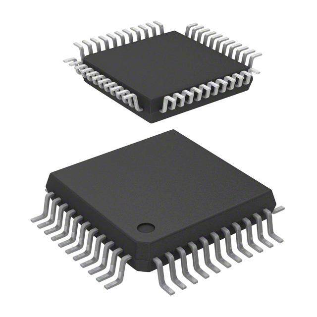
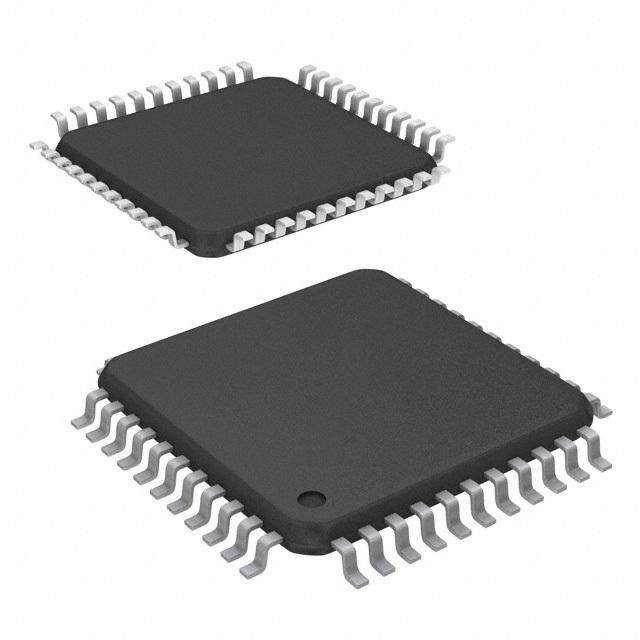
| 供应商器件封装 | 196-MAPBGA(15x15) |
| 包装 | 托盘 |
| 单位重量 | 482.550 mg |
| 商标 | Freescale Semiconductor |
| 商标名 | ColdFire |
| 外设 | DMA,POR,PWM,WDT |
| 安装风格 | SMD/SMT |
| 封装 | Tray |
| 封装/外壳 | 196-LBGA |
| 封装/箱体 | MABGA |
| 工作温度 | -40°C ~ 85°C |
| 工作电源电压 | 1.8 V, 2.5 V, 3.3 V |
| 工厂包装数量 | 630 |
| 振荡器类型 | 外部 |
| 数据RAM大小 | 32 kB |
| 数据总线宽度 | 32 bit |
| 数据转换器 | - |
| 最大工作温度 | + 105 C |
| 最大时钟频率 | 240 MHz |
| 最小工作温度 | - 40 C |
| 标准包装 | 630 |
| 核心 | ColdFire V3 |
| 核心处理器 | Coldfire V3 |
| 核心尺寸 | 32-位 |
| 电压-电源(Vcc/Vdd) | 1.4 V ~ 3.6 V |
| 程序存储器类型 | ROMless |
| 程序存储容量 | - |
| 系列 | MCF537X |
| 连接性 | EBI/EMI, 以太网, I²C, SPI, SSI, UART/USART, USB, USB OTG |
| 速度 | 240MHz |


PDF Datasheet 数据手册内容提取
Freescale Semiconductor Document Number: MCF5373DS Data Sheet: Technical Data Rev. 4, 11/2008 MCF5373 MAPBGA–256 MAPBGA–196 17mm x 17mm 15mm x 15mm ® MCF537x ColdFire QFP–160 28mm x 28mm Microprocessor Data Sheet Features • Version 3 ColdFire variable-length RISC processor core • System debug support • JTAG support for system level board testing • On-chip memories – 16-Kbyte unified write-back cache – 32-Kbyte dual-ported SRAM on CPU internal bus, accessible by core and non-core bus masters (e.g., DMA, FEC, and USB host and OTG) • Power management • Embedded Voice-over-IP (VoIP) system solution • SDR/DDR SDRAM Controller • Universal Serial Bus (USB) Host Controller • Universal Serial Bus (USB) On-the-Go (OTG) controller • Synchronous Serial Interface (SSI) • Fast Ethernet Controller (FEC) • Cryptography Hardware Accelerators • FlexCAN Module • Three Universal Asynchronous Receiver Transmitters (UARTs) • I2C Module • Queued Serial Peripheral Interface (QSPI) • Pulse Width Modulation (PWM) module • Real Time Clock • Four 32-bit DMA Timers • Software Watchdog Timer • Four Periodic Interrupt Timers (PITs) • Phase Locked Loop (PLL) • Interrupt Controllers (x2) • DMA Controller • FlexBus (External Interface) • Chip Configuration Module (CCM) • Reset Controller • General Purpose I/O interface ©Freescale Semiconductor, Inc., 2008. All rights reserved.
Table of Contents 1 MCF537x Family Comparison . . . . . . . . . . . . . . . . . . . . . . . . .3 5.7.1 SDR SDRAM AC Timing Characteristics. . . . . 21 2 Ordering Information. . . . . . . . . . . . . . . . . . . . . . . . . . . . . . . . .4 5.7.2 DDR SDRAM AC Timing Characteristics. . . . . 23 3 Hardware Design Considerations. . . . . . . . . . . . . . . . . . . . . . .5 5.8 General Purpose I/O Timing . . . . . . . . . . . . . . . . . . . . 26 3.1 PLL Power Filtering. . . . . . . . . . . . . . . . . . . . . . . . . . . . .5 5.9 Reset and Configuration Override Timing. . . . . . . . . . 27 3.2 USB Power Filtering . . . . . . . . . . . . . . . . . . . . . . . . . . . .5 5.10 USB On-The-Go . . . . . . . . . . . . . . . . . . . . . . . . . . . . . 28 3.3 Supply Voltage Sequencing and Separation Cautions . .5 5.11 SSI Timing Specifications . . . . . . . . . . . . . . . . . . . . . . 28 3.3.1 Power Up Sequence . . . . . . . . . . . . . . . . . . . . . .5 5.12 I2C Input/Output Timing Specifications . . . . . . . . . . . . 29 3.3.2 Power Down Sequence. . . . . . . . . . . . . . . . . . . .6 5.13 Fast Ethernet AC Timing Specifications . . . . . . . . . . . 31 4 Pin Assignments and Reset States . . . . . . . . . . . . . . . . . . . . .6 5.13.1 MII Receive Signal Timing . . . . . . . . . . . . . . . . 31 4.1 Signal Multiplexing . . . . . . . . . . . . . . . . . . . . . . . . . . . . .6 5.13.2 MII Transmit Signal Timing. . . . . . . . . . . . . . . . 31 4.2 Pinout—196 MAPBGA . . . . . . . . . . . . . . . . . . . . . . . . .12 5.13.3 MII Async Inputs Signal Timing . . . . . . . . . . . . 32 4.3 Pinout—160 QFP . . . . . . . . . . . . . . . . . . . . . . . . . . . . .13 5.13.4 MII Serial Management Channel Timing . . . . . 32 5 Electrical Characteristics . . . . . . . . . . . . . . . . . . . . . . . . . . . .14 5.14 32-Bit Timer Module Timing Specifications. . . . . . . . . 33 5.1 Maximum Ratings. . . . . . . . . . . . . . . . . . . . . . . . . . . . .14 5.15 QSPI Electrical Specifications. . . . . . . . . . . . . . . . . . . 33 5.2 Thermal Characteristics . . . . . . . . . . . . . . . . . . . . . . . .15 5.16 JTAG and Boundary Scan Timing. . . . . . . . . . . . . . . . 34 5.3 ESD Protection. . . . . . . . . . . . . . . . . . . . . . . . . . . . . . .16 5.17 Debug AC Timing Specifications. . . . . . . . . . . . . . . . . 36 5.4 DC Electrical Specifications . . . . . . . . . . . . . . . . . . . . .16 6 Current Consumption . . . . . . . . . . . . . . . . . . . . . . . . . . . . . . 36 5.5 Oscillator and PLL Electrical Characteristics . . . . . . . .17 7 Package Information . . . . . . . . . . . . . . . . . . . . . . . . . . . . . . . 39 5.6 External Interface Timing Characteristics. . . . . . . . . . .18 7.1 Package Dimensions—196 MAPBGA. . . . . . . . . . . . . 40 5.6.1 FlexBus . . . . . . . . . . . . . . . . . . . . . . . . . . . . . . .19 7.2 Package Dimensions—160 QFP. . . . . . . . . . . . . . . . . 41 5.7 SDRAM Bus . . . . . . . . . . . . . . . . . . . . . . . . . . . . . . . . .21 8 Revision History . . . . . . . . . . . . . . . . . . . . . . . . . . . . . . . . . . 43 MCF537x ColdFire® Microprocessor Data Sheet, Rev. 4 2 Freescale Semiconductor
MCF537x Family Comparison USB OTG (To/From SRAM backdoor) FlexBus Chip Selects USB OTG USB Host M5 M6 S4 S1 SDRAMC USB Host XBS External SDRAMC Interface QSPI M2 I2C M1 S7 M0 S6 Cryptography UART Modules INTC0 SDRAMC RNGA ng PWM xi DMA Timer (To/From PADI) SKHA u FEC INTC1 n M FEC MDHA Pi CANRX — CANTX DI A SSI P DMA Timers FlexCAN1 I2C QSPI UARTs DREQn DACKn (To/From PADI) DMA D[31:0] A[23:0] R/W DIV EMAC M CS[5:0] V3 ColdFire CPU BD TA TS R BE/BWE[3:0] V C USB OTG X PORTS (To/From PADI) XCVR USB Host SDRAMC 1 6C KacBhyete TTTTRCMDSLISKT JTTAAPG PWMs, EPORT, (1024x32)x4 TDO Watchdog, PITs SSI RESET RCON Reset 32 KByte JTAG_EN RSTOUT SRAM PLL RTC (4096x32)x2 T K Note: LKOU XTAL TAL TAL32 AL32K (To/From XBS) 1 FMleCxFC5A3N72 i1s doenvlyic oen the C E X X T E X Figure1. MCF5373 Block Diagram 1 MCF537x Family Comparison The following table compares the various device derivatives available within the MCF537x family. Table1. MCF537x Family Configurations Module MCF5372 MCF5372L MCF53721 MCF5373 MCF5373L ColdFire Version 3 Core with EMAC (cid:129) (cid:129) (cid:129) (cid:129) (cid:129) (Enhanced Multiply-Accumulate Unit) Core (System) Clock up to up to up to up to 240MHz 180MHz 180MHz 240MHz Peripheral and External Bus Clock up to up to up to up to 80MHz (Core clock ÷ 3) 60MHz 60MHz 80MHz Performance (Dhrystone/2.1 MIPS) up to 158 up to 211 up to 158 up to 211 Instruction/Data Cache 16 Kbytes MCF537x ColdFire® Microprocessor Data Sheet, Rev. 4 Freescale Semiconductor 3
Ordering Information Table1. MCF537x Family Configurations (continued) Module MCF5372 MCF5372L MCF53721 MCF5373 MCF5373L Static RAM (SRAM) 32 Kbytes SDR/DDR SDRAM Controller (cid:129) (cid:129) (cid:129) (cid:129) (cid:129) USB 2.0 Host — (cid:129) (cid:129) — (cid:129) USB 2.0 On-the-Go — (cid:129) (cid:129) — (cid:129) Synchronous Serial Interface (SSI) (cid:129) (cid:129) (cid:129) (cid:129) (cid:129) Fast Ethernet Controller (FEC) (cid:129) (cid:129) (cid:129) (cid:129) (cid:129) Cryptography Hardware Accelerators — — — (cid:129) (cid:129) Embedded Voice-over-IP System Solution — — (cid:129) — — FlexCAN 2.0B communication module — — (cid:129) — — UARTs 3 3 3 3 3 I2C (cid:129) (cid:129) (cid:129) (cid:129) (cid:129) QSPI (cid:129) (cid:129) (cid:129) (cid:129) (cid:129) PWM Module — (cid:129) (cid:129) — (cid:129) Real Time Clock (cid:129) (cid:129) (cid:129) (cid:129) (cid:129) 32-bit DMA Timers 4 4 4 4 4 Watchdog Timer (WDT) (cid:129) (cid:129) (cid:129) (cid:129) (cid:129) Periodic Interrupt Timers (PIT) 4 4 4 4 4 Edge Port Module (EPORT) (cid:129) (cid:129) (cid:129) (cid:129) (cid:129) Interrupt Controllers (INTC) 2 2 2 2 2 16-channel Direct Memory Access (DMA) (cid:129) (cid:129) (cid:129) (cid:129) (cid:129) FlexBus External Interface (cid:129) (cid:129) (cid:129) (cid:129) (cid:129) General Purpose I/O (GPIO) up to 46 up to 62 up to 62 up to 46 up to 62 JTAG - IEEE® 1149.1 Test Access Port (cid:129) (cid:129) (cid:129) (cid:129) (cid:129) Package 160 196 196 160 196 QFP MAPBGA MAPBGA QFP MAPBGA 2 Ordering Information Table2. Orderable Part Numbers Freescale Part Description Package Speed Temperature Number MCF5372CAB180 MCF5372 RISC Microprocessor 160 QFP 180 MHz –40° to +85° C MCF5372LCVM240 MCF5372 RISC Microprocessor 196 MAPBGA 240 MHz –40° to +85° C MCF53721CVM240 MCF53721 RISC Microprocessor 196 MAPBGA 240 MHz –40° to +85° C MCF5373CAB180 MCF5373 RISC Microprocessor 160 QFP 180 MHz –40° to +85° C MCF5373LCVM240 MCF5373 RISC Microprocessor 196 MAPBGA 240 MHz –40° to +85° C MCF537x ColdFire® Microprocessor Data Sheet, Rev. 4 4 Freescale Semiconductor
Hardware Design Considerations 3 Hardware Design Considerations 3.1 PLL Power Filtering To further enhance noise isolation, an external filter is strongly recommended for PLL analog V pins. The filter shown in DD Figure2 should be connected between the board V and the PLLV pins. The resistor and capacitors should be placed as DD DD close to the dedicated PLLV pin as possible. DD 10 Ω Board IV PLL V Pin DD DD 10 µF 0.1 µF GND Figure2. System PLL V Power Filter DD 3.2 USB Power Filtering To minimize noise, external filters are required for each of the USB power pins. The filter shown in Figure3 should be connected between the board EV or IV and each of the USBV pins. The resistor and capacitors should be placed as DD DD DD close to the dedicated USBV pin as possible. DD 0 Ω Board EV USB V Pin DD DD 10 µF 0.1 µF GND Figure3. USB V Power Filter DD NOTE In addition to the above filter circuitry, a 0.01F capacitor is also recommended in parallel with those shown. 3.3 Supply Voltage Sequencing and Separation Cautions The relationship between SDV and EV is non-critical during power-up and power-down sequences. SDV (2.5V or DD DD DD 3.3V) and EV are specified relative to IV . DD DD 3.3.1 Power Up Sequence If EV /SDV are powered up with IV at 0V, the sense circuits in the I/O pads cause all pad output drivers connected to DD DD DD the EV /SDV to be in a high impedance state. There is no limit on how long after EV /SDV powers up before IV DD DD DD DD DD must powered up. IV should not lead the EV , SDV , or PLLV by more than 0.4V during power ramp-up or there is DD DD DD DD MCF537x ColdFire® Microprocessor Data Sheet, Rev. 4 Freescale Semiconductor 5
Pin Assignments and Reset States high current in the internal ESD protection diodes. The rise times on the power supplies should be slower than 500us to avoid turning on the internal ESD protection clamp diodes. 3.3.2 Power Down Sequence If IV /PLLV are powered down first, sense circuits in the I/O pads cause all output drivers to be in a high impedance state. DD DD There is no limit on how long after IV and PLLV power down before EV or SDV must power down. IV should DD DD DD DD DD not lag EV , SDV , or PLLV going low by more than 0.4V during power down or there is undesired high current in the DD DD DD ESD protection diodes. There are no requirements for the fall times of the power supplies. The recommended power down sequence is as follows: 1. Drop IV /PLLV to 0V. DD DD 2. Drop EV /SDV supplies. DD DD 4 Pin Assignments and Reset States 4.1 Signal Multiplexing The following table lists all the MCF537x pins grouped by function. The Dir column is the direction for the primary function of the pin only. Refer to Section7, “Package Information,” for package diagrams. For a more detailed discussion of the MCF537x signals, consult the MCF5373 Reference Manual (MCF5373RM). NOTE In this table and throughout this document, a single signal within a group is designated without square brackets (i.e., A23), while designations for multiple signals within a group use brackets (i.e., A[23:21]) and is meant to include all signals within the two bracketed numbers when these numbers are separated by a colon. NOTE The primary functionality of a pin is not necessarily its default functionality. Pins that are muxed with GPIO default to their GPIO functionality. Table3. MCF5372/3 Signal Information and Muxing MCF5372L en MCF5372 Signal Name GPIO Alternate 1 Alternate 2 1Dir. oltagomai M16C0F Q53F7P3 MMCCFF55337732L1 VD 196 MAPBGA Reset RESET2 — — — I EVDD 95 K13 RSTOUT — — — O EVDD 86 L12 Clock EXTAL — — — I EVDD 91 L14 XTAL2 — — — O EVDD 93 K14 EXTAL32K — — — I EVDD — P13 XTAL32K — — — O EVDD — N13 FB_CLK — — — O SDVDD 40 N1 MCF537x ColdFire® Microprocessor Data Sheet, Rev. 4 6 Freescale Semiconductor
Pin Assignments and Reset States Table3. MCF5372/3 Signal Information and Muxing (continued) MCF5372L en MCF5372 Signal Name GPIO Alternate 1 Alternate 2 1Dir. oltagomai M16C0F Q53F7P3 MMCCFF55337732L1 VD 196 MAPBGA Mode Selection RCON2 — — — I EVDD 72 P8 DRAMSEL — — — I EVDD 92 J11 FlexBus A[23:22] — FB_CS[5:4] — O SDVDD 134, 133 A9, B9 A[21:16] — — — O SDVDD 132–127 C9, D9, A10, B10, C10, D10 A[15:14] — SD_BA[1:0]3 — O SDVDD 126, 123 A11, B11 A[13:11] — SD_A[13:11]3 — O SDVDD 120–118 C11, A12, B12 A10 — — — O SDVDD 11 7 A13 A[9:0] — SD_A[9:0]3 — O SDVDD 116–107 A14, B14, B13, C12, D11, C14, C13, D14–D12 D[31:16] — SD_D[31:16]4 — I/O SDVDD 27–34, 46–53 J2, J1, K4–K1, L4, L3, N2, P1, P2, N3, L5, P3, N4, P4 D[15:1] — FB_D[31:17]4 — I/O SDVDD 16–23, 57–63 F2, F1, G4–G1, H4, H3, L6, M6, N6, P6, L7, M7, N7 D02 — FB_D[16]4 — I/O SDVDD 64 P7 BE/BWE[3:0] PBE[3:0] SD_DQM[3:0]3 — O SDVDD 26, 54, 24, 56 J3, M5, H2, P5 OE PBUSCTL3 — — O SDVDD 66 M8 TA2 PBUSCTL2 — — I SDVDD 106 E14 R/W PBUSCTL1 — — O SDVDD 65 L8 TS PBUSCTL0 DACK0 — O SDVDD 12 E2 Chip Selects FB_CS[5:4] PCS[5:4] — — O SDVDD — D8, C8 FB_CS[3:2] PCS[3:2] — — O SDVDD — B8, A8 FB_CS1 PCS1 — — O SDVDD 135 D7 FB_CS0 — — — O SDVDD 136 C7 SDRAM Controller SD_A10 — — — O SDVDD 43 M2 SD_CKE — — — O SDVDD 14 F4 MCF537x ColdFire® Microprocessor Data Sheet, Rev. 4 Freescale Semiconductor 7
Pin Assignments and Reset States Table3. MCF5372/3 Signal Information and Muxing (continued) MCF5372L en MCF5372 Signal Name GPIO Alternate 1 Alternate 2 1Dir. oltagomai M16C0F Q53F7P3 MMCCFF55337732L1 VD 196 MAPBGA SD_CLK — — — O SDVDD 37 L1 SD_CLK — — — O SDVDD 38 M1 SD_CS0 — — — O SDVDD 15 F3 SD_DQS3 — — — O SDVDD 25 H1 SD_DQS2 — — — O SDVDD 55 N5 SD_SCAS — — — O SDVDD 44 M3 SD_SRAS — — — O SDVDD 45 M4 SD_SDR_DQS — — — O SDVDD 35 L2 SD_WE — — — O SDVDD 13 E1 External Interrupts Port5 IRQ72 PIRQ72 — — I EVDD 102 F13 IRQ62 PIRQ62 USBHOST_ — I EVDD — F12 VBUS_EN IRQ52 PIRQ52 USBHOST_ — I EVDD — F11 VBUS_OC IRQ42 PIRQ42 SSI_MCLK — I EVDD 101 G14 IRQ32 PIRQ32 — — I EVDD — G13 IRQ22 PIRQ22 USB_CLKIN — I EVDD — G12 IRQ12 PIRQ12 DREQ12 SSI_CLKIN I EVDD 100 G11 FEC FEC_MDC PFECI2C3 I2C_SCL2 — O EVDD 4 B1 FEC_MDIO PFECI2C2 I2C_SDA2 — I/O EVDD 3 A1 FEC_COL PFECH7 — — I EVDD 144 B6 FEC_CRS PFECH6 — — I EVDD 145 A6 FEC_RXCLK PFECH5 — — I EVDD 146 A5 FEC_RXDV PFECH4 — — I EVDD 147 B5 FEC_RXD[3:0] PFECH[3:0] — — I EVDD 148–151 C5, D5, A4, B4 FEC_RXER PFECL7 — — I EVDD 152 C4 FEC_TXCLK PFECL6 — — I EVDD 153 A3 FEC_TXEN PFECL5 — — O EVDD 154 B3 FEC_TXER PFECL4 — — O EVDD 155 A2 FEC_TXD[3:0] PFECL[3:0] — — O EVDD 157, 158, 1, 2 D4, C3, B2, C2 MCF537x ColdFire® Microprocessor Data Sheet, Rev. 4 8 Freescale Semiconductor
Pin Assignments and Reset States Table3. MCF5372/3 Signal Information and Muxing (continued) MCF5372L en MCF5372 Signal Name GPIO Alternate 1 Alternate 2 1Dir. oltagomai M16C0F Q53F7P3 MMCCFF55337732L1 VD 196 MAPBGA USB Host & USB On-the-Go USBOTG_M — — — I/O USB — H14 VDD USBOTG_P — — — I/O USB — H13 VDD USBHOST_M — — — I/O USB — J13 VDD USBHOST_P — — — I/O USB — J12 VDD FlexCAN (MCF53721 only) CANRX and CANTX do not have dedicated bond pads. Please refer to the following pins for muxing: I2C_SDA for CANRX and I2C_SCL for CANTX. PWM PWM7 PPWM7 — — I/O EVDD — E13 PWM5 PPWM5 — — I/O EVDD — E12 PWM3 PPWM3 DT3OUT DT3IN I/O EVDD — E11 PWM1 PPWM1 DT2OUT DT2IN I/O EVDD — F14 SSI The SSI signals do not have dedicated bond pads. Please refer to the following pins for muxing: IRQ4 for SSI_MCLK, IRQ1 for SSI_CLKIN, U1CTS for SSI_BCLK, U1RTS for SSI_FS, U1RXD for SSI_RXD, and U1TXD for SSI_TXD I2C I2C_SCL2 PFECI2C1 CANTX6 U2TXD I/O EVDD — E3 I2C_SDA2 PFECI2C0 CANRX6 U2RXD I/O EVDD — E4 DMA DACK[1:0] and DREQ[1:0] do not have dedicated bond pads. Please refer to the following pins for muxing: TS for DACK0, DT0IN for DREQ0, DT1IN for DACK1, and IRQ1 for DREQ1. QSPI QSPI_CS2 PQSPI5 U2RTS — O EVDD 78 N12 QSPI_CS1 PQSPI4 PWM7 USBOTG_ O EVDD — M12 PU_EN QSPI_CS0 PQSPI3 PWM5 — O EVDD — M11 QSPI_CLK PQSPI2 I2C_SCL2 — O EVDD 77 P12 QSPI_DIN PQSPI1 U2CTS — I EVDD 75 P11 QSPI_DOUT PQSPI0 I2C_SDA2 — O EVDD 76 N11 MCF537x ColdFire® Microprocessor Data Sheet, Rev. 4 Freescale Semiconductor 9
Pin Assignments and Reset States Table3. MCF5372/3 Signal Information and Muxing (continued) MCF5372L en MCF5372 Signal Name GPIO Alternate 1 Alternate 2 1Dir. oltagomai M16C0F Q53F7P3 MMCCFF55337732L1 VD 196 MAPBGA UARTs U1CTS PUARTL7 SSI_BCLK — I EVDD 143 C6 U1RTS PUARTL6 SSI_FS — O EVDD 142 D6 U1TXD PUARTL5 SSI_TXD2 — O EVDD 141 A7 U1RXD PUARTL4 SSI_RXD2 — I EVDD 140 B7 U0CTS PUARTL3 — — I EVDD 85 M14 U0RTS PUARTL2 — — O EVDD 84 M13 U0TXD PUARTL1 — — O EVDD 83 N14 U0RXD PUARTL0 — — I EVDD 80 P14 Note:The UART2 signals are multiplexed on the QSPI, DMA Timers, and I2C pins. DMA Timers DT3IN PTIMER3 DT3OUT U2RXD I EVDD 8 D1 DT2IN PTIMER2 DT2OUT U2TXD I EVDD 7 C1 DT1IN PTIMER1 DT1OUT DACK1 I EVDD 6 D2 DT0IN PTIMER0 DT0OUT DREQ02 I EVDD 5 D3 BDM/JTAG7 JTAG_EN8 — — — I EVDD 96 G10 DSCLK — TRST2 — I EVDD 88 K11 PSTCLK — TCLK2 — O EVDD 70 N8 BKPT — TMS2 — I EVDD 87 L13 DSI — TDI2 — I EVDD 90 K12 DSO — TDO — O EVDD 74 L11 DDATA[3:0] — — — O EVDD — L9, M9, N9, P9 PST[3:0] — — — O EVDD — L10, M10, N10, P10 ALLPST — — — O EVDD 73 — MCF537x ColdFire® Microprocessor Data Sheet, Rev. 4 10 Freescale Semiconductor
Pin Assignments and Reset States Table3. MCF5372/3 Signal Information and Muxing (continued) MCF5372L en MCF5372 Signal Name GPIO Alternate 1 Alternate 2 1Dir. oltagomai M16C0F Q53F7P3 MMCCFF55337732L1 VD 196 MAPBGA Test TEST8 — — — I EVDD 124 E10 Power Supplies EVDD — — — — — 9, 69, 71, 81, 94, E6, E7, F5–F7, 103, 139, 160 G5, H10, J8, K8–K9 IVDD — — — — — 36, 79, 97, 125, E5, J9, K5, K10 156 PLL_VDD — — — — — 99 J10 SD_VDD — — — — — 11, 39, 41, 67, E8–E9, F8–F10, 105, 121, 137 J4–J7, H5, K6, K7 USB_VDD — — — — — — H12 VSS — — — — — 10, 42, 68, 82, G6–G9, H6–H9 89, 104, 122, 138, 159 PLL_VSS — — — — — 98 H11 USB_VSS — — — — — — J14 1 Refers to pin’s primary function. 2 Pull-up enabled internally on this signal for this mode. 3 The SDRAM functions of these signals are not programmable by the user. They are dynamically switched by the processor when accessing SDRAM memory space and are included here for completeness. 4 Primary functionality selected by asserting the DRAMSEL signal (SDR mode). Alternate functionality selected by negating the DRAMSEL signal (DDR mode). The GPIO module is not responsible for assigning these pins. 5 GPIO functionality is determined by the edge port module. The GPIO module is only responsible for assigning the alternate functions. 6 MCF53721 only. 7 If JTAG_EN is asserted, these pins default to Alternate 1 (JTAG) functionality. The GPIO module is not responsible for assigning these pins. 8 Pull-down enabled internally on this signal for this mode. NOTE MCF537x ColdFire® Microprocessor Data Sheet, Rev. 4 Freescale Semiconductor 11
Pin Assignments and Reset States 4.2 Pinout—196 MAPBGA The pinout for the MCF5373LCVM240, MCF5372LCVM240, and MCF53721CVM240 packages are shown below. 1 2 3 4 5 6 7 8 9 10 11 12 13 14 A FEC_ FEC_ FEC_ FEC_ FEC_ FEC_ A U1TXD FB_CS2 A23 A19 A15 A12 A10 A9 MDIO TXER TXCLK RXD1 RXCLK CRS B FEC_ FEC_ FEC_ FEC_ FEC_ FEC_ B U1RXD FB_CS3 A22/ A18 A14 A11 A7 A8 MDC TXD1 TXEN RXD0 RXDV COL C FEC_ FEC_ FEC_ FEC_ C DT2IN U1CTS FB_CS0 FB_CS4 A21 A17 A13 A6 A3 A4 TXD0 TXD2 RXER RXD3 D FEC_ FEC_ D DT3IN DT1IN DT0IN U1RTS FB_CS1 FB_CS5 A20 A16 A5 A0 A1 A2 TXD3 RXD2 E E SD_WE TS I2C_SCL I2C_SDA IVDD EVDD EVDD SD_VDD SD_VDD TEST PWM3 PWM5 PWM7 TA F F D14 D15 SD_CS0 SD_CKE EVDD EVDD EVDD SD_VDD SD_VDD SD_VDD IRQ5 IRQ6 IRQ7 PWM1 G JTAG_ G D10 D11 D12 D13 EVDD VSS VSS VSS VSS IRQ1 IRQ2 IRQ3 IRQ4 EN H SD_ BE/ PLL_ USBOTG USB USB H D8 D9 SD_VDD VSS VSS VSS VSS EVDD DQS3 BWE1 VSS _VDD OTG_P OTG_M J BE/ PLL_ DRAM USB USB USBHOST J D30 D31 SD_VDD SD_VDD SD_VDD SD_VDD EVDD IVDD BWE3 VDD SEL HOST_P HOST_M _VSS K TRST/ K D26 D27 D28 D29 IVDD SD_VDD SD_VDD EVDD EVDD IVDD TDI/DSI RESET XTAL DSCLK L SD_DR_ TDO/ TMS/ L SD_CLK D24 D25 D19 D7 D3 R/W DDATA3 PST3 RSTOUT EXTAL DQS DSO BKPT M BE/ QSPI_ QSPI_ M SD_CLK SD_A10 SD_CAS SD_RAS D6 D2 OE DDATA2 PST2 U0RTS U0CTS BWE2 CS0 CS1 N SD_ TCLK/ QSPI_ QSPI_ XTAL N FB_CLK D23 D20 D17 D5 D1 DDATA1 PST1 U0TXD DQS2 PSTCLK DOUT CS2 32K P BE/ QSPI_ QSPI_ EXTAL P D22 D21 D18 D16 D4 D0 RCON DDATA0 PST0 U0RXD BWE0 DIN CLK 32K 1 2 3 4 5 6 7 8 9 10 11 12 13 14 Figure4. MCF5373LCVM240, MCF5372LCVM240, and MCF53721CVM240 Pinout Top View (196 MAPBGA) MCF537x ColdFire® Microprocessor Data Sheet, Rev. 4 12 Freescale Semiconductor
Pin Assignments and Reset States 4.3 Pinout—160 QFP The pinout for the MCF5372CAB180 and MCF5373CAB180 packages is shown below. K K 5 4 2 3 R N L R 0 1 2 3 V L S S D D E E C E D D D D D C S L C C EVDD VSS FEC_TX FEC_TX IVDD FEC_TX FEC_TX FEC_TX FEC_RX FEC_RX FEC_RX FEC_RX FEC_RX FEC_RX FEC_RX FEC_CR FEC_CO U1CTS U1RTS U1TXDU1RXD EVDD VSS SD_VDD FB_CS0 FB_CS1 A23/FB_ A22/FB_ A21 A20A19 A18 A17 A16 A15 IVDD TEST A14 VSSSD_VDD (cid:129) 0 9 8 7 6 5 4 3 2 1 0 9 8 7 6 5 4 3 2 1 0 9 8 7 6 5 4 3 2 1 0 9 8 7 6 5 4 3 2 1 6 5 5 5 5 5 5 5 5 5 5 4 4 4 4 4 4 4 4 4 4 3 3 3 3 3 3 3 3 3 3 2 2 2 2 2 2 2 2 2 1 1 1 1 1 1 1 1 1 1 1 1 1 1 1 1 1 1 1 1 1 1 1 1 1 1 1 1 1 1 1 1 1 1 1 1 1 1 1 1 FEC_TXD1 1 120 A13 FEC_TXD0 2 119 A12 FEC_MDIO 3 118 A11 FEC_MDC 4 117 A10 DT0IN 5 116 A9 DT1IN 6 115 A8 DT2IN 7 114 A7 DT3IN 8 113 A6 EVDD 9 112 A5 VSS 10 111 A4 SD_VDD 11 110 A3 TS 12 109 A2 SD_WE 13 108 A1 SD_CKE 14 107 A0 SD_CS0 15 106 TA D15 16 105 SD_VDD D14 17 104 VSS D13 18 103 EVDD D12 19 102 IRQ7 D11 20 101 IRQ4 D10 21 100 IRQ1 D9 22 99 PLL_VDD D8 23 98 PLL_VSS BE/BWE1 24 97 IVDD SD_DQS1/3 25 96 JTAG_EN BE/BWE3 26 95 RESET D31 27 94 EVDD D30 28 93 XTAL D29 29 92 DRAMSEL D28 30 91 EXTAL D27 31 90 TDI/DSI D26 32 89 VSS D25 33 88 TRST/DSCLK D24 34 87 TMS/BKPT SD_DR_DQS 35 86 RSTOUT IVDD 36 85 U0CTS SD_CLK 37 84 U0RTS SD_CLK 38 83 U0TXD SD_VDD 39 82 VSS FB_CLK 40 81 EVDD 1 2 3 4 5 6 7 8 9 0 1 2 3 4 5 6 7 8 9 0 1 2 3 4 5 6 7 8 9 0 1 2 3 4 5 6 7 8 9 0 4 4 4 4 4 4 4 4 4 5 5 5 5 5 5 5 5 5 5 6 6 6 6 6 6 6 6 6 6 7 7 7 7 7 7 7 7 7 7 8 D S 0 S S 3 2 1 0 9 8 7 62 2 0 7 6 5 4 3 2 1 0 W E D S D K D N T O N T K 2 DD SD_VD VS SD_A1 SD_CA SD_RA D2 D2 D2 D2 D1 D1 D1 D1BE/BWE D_DQS0/ BE/BWE D D D D D D D D R/ O SD_VD VS EVD K/PSTCL EVD RCO ALL_PS TDO/DS QSPI_DI SPI_DOU QSPI_CL QSPI_CS IVDU0RX S CL Q T Figure5. MCF5372CAB180 and MCF5373CAB180 Pinout Top View (160 QFP) MCF537x ColdFire® Microprocessor Data Sheet, Rev. 4 Freescale Semiconductor 13
Electrical Characteristics 5 Electrical Characteristics This document contains electrical specification tables and reference timing diagrams for the MCF5373 microcontroller unit. This section contains detailed information on power considerations, DC/AC electrical characteristics, and AC timing specifications of MCF5373. The electrical specifications are preliminary and are from previous designs or design simulations. These specifications may not be fully tested or guaranteed at this early stage of the product life cycle. However, for production silicon, these specifications will be met. Finalized specifications will be published after complete characterization and device qualifications have been completed. NOTE The parameters specified in this MCU document supersede any values found in the module specifications. 5.1 Maximum Ratings Table4. Absolute Maximum Ratings1, 2 Rating Symbol Value Unit Core Supply Voltage IV – 0.5 to +2.0 V DD CMOS Pad Supply Voltage EV – 0.3 to +4.0 V DD DDR/Memory Pad Supply Voltage SDV – 0.3 to +4.0 V DD PLL Supply Voltage PLLV – 0.3 to +2.0 V DD Digital Input Voltage 3 V – 0.3 to +3.6 V IN Instantaneous Maximum Current I 25 mA Single pin limit (applies to all pins) 3, 4, 5 D Operating Temperature Range (Packaged) T A – 40 to +85 °C (T - T ) L H Storage Temperature Range T – 55 to +150 °C stg 1 Functional operating conditions are given in Section5.4, “DC Electrical Specifications.” Absolute maximum ratings are stress ratings only, and functional operation at the maxima is not guaranteed. Continued operation at these levels may affect device reliability or cause permanent damage to the device. 2 This device contains circuitry protecting against damage due to high static voltage or electrical fields; however, it is advised that normal precautions be taken to avoid application of any voltages higher than maximum-rated voltages to this high-impedance circuit. Reliability of operation is enhanced if unused inputs are tied to an appropriate logic voltage level (V or SS EV ). DD 3 Input must be current limited to the value specified. To determine the value of the required current-limiting resistor, calculate resistance values for positive and negative clamp voltages, and then use the larger of the two values. 4 All functional non-supply pins are internally clamped to V and EV . SS DD 5 Power supply must maintain regulation within operating EV range during instantaneous and DD operating maximum current conditions. If positive injection current (V > EV ) is greater than in DD I , the injection current may flow out of EV and could result in external power supply going DD DD out of regulation. Ensure external EV load shunts current greater than maximum injection DD current. This is the greatest risk when the MCU is not consuming power (ex; no clock). Power supply must maintain regulation within operating EV range during instantaneous and DD operating maximum current conditions. MCF537x ColdFire® Microprocessor Data Sheet, Rev. 4 14 Freescale Semiconductor
Electrical Characteristics 5.2 Thermal Characteristics Table5. Thermal Characteristics Characteristic Symbol 256MBGA 196MBGA 160QFP Unit Junction to ambient, natural convection Four layer board θ 371,2 421,2 491,2 °C / W (2s2p) JMA Junction to ambient (@200 ft/min) Four layer board θ 341,2 381,2 441,2 °C / W (2s2p) JMA Junction to board θ 273 323 403 °C / W JB Junction to case θ 164 194 394 °C / W JC Junction to top of package Ψ 41,5 51,5 121,5 °C / W jt Maximum operating junction temperature T 105 105 105 oC j 1 θ and Ψ parameters are simulated in conformance with EIA/JESD Standard 51-2 for natural convection. Freescale JMA jt recommends the use of θ and power dissipation specifications in the system design to prevent device junction JmA temperatures from exceeding the rated specification. System designers should be aware that device junction temperatures can be significantly influenced by board layout and surrounding devices. Conformance to the device junction temperature specification can be verified by physical measurement in the customer’s system using the Ψ parameter, the device power jt dissipation, and the method described in EIA/JESD Standard 51-2. 2 Per JEDEC JESD51-6 with the board horizontal. 3 Thermal resistance between the die and the printed circuit board in conformance with JEDEC JESD51-8. Board temperature is measured on the top surface of the board near the package. 4 Thermal resistance between the die and the case top surface as measured by the cold plate method (MIL SPEC-883 Method 1012.1). 5 Thermal characterization parameter indicating the temperature difference between package top and the junction temperature per JEDEC JESD51-2. When Greek letters are not available, the thermal characterization parameter is written in conformance with Psi-JT. The average chip-junction temperature (T ) in °C can be obtained from: J T = T +(P ×Θ ) Eqn.1 J A D JMA Where: T = Ambient Temperature, °C A Q = Package Thermal Resistance, Junction-to-Ambient, °C/W JMA P = P + P D INT I/O P = I × IV , Watts - Chip Internal Power INT DD DD P = Power Dissipation on Input and Output Pins — User Determined I/O For most applications P < P and can be ignored. An approximate relationship between P and T (if P is neglected) is: I/O INT D J I/O K P = --------------------------------- Eqn.2 D (T +273°C) J Solving equations 1 and 2 for K gives: 2 K = P ×(T ×273°C)+Q ×P Eqn.3 D A JMA D where K is a constant pertaining to the particular part. K can be determined from Equation3 by measuring P (at equilibrium) D for a known T . Using this value of K, the values of P and T can be obtained by solving Equation1 and Equation2 iteratively A D J for any value of T . A MCF537x ColdFire® Microprocessor Data Sheet, Rev. 4 Freescale Semiconductor 15
Electrical Characteristics 5.3 ESD Protection Table6. ESD Protection Characteristics1, 2 Characteristics Symbol Value Units ESD Target for Human Body Model HBM 2000 V 1 All ESD testing is in conformity with CDF-AEC-Q100 Stress Test Qualification for Automotive Grade Integrated Circuits. 2 A device is defined as a failure if after exposure to ESD pulses the device no longer meets the device specification requirements. Complete DC parametric and functional testing is performed per applicable device specification at room temperature followed by hot temperature, unless specified otherwise in the device specification. 5.4 DC Electrical Specifications Table7. DC Electrical Specifications Characteristic Symbol Min Max Unit Core Supply Voltage IV 1.4 1.6 V DD PLL Supply Voltage PLLV 1.4 1.6 V DD CMOS Pad Supply Voltage EV 3.0 3.6 V DD SDRAM and FlexBus Supply Voltage SDV V DD Mobile DDR/Bus Pad Supply Voltage (nominal 1.8V) 1.70 1.95 DDR/Bus Pad Supply Voltage (nominal 2.5V) 2.25 2.75 SDR/Bus Pad Supply Voltage (nominal 3.3V) 3.0 3.6 USB Supply Voltage USBV 3.0 3.6 V DD CMOS Input High Voltage EV 2 EV +0.3 V IH DD CMOS Input Low Voltage EV V – 0.3 0.8 V IL SS CMOS Output High Voltage EV EV 0.4 — V OH DD – IOH = –5.0mA CMOS Output Low Voltage EV — 0.4 V OL IOL = 5.0mA SDRAM and FlexBus Input High Voltage SDV V IH Mobile DDR/Bus Input High Voltage (nominal 1.8V) 1.35 SDV +0.3 DD DDR/Bus Pad Supply Voltage (nominal 2.5V) 1.7 SDV +0.3 DD SDR/Bus Pad Supply Voltage (nominal 3.3V) 2 SDV +0.3 DD SDRAM and FlexBus Input Low Voltage SDV V IL Mobile DDR/Bus Input High Voltage (nominal 1.8V) V – 0.3 0.45 SS DDR/Bus Pad Supply Voltage (nominal 2.5V) V – 0.3 0.8 SS SDR/Bus Pad Supply Voltage (nominal 3.3V) V – 0.3 0.8 SS SDRAM and FlexBus Output High Voltage SDV V OH Mobile DDR/Bus Input High Voltage (nominal 1.8V) SDV –0.35 — DD DDR/Bus Pad Supply Voltage (nominal 2.5V) 2.1 — SDR/Bus Pad Supply Voltage (nominal 3.3V) 2.4 — IOH = –5.0mA for all modes MCF537x ColdFire® Microprocessor Data Sheet, Rev. 4 16 Freescale Semiconductor
Electrical Characteristics Table7. DC Electrical Specifications (continued) Characteristic Symbol Min Max Unit SDRAM and FlexBus Output Low Voltage SDV V OL Mobile DDR/Bus Input High Voltage (nominal 1.8V) — 0.3 DDR/Bus Pad Supply Voltage (nominal 2.5V) — 0.3 SDR/Bus Pad Supply Voltage (nominal 3.3V) — 0.5 IOL = 5.0mA for all modes Input Leakage Current I −1.0 1.0 μA in V = V or V , Input-only pins in DD SS Weak Internal Pull-Up Device Current, tested at V Max.1 I −10 −130 μA IL APU Input Capacitance 2 C pF in All input-only pins — 7 All input/output (three-state) pins — 7 1 Refer to the signals section for pins having weak internal pull-up devices. 2 This parameter is characterized before qualification rather than 100% tested. 5.5 Oscillator and PLL Electrical Characteristics Table8. PLL Electrical Characteristics Min. Max. Num Characteristic Symbol Unit Value Value PLL Reference Frequency Range 1 Crystal reference f 12 251 MHz ref_crystal External reference f 12 401 MHz ref_ext Core frequency f 488 x 10−6 240 MHz 2 sys CLKOUT Frequency2 f 163 x 10−6 80 MHz sys/3 3 Crystal Start-up Time3, 4 t — 10 ms cst EXTAL Input High Voltage 4 Crystal Mode5 V V + 0.4 — V IHEXT XTAL All other modes (External, Limp) V E /2 + 0.4 — V IHEXT VDD EXTAL Input Low Voltage 5 Crystal Mode5 V — V – 0.4 V ILEXT XTAL All other modes (External, Limp) V — E /2 – 0.4 V ILEXT VDD 7 PLL Lock Time 3, 6 t — 50000 CLKIN lpll 8 Duty Cycle of reference 3 t 40 60 % dc 9 XTAL Current I 1 3 mA XTAL 10 Total on-chip stray capacitance on XTAL C 1.5 pF S_XTAL 11 Total on-chip stray capacitance on EXTAL C 1.5 pF S_EXTAL Crystal capacitive load C See crystal 12 L spec Discrete load capacitance for XTAL C 2*C – pF L_XTAL L 13 C – S_XTAL C 7 PCB_XTAL MCF537x ColdFire® Microprocessor Data Sheet, Rev. 4 Freescale Semiconductor 17
Electrical Characteristics Table8. PLL Electrical Characteristics (continued) Min. Max. Num Characteristic Symbol Unit Value Value Discrete load capacitance for EXTAL C 2*C –- pF L_EXTAL L 14 C – S_EXTAL C 7 PCB_EXTAL CLKOUT Period Jitter, 3, 4, 7, 8, 9 Measured at f Max C SYS jitter 17 Peak-to-peak Jitter (Clock edge to clock edge) — 10 % f sys/3 Long Term Jitter — TBD % f sys/3 Frequency Modulation Range Limit 3, 10, 11 C 0.8 2.2 %f 18 mod sys/3 (f Max must not be exceeded) sys 19 VCO Frequency. f = (f PFD)/4 f 350 540 MHz vco ref* vco 1 The maximum allowable input clock frequency when booting with the PLL enabled is 24MHz. For higher input clock frequencies the processor must boot in LIMP mode to avoid violating the maximum allowable CPU frequency. 2 All internal registers retain data at 0 Hz. 3 This parameter is guaranteed by characterization before qualification rather than 100% tested. 4 Proper PC board layout procedures must be followed to achieve specifications. 5 This parameter is guaranteed by design rather than 100% tested. 6 This specification is the PLL lock time only and does not include oscillator start-up time. 7 C and C are the measured PCB stray capacitances on EXTAL and XTAL, respectively. PCB_EXTAL PCB_XTAL 8 Jitter is the average deviation from the programmed frequency measured over the specified interval at maximum f . sys Measurements are made with the device powered by filtered supplies and clocked by a stable external clock signal. Noise injected into the PLL circuitry via PLL V , EV , and V and variation in crystal oscillator frequency increase DD DD SS the Cjitter percentage for a given interval. 9 Values are with frequency modulation disabled. If frequency modulation is enabled, jitter is the sum of Cjitter+Cmod. 10Modulation percentage applies over an interval of 10μs, or equivalently the modulation rate is 100KHz. 11 Modulation range determined by hardware design. 5.6 External Interface Timing Characteristics Table9 lists processor bus input timings. NOTE All processor bus timings are synchronous; that is, input setup/hold and output delay with respect to the rising edge of a reference clock. The reference clock is the FB_CLK output. All other timing relationships can be derived from these values. Timings listed in Table9 are shown in Figure7 and Figure8. MCF537x ColdFire® Microprocessor Data Sheet, Rev. 4 18 Freescale Semiconductor
Electrical Characteristics * The timings are also valid for inputs sampled on the negative clock edge. 1.5V FB_CLK (80MHz) TSETUP THOLD Input Setup And Hold Invalid 1.5V Valid 1.5V Invalid t rise V = V h IH Input Rise Time V = V l IL t fall V = V h IH Input Fall Time V = V l IL FB_CLK B4 B5 Inputs Figure6. General Input Timing Requirements 5.6.1 FlexBus A multi-function external bus interface called FlexBus is provided with basic functionality to interface to slave-only devices up to a maximum bus frequency of 80MHz. It can be directly connected to asynchronous or synchronous devices such as external boot ROMs, flash memories, gate-array logic, or other simple target (slave) devices with little or no additional circuitry. For asynchronous devices a simple chip-select based interface can be used. The FlexBus interface has six general purpose chip-selects (FB_CS[5:0]) which can be configured to be distributed between the FlexBus or SDRAM memory interfaces. Chip-select, FB_CS0 can be dedicated to boot ROM access and can be programmed to be byte (8 bits), word (16 bits), or longword (32 bits) wide. Control signal timing is compatible with common ROM/flash memories. 5.6.1.1 FlexBus AC Timing Characteristics The following timing numbers indicate when data is latched or driven onto the external bus, relative to the system clock. Table9. FlexBus AC Timing Specifications Num Characteristic Symbol Min Max Unit — Frequency of Operation f — 80 Mhz sys/3 FB1 Clock Period (FB_CLK) t t 12.5 — ns FBCK (cyc) Address, Data, and Control Output Valid (A[23:0], D[31:0], FB2 t — 7.0 ns FB_CS[5:0], R/W, TS, BE/BWE[3:0] and OE)1 FBCHDCV Address, Data, and Control Output Hold (A[23:0], D[31:0], FB3 t 1 — ns FB_CS[5:0], R/W, TS, BE/BWE[3:0], and OE)1, 2 FBCHDCI MCF537x ColdFire® Microprocessor Data Sheet, Rev. 4 Freescale Semiconductor 19
Electrical Characteristics Table9. FlexBus AC Timing Specifications (continued) Num Characteristic Symbol Min Max Unit FB4 Data Input Setup t 3.5 — ns DVFBCH FB5 Data Input Hold t 0 — ns DIFBCH FB6 Transfer Acknowledge (TA) Input Setup t 4 — ns CVFBCH FB7 Transfer Acknowledge (TA) Input Hold t 0 — ns CIFBCH 1 Timing for chip selects only applies to the FB_CS[5:0] signals. Please see Section5.7.2, “DDR SDRAM AC Timing Characteristics” for SD_CS[3:0] timing. 2 The FlexBus supports programming an extension of the address hold. Please consult the Reference Manual for more information. NOTE The processor drives the data lines during the first clock cycle of the transfer with the full 32-bit address. This may be ignored by standard connected devices using non-multiplexed address and data buses. However, some applications may find this feature beneficial. The address and data busses are muxed between the FlexBus and SDRAM controller. At the end of the read and write bus cycles the address signals are indeterminate. S0 S1 S2 S3 FB_CLK FB1 FB3 FB_A[23:0] ADDR[23:0] FB2 FB5 FB_D[31:X] ADDR[31:X] DATA FB4 FB_R/W FB_TS FB_CSn, FB_OE, FB_BE/BWEn FB6 FB7 FB_TA Figure7. FlexBus Read Timing MCF537x ColdFire® Microprocessor Data Sheet, Rev. 4 20 Freescale Semiconductor
Electrical Characteristics S0 S1 S2 S3 FB_CLK FB1 FB3 FB_A[23:0] ADDR[23:0] FB2 FB_D[31:X] ADDR[31:X] DATA FB_R/W FB_TS FB_CSn, FB_BE/BWEn FB_OE FB6 FB7 FB_TA Figure8. FlexBus Write Timing 5.7 SDRAM Bus The SDRAM controller supports accesses to main SDRAM memory from any internal master. It supports standard SDRAM or double data rate (DDR) SDRAM, but it does not support both at the same time. 5.7.1 SDR SDRAM AC Timing Characteristics The following timing numbers indicate when data is latched or driven onto the external bus, relative to the memory bus clock, when operating in SDR mode on write cycles and relative to SD_DQS on read cycles. The device’s SDRAM controller is a DDR controller that has an SDR mode. Because it is designed to support DDR, a DQS pulse must remain supplied to the device for each data beat of an SDR read. The processor accomplishes this by asserting a signal named SD_SDR_DQS during read cycles. Care must be taken during board design to adhere to the following guidelines and specs with regard to the SD_SDR_DQS signal and its usage. Table10. SDR Timing Specifications Symbol Characteristic Symbol Min Max Unit • Frequency of Operation1 • 60 80 MHz SD1 Clock Period2 t 12.5 16.67 ns SDCK SD3 Pulse Width High3 t 0.45 0.55 SD_CLK SDCKH SD4 Pulse Width Low4 t 0.45 0.55 SD_CLK SDCKH Address, SD_CKE, SD_CAS, SD_RAS, SD_WE, SD_BA, 0.5×SD_CLK SD5 t — ns SD_CS[1:0] - Output Valid SDCHACV +1.0 Address, SD_CKE, SD_CAS, SD_RAS, SD_WE, SD_BA, SD6 t 2.0 — ns SD_CS[1:0] - Output Hold SDCHACI SD7 SD_SDR_DQS Output Valid5 t — Self timed ns DQSOV SD_DQS[3:0] input setup relative to SD_CLK6 0.25 × SD8 t 0.40×SD_CLK ns DQVSDCH SD_CLK MCF537x ColdFire® Microprocessor Data Sheet, Rev. 4 Freescale Semiconductor 21
Electrical Characteristics Table10. SDR Timing Specifications (continued) Symbol Characteristic Symbol Min Max Unit SD9 SD_DQS[3:2] input hold relative to SD_CLK7 t Does not apply. 0.5×SD_CLK fixed width. DQISDCH Data (D[31:0]) Input Setup relative to SD_CLK (reference 0.25 × SD10 t — ns only)8 DVSDCH SD_CLK SD11 Data Input Hold relative to SD_CLK (reference only) t 1.0 — ns DISDCH Data (D[31:0]) and Data Mask(SD_DQM[3:0]) Output Valid 0.75×SD_CLK SD12 t — ns SDCHDMV + 0.5 SD13 Data (D[31:0]) and Data Mask (SD_DQM[3:0]) Output Hold t 1.5 — ns SDCHDMI 1 The FlexBus and SDRAM clock operates at the same frequency of the internal bus clock. See the PLL chapter of the MCF5373 Reference Manual for more information on setting the SDRAM clock rate. 2 SD_CLK is one SDRAM clock in (ns). 3 Pulse width high plus pulse width low cannot exceed min and max clock period. 4 Pulse width high plus pulse width low cannot exceed min and max clock period. 5 SD_DQS is designed to pulse 0.25 clock before the rising edge of the memory clock. This is a guideline only. Subtle variation from this guideline is expected. SD_DQS only pulses during a read cycle and one pulse occurs for each data beat. 6 SDR_DQS is designed to pulse 0.25 clock before the rising edge of the memory clock. This spec is a guideline only. Subtle variation from this guideline is expected. SDR_DQS only pulses during a read cycle and one pulse occurs for each data beat. 7 The SDR_DQS pulse is designed to be 0.5 clock in width. The timing of the rising edge is most important. The falling edge does not affect the memory controller. 8 Because a read cycle in SDR mode uses the DQS circuit within the device, it is most critical that the data valid window be centered 1/4 clk after the rising edge of DQS. Ensuring that this happens results in successful SDR reads. The input setup spec is provided as guidance. SD1 SD2 SD_CLK SD3 SD5 SD_CSn SD_RAS CMD SD_CAS SD_WE SD4 A[23:0] ROW COL SD_BA[1:0] SD11 SDDM SD12 D[31:0] WD1 WD2 WD3 WD4 Figure9. SDR Write Timing MCF537x ColdFire® Microprocessor Data Sheet, Rev. 4 22 Freescale Semiconductor
Electrical Characteristics SD1 SD2 SD_CLK SD_CSn, SD5 SD3 SD_RAS, SD_CAS, CMD SD_WE 3/4 MCLK SD4 Reference A[23:0], ROW COL SD_BA[1:0] tDQS SDDM SD6 SD_SDR_DQS (Measured at Output Pin) Board Delay SD8 SD_DQS[3:2] (Measured at Input Pin) Board Delay SD7 Delayed SD_CLK SD9 D[31:0] from WD1 WD2 WD3 WD4 Memories NOTE: Data driven from memories relative SD10 to delayed memory clock. Figure10. SDR Read Timing 5.7.2 DDR SDRAM AC Timing Characteristics When using the SDRAM controller in DDR mode, the following timing numbers must be followed to properly latch or drive data onto the memory bus. All timing numbers are relative to the four DQS byte lanes. Table11. DDR Timing Specifications Num Characteristic Symbol Min Max Unit • Frequency of Operation t 60 80 Mhz DDCK DD1 Clock Period1 t 12.5 16.67 ns DDSK DD2 Pulse Width High2 t 0.45 0.55 SD_CLK DDCKH DD3 Pulse Width Low3 t 0.45 0.55 SD_CLK DDCKL Address, SD_CKE, SD_CAS, SD_RAS, SD_WE, 0.5×SD_CLK DD4 t — ns SD_CS[1:0] - Output Valid3 SDCHACV +1.0 Address, SD_CKE, SD_CAS, SD_RAS, SD_WE, DD5 t 2.0 — ns SD_CS[1:0] - Output Hold SDCHACI DD6 Write Command to first DQS Latching Transition t — 1.25 SD_CLK CMDVDQ Data and Data Mask Output Setup (DQ-->DQS) Relative DD7 t 1.5 — ns to DQS (DDR Write Mode)4, 5 DQDMV MCF537x ColdFire® Microprocessor Data Sheet, Rev. 4 Freescale Semiconductor 23
Electrical Characteristics Table11. DDR Timing Specifications (continued) Num Characteristic Symbol Min Max Unit Data and Data Mask Output Hold (DQS-->DQ) Relative to t 1.0 — ns DD8 DQDMI DQS (DDR Write Mode)6 DD9 Input Data Skew Relative to DQS (Input Setup)7 t — 1 ns DVDQ Input Data Hold Relative to DQS8 t 0.25×SD_CLK — ns DD10 DIDQ +0.5ns DD11 DQS falling edge from SDCLK rising (output hold time) t 0.5 — ns DQLSDCH DD12 DQS input read preamble width t 0.9 1.1 SD_CLK DQRPRE DD13 DQS input read postamble width t 0.4 0.6 SD_CLK DQRPST DD14 DQS output write preamble width t 0.25 SD_CLK DQWPRE DD15 DQS output write postamble width t 0.4 0.6 SD_CLK DQWPST 1 SD_CLK is one SDRAM clock in (ns). 2 Pulse width high plus pulse width low cannot exceed min and max clock period. 3 Command output valid should be 1/2 the memory bus clock (SD_CLK) plus some minor adjustments for process, temperature, and voltage variations. 4 This specification relates to the required input setup time of today’s DDR memories. The processor’s output setup should be larger than the input setup of the DDR memories. If it is not larger, the input setup on the memory is in violation. MEM_DATA[31:24] is relative to MEM_DQS[3], MEM_DATA[23:16] is relative to MEM_DQS[2], MEM_DATA[15:8] is relative to MEM_DQS[1], and MEM_[7:0] is relative MEM_DQS[0]. 5 The first data beat is valid before the first rising edge of DQS and after the DQS write preamble. The remaining data beats are valid for each subsequent DQS edge. 6 This specification relates to the required hold time of today’s DDR memories. MEM_DATA[31:24] is relative to MEM_DQS[3], MEM_DATA[23:16] is relative to MEM_DQS[2], MEM_DATA[15:8] is relative to MEM_DQS[1], and MEM_[7:0] is relative MEM_DQS[0]. 7 Data input skew is derived from each DQS clock edge. It begins with a DQS transition and ends when the last data line becomes valid. This input skew must include DDR memory output skew and system level board skew (due to routing or other factors). 8 Data input hold is derived from each DQS clock edge. It begins with a DQS transition and ends when the first data line becomes invalid. MCF537x ColdFire® Microprocessor Data Sheet, Rev. 4 24 Freescale Semiconductor
Electrical Characteristics DD1 DD2 SD_CLK DD3 SD_CLK DD5 SD_CSn,SD_WE, CMD SD_RAS, SD_CAS DD4 DD6 A[13:0] ROW COL DD7 DM3/DM2 DD8 SD_DQS3/SD_DQS2 DD7 D[31:24]/D[23:16] WD1 WD2 WD3 WD4 DD8 Figure11. DDR Write Timing MCF537x ColdFire® Microprocessor Data Sheet, Rev. 4 Freescale Semiconductor 25
Electrical Characteristics DD1 DD2 SD_CLK DD3 SD_CLK DD5 CL=2 SD_CSn,SD_WE, CMD SD_RAS, SD_CAS DD4 CL=2.5 A[13:0] ROW COL DD9 DQS Read DQS Read Preamble Postamble SD_DQS3/SD_DQS2 2 L = DD10 C D[31:24]/D[23:16] WD1 WD2 WD3 WD4 DQS Read DQS Read Preamble Postamble SD_DQS3/SD_DQS2 5 2. = L C D[31:24]/D[23:16] WD1 WD2 WD3 WD4 Figure12. DDR Read Timing 5.8 General Purpose I/O Timing Table12. GPIO Timing1 Num Characteristic Symbol Min Max Unit G1 FB_CLK High to GPIO Output Valid t — 10 ns CHPOV G2 FB_CLK High to GPIO Output Invalid t 1.5 — ns CHPOI G3 GPIO Input Valid to FB_CLK High t 9 — ns PVCH G4 FB_CLK High to GPIO Input Invalid t 1.5 — ns CHPI 1 GPIO pins include: IRQn, PWM, UART, FlexCAN, and Timer pins. MCF537x ColdFire® Microprocessor Data Sheet, Rev. 4 26 Freescale Semiconductor
Electrical Characteristics FB_CLK G1 G2 GPIO Outputs G3 G4 GPIO Inputs Figure13. GPIO Timing 5.9 Reset and Configuration Override Timing Table13. Reset and Configuration Override Timing Num Characteristic Symbol Min Max Unit R1 RESET Input valid to FB_CLK High t 9 — ns RVCH R2 FB_CLK High to RESET Input invalid t 1.5 — ns CHRI R3 RESET Input valid Time 1 t 5 — t RIVT CYC R4 FB_CLK High to RSTOUT Valid t — 10 ns CHROV R5 RSTOUT valid to Config. Overrides valid t 0 — ns ROVCV R6 Configuration Override Setup Time to RSTOUT invalid t 20 — t COS CYC R7 Configuration Override Hold Time after RSTOUT invalid t 0 — ns COH R8 RSTOUT invalid to Configuration Override High Impedance t — 1 t ROICZ CYC 1 During low power STOP, the synchronizers for the RESET input are bypassed and RESET is asserted asynchronously to the system. Thus, RESET must be held a minimum of 100 ns. FB_CLK R1 R2 R3 RESET R4 R4 RSTOUT R8 R5 R6 R7 Configuration Overrides*: (RCON, Override pins]) Figure14. RESET and Configuration Override Timing NOTE Refer to the CCM chapter of the MCF5373 Reference Manual for more information. MCF537x ColdFire® Microprocessor Data Sheet, Rev. 4 Freescale Semiconductor 27
Electrical Characteristics 5.10 USB On-The-Go The MCF5373 device is compliant with industry standard USB 2.0 specification. 5.11 SSI Timing Specifications This section provides the AC timings for the SSI in master (clocks driven) and slave modes (clocks input). All timings are given for non-inverted serial clock polarity (SSI_TCR[TSCKP] = 0, SSI_RCR[RSCKP] = 0) and a non-inverted frame sync (SSI_TCR[TFSI] = 0, SSI_RCR[RFSI] = 0). If the polarity of the clock and/or the frame sync have been inverted, all the timings remain valid by inverting the clock signal (SSI_BCLK) and/or the frame sync (SSI_FS) shown in the figures below. Table14. SSI Timing – Master Modes1 Num Description Symbol Min Max Units S1 SSI_MCLK cycle time2 t 8 × t — ns MCLK SYS S2 SSI_MCLK pulse width high / low 45% 55% t MCLK S3 SSI_BCLK cycle time3 t 8 × t — ns BCLK SYS S4 SSI_BCLK pulse width 45% 55% t BCLK S5 SSI_BCLK to SSI_FS output valid — 15 ns S6 SSI_BCLK to SSI_FS output invalid -2 — ns S7 SSI_BCLK to SSI_TXD valid — 15 ns S8 SSI_BCLK to SSI_TXD invalid / high impedence -4 — ns S9 SSI_RXD / SSI_FS input setup before SSI_BCLK 15 — ns S10 SSI_RXD / SSI_FS input hold after SSI_BCLK 0 — ns 1 All timings specified with a capactive load of 25pF. 2 SSI_MCLK can be generated from SSI_CLKIN or a divided version of the internal system clock (SYSCLK). 3 SSI_BCLK can be derived from SSI_CLKIN or a divided version of SYSCLK. If the SYSCLK is used, the minimum divider is 6. If the SSI_CLKIN input is used, the programmable dividers must be set to ensure that SSI_BCLK does not exceed 4 x f . SYS Table15. SSI Timing – Slave Modes1 Num Description Symbol Min Max Units S11 SSI_BCLK cycle time t 8 × t — ns BCLK SYS S12 SSI_BCLK pulse width high/low 45% 55% t BCLK S13 SSI_FS input setup before SSI_BCLK 10 — ns S14 SSI_FS input hold after SSI_BCLK 3 — ns S15 SSI_BCLK to SSI_TXD/SSI_FS output valid — 15 ns S16 SSI_BCLK to SSI_TXD/SSI_FS output invalid/high -2 — ns impedence S17 SSI_RXD setup before SSI_BCLK 10 — ns S18 SSI_RXD hold after SSI_BCLK 3 — ns 1 All timings specified with a capactive load of 25pF. MCF537x ColdFire® Microprocessor Data Sheet, Rev. 4 28 Freescale Semiconductor
Electrical Characteristics S1 S2 S2 SSI_MCLK (Output) S3 SSI_BCLK S4 S4 (Output) S5 S6 SSI_FS (Output) S9 S10 SSI_FS (Input) S7 S7 S8 S8 SSI_TXD S9 S10 SSI_RXD Figure15. SSI Timing – Master Modes S11 SSI_BCLK S12 (Input) S12 S15 S16 SSI_FS (Output) S13 S14 SSI_FS (Input) S15 S15 S16 S16 SSI_TXD S17 S18 SSI_RXD Figure16. SSI Timing – Slave Modes 2 5.12 I C Input/Output Timing Specifications Table16 lists specifications for the I2C input timing parameters shown in Figure17. Table16. I2C Input Timing Specifications between SCL and SDA Num Characteristic Min Max Units I1 Start condition hold time 2 — t cyc I2 Clock low period 8 — t cyc I3 I2C_SCL/I2C_SDA rise time (V =0.5 V to V =2.4 V) — 1 ms IL IH I4 Data hold time 0 — ns MCF537x ColdFire® Microprocessor Data Sheet, Rev. 4 Freescale Semiconductor 29
Electrical Characteristics Table16. I2C Input Timing Specifications between SCL and SDA (continued) Num Characteristic Min Max Units I5 I2C_SCL/I2C_SDA fall time (V =2.4 V to V =0.5 V) — 1 ms IH IL I6 Clock high time 4 — t cyc I7 Data setup time 0 — ns I8 Start condition setup time (for repeated start condition only) 2 — t cyc I9 Stop condition setup time 2 — t cyc Table17 lists specifications for the I2C output timing parameters shown in Figure17. Table17. I2C Output Timing Specifications between SCL and SDA Num Characteristic Min Max Units I11 Start condition hold time 6 — t cyc I2 1 Clock low period 10 — t cyc I3 2 I2C_SCL/I2C_SDA rise time (V =0.5 V to V =2.4 V) — — µs IL IH I4 1 Data hold time 7 — t cyc I5 3 I2C_SCL/I2C_SDA fall time (V =2.4 V to V =0.5 V) — 3 ns IH IL I6 1 Clock high time 10 — t cyc I7 1 Data setup time 2 — t cyc I8 1 Start condition setup time (for repeated start condition only) 20 — t cyc I9 1 Stop condition setup time 10 — t cyc 1 Output numbers depend on the value programmed into the IFDR; an IFDR programmed with the maximum frequency (IFDR=0x20) results in minimum output timings as shown in Table17. The I2C interface is designed to scale the actual data transition time to move it to the middle of the SCL low period. The actual position is affected by the prescale and division values programmed into the IFDR; however, the numbers given in Table17 are minimum values. 2 Because I2C_SCL and I2C_SDA are open-collector-type outputs, which the processor can only actively drive low, the time I2C_SCL or I2C_SDA take to reach a high level depends on external signal capacitance and pull-up resistor values. 3 Specified at a nominal 50-pF load. Figure17 shows timing for the values in Table17 and Table16. I5 I2 I6 I2C_SCL I7 I1 I4 I8 I9 I3 I2C_SDA Figure17. I2C Input/Output Timings MCF537x ColdFire® Microprocessor Data Sheet, Rev. 4 30 Freescale Semiconductor
Electrical Characteristics 5.13 Fast Ethernet AC Timing Specifications MII signals use TTL signal levels compatible with devices operating at 5.0 V or 3.3 V. 5.13.1 MII Receive Signal Timing The receiver functions correctly up to a FEC_RXCLK maximum frequency of 25 MHz +1%. The processor clock frequency must exceed twice the FEC_RXCLK frequency. Table18 lists MII receive channel timings. Table18. MII Receive Signal Timing Num Characteristic Min Max Unit M1 FEC_RXD[3:0], FEC_RXDV, FEC_RXER to FEC_RXCLK setup 5 — ns M2 FEC_RXCLK to FEC_RXD[3:0], FEC_RXDV, FEC_RXER hold 5 — ns M3 FEC_RXCLK pulse width high 35% 65% FEC_RXCLK period M4 FEC_RXCLK pulse width low 35% 65% FEC_RXCLK period Figure18 shows MII receive signal timings listed in Table18. M3 FEC_RXCLK (input) M4 FEC_RXD[3:0] (inputs) FEC_RXDV FEC_RXER M1 M2 Figure18. MII Receive Signal Timing Diagram 5.13.2 MII Transmit Signal Timing Table19 lists MII transmit channel timings. The transmitter functions correctly up to a FEC_TXCLK maximum frequency of 25MHz+1%. The processor clock frequency must exceed twice the FEC_TXCLK frequency. Table19. MII Transmit Signal Timing Num Characteristic Min Max Unit M5 FEC_TXCLK to FEC_TXD[3:0], FEC_TXEN, FEC_TXER invalid 5 — ns M6 FEC_TXCLK to FEC_TXD[3:0], FEC_TXEN, FEC_TXER valid — 25 ns M7 FEC_TXCLK pulse width high 35% 65% FEC_TXCLK period M8 FEC_TXCLK pulse width low 35% 65% FEC_TXCLK period Figure19 shows MII transmit signal timings listed in Table19. MCF537x ColdFire® Microprocessor Data Sheet, Rev. 4 Freescale Semiconductor 31
Electrical Characteristics M7 FEC_TXCLK (input) M5 M8 FEC_TXD[3:0] (outputs) FEC_TXEN FEC_TXER M6 Figure19. MII Transmit Signal Timing Diagram 5.13.3 MII Async Inputs Signal Timing Table20 lists MII asynchronous inputs signal timing. Table20. MII Async Inputs Signal Timing Num Characteristic Min Max Unit M9 FEC_CRS, FEC_COL minimum pulse width 1.5 — FEC_TXCLK period FEC_CRS FEC_COL M9 Figure20. MII Async Inputs Timing Diagram 5.13.4 MII Serial Management Channel Timing Table21 lists MII serial management channel timings. The FEC functions correctly with a maximum MDC frequency of 2.5 MHz. Table21. MII Serial Management Channel Timing Num Characteristic Min Max Unit M10 FEC_MDC falling edge to FEC_MDIO output invalid (minimum 0 — ns propagation delay) M11 FEC_MDC falling edge to FEC_MDIO output valid (max prop delay) — 25 ns M12 FEC_MDIO (input) to FEC_MDC rising edge setup 10 — ns M13 FEC_MDIO (input) to FEC_MDC rising edge hold 0 — ns M14 FEC_MDC pulse width high 40% 60% FEC_MDC period M15 FEC_MDC pulse width low 40% 60% FEC_MDC period MCF537x ColdFire® Microprocessor Data Sheet, Rev. 4 32 Freescale Semiconductor
Electrical Characteristics M14 M15 FEC_MDC (output) M10 FEC_MDIO (output) M11 FEC_MDIO (input) M12 M13 Figure21. MII Serial Management Channel Timing Diagram 5.14 32-Bit Timer Module Timing Specifications Table22 lists timer module AC timings. Table22. Timer Module AC Timing Specifications Name Characteristic Min Max Unit T1 DT0IN / DT1IN / DT2IN / DT3IN cycle time 3 — t CYC T2 DT0IN / DT1IN / DT2IN / DT3IN pulse width 1 — t CYC 5.15 QSPI Electrical Specifications Table23 lists QSPI timings. Table23. QSPI Modules AC Timing Specifications Name Characteristic Min Max Unit QS1 QSPI_CS[3:0] to QSPI_CLK 1 510 t CYC QS2 QSPI_CLK high to QSPI_DOUT valid. — 10 ns QS3 QSPI_CLK high to QSPI_DOUT invalid. (Output hold) 2 — ns QS4 QSPI_DIN to QSPI_CLK (Input setup) 9 — ns QS5 QSPI_DIN to QSPI_CLK (Input hold) 9 — ns MCF537x ColdFire® Microprocessor Data Sheet, Rev. 4 Freescale Semiconductor 33
Electrical Characteristics QS1 QSPI_CS[3:0] QSPI_CLK QS2 QSPI_DOUT QS3 QS4 QS5 QSPI_DIN Figure22. QSPI Timing 5.16 JTAG and Boundary Scan Timing Table24. JTAG and Boundary Scan Timing Num Characteristics1 Symbol Min Max Unit J1 TCLK Frequency of Operation f DC 1/4 f JCYC sys/3 J2 TCLK Cycle Period t 4 — t JCYC CYC J3 TCLK Clock Pulse Width t 26 — ns JCW J4 TCLK Rise and Fall Times t 0 3 ns JCRF J5 Boundary Scan Input Data Setup Time to TCLK Rise t 4 — ns BSDST J6 Boundary Scan Input Data Hold Time after TCLK Rise t 26 — ns BSDHT J7 TCLK Low to Boundary Scan Output Data Valid t 0 33 ns BSDV J8 TCLK Low to Boundary Scan Output High Z t 0 33 ns BSDZ J9 TMS, TDI Input Data Setup Time to TCLK Rise t 4 — ns TAPBST J10 TMS, TDI Input Data Hold Time after TCLK Rise t 10 — ns TAPBHT J11 TCLK Low to TDO Data Valid t 0 26 ns TDODV J12 TCLK Low to TDO High Z t 0 8 ns TDODZ J13 TRST Assert Time t 100 — ns TRSTAT J14 TRST Setup Time (Negation) to TCLK High t 10 — ns TRSTST 1 JTAG_EN is expected to be a static signal. Hence, specific timing is not associated with it. MCF537x ColdFire® Microprocessor Data Sheet, Rev. 4 34 Freescale Semiconductor
Electrical Characteristics J2 J3 J3 V IH TCLK (input) V IL J4 J4 Figure23. Test Clock Input Timing TCLK V V IL IH J5 J6 Data Inputs Input Data Valid J7 Data Outputs Output Data Valid J8 Data Outputs J7 Data Outputs Output Data Valid Figure24. Boundary Scan (JTAG) Timing TCLK V V IL IH J9 J10 TDI TMS Input Data Valid J11 TDO Output Data Valid J12 TDO J11 TDO Output Data Valid Figure25. Test Access Port Timing TCLK J14 TRST J13 Figure26. TRST Timing MCF537x ColdFire® Microprocessor Data Sheet, Rev. 4 Freescale Semiconductor 35
Current Consumption 5.17 Debug AC Timing Specifications Table25 lists specifications for the debug AC timing parameters shown in Figure27. Table25. Debug AC Timing Specification Num Characteristic Min Max Units D0 PSTCLK cycle time 2 2 t = 1/f SYS SYS D1 PSTCLK rising to PSTDDATA valid — 3.0 ns D2 PSTCLK rising to PSTDDATA invalid 1.5 — ns D3 DSI-to-DSCLK setup 1 — PSTCLK D41 DSCLK-to-DSO hold 4 — PSTCLK D5 DSCLK cycle time 5 — PSTCLK D6 BKPT assertion time 1 — PSTCLK 1 DSCLK and DSI are synchronized internally. D4 is measured from the synchronized DSCLK input relative to the rising edge of PSTCLK. D0 PSTCLK D1 D2 PSTDDATA[7:0] Figure27. Real-Time Trace AC Timing D5 DSCLK D3 DSI Current Next D4 DSO Past Current Figure28. BDM Serial Port AC Timing 6 Current Consumption All current consumption data is lab data measured on a single device using an evaluation board. Table26 shows the typical power consumption in low-power modes. These current measurements are taken after executing a STOP instruction. MCF537x ColdFire® Microprocessor Data Sheet, Rev. 4 36 Freescale Semiconductor
Current Consumption Table26. Current Consumption in Low-Power Modes1,2 58MHz 64MHz 72MHz 80MHz 80MHz Mode Voltage Units (Typ)3 (Typ)3 (Typ)3 (Typ)3 (Peak)4 3.3V 3.9 3.92 4.0 4.0 4.0 Stop Mode 3 (Stop 11)5 1.5V 1.04 1.04 1.04 1.04 1.08 3.3V 4.69 4.72 4.8 4.8 4.8 Stop Mode 2 (Stop 10)4 1.5V 2.69 2.69 2.70 2.70 2.75 3.3V 4.72 4.73 4.81 4.81 4.81 Stop Mode 1(Stop 01)4 1.5V 15.28 16.44 17.85 19.91 20.42 mA 3.3V 21.65 21.68 24.33 26.13 26.16 Stop Mode 0 (Stop 00)4 1.5V 15.47 16.63 18.06 20.12 20.67 3.3V 22.49 22.52 25.21 27.03 39.8 Wait/Doze 1.5V 26.79 28.85 30.81 34.47 97.4 3.3V 33.61 33.61 42.3 50.5 62.6 Run 1.5V 56.3 60.7 65.4 73.4 132.3 1 All values are measured with a 3.30V EV , 3.30V SDV and 1.5V IV power supplies. Tests performed at room DD DD DD temperature with pins configured for high drive strength. 2 Refer to the Power Management chapter in the MCF537x Reference Manual for more information on low-power modes. 3 All peripheral clocks except UART0, FlexBus, INTC0, reset controller, PLL, and edge port off before entering low power mode. All code executed from flash. 4 All peripheral clocks on before entering low power mode. All code is executed from flash. 5 See the description of the low-power control register (LCPR) in the MCF537x Reference Manual for more information on stop modes 0–3. 450 ) 400 W m 350 Stop 0 - Flash ( n o 300 Stop 1 - Flash ti p 250 Stop 2 - Flash m u s 200 Stop 3 - Flash n o 150 Wait/Doze - Flash C er 100 Run - Flash w o 50 P 0 58 64 72 80 80(peak) fsys/3 (MHz) Figure29. Current Consumption in Low-Power Modes MCF537x ColdFire® Microprocessor Data Sheet, Rev. 4 Freescale Semiconductor 37
Current Consumption Table27. Typical Active Current Consumption Specifications1 Typical2 Active f Frequency Voltage Peak3 Unit sys/3 (Flash) 3.3V 7.73 7.74 1.333MHz 1.5V 2.87 3.56 3.3V 8.57 8.60 2.666MHz 1.5V 4.37 5.52 3.3V 40.10 49.3 58MHz 1.5V 65.90 91.70 mA 3.3V 44.40 54.0 64MHz 1.5V 69.50 97.0 3.3V 53.6 63.7 72MHz 1.5V 74.6 104.7 3.3V 63.0 73.7 80MHz 1.5V 79.6 112.9 1 All values are measured with a 3.30V EV , 3.30V SDV and 1.5V IV power DD DD DD supplies. Tests performed at room temperature with pins configured for high drive strength. 2 CPU polling a status register. All peripheral clocks except UART0, FlexBus, INTC0, reset controller, PLL, and edge port disabled. 3 Peak current measured while running a while(1) loop with all modules active. Figure30 shows the estimated maximum power consumption. Estimated Power Consumption vs. Core Frequency 300 250 ) W m ( n 200 o ti p m u 150 s n o C 100 r e w o P 50 0 0 40 80 120 160 200 240 Core Frequency (MHz) Figure30. Estimated Maximum Power Consumption MCF537x ColdFire® Microprocessor Data Sheet, Rev. 4 38 Freescale Semiconductor
Package Information 7 Package Information This section contains drawings showing the pinout and the packaging and mechanical characteristics of the MCF537x devices. NOTE The mechanical drawings are the latest revisions at the time of publication of this document. The most up-to-date mechanical drawings can be found at the product summary page located at http://www.freescale.com/coldfire. MCF537x ColdFire® Microprocessor Data Sheet, Rev. 4 Freescale Semiconductor 39
Package Information 7.1 Package Dimensions—196 MAPBGA Figure31 shows the MCF5373LCVM240, MCF5372LCVM240, and MCF53721CVM240 package dimensions. NOTES: X D 1. Dimensions are in millimeters. Y Laser mark for pin 1 2. Interpret dimensions and tolerances identification in per ASME Y14.5M, 1994. this area 3. Dimension B is measured at the M maximum solder ball diameter, parallel to datum plane Z. K 4. Datum Z (seating plane) is defined by the spherical crowns of the solder balls. 5. Parallelism measurement shall exclude any effect of mark on top surface of package. Millimeters E DIM Min Max A 1.32 1.75 A1 0.27 0.47 A2 1.18 REF b 0.35 0.65 D 15.00 BSC E 15.00 BSC e 1.00 BSC S 0.50 BSC M Top View 0.20 13Xe S Metalized mark for pin 1 identification 14 13 12 11 10 9 6 5 4 3 2 1 in this area A B C 5 D S E 0.30 Z 13Xe F A A2 G H J A1 Z 4 0.15 Z K L Detail K Rotated 90 ° Clockwise M N P 3 196X b Bottom View 0.30 Z X Y View M-M 0.10 Z Figure31. 196 MAPBGA Package Dimensions (Case No. 1128A-01) MCF537x ColdFire® Microprocessor Data Sheet, Rev. 4 40 Freescale Semiconductor
Package Information 7.2 Package Dimensions—160 QFP Figure32 and Figure33 show the MCF5372CAB180 and MCF5373CAB180 package dimensions. Top View Figure32. 160QFP Package Dimensions (Sheet 1 of 2) MCF537x ColdFire® Microprocessor Data Sheet, Rev. 4 Freescale Semiconductor 41
Package Information Figure33. 160QFP Package Dimensions (Sheet 2 of 2) MCF537x ColdFire® Microprocessor Data Sheet, Rev. 4 42 Freescale Semiconductor
Revision History 8 Revision History Table28. MCF5373DS Document Revision History Rev. No. Substantive Changes Date of Release 0 (cid:129) Initial release 11/2005 0.1 (cid:129) Swapped pin locations PLL_VSS (J11->H11) and DRAMSEL 12/2005 (H11->J11) in Table1. Figure4 is correct. 0.2 (cid:129) Added not to Section7, “Package Information.” 3/2006 (cid:129) Added “top view” and “bottom view” where appropriate in mechanical drawings and pinout figures. (cid:129) Figure6: Corrected “FB_CLK (75MHz)” label to “FB_CLK (80MHz)” 0.3 (cid:129) Changed 160QFP pinouts in Figure5 and Table2: Removed IRQ3 4/2006 pin, shifted pins 89–99 up one pin to 90–100. Pin 89 is now VSS. (cid:129) Table2: Rearranged GPIO signal names for FEC pins. (cid:129) Removed ULPI specifications as the device does not support ULPI. 1 (cid:129) Updated thermal characteristic values in Table7. 7/2007 (cid:129) Updated DC electricals values in Table7. (cid:129) Updated Section3.3, “Supply Voltage Sequencing and Separation Cautions” and subsections. (cid:129) Updated and added Oscillator/PLL characteristics in Table8. (cid:129) Table9: Swapped min/max for FB1; Removed FB8 & FB9. (cid:129) Updated SDRAM write timing diagram, Figure9. (cid:129) Table11: Added values for frequency of operation and DD1. (cid:129) Replaced figure & table Section5.11, “SSI Timing Specifications ,” with slave & master mode versions. (cid:129) Removed second sentence from Section5.13.2, “MII Transmit Signal Timing,” regarding no minimum frequency requirement for TXCLK. (cid:129) Removed third and fourth paragraphs from Section5.13.2, “MII Transmit Signal Timing,” as this feature is not supported on this device. (cid:129) Updated figure & table Section5.17, “Debug AC Timing Specifications.” (cid:129) Renamed & moved previous version’s Section 5.5 “Power Consumption” to Section6, “Current Consumption.” Added additional real-world data to this section as well. 2 (cid:129) Added MCF53721 device information throughout: features list, family 8/2007 configuration table, ordering information table, signals description table, and relevant package diagram titles (cid:129) Remove Footnote 1 from Table11. (cid:129) Changed document type from Advance Information to Technical Data. MCF537x ColdFire® Microprocessor Data Sheet, Rev. 4 Freescale Semiconductor 43
Revision History Table28. MCF5373DS Document Revision History (continued) Rev. No. Substantive Changes Date of Release 3 (cid:129) Removed cryptography from Table1 for the MCF53721 device. 4/2008 (cid:129) Corrected D0 spec in Table25 from 1.5 x t to 2 x t for min and sys sys max balues. (cid:129) Updated FlexBus read and write timing diagrams in Figure7 and Figure8. (cid:129) Corrected package information in Table2 for MCF5373LCVM240 device from “256 MAPBGA” to “196 MAPBGA”. (cid:129) Removed footnote 2 from the IRQ[7:1] alternate functions USBHOST VBUS_EN, USBHOST VBUS_OC, SSI_MCLK, USB_CLKIN, and SSI_CLKIN signals in Table6. 4 Changed the following specs in Table10 and Table11: 11/2008 (cid:129) Minimum frequency of operation from TBD to 60MHz (cid:129) Maximum clock period from TBD to 16.67ns Added FlexCAN for the MCF53721 device in features list, block diagram, Signal Information and Muxing table, and GPIO timing diagram MCF537x ColdFire® Microprocessor Data Sheet, Rev. 4 44 Freescale Semiconductor
Revision History MCF537x ColdFire® Microprocessor Data Sheet, Rev. 4 Freescale Semiconductor 45
How to Reach Us: Information in this document is provided solely to enable system and software implementers to use Freescale Semiconductor products. There are no express or Home Page: implied copyright licenses granted hereunder to design or fabricate any integrated www.freescale.com circuits or integrated circuits based on the information in this document. Web Support: http://www.freescale.com/support Freescale Semiconductor reserves the right to make changes without further notice to any products herein. Freescale Semiconductor makes no warranty, representation or USA/Europe or Locations Not Listed: guarantee regarding the suitability of its products for any particular purpose, nor does Freescale Semiconductor, Inc. Freescale Semiconductor assume any liability arising out of the application or use of any Technical Information Center, EL516 product or circuit, and specifically disclaims any and all liability, including without 2100 East Elliot Road Tempe, Arizona 85284 limitation consequential or incidental damages. “Typical” parameters that may be +1-800-521-6274 or +1-480-768-2130 provided in Freescale Semiconductor data sheets and/or specifications can and do vary www.freescale.com/support in different applications and actual performance may vary over time. All operating parameters, including “Typicals”, must be validated for each customer application by Europe, Middle East, and Africa: customer’s technical experts. Freescale Semiconductor does not convey any license Freescale Halbleiter Deutschland GmbH under its patent rights nor the rights of others. Freescale Semiconductor products are Technical Information Center not designed, intended, or authorized for use as components in systems intended for Schatzbogen 7 surgical implant into the body, or other applications intended to support or sustain life, 81829 Muenchen, Germany +44 1296 380 456 (English) or for any other application in which the failure of the Freescale Semiconductor product +46 8 52200080 (English) could create a situation where personal injury or death may occur. Should Buyer +49 89 92103 559 (German) purchase or use Freescale Semiconductor products for any such unintended or +33 1 69 35 48 48 (French) unauthorized application, Buyer shall indemnify and hold Freescale Semiconductor and www.freescale.com/support its officers, employees, subsidiaries, affiliates, and distributors harmless against all claims, costs, damages, and expenses, and reasonable attorney fees arising out of, Japan: directly or indirectly, any claim of personal injury or death associated with such Freescale Semiconductor Japan Ltd. unintended or unauthorized use, even if such claim alleges that Freescale Headquarters ARCO Tower 15F Semiconductor was negligent regarding the design or manufacture of the part. 1-8-1, Shimo-Meguro, Meguro-ku, Tokyo 153-0064 RoHS-compliant and/or Pb-free versions of Freescale products have the functionality Japan and electrical characteristics as their non-RoHS-compliant and/or non-Pb-free 0120 191014 or +81 3 5437 9125 support.japan@freescale.com counterparts. For further information, see http://www.freescale.com or contact your Freescale sales representative. Asia/Pacific: Freescale Semiconductor Hong Kong Ltd. For information on Freescale’s Environmental Products program, go to Technical Information Center 2 Dai King Street http://www.freescale.com/epp. Tai Po Industrial Estate Tai Po, N.T., Hong Kong Freescale™ and the Freescale logo are trademarks of Freescale Semiconductor, Inc. +800 2666 8080 All other product or service names are the property of their respective owners. support.asia@freescale.com © Freescale Semiconductor, Inc. 2008. All rights reserved. For Literature Requests Only: Freescale Semiconductor Literature Distribution Center P.O. Box 5405 Denver, Colorado 80217 1-800-441-2447 or 303-675-2140 Fax: 303-675-2150 LDCForFreescaleSemiconductor@hibbertgroup.com Document Number: MCF5373DS Rev. 4 11/2008