ICGOO在线商城 > 集成电路(IC) > 嵌入式 - 微控制器 > MC9S08MM128CLH

 Datasheet下载
- 型号: MC9S08MM128CLH
- 制造商: Freescale Semiconductor
- 库位|库存: xxxx|xxxx
- 要求:
| 数量阶梯 | 香港交货 | 国内含税 |
| +xxxx | $xxxx | ¥xxxx |
查看当月历史价格
查看今年历史价格
MC9S08MM128CLH产品简介:
ICGOO电子元器件商城为您提供MC9S08MM128CLH由Freescale Semiconductor设计生产,在icgoo商城现货销售,并且可以通过原厂、代理商等渠道进行代购。 MC9S08MM128CLH价格参考。Freescale SemiconductorMC9S08MM128CLH封装/规格:嵌入式 - 微控制器, S08 微控制器 IC S08 8-位 48MHz 128KB(128K x 8) 闪存 64-LQFP(10x10)。您可以下载MC9S08MM128CLH参考资料、Datasheet数据手册功能说明书,资料中有MC9S08MM128CLH 详细功能的应用电路图电压和使用方法及教程。
| 参数 | 数值 |
| A/D位大小 | 16 bit |
| 产品目录 | 集成电路 (IC)半导体 |
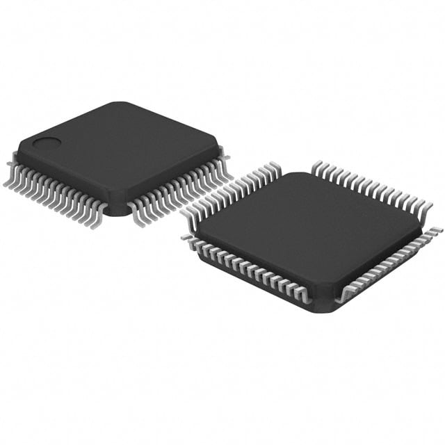
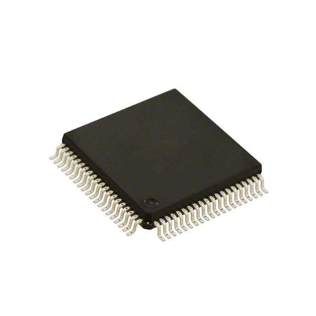
| 描述 | IC MCU 8BIT 128KB FLASH 64LQFP8位微控制器 -MCU 8BIT 128K FLASH |
| EEPROM容量 | - |
| 产品分类 | |
| I/O数 | 33 |
| 品牌 | Freescale Semiconductor |
| 产品手册 | |
| 产品图片 |
|
| rohs | 符合RoHS无铅 / 符合限制有害物质指令(RoHS)规范要求 |
| 产品系列 | 嵌入式处理器和控制器,微控制器 - MCU,8位微控制器 -MCU,Freescale Semiconductor MC9S08MM128CLHS08 |
| 数据手册 | |
| 产品型号 | MC9S08MM128CLH |
| RAM容量 | 12K x 8 |
| 产品种类 | 8位微控制器 -MCU |
| 供应商器件封装 | 64-LQFP(10x10) |
| 包装 | 托盘 |
| 单位重量 | 346.550 mg |
| 可用A/D通道 | 6 |
| 商标 | Freescale Semiconductor |
| 处理器系列 | MC9S08 |
| 外设 | LVD,POR,PWM,WDT |
| 封装 | Tray |
| 封装/外壳 | 64-LQFP |
| 工作温度 | -40°C ~ 85°C |
| 工作电源电压 | 1.8 V to 3.6 V |
| 工厂包装数量 | 800 |
| 振荡器类型 | 内部 |
| 数据RAM大小 | 12 kB |
| 数据Ram类型 | RAM |
| 数据总线宽度 | 8 bit |
| 数据转换器 | A/D 6x16b,D/A 1x12b |
| 最大工作温度 | + 105 C |
| 最大时钟频率 | 48 MHz |
| 最小工作温度 | - 40 C |
| 标准包装 | 800 |
| 核心 | S08 |
| 核心处理器 | S08 |
| 核心尺寸 | 8-位 |
| 片上ADC | Yes |
| 电压-电源(Vcc/Vdd) | 1.8 V ~ 3.6 V |
| 程序存储器大小 | 128 kB |
| 程序存储器类型 | Flash |
| 程序存储容量 | 128KB(128K x 8) |
| 系列 | S08MM |
| 连接性 | I²C, SCI, SPI, USB |
| 速度 | 48MHz |


- 商务部:美国ITC正式对集成电路等产品启动337调查
- 曝三星4nm工艺存在良率问题 高通将骁龙8 Gen1或转产台积电
- 太阳诱电将投资9.5亿元在常州建新厂生产MLCC 预计2023年完工
- 英特尔发布欧洲新工厂建设计划 深化IDM 2.0 战略
- 台积电先进制程称霸业界 有大客户加持明年业绩稳了
- 达到5530亿美元!SIA预计今年全球半导体销售额将创下新高
- 英特尔拟将自动驾驶子公司Mobileye上市 估值或超500亿美元
- 三星加码芯片和SET,合并消费电子和移动部门,撤换高东真等 CEO
- 三星电子宣布重大人事变动 还合并消费电子和移动部门
- 海关总署:前11个月进口集成电路产品价值2.52万亿元 增长14.8%


PDF Datasheet 数据手册内容提取
Freescale Semiconductor Document Number: MC9S08MM128 Data Sheet: Technical Data Rev. 3, 10/2010 An Energy-Efficient Solution from Freescale MC9S08MM128 series Covers: MC9S08MM128, and MC9S08MM64, MC9S08MM32, and MC9S08MM32A 64-LQFP 10mm x 10mm 80-LQFP 12mm x 12mm 81-MapBGA 10mm x10mm byte-by-byte data transfer; supports broadcast mode and 11-bit 8-Bit HCS08 Central Processor Unit (CPU) addressing – Up to 48-MHz CPU above 2.4V, 40MHz CPU above 2.1V, and – PRACMP — Analog comparator with selectable interrupt; 20MHz CPU above 1.8V across temperature of -40°C to 105°C compare option to programmable internal reference voltage; – HCS08 instruction set with added BGND instruction operation in stop3 – Support for up to 33 interrupt/reset sources – SCI — Two serial communications interfaces with optional 13-bit On-Chip Memory break; option to connect Rx input to PRACMP output on SCI1 and – 128K Dual Array Flash read/program/erase over full operating SCI2; High current drive on Tx on SCI1 and SCI2; wake-up from voltage and temperature stop3 on Rx edge – 12KB Random-access memory (RAM) – SPI1— Serial peripheral interface (SPI) with 64-bit FIFO buffer; – Security circuitry to prevent unauthorized access to RAM and 16-bit or 8-bit data transfers; full-duplex or single-wire Flash bidirectional; double-buffered transmit and receive; master or Power-Saving Modes slave mode; MSB-first or LSB-first shifting – Two ultra-low power stop modes. Peripheral clock enable register – SPI2— Serial peripheral interface with full-duplex or single-wire can disable clocks to unused modules to reduce currents bidirectional; Double-buffered transmit and receive; Master or – Time of Day (TOD) — Ultra-low power 1/4 sec counter with up to Slave mode; MSB-first or LSB-first shifting 64s timeout. – TPM — Two 4-channel Timer/PWM Module; Selectable input – Ultra-low power external oscillator that can be used in stop modes capture, output compare, or buffered edge- or center-aligned to provide accurate clock source to the TOD. 6 usec typical wake PWM on each channel; external clock input/pulse accumulator up time from stop3 mode – USB — Supports USB in full-speed device configuration. On-chip Clock Source Options transceiver and 3.3V regulator help save system cost, fully – Oscillator (XOSC1) — Loop-control Pierce oscillator; 32.768kHz compliant with USB Specification 2.0. Allows control, bulk, crystal or ceramic resonator dedicated for TOD operation. interrupt and isochronous transfers. Not available on – Oscillator (XOSC2) — for high frequency crystal input for MCG MC9S08MM32A devices. reference to be used for system clock and USB operations. – ADC16 — 16-bit Successive approximation ADC with up to 4 – Multipurpose Clock Generator (MCG) — PLL and FLL; precision dedicated differential channels and 8 single-ended channels; trimming of internal reference allows 0.2% resolution and 2% range compare function; 1.7mV/C temperature sensor; internal deviation over temperature and voltage; supports CPU bandgap reference channel; operation in stop3; fully functional frequencies from 4kHz to 48 MHz. from 3.6V to 1.8V, Configurable hardware trigger for 8 Channel System Protection select and result registers – Watchdog computer operating properly (COP) reset Watchdog – PDB — Programmable delay block with 16-bit counter and computer operating properly (COP) reset with option to run from modulus and prescale to set reference clock to bus divided by 1 to dedicated 1-kHz internal clock source or bus clock bus divided by 2048; 8 trigger outputs for ADC16 module provides – Low-voltage detection with reset or interrupt; selectable trip points; periodic coordination of ADC sampling sequence with sequence separate low-voltage warning with optional interrupt; selectable completion interrupt; Back-to-Back mode and Timed mode trip points – DAC— 12-bit resolution; 16-word data buffers with configurable – Illegal opcode and illegal address detection with reset watermark. – Flash block protection for each array to prevent accidental – OPAMP — Two flexible operational amplifiers configurable for write/erasure general operations; Low offset and temperature drift. – Hardware CRC to support fast cyclic redundancy checks – TRIAMP — Two trans-impedance amplifiers dedicated for Development Support converting current inputs into voltages. – Single-wire background debug interface Input/Output – Real-time debug with 6 hardware breakpoints (4 PC, 1 address – Up to 47 GPIOs and 2 output-only pin and 1 input-only pin. and 1 data) Breakpoint capability to allow single breakpoint setting – Voltage Reference output (VREFO). during in-circuit debugging – Dedicated infrared output pin (IRO) with – On-chip in-circuit emulator (ICE) debug module containing 3 high current sink capability. comparators and 9 trigger modes – Up to 16 KBI pins with selectable polarity. Peripherals Package Options – CMT— Carrier Modulator timer for remote control – 81-MBGA 10x10 mm communications. Carrier generator, modulator and driver for – 80-LQFP 12x12 mm dedicated infrared out. Can be used as an output compare timer. – 64-LQFP 10x10 mm – IIC— Up to 100 kbps with maximum bus loading; Multi-master operation; Programmable slave address; Interrupt driven Freescale reserves the right to change the detail specifications as may be required to permit improvements in the design of its products. ©Freescale Semiconductor, Inc., 2009-2010. All rights reserved. Freescale reserves the right to change the detail specifications as may be required to permit improvements in the design of its products.
Contents 1Devices in the MC9S08MM128 series. . . . . . . . . . . . . . . . . . . . .3 2.10 MCG and External Oscillator (XOSC) Characteristics .33 1.1 Pin Assignments. . . . . . . . . . . . . . . . . . . . . . . . . . . . . . .6 2.11 AC Characteristics . . . . . . . . . . . . . . . . . . . . . . . . . . . .36 1.1.1 64-Pin LQFP . . . . . . . . . . . . . . . . . . . . . . . . . . . .6 2.11.1Control Timing. . . . . . . . . . . . . . . . . . . . . . . . . .36 1.1.2 80-Pin LQFP . . . . . . . . . . . . . . . . . . . . . . . . . . . .8 2.11.2TPM Timing. . . . . . . . . . . . . . . . . . . . . . . . . . . .38 1.1.3 81-Pin MAPBGA . . . . . . . . . . . . . . . . . . . . . . . . .9 2.12 SPI Characteristics . . . . . . . . . . . . . . . . . . . . . . . . . . . .39 1.2 Pin Assignments by Packages . . . . . . . . . . . . . . . . . . .10 2.13 Flash Specifications . . . . . . . . . . . . . . . . . . . . . . . . . . .42 2.14 USB Electricals. . . . . . . . . . . . . . . . . . . . . . . . . . . . . . .43 2Electrical Characteristics. . . . . . . . . . . . . . . . . . . . . . . . . . . . . .13 2.15 VREF Electrical Specifications . . . . . . . . . . . . . . . . . . .44 2.1 Parameter Classification. . . . . . . . . . . . . . . . . . . . . . . .13 2.16 TRIAMP Electrical Parameters . . . . . . . . . . . . . . . . . . .46 2.2 Absolute Maximum Ratings . . . . . . . . . . . . . . . . . . . . .14 2.17 OPAMP Electrical Parameters. . . . . . . . . . . . . . . . . . . .47 2.3 Thermal Characteristics . . . . . . . . . . . . . . . . . . . . . . . .15 2.4 ESD Protection Characteristics . . . . . . . . . . . . . . . . . .16 3Ordering Information . . . . . . . . . . . . . . . . . . . . . . . . . . . . . . . . .48 2.5 DC Characteristics . . . . . . . . . . . . . . . . . . . . . . . . . . . .17 3.1 Device Numbering System . . . . . . . . . . . . . . . . . . . . . .48 2.6 Supply Current Characteristics. . . . . . . . . . . . . . . . . . .20 3.2 Package Information. . . . . . . . . . . . . . . . . . . . . . . . . . .49 2.7 PRACMP Electricals. . . . . . . . . . . . . . . . . . . . . . . . . . .23 3.3 Mechanical Drawings . . . . . . . . . . . . . . . . . . . . . . . . . .49 2.8 12-Bit DAC Electricals. . . . . . . . . . . . . . . . . . . . . . . . . .24 2.9 ADC Characteristics. . . . . . . . . . . . . . . . . . . . . . . . . . .26 4Revision History. . . . . . . . . . . . . . . . . . . . . . . . . . . . . . . . . . . . .49 Related Documentation Find the most current versions of all documents at: http://www.freescale.com. Reference Manual —MC9S08MM128RM Contains extensive product information including modes of operation, memory, resets and interrupts, register definition, port pins, CPU, and all module information. – 2 Freescale Semiconductor Freescale reserves the right to change the detail specifications as may be required to permit improvements in the design of its products.
Devices in the MC9S08MM128 series 1 Devices in the MC9S08MM128 series The following table summarizes the feature set available in the MC9S08MM128 series of MCUs. Table1. MC9S08MM128 series Features by MCU and Package Feature MC9S08MM128 MC9S08MM64 MC9S08MM32 MC9S08MM32A Pin quantity 81 80 64 64 64 64 FLASH size (bytes) 131072 65535 32768 32768 RAM size (bytes) 12K 12K 4K 2K Programmable Analog Comparator (PRACMP) yes yes yes yes Debug Module (DBG) yes yes yes yes Multipurpose Clock Generator (MCG) yes yes yes yes Inter-Integrated Communication (IIC) yes yes yes yes Interrupt Request Pin (IRQ) yes yes yes yes Keyboard Interrupt (KBI) 16 16 6 6 6 6 Port I/O1 47 46 33 33 33 33 Dedicated Analog Input Pins 12 12 12 12 Power and Ground Pins 8 8 8 8 Time Of Day (TOD) yes yes yes yes Serial Communications (SCI1) yes yes yes yes Serial Communications (SCI2) yes yes yes yes Serial Peripheral Interface 1 (SPI1 (FIFO)) yes yes yes yes Serial Peripheral Interface 2 (SPI2) yes yes yes yes Carrier Modulator Timer pin (IRO) yes yes yes yes TPM input clock pin (TPMCLK) yes yes yes yes TPM1 channels 4 4 4 4 TPM2 channels 4 4 2 2 2 2 XOSC1 yes yes yes yes XOSC2 yes yes yes yes USB yes yes yes no Programmable Delay Block (PDB) yes yes yes yes SAR ADC differential channels2 4 4 3 3 3 3 SAR ADC single-ended channels 8 8 6 6 6 6 DAC ouput pin (DACO) yes yes yes yes Voltage reference output pin (VREFO) yes yes yes yes General Purpose OPAMP (OPAMP) yes yes yes yes Trans-Impedance Amplifier (TRIAMP) yes yes yes yes 1 Port I/O count does not include two (2) output-only and one (1) input-only pins. 2 Each differential channel is comprised of 2 pin inputs. Freescale Semiconductor 3 Freescale reserves the right to change the detail specifications as may be required to permit improvements in the design of its products.
Devices in the MC9S08MM128 series A complete description of the modules included on each device is provided in the following table. Table2. Versions of On-Chip Modules Module Version Analog-to-Digital Converter (ADC16) 1 General Purpose Operational Amplifier (OPAMP) 1 Trans-Impedance Operational Amplifier (TRIAMP) 1 Digital to Analog Converter (DAC) 1 Programmable Delay Block 1 Inter-Integrated Circuit (IIC) 3 Central Processing Unit (CPU) 5 On-Chip In-Circuit Debug/Emulator (DBG) 3 Multi-Purpose Clock Generator (MCG) 3 Low Power Oscillator (XOSCVLP) 1 Carrier Modulator Timer (CMT) 1 Programable Analog Comparator (PRACMP) 1 Serial Communications Interface (SCI) 4 Serial Peripheral Interface (SPI) 5 Time of Day (TOD) 1 Universal Serial Bus (USB)1 1 Timer Pulse-Width Modulator (TPM) 3 System Integration Module (SIM) 1 Cyclic Redundancy Check (CRC) 3 Keyboard Interrupt (KBI) 2 Voltage Reference (VREF) 1 Voltage Regulator (VREG) 1 Interrupt Request (IRQ) 3 Flash Wrapper 1 GPIO 2 Port Control 1 1 USB Module not available on MC9S08MM32A devices. The block diagram in Figure1 shows the structure of the MC9S08MM128 series MCU. 4 Freescale Semiconductor Freescale reserves the right to change the detail specifications as may be required to permit improvements in the design of its products.
Devices in the MC9S08MM128 series Figure1. MC9S08MM128 series Block Diagram Freescale Semiconductor 5 Freescale reserves the right to change the detail specifications as may be required to permit improvements in the design of its products.
Devices in the MC9S08MM128 series 1.1 Pin Assignments This section shows the pin assignments for the MC9S08MM128 series devices. 1.1.1 64-Pin LQFP The following two figures show the 64-pin LQFP pinout configuration. The first illustrates the pinout configuration for MC9S08MM128, MC9S08MM64, and MC9S08MM32 devices. Q R K/I G0/SPSCK1F7/MISO1F6/MOSI1D1S1USB_DPB_DMSB33F2/TX2/TPM2CH0F1/RX2/TPM2CH1E6/RX2E5/TX2D3S3E4/CMPP3/TPMCL TTTDSBSSUTTTTDST PPPVVVUUVPPPPVVP 4321098765432109 PTA0/SS1 1666665555555555448 PTD7/RX1 IRO 2 47 PTD6/TX1 PTA4/INP1+ 3 46 PTD5/SCL/TPM1CH3 PTA5 4 45 PTD4/SDA/TPM1CH2 PTA6 5 44 PTD3/TPM1CH1 PTA7/INP2+ 6 43 PTD2/TPM1CH0 PTB0 7 42 PTD1/CMPP2/RESET PTB1/BLMS 8 64-LQFP 41 PTD0/BKGD/MS VSSA 9 40 PTC7/KBI2P2/CLKOUT/ADP11 VREFL 10 39 PTC6/KBI2P1/PRACMPO/ADP10 INP1- 11 38 PTC5/KBI2P0/CMPP1/ADP9 OUT1- 12 37 PTC4/KBI1P7/CMPP0/ADP8 13 36 PTC3/KBI1P6/SS2/ADP7 TRIOUT1/DADP2 VINP1 14 35 PTC2/KBI1P5/SPSCK2/ADP6 15 34 PTC1/MISO2 VINN1/DADM2 INP2- 16 33 PTC0/MOSI2 7890123456789012 1112222222222333 OUT2- DACORIOUT2/DADP3VINP2 VINN2/DADM3DADP0 DADM0VREFO VREFHVDDA VSS2PTB2/EXTAL1PTB3/XTAL1VDD2PTB4/EXTAL2PTB5/XTAL2 T Figure2. 64-Pin LQFP for MC9S08MM128, MC9S08MM64, and MC9S08MM32 devices For MC9S08MM32A devices, pins 56, 57, 58, and 59 are no connects (NC) as illustrated in the following figure. 6 Freescale Semiconductor Freescale reserves the right to change the detail specifications as may be required to permit improvements in the design of its products.
Devices in the MC9S08MM128 series Q R K/I SPSCK1MISO1MOSI1 TX2/TPM2CH0RX2/TPM2CH1RX2TX2 CMPP3/TPMCL G0/F7/F6/D1S1 F2/F1/E6/E5/D3S3E4/ TTTDSCCCCTTTTDST PPPVVNNNNPPPPVVP 4321098765432109 PTA0/SS1 1666665555555555448 PTD7/RX1 IRO 2 47 PTD6/TX1 PTA4/INP1+ 3 46 PTD5/SCL/TPM1CH3 PTA5 4 45 PTD4/SDA/TPM1CH2 PTA6 5 44 PTD3/TPM1CH1 PTA7/INP2+ 6 43 PTD2/TPM1CH0 PTB0 7 42 PTD1/CMPP2/RESET PTB1/BLMS 8 64-LQFP 41 PTD0/BKGD/MS VSSA 9 40 PTC7/KBI2P2/CLKOUT/ADP11 VREFL 10 39 PTC6/KBI2P1/PRACMPO/ADP10 INP1- 11 38 PTC5/KBI2P0/CMPP1/ADP9 OUT1- 12 37 PTC4/KBI1P7/CMPP0/ADP8 13 36 PTC3/KBI1P6/SS2/ADP7 TRIOUT1/DADP2 VINP1 14 35 PTC2/KBI1P5/SPSCK2/ADP6 15 34 PTC1/MISO2 VINN1/DADM2 INP2- 16 33 PTC0/MOSI2 7890123456789012 1112222222222333 OUT2- DACORIOUT2/DADP3VINP2 VINN2/DADM3DADP0 DADM0VREFO VREFHVDDA VSS2PTB2/EXTAL1PTB3/XTAL1VDD2PTB4/EXTAL2PTB5/XTAL2 T Figure3. 64-Pin LQFP for MC9S08MM32A devices Freescale Semiconductor 7 Freescale reserves the right to change the detail specifications as may be required to permit improvements in the design of its products.
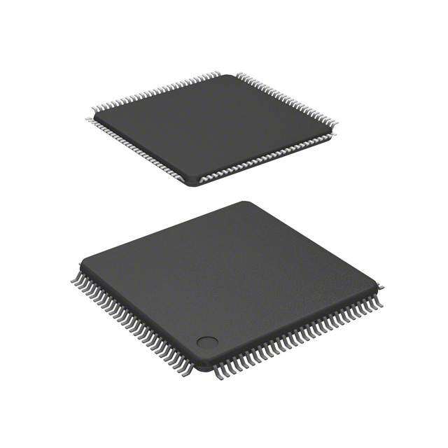
Devices in the MC9S08MM128 series 1.1.2 80-Pin LQFP The following figure shows the 80-pin LQFP pinout configuration. 01 HH CC 1 M2M2H2H3 G0/SPSCKF7/MISO1F6/MOSI1D1S1USB_DPB_DMSB33F5/KBI2P7F4/SDAF3/SCLF2/TX2/TPF1/RX2/TPF0/TPM2CE7/TPM2CE6/RX2E5/TX2D3S3 TTTDSBSSUTTTTTTTTTDS PPPVVVUUVPPPPPPPPPVV 09876543210987654321 PTA0/SS1 18777777777766666666660 PTE4/CMPP3/TPMCLK/IRQ IRO 2 59 PTE3/KBI2P6 PTA1/KBI1P0/TX1 3 58 PTE2/KBI2P5 PTA2/KBI1P1/RX1/ADP4 4 57 PTE1/KBI2P4 PTA3/KBI1P2/ADP5 5 56 PTE0/KBI2P3 PTA4/INP1+ 6 55 PTD7/RX1 PTA5 7 54 PTD6/TX1 PTA6 8 53 PTD5/SCL/TPM1CH3 PTA7/INP2+ 9 52 PTD4/SDA/TPM1CH2 PTB0 10 80-LQFP 51 PTD3/TPM1CH1 PTB1/BLMS 11 50 PTD2/TPM1CH0 VSSA 12 49 PTD1/CMPP2/RESET VREFL 13 48 PTD0/BKGD/MS INP1- 14 47 PTC7/KBI2P2/CLKOUT/ADP11 OUT1- 15 46 PTC6/KBI2P1/PRACMPO/ADP10 TRIOUT1/DADP2 16 45 PTC5/KBI2P0/CMPP1/ADP9 VINP1 17 44 PTC4/KBI1P7/CMPP0/ADP8 VINN1/DADM2 18 43 PTC3/KBI1P6/SS2/ADP7 INP2- 19 42 PTC2/KBI1P5/SPSCK2/ADP6 OUT2- 20 41 PTC1/MISO2 12345678901234567890 22222222233333333334 O 32 30 0O 1 1HA211222342 DAC RIOUT2/DADPVINP VINN2/DADMDADP DADMVREF DADP DADMVREFVDDVSSPTB2/EXTALPTB3/XTALVDDPTB4/EXTALPTB5/XTALPTB6/KBI1PPTB7/KBI1PPTC0/MOSI T Figure4. 80-Pin LQFP 8 Freescale Semiconductor Freescale reserves the right to change the detail specifications as may be required to permit improvements in the design of its products.
Devices in the MC9S08MM128 series 1.1.3 81-Pin MAPBGA The following figure shows the 81-pin MAPBGA pinout configuration. 1 2 3 4 5 6 7 8 9 A IRO PTG0 PTF6 USB_DP VBUS VUSB33 PTF4 PTF3 PTE4 B PTF7 PTA0 PTG1 USB_DM PTF5 PTE7 PTF1 PTF0 PTE3 C PTA4 PTA5 PTA6 PTA1 PTF2 PTE6 PTE5 PTE2 PTE1 D INP1- PTA7 PTB0 PTB1 PTA2 PTA3 PTD5 PTD7 PTE0 E OUT1 VINN1 OUT2 VDD2 VDD3 VDD1 PTD2 PTD3 PTD6 F VINP1 TRIOUT1 INP2- VSS2 VSS3 VSS1 PTB7 PTC7 PTD4 G DADP0 DACO TRIOUT2 VINN2 VREFO PTB6 PTC0 PTC1 PTC2 H DADM0 DADM1 DADP1 VINP2 PTC3 PTC4 PTD0 PTC5 PTC6 J VSSA VREFL VREFH VDDA PTB2 PTB3 PTD1 PTB4 PTB5 Figure5. 81-Pin MAPBGA Freescale Semiconductor 9 Freescale reserves the right to change the detail specifications as may be required to permit improvements in the design of its products.
Devices in the MC9S08MM128 series 1.2 Pin Assignments by Packages Table3. Package Pin Assignments Package A G P P Default ALT1 ALT2 ALT3 Composite Pin Name B F F Function P Q Q A L L M 0 4 1 8 6 8 B2 1 1 PTA0 SS1 — — PTA0/SS1 A1 2 2 IRO — — — IRO C4 3 — PTA1 KBI1P0 TX1 — PTA1/KBI1P0/TX1 D5 4 — PTA2 KBI1P1 RX1 ADP4 PTA2/KBI1P1/RX1/ADP4 D6 5 — PTA3 KBI1P2 ADP5 — PTA3/KBI1P2/ADP5 C1 6 3 PTA4 INP1+ — — PTA4/INP1+ C2 7 4 PTA5 — — — PTA5 C3 8 5 PTA6 — — — PTA6 D2 9 6 PTA7 INP2+ — — PTA7/INP2+ D3 10 7 PTB0 — — — PTB0 D4 11 8 PTB1 BLMS — — PTB1/BLMS J1 12 9 VSSA — — — VSSA J2 13 10 VREFL — — — VREFL D1 14 11 INP1- — — — INP1- E1 15 12 OUT1 — — — OUT1 F2 16 13 DADP2 TRIOUT1 — — DADP2/TRIOUT1 F1 17 14 VINP1 — — — VINP1 E2 18 15 DADM2 VINN1 — — DADM2/VINN1 F3 19 16 INP2- — — — INP2- E3 20 17 OUT2 — — — OUT2 G2 21 18 DACO — — — DACO G3 22 19 DADP3 TRIOUT2 — — DADP3/TRIOUT2 H4 23 20 VINP2 — — — VINP2 G4 24 21 DADM3 VINN2 — — DADM3/VINN2 G1 25 22 DADP0 — — — DADP0 H1 26 23 DADM0 — — — DADM0 G5 27 24 VREFO — — — VREFO H3 28 — DADP1 — — — DADP1 H2 29 — DADM1 — — — DADM1 10 Freescale Semiconductor Freescale reserves the right to change the detail specifications as may be required to permit improvements in the design of its products.
Devices in the MC9S08MM128 series Table3. Package Pin Assignments (Continued) Package A G P P Default ALT1 ALT2 ALT3 Composite Pin Name B F F Function P Q Q A L L M 0 4 1 8 6 8 J3 30 25 VREFH — — — VREFH J4 31 26 VDDA — — — VDDA F4 32 27 VSS2 — — — VSS2 J5 33 28 PTB2 EXTAL1 — — PTB2/EXTAL1 J6 34 29 PTB3 XTAL1 — — PTB3/XTAL1 E4 35 30 VDD2 — — — VDD2 J8 36 31 PTB4 EXTAL2 — — PTB4/EXTAL2 J9 37 32 PTB5 XTAL2 — — PTB5/XTAL2 G6 38 — PTB6 KBI1P3 — — PTB6/KBI1P3 F7 39 — PTB7 KBI1P4 — — PTB7/KBI1P4 G7 40 33 PTC0 MOSI2 — — PTC0/MOSI2 G8 41 34 PTC1 MISO2 — — PTC1/MISO2 G9 42 35 PTC2 KBI1P5 SPSCK2 ADP6 PTC2/KBI1P5/SPSCK2/ADP6 H5 43 36 PTC3 KBI1P6 SS2 ADP7 PTC3/KBI1P6/SS2/ADP7 H6 44 37 PTC4 KBI1P7 CMPP0 ADP8 PTC4/KBI1P7/CMPP0/ADP8 H8 45 38 PTC5 KBI2P0 CMPP1 ADP9 PTC5/KBI2P0/CMPP1/ADP9 H9 46 39 PTC6 KBI2P1 PRACMPO ADP10 PTC6/KBI2P1/PRACMPO/ADP10 F8 47 40 PTC7 KBI2P2 CLKOUT ADP11 PTC7/KBI2P2/CLKOUT/ADP11 H7 48 41 PTD0 BKGD MS — PTD0/BKGD/MS J7 49 42 PTD1 CMPP2 RESET — PTD1/CMPP2/RESET E7 50 43 PTD2 TPM1CH0 — — PTD2TPM1CH0 E8 51 44 PTD3 TPM1CH1 — — PTD3/TPM1CH1 F9 52 45 PTD4 SDA TPM1CH2 — PTD4/SDA/TPM1CH2 D7 53 46 PTD5 SCL TPM1CH3 — PTD5/SCL/TPM1CH3 E9 54 47 PTD6 TX1 — — PTD6/TX1 D8 55 48 PTD7 RX1 — — PTD7/RX1 D9 56 — PTE0 KBI2P3 — — PTE0/KBI2P3 C9 57 — PTE1 KBI2P4 — — PTE1/KBI2P4 C8 58 — PTE2 KBI2P5 — — PTE2/KBI2P5 B9 59 — PTE3 KBI2P6 — — PTE3/KBI2P6 A9 60 49 PTE4 CMPP3 TPMCLK IRQ PTE4/CMPP3/TPMCLK/IRQ Freescale Semiconductor 11 Freescale reserves the right to change the detail specifications as may be required to permit improvements in the design of its products.
Devices in the MC9S08MM128 series Table3. Package Pin Assignments (Continued) Package A G P P Default ALT1 ALT2 ALT3 Composite Pin Name B F F Function P Q Q A L L M 0 4 1 8 6 8 F5 61 50 VSS3 — — — VSS3 E5 62 51 VDD3 — — — VDD3 C7 63 52 PTE5 TX2 — — PTE5/TX2 C6 64 53 PTE6 RX2 — — PTE6/RX2 B6 65 — PTE7 TPM2CH3 — — PTE7/TPM2CH3 B8 66 — PTF0 TPM2CH2 — — PTF0/TPM2CH2 B7 67 54 PTF1 RX2 TPM2CH1 — PTF1/RX2/TPM2CH1 C5 68 55 PTF2 TX2 TPM2CH0 — PTF2/TX2/TPM2CH0 A8 69 — PTF3 SCL — — PTF3/SCL A7 70 — PTF4 SDA — — PTF4/SDA B5 71 — PTF5 KBI2P7 — — PTF5/KBI2P7 A6 72 56 VUSB331 — — — VUSB33 B4 73 57 USB_DM2 — — — USB_DM A4 74 58 USB_DP3 — — — USB_DP A5 75 59 VBUS4 — — — VBUS F6 76 60 VSS1 — — — VSS1 E6 77 61 VDD1 — — — VDD1 A3 78 62 PTF6 MOSI1 — — PTF6/MOSI1 B1 79 63 PTF7 MISO1 — — PTF7/MISO1 A2 80 64 PTG0 SPSCK1 — — PTG0/SPSCK1 B3 — — PTG1 — — — PTG1 1 NC on MC9S08MM32A devices. 2 NC on MC9S08MM32A devices. 3 NC on MC9S08MM32A devices. 4 NC on MC9S08MM32A devices. 12 Freescale Semiconductor Freescale reserves the right to change the detail specifications as may be required to permit improvements in the design of its products.
Electrical Characteristics 2 Electrical Characteristics This section contains electrical specification tables and reference timing diagrams for the MC9S08MM128/64/32/32A microcontroller, including detailed information on power considerations, DC/AC electrical characteristics, and AC timing specifications. The electrical specifications are preliminary and are from previous designs or design simulations. These specifications may not be fully tested or guaranteed at this early stage of the product life cycle. These specifications will, however, be met for production silicon. Finalized specifications will be published after complete characterization and device qualifications have been completed. NOTE The parameters specified in this data sheet supersede any values found in the module specifications. 2.1 Parameter Classification The electrical parameters shown in this supplement are guaranteed by various methods. To give the customer a better understanding, the following classification is used and the parameters are tagged accordingly in the tables where appropriate: Table4. Parameter Classifications P Those parameters are guaranteed during production testing on each individual device. Those parameters are achieved by the design characterization by measuring a statistically relevant C sample size across process variations. Those parameters are achieved by design characterization on a small sample size from typical devices T under typical conditions unless otherwise noted. All values shown in the typical column are within this category. D Those parameters are derived mainly from simulations. NOTE The classification is shown in the column labeled “C” in the parameter tables where appropriate. Freescale Semiconductor 13 Freescale reserves the right to change the detail specifications as may be required to permit improvements in the design of its products.
Electrical Characteristics 2.2 Absolute Maximum Ratings Absolute maximum ratings are stress ratings only, and functional operation at the maxima is not guaranteed. Stress beyond the limits specified in the following table may affect device reliability or cause permanent damage to the device. For functional operating conditions, refer to the remaining tables in this section. Table5. Absolute Maximum Ratings # Rating Symbol Value Unit 1 Supply voltage V –0.3 to +3.8 V DD 2 Maximum current into V I 120 mA DD DD 3 Digital input voltage V –0.3 to V +0.3 V In DD Instantaneous maximum current I 25 mA 4 D Single pin limit (applies to all port pins)1,2,3 5 Storage temperature range T –55 to 150 C stg 1 Input must be current limited to the value specified. To determine the value of the required current-limiting resistor, calculate resistance values for positive (V ) and negative (V ) clamp DD SS voltages, then use the larger of the two resistance values. 2 All functional non-supply pins are internally clamped to V and V . SS DD 3 Power supply must maintain regulation within operating V range during instantaneous and operating DD maximum current conditions. If positive injection current (V > V ) is greater than I , the injection In DD DD current may flow out of V and could result in external power supply going out of regulation. Ensure DD external V load will shunt current greater than maximum injection current. This will be the greatest DD risk when the MCU is not consuming power. Examples are: if no system clock is present, or if the clock rate is very low (which would reduce overall power consumption). This device contains circuitry protecting against damage due to high static voltage or electrical fields; however, it is advised that normal precautions be taken to avoid application of any voltages higher than maximum-rated voltages to this high-impedance circuit. Reliability of operation is enhanced if unused inputs are tied to an appropriate logic voltage level (for instance, either V or V ). SS DD 14 Freescale Semiconductor Freescale reserves the right to change the detail specifications as may be required to permit improvements in the design of its products.
Electrical Characteristics 2.3 Thermal Characteristics This section provides information about operating temperature range, power dissipation, and package thermal resistance. Power dissipation on I/O pins is usually small compared to the power dissipation in on-chip logic and it is user-determined rather than being controlled by the MCU design. In order to take P into account in power calculations, determine the difference between I/O actual pin voltage and V or V and multiply by the pin current for each I/O pin. Except in cases of unusually high pin current SS DD (heavy loads), the difference between pin voltage and V or V will be very small. SS DD Table6. Thermal Characteristics # Symbol Rating Value Unit 1 T Operating temperature range (packaged): C A MC9S08MM128 –40 to 105 MC9S08MM64 –40 to 105 MC9S08MM32 –40 to 105 MC9S08MM32A –40 to 105 2 T Maximum junction temperature 135 C JMAX 3 Thermal resistance1,2,3,4 Single-layer board — 1s C/W JA 81-pin MBGA 77 80-pin LQFP 55 64-pin LQFP 68 4 Thermal resistance1, 2, 3, 4 Four-layer board — 2s2p C/W JA 81-pin MBGA 47 80-pin LQFP 40 64-pin LQFP 49 1 Junction temperature is a function of die size, on-chip power dissipation, package thermal resistance, mounting site (board) temperature, ambient temperature, air flow, power dissipation of other components on the board, and board thermal resistance. 2 Junction to Ambient Natural Convection 3 1s — Single layer board, one signal layer 4 2s2p — Four layer board, 2 signal and 2 power layers The average chip-junction temperature (T ) in C can be obtained from: J T = T + (P ) Eqn.1 J A D JA where: T = Ambient temperature, C A = Package thermal resistance, junction-to-ambient, C/W JA P = P P D int I/O P = I V , Watts — chip internal power int DD DD P = Power dissipation on input and output pins — user determined I/O Freescale Semiconductor 15 Freescale reserves the right to change the detail specifications as may be required to permit improvements in the design of its products.
Electrical Characteristics For most applications, P P and can be neglected. An approximate relationship between P and T (if P is neglected) I/O int D J I/O is: P = K (T + 273C) Eqn.2 D J Solving Equation1 and Equation2 for K gives: K = P (T + 273C) + (P )2 Eqn.3 D A JA D where K is a constant pertaining to the particular part. K can be determined from Equation3 by measuring P (at equilibrium) D for a known T . Using this value of K, the values of P and T can be obtained by solving Equation1 and Equation2 iteratively A D J for any value of T . A 2.4 ESD Protection Characteristics Although damage from static discharge is much less common on these devices than on early CMOS circuits, normal handling precautions should be used to avoid exposure to static discharge. Qualification tests are performed to ensure that these devices can withstand exposure to reasonable levels of static without suffering any permanent damage. All ESD testing is in conformity with CDF-AEC-Q00 Stress Test Qualification for Automotive Grade Integrated Circuits. (http://www.aecouncil.com/) This device was qualified to AEC-Q100 Rev E. A device is considered to have failed if, after exposure to ESD pulses, the device no longer meets the device specification requirements. Complete dc parametric and functional testing is performed per the applicable device specification at room temperature followed by hot temperature, unless specified otherwise in the device specification. Table7. ESD and Latch-up Test Conditions Model Description Symbol Value Unit Human Body Series Resistance R1 1500 Storage Capacitance C 100 pF Number of Pulse per pin — 3 — Machine Series Resistance R1 0 Storage Capacitance C 200 pF Number of Pulse per pin — 3 — Latch-up Minimum input voltage limit — –2.5 V Maximum input voltage limit — 7.5 V Table8. ESD and Latch-Up Protection Characteristics # Rating Symbol Min Max Unit C 1 Human Body Model (HBM) V 2000 — V T HBM 2 Machine Model (MM) V 200 — V T MM 3 Charge Device Model (CDM) V 500 — V T CDM 4 Latch-up Current at T = 125C I 00 — mA T A LAT 16 Freescale Semiconductor Freescale reserves the right to change the detail specifications as may be required to permit improvements in the design of its products.
Electrical Characteristics 2.5 DC Characteristics This section includes information about power supply requirements, I/O pin characteristics, and power supply current in various operating modes. Table9. DC Characteristics Num Symbol Characteristic Condition Min Typ1 Max Unit C V Operating — 1.82 — 3.6 V 1 DD — Voltage V Output high All I/O pins, low-drive strength 2 OH voltage V 1.8 V, V – 0.5 — — V DD DD C I = –600 A Load All I/O pins, high-drive strength V 2.7 V, V – 0.5 — — V DD DD P I = –10 mA Load V 1.8V, V – 0.5 — — V DD DD C I = –3 mA Load I Output high Max total I for all ports 3 OHT OH current — — — 100 mA D V Output low All I/O pins, low-drive strength 4 OL voltage V 1.8 V, — — 0.5 V DD C I = 600 A Load All I/O pins, high-drive strength V 2.7 V, — — 0.5 V DD P I = 10 mA Load V 1.8 V, — — 0.5 V DD C I = 3 mA Load I Output low Max total I — — — 100 mA 5 OLT OL D current for all ports 6 V Input high voltage all digital inputs IH all digital inputs, 0.70 x V — — V DD P V 2.7 V DD all digital inputs, 0.85 x V — — V DD 2.7 V > V P DD 1.8 V Freescale Semiconductor 17 Freescale reserves the right to change the detail specifications as may be required to permit improvements in the design of its products.
Electrical Characteristics Table9. DC Characteristics (Continued) Num Symbol Characteristic Condition Min Typ1 Max Unit C 7 V Input low voltage all digital inputs IL all digital inputs, — — 0.35 x V P V 2.7 V V DD DD all digital inputs, — — 0.30 x V 2.7 V 1.8 V P DD DD V 8 V Input hysteresis all digital inputs — 0.06 x V — — mV C hys DD |I Input leakage all input only V = V or V — — 0.5 A In| In DD SS 9 current pins P (Per pin) |IOZ| Hi-Z (off-state) all digital VIn = VDD or VSS — 0.003 0.5 A 10 leakage current3 input/output P (per pin) 11 R Pull-up resistors — 17.5 — 52.5 k P PU R Internal 17.5 — 52.5 k PD 12 pull-down — P resistors4 I DC injection Single pin limit 13 IC current 5, 6, 7 V > V > V –0.2 — 0.2 mA D SS IN DD Total MCU limit, includes sum of allstressed pins V > V > V –5 — 5 mA D SS IN DD 14 C Input Capacitance, all pins — — — 8 pF C In 15 V RAM retention voltage — — 0.6 1.0 V C RAM 16 V POR re-arm voltage8 — 0.9 1.4 1.79 V C POR 17 t POR re-arm time — 10 — — s D POR V 9 Low-voltage V falling LVDH DD detection 18 threshold — high range — 2.11 2.16 2.22 V P V rising DD — 2.16 2.23 2.27 V P V Low-voltage V falling LVDL DD detection 19 threshold — low range9 — 1.80 1.84 1.88 V P V rising DD — 1.88 1.93 1.96 V P 18 Freescale Semiconductor Freescale reserves the right to change the detail specifications as may be required to permit improvements in the design of its products.
Electrical Characteristics Table9. DC Characteristics (Continued) Num Symbol Characteristic Condition Min Typ1 Max Unit C V Low-voltage V falling LVWH DD warning 20 threshold — high range9 — 2.36 2.46 2.56 V P V rising DD — 2.36 2.46 2.56 V P V Low-voltage V falling LVWL DD warning 21 threshold — low range9 — 2.11 2.16 2.22 V P V rising DD — 2.16 2.23 2.27 V P V Low-voltage inhibit reset/recover 22 hys — — 50 — mV C hysteresis10 23 V Bandgap Voltage Reference11 — 1.15 1.17 1.18 V P BG 1 Typical values are measured at 25C. Characterized, not tested 2 As the supply voltage rises, the LVD circuit will hold the MCU in reset until the supply has risen above V . LVDL 3 Does not include analog module pins. Dedicated analog pins should not be pulled to V or V and should be left DD SS floating when not used to reduce current leakage. 4 Measured with V = V . In DD 5 All functional non-supply pins are internally clamped to V and V except PTD1. SS DD 6 Input must be current limited to the value specified. To determine the value of the required current-limiting resistor, calculate resistance values for positive and negative clamp voltages, then use the larger of the two values. 7 Power supply must maintain regulation within operating V range during instantaneous and operating maximum DD current conditions. If positive injection current (V > V ) is greater than I , the injection current may flow out of V In DD DD DD and could result in external power supply going out of regulation. Ensure external V load will shunt current greater DD than maximum injection current. This will be the greatest risk when the MCU is not consuming power. Examples are: if no system clock is present, or if clock rate is very low (which would reduce overall power consumption). 8 Maximum is highest voltage that POR is guaranteed. 9 Run at 1 MHz bus frequency 10Low voltage detection and warning limits measured at 1 MHz bus frequency. 11Factory trimmed at V = 3.0 V, Temp = 25C DD Freescale Semiconductor 19 Freescale reserves the right to change the detail specifications as may be required to permit improvements in the design of its products.
Electrical Characteristics 2.6 Supply Current Characteristics Table10. Supply Current Characteristics Bus Temp # Symbol Parameter V (V) Typ1 Max Unit C Freq DD (C) RI Run supply FEI mode; all modules ON2 DD 1 current 3 –40 to 24 MHz 20 24 mA P 25 24 MHz 3 20 24 mA 105 P 3 –40 to 20 MHz 18 — mA T 105 3 –40 to 8 MHz 8 — mA T 105 3 –40 to 1 MHz 1.8 — mA T 105 RI Run supply FEI mode; all modules OFF3 2 DD current –40 to 24 MHz 3 12.3 14.1 mA C 105 –40 to 20 MHz 3 10.5 — mA T 105 3 –40 to 8 MHz 4.8 — mA T 105 3 –40 to 1 MHz 1.3 — mA T 105 RI Run supply LPS=0; all modules OFF3 3 DD current 16 kHz 3 –40 to 153 222 A T FBILP 105 16 kHz 3 –40 to 143 200 A T FBELP 105 4 RIDD Rcuurnre snutpply LPS=1, all modules OFF3 16 kHz 3 20 26 A 0 to 70 T FBELP 16 kHz 3 –40 to 20 70 A T FBELP 105 20 Freescale Semiconductor Freescale reserves the right to change the detail specifications as may be required to permit improvements in the design of its products.
Electrical Characteristics Table10. Supply Current Characteristics (Continued) Bus Temp # Symbol Parameter V (V) Typ1 Max Unit C Freq DD (C) 5 WIDD Wsuapipt lmy ocduerr ent FEI mode, all modules OFF3 3 –40 to 24 MHz 6.7 — mA C 105 3 –40 to 20 MHz 5.6 — mA T 105 3 –40 to 8 MHz 2.4 — mA T 105 3 –40 to 1 MHz 1 — mA T 105 Low-Power 6 LPWIDD Wait mode supply current 3 –40 to 16 KHz 10 40 µA T 105 Stop2 mode 7 S2IDD supply cur- rent4 3 –40 to N/A 0.39 0.8 µA P 25 N/A 3 2.4 4.5 µA 70 C N/A 3 7 11 µA 85 C N/A 3 16 22 µA 105 P 2 –40 to N/A 0.2 0.45 µA C 25 N/A 2 2 3.8 µA 70 C N/A 2 8 12 µA 85 C N/A 2 10 20 µA 105 C Freescale Semiconductor 21 Freescale reserves the right to change the detail specifications as may be required to permit improvements in the design of its products.
Electrical Characteristics Table10. Supply Current Characteristics (Continued) Bus Temp # Symbol Parameter V (V) Typ1 Max Unit C Freq DD (C) Stop3 mode No clocks active S3IDD supply current4 3 –40 to N/A 0.55 0.9 µA P 25 N/A 3 5.5 8.9 µA 70 C N/A 3 14 18 µA 85 C 8 N/A 3 37 42 µA 105 P 2 0.35 0.5 –40 to N/A µA C 25 N/A 2 3.8 6.8 µA 70 C N/A 2 14 20 µA 85 C N/A 2 25 46 µA 105 C 1 Data in Typical column was characterized at 3.0 V, 25°C or is typical recommended value. 2 ON = System Clock Gating Control registers turn on system clock to the corresponding modules. 3 OFF = System Clock Gating Control registers turn off system clock to the corresponding modules. 4 All digital pins must be configured to a known state to prevent floating pins from adding current. Smaller packages may have some pins that are not bonded out; however, software must still be configured to the largest pin package available so that all pins are in a known state. Otherwise, floating pins that are not bonded in the smaller packages may result in a higher current draw. NOTE: I/O pins are configured to output low, input-only pins are configured to pullup enabled. IRO pin connects to ground. TRIAMPx, OPAMPx, DACO, and VREFO pins are at reset state and unconnected. Table11. Typical Stop Mode Adders Temperature (°C) # Parameter Condition Units C –40 25 70 85 105 1 LPO — 50 75 100 150 250 nA D 2 EREFSTEN RANGE=HGO=0 600 650 750 850 1000 nA D 3 IREFSTEN1 — — 73 80 92 125 µA T TOD Does not include clock source 50 75 100 150 250 nA D 4 current PRACMP1 Not using the bandgap 30 35 40 55 75 µA T 5 (BGBE=0) ADC1 ADLPC=ADLSMP=1 190 195 210 220 260 µA T 6 Not using the bandgap (BGBE=0) 22 Freescale Semiconductor Freescale reserves the right to change the detail specifications as may be required to permit improvements in the design of its products.
Electrical Characteristics Table11. Typical Stop Mode Adders (Continued) Temperature (°C) # Parameter Condition Units C –40 25 70 85 105 DAC1 High-Power mode; no load on 369 377 377 390 410 µA T 7 DACO Low-Power mode 50 51 51 52 60 µA T OPAMP1 High-Power mode 453 538 538 540 540 µA T 8 Low-Power mode 56 67 67 68 70 µA T TRIAMP1 High-Power mode 430 432 433 438 478 µA T 9 Low-Power mode 52 52 52 55 60 µA T 1 Not available in stop2 mode. 2.7 PRACMP Electricals Table12. PRACMP Electrical Specifications # Characteristic Symbol Min Typical Max Unit C 1 Supply voltage V 1.8 — 3.6 V P PWR 2 Supply current (active) (PRG enabled) I — — 80 A D DDACT1 3 Supply current (active) (PRG disabled) I — — 40 A D DDACT2 Supply current (ACMP and PRG all I — — 2 nA D 4 DDDIS disabled) 5 Analog input voltage VAIN V – 0.3 — V V D SS DD 6 Analog input offset voltage VAIO — 5 40 mV D 7 Analog comparator hysteresis V 3.0 — 20.0 mV D H 8 Analog input leakage current I — — 1 nA D ALKG 9 Analog comparator initialization delay tAINIT — — 1.0 s D 10 Programmable reference generator inputs V (V ) 1.8 — 2.75 V D In2 DD25 Programmable reference generator setup t — 1 — µs D 11 PRGST delay Programmable reference generator step Vstep 0.75 1 1.25 LSB D 12 size Programmable reference generator voltage Vprgout V /32 — V V P 13 In in range Freescale Semiconductor 23 Freescale reserves the right to change the detail specifications as may be required to permit improvements in the design of its products.
Electrical Characteristics 2.8 12-Bit DAC Electricals Table13. DAC 12LV Operating Requirements # Characteristic Symbol Min Max Unit C Notes 1 Supply voltage V 1.8 3.6 V P DDA 2 Reference voltage V 1.15 3.6 V C DACR 3 Temperature T –40 105 °C C A Output load capacitance C A small load capacitance L (47 pF) can improve the 4 — 100 pF C bandwidth performance of the DAC. 5 Output load current I — 1 mA C L Table14. DAC 12-Bit Operating Behaviors # Characteristic Symbol Min Typ Max Unit C Notes 1 Resolution N 12 — 12 bit T Supply current low-power mode I µA 2 DDA_DACLP — 50 100 T 3 Supply current high-power mode I — 345 500 µA T DDA_DACHP Full-scale Settling time Ts LP (cid:129) V = 3V FS DDA (±1 LSB) or 2.2 V 4 (0x080 to 0xF7F or 0xF7F to — — 200 µs T (cid:129) VREFSEL = 1 0x080) (cid:129) Temperature = 25°C low-power mode Full-scale Settling time Ts HP (cid:129) V = 3V FS DDA (±1 LSB) or 2.2 V 5 (0x080 to 0xF7F or 0xF7F to — — 30 µs T (cid:129) VREFSEL = 1 0x080) (cid:129) Temperature = 25°C high-power mode Code-to-code Settling time Ts LP (cid:129) V = 3V C-C DDA (±1 LSB) or 2.2 V 6 (0xBF8 to 0xC08 or 0xC08 to — — 5 µs T (cid:129) VREFSEL = 1 0xBF8) (cid:129) Temperature = 25°C low-power mode Code-to-code Settling time Ts HP (cid:129) V = 3V C-C DDA (±1 LSB) or 2.2 V (0xBF8 to 0xC08 or 0xC08 to (cid:129) VREFSEL = 1 7 0xBF8) — 1 — µs T (cid:129) Temperature = 25°C high-power mode (3 V at Room Temperature) DAC output voltage range low V dacoutl (high-power mode, no load, DAC 8 — — 100 mV T set to 0) (3 V at Room Temperature) 24 Freescale Semiconductor Freescale reserves the right to change the detail specifications as may be required to permit improvements in the design of its products.
Electrical Characteristics Table14. DAC 12-Bit Operating Behaviors (Continued) # Characteristic Symbol Min Typ Max Unit C Notes DAC output voltage range high V dacouth V - 9 (high-power mode, no load, DAC DACR — — mV T 100 set to 0x0FFF) 10 Integral non-linearity error INL — — ± 8 LSB T Differential non-linearity error DNL 11 — — ± 1 LSB T VDACR is > 2.4 V Offset error E Calculated by a O best fit curve 12 — ±0.4 ± 3 %FSR T from V + SS 100mV to V –100mV REFH Gain error, V = V = V E Calculated by a REFH ext DD G best fit curve from V + 13 — ±0.1 ± 0.5 %FSR T SS 100mV to V –100mV REFH Power supply rejection ratio PSRR 14 60 — — dB T V 2.4 V DD Temperature drift of offset voltage T See Typical co 15 (DAC set to 0x0800) — — 2 mV T Drift figure that follows. 16 Offset aging coefficient A — — 8 µV/yr T c Figure6. Offset at Half Scale vs Temperature Freescale Semiconductor 25 Freescale reserves the right to change the detail specifications as may be required to permit improvements in the design of its products.
Electrical Characteristics 2.9 ADC Characteristics Table15. 16-Bit ADC Operating Conditions # Symb Characteristic Conditions Min Typ1 Max Unit C Comment 1 V Supply voltage Absolute 1.8 — 3.6 V D DDA V Delta to V –100 0 +100 2 DDA DD mV D (V –V )2 DD DDA V Ground voltage Delta to V –100 0 +100 3 SSA SS mV D (V –V )2 SS SSA 4 V Ref Voltage High 1.15 V V V D REFH DDA DDA 5 V Ref Voltage Low V V V V D REFL SSA SSA SSA 6 V Input Voltage V — V V D ADIN REFL REFH C Input 16-bit modes — 8 10 7 ADIN pF T Capacitance 8/10/12-bit modes 4 5 8 R Input Resistance — 2 5 k T ADIN R Analog Source External to AS Resistance MCU 9 Assumes ADLSMP=0 16-bit mode — — 0.5 k T f > 8 MHz ADCK 4 MHz < f < 8 — — 1 ADCK k T MHz f < 4 MHz — — 2 k T ADCK 13/12-bit mode — — 1 k T f > 8 MHz ADCK 4 MHz < f < 8 — — 2 ADCK k T MHz f < 4 MHz — — 5 k T ADCK 11/10-bit mode — — 2 k T f > 8 MHz ADCK 4 MHz < f < 8 — — 5 ADCK k T MHz f < 4 MHz — — 10 k T ADCK 9/8-bit mode — — 5 k T f > 8 MHz ADCK f < 8 MHz — — 10 k T ADCK 26 Freescale Semiconductor Freescale reserves the right to change the detail specifications as may be required to permit improvements in the design of its products.
Electrical Characteristics Table15. 16-Bit ADC Operating Conditions (Continued) # Symb Characteristic Conditions Min Typ1 Max Unit C Comment f ADC Conversion Clock 10 ADCK Frequency ADLPC=0, ADHSC=1 1.0 — 8.0 MHz D ADLPC=0, ADHSC=0 1.0 — 5.0 MHz D ADLPC=1, ADHSC=0 1.0 — 2.5 MHz D 1 Typical values assume V = 3.0 V, Temp = 25 C, f =1.0 MHz unless otherwise stated. Typical values are for DDA ADCK reference only and are not tested in production. 2 DC potential difference. SIMPLIFIED INPUT PIN EQUIVALENT CIRCUIT ZADIN SIMPLIFIED Pad ZAS leakage CHANNEL SELECT due to CIRCUIT ADC SAR R input R ENGINE AS protection ADIN + V ADIN – C V + AS AS – R ADIN INPUT PIN R ADIN INPUT PIN R ADIN INPUT PIN C ADIN Figure7. ADC Input Impedance Equivalency Diagram Freescale Semiconductor 27 Freescale reserves the right to change the detail specifications as may be required to permit improvements in the design of its products.
Electrical Characteristics Table16. 16-Bit SAR ADC Characteristics full operating range (V = V , > 1.8, V = V 8 MHz, –40 to 85 °C) REFH DDA REFL SSA # Characteristic Conditions1 Symb Min Typ2 Max Unit C Comment Supply Current ADLPC=1, ADHSC=0 — 215 — ADLSMP 1 ADLPC=0, ADHSC=0 I — 470 — A T =0 DDAD ADCO=1 ADLPC=0, ADHSC=1 — 610 — 2 Supply Current Stop, Reset, Module Off I — 0.01 — A T DDAD ADC ADLPC=1, ADHSC=0 — 2.4 — Asynchronous C 3 Clock Source ADLPC=0, ADHSC=0 f — 5.2 — MHz t = ADACK ADACK 1/f ADLPC=0, ADHSC=1 — 6.2 — ADACK 4 Sample Time See Reference Manual for sample times Conversion See Reference Manual for conversion times 5 Time Total 16-bit differential mode TUE — 16 48/ –40 LSB3 T 32x Unadjusted 16-bit single-ended mode — 20 56/ –28 Hardware Error Averaging 6 (AVGE = %1 AVGS = %11) 13-bit differential mode — 1.5 3.0 T 12-bit single-ended mode — 1.75 3.5 11-bit differential mode — 0.7 1.5 T 10-bit single-ended mode — 0.8 1.5 9-bit differential mode — 0.5 1.0 T 8-bit single-ended mode — 0.5 1.0 Differential 16-bit differential mode DNL — 2.5 5/–3 LSB2 T 7 Non-Linearity 16-bit single-ended mode — 2.5 +5/–3 13-bit differential mode — 0.7 1 T 12-bit single-ended mode — 0.7 1 11-bit differential mode — 0.5 0.75 T 10-bit single-ended mode — 0.5 0.75 9-bit differential mode — 0.2 0.5 T 8-bit single-ended mode — 0.2 0.5 28 Freescale Semiconductor Freescale reserves the right to change the detail specifications as may be required to permit improvements in the design of its products.
Electrical Characteristics Table16. 16-Bit SAR ADC Characteristics full operating range (V = V , > 1.8, V = V 8 MHz, –40 to 85 °C) (Continued) REFH DDA REFL SSA # Characteristic Conditions1 Symb Min Typ2 Max Unit C Comment Integral 16-bit differential mode INL — 6.0 16.0 LSB2 T 8 Non-Linearity 16-bit single-ended mode — 10.0 20.0 13-bit differential mode — 1.0 2.5 T 12-bit single-ended mode — 1.0 2.5 11-bit differential mode — 0.5 1.0 T 10-bit single-ended mode — 0.5 1.0 9-bit differential mode — 0.3 0.5 T 8-bit single-ended mode — 0.3 0.5 Zero-Scale 16-bit differential mode E — 4.0 +32/ –24 LSB2 T V = 9 ZS ADIN Error 16-bit single-ended mode — 4.0 +24/ –16 V SSA 13-bit differential mode — 0.7 2.5 T 12-bit single-ended mode — 0.7 2.0 11-bit differential mode — 0.4 1.0 T 10-bit single-ended mode — 0.4 1.0 9-bit differential mode — 0.2 0.5 T 8-bit single-ended mode — 0.2 0.5 Full-Scale Error 16-bit differential mode E — +10/0 +42/–2 LSB2 T V = 10 FS ADIN 16-bit single-ended mode — +14/0 +46/–2 V DDA 13-bit differential mode — 1.0 3.5 T 12-bit single-ended mode — 1.0 3.5 11-bit differential mode — 0.4 1.5 T 10-bit single-ended mode — 0.4 1.5 9-bit differential mode — 0.2 0.5 T 8-bit single-ended mode — 0.2 0.5 Quantization 16-bit modes E — –1 to 0 — LSB2 D 11 Q Error <13-bit modes — — 0.5 Effective 16-bit differential mode ENOB Bits C F = in Number of Bits Avg=32 12.8 14.2 — F /10 sample Avg=16 12.7 13.8 — 0 12 Avg=8 12.6 13.6 — Avg=4 12.5 13.3 — Avg=1 11.9 12.5 — Signal to Noise See ENOB 13 plus Distortion SINAD SINAD = 6.02ENOB+1.76 dB Freescale Semiconductor 29 Freescale reserves the right to change the detail specifications as may be required to permit improvements in the design of its products.
Electrical Characteristics Table16. 16-Bit SAR ADC Characteristics full operating range (V = V , > 1.8, V = V 8 MHz, –40 to 85 °C) (Continued) REFH DDA REFL SSA # Characteristic Conditions1 Symb Min Typ2 Max Unit C Comment Total Harmonic 16-bit differential mode THD C F = 14 in Distortion Avg=32 — –91.5 –74.3 dB F /10 sample 0 16-bit single-ended mode D Avg=32 — –85.5 — Spurious Free 16-bit differential mode SFDR dB C F = 15 in Dynamic Avg=32 75.0 92.2 — F /10 sample Range 0 16-bit single-ended mode D Avg=32 — 86.2 — Input Leakage all modes E I * R mV D I = IL In AS In Error leakage current 16 (refer to DC characteri stics) Temp Sensor m — 1.646 — mV/× C 17 Slope –40C – 25C C 25C – 125C — 1.769 — Temp Sensor 25C V — 718.2 — mV C 18 TEMP2 Voltage 5 1 All accuracy numbers assume the ADC is calibrated with V =V REFH DDA 2 Typical values assume V = 3.0V, Temp = 25C, f =2.0MHz unless otherwise stated. Typical values are for reference DDA ADCK only and are not tested in production. 3 1 LSB = (V – V )/2N REFH REFL 30 Freescale Semiconductor Freescale reserves the right to change the detail specifications as may be required to permit improvements in the design of its products.
Electrical Characteristics Table17. 16-bit SAR ADC Characteristics full operating range (V = V , 2.7 V, V = V , f 4 MHz, ADHSC = 1) REFH DDA REFL SSA ADACK # Characteristic Conditions1 Symb Min Typ2 Max Unit C Comment Total 16-bit differential mode TUE — 16 24/ –24 LSB3 T 32x Unadjusted 16-bit single-ended mode — 20 32/–20 Hardware Error Averaging 1 (AVGE = %1 AVGS = %11) 13-bit differential mode — 1.5 2.0 T 12-bit single-ended mode — 1.75 2.5 11-bit differential mode — 0.7 1.0 T 10-bit single-ended mode — 0.8 1.25 9-bit differential mode — 0.5 1.0 T 8-bit single-ended mode — 0.5 1.0 Differential 16-bit differential mode DNL — 2.5 3 LSB2 T 2 Non-Linearity 16-bit single-ended mode — 2.5 3 13-bit differential mode — 0.7 1 T 12-bit single-ended mode — 0.7 1 11-bit differential mode — 0.5 0.75 T 10-bit single-ended mode — 0.5 0.75 9-bit differential mode — 0.2 0.5 T 8-bit single-ended mode — 0.2 0.5 Integral 16-bit differential mode INL — 6.0 12.0 LSB2 T 3 Non-Linearity 16-bit single-ended mode — 10.0 16.0 13-bit differential mode — 1.0 2.0 T 12-bit single-ended mode — 1.0 2.0 11-bit differential mode — 0.5 1.0 T 10-bit single-ended mode — 0.5 1.0 9-bit differential mode — 0.3 0.5 T 8-bit single-ended mode — 0.3 0.5 Zero-Scale 16-bit differential mode E — 4.0 +16/0 LSB2 T V = 4 ZS ADIN Error 16-bit single-ended mode — 4.0 +16/-8 V SSA 13-bit differential mode — 0.7 2.0 2.0 T 12-bit single-ended mode — 0.7 11-bit differential mode — 0.4 1.0 T 10-bit single-ended mode — 0.4 1.0 9-bit differential mode — 0.2 0.5 T 8-bit single-ended mode — 0.2 0.5 Freescale Semiconductor 31 Freescale reserves the right to change the detail specifications as may be required to permit improvements in the design of its products.
Electrical Characteristics Table17. 16-bit SAR ADC Characteristics full operating range (V = V , 2.7 V, V = V , f 4 MHz, ADHSC = 1) (Continued) REFH DDA REFL SSA ADACK # Characteristic Conditions1 Symb Min Typ2 Max Unit C Comment Full-Scale Error 16-bit differential mode E — +8/0 +24/0 LSB2 T V = 5 FS ADIN 16-bit single-ended mode — +12/0 +24/0 V DDA 13-bit differential mode — 0.7 2.0 T 12-bit single-ended mode — 0.7 2.5 11-bit differential mode — 0.4 1.0 T 10-bit single-ended mode — 0.4 1.0 9-bit differential mode — 0.2 0.5 T 8-bit single-ended mode — 0.2 0.5 Quantization 16-bit modes E — –1 to 0 — LSB2 D 6 Q Error <13-bit modes — — 0.5 Effective 16-bit differential mode ENO Bits C F = in Number of Bits Avg=32 B 14.3 14.5 — F /10 sample Avg=16 13.8 14.0 — 0 7 Avg=8 13.4 13.7 — Avg=4 13.1 13.4 — Avg=1 12.4 12.6 — Signal to Noise See ENOB 8 plus Distortion SINA SINAD = 6.02ENOB+1.76 dB D Total Harmonic 16-bit differential mode THD C F = 9 in Distortion Avg=32 — –95.8 –90.4 dB F /10 sample 0 16-bit single-ended mode D Avg=32 — — — Spurious Free 16-bit differential mode SFDR dB C F = 10 in Dynamic Avg=32 91.0 96.5 — F /10 sample Range 0 16-bit single-ended mode D Avg=32 — — — Input Leakage all modes E I * R mV D I = IL In AS In Error leakage current 11 (refer to DC characteri stics) 1 All accuracy numbers assume the ADC is calibrated with V =V REFH DDA 2 Typical values assume V = 3.0V, Temp = 25C, f =2.0MHz unless otherwise stated. Typical values are for reference DDA ADCK only and are not tested in production. 3 1 LSB = (V – V )/2N REFH REFL 32 Freescale Semiconductor Freescale reserves the right to change the detail specifications as may be required to permit improvements in the design of its products.
Electrical Characteristics 2.10 MCG and External Oscillator (XOSC) Characteristics Table18. MCG (Temperature Rang e = –40 to 105°C Ambient) # Rating Symbol Min Typical Max Unit C 1 Internal reference startup time tirefst — 55 100 s D factory trimmed at C VDD=3.0 V and — 31.25 — 2 Average internal reference frequency temp=25C fint_ft kHz user trimmed 31.25 — 39.0625 C Low range C 16 — 20 (DRS=00) 3 DtriCmOm oeudtput frequency range — Mid range fdco_t MHz C 32 — 40 (DRS=01) High range1 C 40 — 60 (DRS=10) Resolution of trimmed DCO output fre- with FTRIM — 0.1 0.2 C 4 quency at fixed voltage and tempera- fdco_res_t %fdco ture without FTRIM — 0.2 0.4 C over voltage and P — 1.0 2 temperature Total deviation of trimmed DCO output 5 frequency over voltage and tempera- over fixed voltage fdco_t %fdco C ture and temp range — 0.5 1 of 0 – 70 C Acquisition time FLL2 tfll_acquire — — 1 C 6 ms PLL3 tpll_acquire — — 1 D 7 Linotenrgv atel)r m4 Jitter of DCO output clock (averaged over 2mS CJitter — 0.02 0.2 %fdco C 8 VCO operating frequency fvco 7.0 — 55.0 MHz D 9 PLL reference frequency range fpll_ref 1.0 — 2.0 MHz D 10 Joivtteerr 6o2f 5PnLsL 5 output clock measured Long term fpll_jitntesr_625 — 0.5664 — %fpll D Entry6 Dlock 1.49 — 2.98 D 11 Lock frequency tolerance % Exit7 Dunl 4.47 — 5.97 D FLL t D tfll_lock — — fll_acqfuire+ 1075(1/int_t) 12 Lock time PLL t s D pll_acquire+ tpll_lock — — 1075(1/fpll_re f) Loss of external clock minimum frequency - RANGE = 0 (3/5) x D 13 floc_low f — — kHz int_t Loss of external clock minimum frequency - RANGE = 1 (16/5) x D 14 floc_high f — — kHz int_t 1 This should not exceed the maximum CPU frequency for this device which is 48 MHz. 2 This specification applies to any time the FLL reference source or reference divider is changed, trim value is changed, DMX32 bit is changed, DRS bit is changed, or changing from FLL disabled (BLPE, BLPI) to FLL enabled (FEI, FEE, FBE, FBI). If a crystal/resonator is being used as the reference, this specification assumes it is already running. Freescale Semiconductor 33 Freescale reserves the right to change the detail specifications as may be required to permit improvements in the design of its products.
Electrical Characteristics 3 This specification applies to any time the PLL VCO divider or reference divider is changed, or changing from PLL disabled (BLPE, BLPI) to PLL enabled (PBE, PEE). If a crystal/resonator is being used as the reference, this specification assumes it is already running. 4 Jitter is the average deviation from the programmed frequency measured over the specified interval at maximum f . BUS Measurements are made with the device powered by filtered supplies and clocked by a stable external clock signal. Noise injected into the FLL circuitry via V and V and variation in crystal oscillator frequency increase the C DD SS Jitter percentage for a given interval. 5 625 ns represents 5 time quanta for CAN applications, under worst-case conditions of 8 MHz CAN bus clock, 1 Mbps CAN Bus speed, and 8 time quanta per bit for bit time settings. 5 time quanta is the minimum time between a synchronization edge and the sample point of a bit using 8 time quanta per bit. 6 Below D minimum, the MCG is guaranteed to enter lock. Above D maximum, the MCG will not enter lock. But lock lock if the MCG is already in lock, then the MCG may stay in lock. 7 Below D minimum, the MCG will not exit lock if already in lock. Above D maximum, the MCG is guaranteed to exit unl unl lock. Table19. XOSC (Temperature Range = –40 to 105°C Ambient) # Characteristic Symbol Min Typ1 Max Unit C Oscillator crystal or resonator (cid:129) Low range (RANGE = 0) D (EREFS=1, ERCLKEN = 1) f 32 — 38.4 kHz lo (cid:129) High range (RANGE = 1), f 1 — 5 MHz D hi-fll (cid:129) FEE or FBE mode 2 (cid:129) High range (RANGE = 1), f 1 — 16 MHz D hi-pll (cid:129) PEE or PBE mode 3 1 (cid:129) High range (RANGE = 1), f 1 — 16 MHz D hi-hgo (cid:129) High gain (HGO = 1), (cid:129) BLPE mode (cid:129) High range (RANGE = 1), f 1 — 8 MHz D hi-lp (cid:129) Low power (HGO = 0), (cid:129) BLPE mode Load capacitors C See crystal or resonator manufacturer’s D 2 1 C recommendation. 2 Feedback resistor (cid:129) Low range R — — D F (32 kHz to 38.4 kHz) 10 3 M (cid:129) High range — — 1 — D (1 MHz to 16 MHz) Series resistor — Low range (cid:129) Low Gain (HGO = 0) R — 0 — k D S 4 (cid:129) High Gain (HGO = 1) — 100 — D Series resistor — High range (cid:129) Low Gain (HGO = 0) R — 0 — D S (cid:129) High Gain (HGO = 1) D 5 8 MHz — 0 0 k D 4 MHz — 0 10 D 1 MHz — 0 20 D 34 Freescale Semiconductor Freescale reserves the right to change the detail specifications as may be required to permit improvements in the design of its products.
Electrical Characteristics Table19. XOSC (Temperature Range = –40 to 105°C Ambient) # Characteristic Symbol Min Typ1 Max Unit C Crystal start-up time 4 (cid:129) Low range, low gain (RANGE= — — D 0, HGO = 0) t 200 CSTL-LP (cid:129) Low range, high gain t — 400 — D CSTL-HG (RANGE= 0, HGO = 1) O 6 (cid:129) High range, low gain tCSTH-LP — 5 — ms D (RANGE= 1, HGO = 0)5 (cid:129) High range, high gain t — 15 — D CSTH-HG (RANGE= 1, HGO = 1)5 O 1 Data in Typical column was characterized at 3.0 V, 25C or is typical recommended value. 2 When MCG is configured for FEE or FBE mode, input clock source must be divisible using RDIV to within the range of 31.25kHz to 39.0625 kHz. 3 When MCG is configured for PEE or PBE mode, input clock source must be divisible using RDIV to within the range of 1 MHz to 2 MHz. 4 This parameter is characterized and not tested on each device. Proper PC board layout porcedures must be followed to achieve specifications. 5 4 MHz crystal. MCU EXTAL XTAL RF RS C1 Crystal or Resonator C2 o Freescale Semiconductor 35 Freescale reserves the right to change the detail specifications as may be required to permit improvements in the design of its products.
Electrical Characteristics 2.11 AC Characteristics This section describes ac timing characteristics for each peripheral system. 2.11.1 Control Timing Table20. Control Timing # Symbol Parameter Min Typical1 Max C Unit f Bus frequency (t = 1/f ) MHz 1 Bus cyc Bus V 1.8V dc — 10 D DD V > 2.1V dc — 20 D DD V > 2.4V dc — D DD 24 t Internal low-power oscillator 700 1000 1300 P s 2 LPO period t External reset pulse width2 100 — — D ns 3 extrst (t = 1/f ) cyc Self_reset 4 t Reset low drive 66 x t — — D ns rstdrv cyc t Active background debug 500 — — D ns 5 MSSU mode latch setup time t Active background debug 100 — — D ns 6 MSH mode latch hold time IRQ pulse width D 7 t t (cid:129) Asynchronous path 2 100 — — ns ILIH, IHIL (cid:129) Synchronous path 3 1.5 x t cyc KBIPx pulse width D 8 t t (cid:129) Asynchronous path 2 100 — — ns ILIH, IHIL (cid:129) Synchronous path 3 1.5 x t cyc 36 Freescale Semiconductor Freescale reserves the right to change the detail specifications as may be required to permit improvements in the design of its products.
Electrical Characteristics Table20. Control Timing # Symbol Parameter Min Typical1 Max C Unit 9 t , t Port rise and fall time (load = 50 pF)4, Low Drive ns Rise Fall Slew rate — 11 — D control disabled (PTxSE = 0) Slew rate — 35 — D control enabled (PTxSE = 1) Slew rate — 40 — D control disabled (PTxSE = 0) Slew rate — 75 — D control enabled (PTxSE = 1) 1 Typical values are based on characterization data at V = 5.0 V, 25 C unless otherwise stated. DD 2 This is the shortest pulse that is guaranteed to be recognized as a reset pin request. Shorter pulses are not guaranteed to override reset requests from internal sources. 3 This is the minimum pulse width that is guaranteed to pass through the pin synchronization circuitry. Shorter pulses may or may not be recognized. In stop mode, the synchronizer is bypassed so shorter pulses can be recognized in that case. 4 Timing is shown with respect to 20% V and 80% V levels. Temperature range –40 C to 105 C. DD DD t extrst RESET PIN Figure8. Reset Timing t IHIL IRQ/KBIPx IRQ/KBIPx t ILIH Figure9. IRQ/KBIPx Timing Freescale Semiconductor 37 Freescale reserves the right to change the detail specifications as may be required to permit improvements in the design of its products.
Electrical Characteristics 2.11.2 TPM Timing Synchronizer circuits determine the shortest input pulses that can be recognized or the fastest clock that can be used as the optional external source to the timer counter. These synchronizers operate from the current bus rate clock. Table21. TPM Input Timing # C Function Symbol Min Max Unit 1 — External clock frequency f dc f /4 MHz TPMext Bus 2 — External clock period t 4 — t TPMext cyc 3 D External clock high time t 1.5 — t clkh cyc 4 D External clock low time t 1.5 — t clkl cyc 5 D Input capture pulse width t 1.5 — t ICPW cyc t TPMext t clkh TPMxCLK t clkl Figure10. Timer External Clock t ICPW TPMxCHn TPMxCHn t ICPW Figure11. Timer Input Capture Pulse 38 Freescale Semiconductor Freescale reserves the right to change the detail specifications as may be required to permit improvements in the design of its products.
Electrical Characteristics 2.12 SPI Characteristics Table22 and Figure12 through Figure15 describe the timing requirements for the SPI system. Table22. SPI Timing No.1 Characteristic2 Symbol Min Max Unit C Operating frequency f op 1 Master f /2048 f /2 Hz D Bus Bus Slave 0 f /4 Hz Bus SPSCK period t SPSCK 2 Master 2 2048 t D cyc Slave 4 — t cyc Enable lead time t Lead 3 Master 12 — t D SPSCK Slave 1 — t cyc Enable lag time t Lag 4 Master 12 — t D SPSCK Slave 1 — t cyc Clock (SPSCK) high or low time t WSPSCK 5 Master t –30 1024 t ns D cyc cyc Slave t – 30 — ns cyc Data setup time (inputs) t SU 6 Master t 15 — ns D SU Slave 15 — ns Data hold time (inputs) t HI 7 Master t 0 — ns D HI Slave 25 — ns 8 Slave access time3 t — 1 t D a cyc 9 Slave MISO disable time4 t — 1 t D dis cyc Data valid (after SPSCK edge) t v 10 Master — 25 ns D Slave — 25 ns Data hold time (outputs) t HO 11 Master 0 — ns D Slave 0 — ns Rise time 12 Input t — t – 25 ns D RI cyc Output t — 25 ns RO Fall time 13 Input t — t – 25 ns D FI cyc Output t — 25 ns FO 1 Numbers in this column identify elements in Figure12 through Figure15. 2 All timing is shown with respect to 20% V and 70% V , unless noted; 100 pF load on all SPI pins. All timing DD DD assumes slew rate control disabled and high drive strength enabled for SPI output pins. 3 Time to data active from high-impedance state. 4 Hold time to high-impedance state. Freescale Semiconductor 39 Freescale reserves the right to change the detail specifications as may be required to permit improvements in the design of its products.
Electrical Characteristics SS1 (OUTPUT) 2 2 3 SCK 5 (CPOL = 0) (OUTPUT) 4 SCK 5 (CPOL = 1) 4 (OUTPUT) 6 7 MISO (INPUT) MSB IN2 BIT 6 . . . 1 LSB IN 11 11 12 MOSI MSB OUT2 BIT 6 . . . 1 LSB OUT (OUTPUT) NOTES: 1. SS output mode (MODFEN = 1, SSOE = 1). 2. LSBF = 0. For LSBF = 1, bit order is LSB, bit 1, ..., bit 6, MSB. Figure12. SPI Master Timing (CPHA = 0) SS(1) (OUTPUT) 2 2 3 SCK 5 (CPOL = 0) (OUTPUT) 4 SCK 5 (CPOL = 1) 4 (OUTPUT) 6 7 MISO (INPUT) MSB IN(2) BIT 6 . . . 1 LSB IN 11 12 MOSI MSB OUT(2) BIT 6 . . . 1 LSB OUT (OUTPUT) NOTES: 1. SS output mode (MODFEN = 1, SSOE = 1). 2. LSBF = 0. For LSBF = 1, bit order is LSB, bit 1, ..., bit 6, MSB. Figure13. SPI Master Timing (CPHA = 1) 40 Freescale Semiconductor Freescale reserves the right to change the detail specifications as may be required to permit improvements in the design of its products.
Electrical Characteristics SS (INPUT) 2 3 SCK 5 (CPOL = 0) (INPUT) 4 2 SCK 5 (CPOL = 1) (INPUT) 4 9 8 11 12 MISO SEE (OUTPUT) SLAVE MSB OUT BIT 6 . . . 1 SLAVE LSB OUT NOTE 6 7 MOSI (INPUT) MSB IN BIT 6 . . . 1 LSB IN NOTE: 1. Not defined, but normally MSB of character just received Figure14. SPI Slave Timing (CPHA = 0) SS (INPUT) 2 3 2 SCK (CPOL = 0) 5 (INPUT) 4 SCK 5 (CPOL = 1) 4 (INPUT) 11 12 9 MISO SEE (OUTPUT) NOTE SLAVE MSB OUT BIT 6 . . . 1 SLAVE LSB OUT 8 6 7 MOSI (INPUT) MSB IN BIT 6 . . . 1 LSB IN NOTE: 1. Not defined, but normally LSB of character just received Figure15. SPI Slave Timing (CPHA = 1) Freescale Semiconductor 41 Freescale reserves the right to change the detail specifications as may be required to permit improvements in the design of its products.
Electrical Characteristics 2.13 Flash Specifications This section provides details about program/erase times and program-erase endurance for the Flash memory. Program and erase operations do not require any special power sources other than the normal V supply. For more detailed DD information about program/erase operations, see the Memory chapter in the Reference Manual for this device (MC9S08MM128RM). Table23. Flash Characteristics # Characteristic Symbol Min Typical Max Unit C Supply voltage for program/erase 1 — D –40C to 105C V 1.8 3.6 V prog/erase 2 Supply voltage for read operation V 1.8 — 3.6 V D Read 3 Internal FCLK frequency1 f 150 — 200 kHz D FCLK 4 Internal FCLK period (1/FCLK) t 5 — 6.67 s D Fcyc 5 Byte program time (random location)2 t 9 t P prog Fcyc 6 Byte program time (burst mode)2 t 4 t P Burst Fcyc 7 Page erase time2 t 4000 t P Page Fcyc 8 Mass erase time2 t 20,000 t P Mass Fcyc Program/erase endurance3 9 T to T = –40C to + 105C 10,000 — — cycles C L H T = 25C — 100,000 — 10 Data retention4 t 15 100 — years C D_ret 1 The frequency of this clock is controlled by a software setting. 2 These values are hardware state machine controlled. User code does not need to count cycles. This information supplied for calculating approximate time to program and erase. 3 Typical endurance for flash was evaluated for this product family on the HC9S12Dx64. For additional information on how Freescale defines typical endurance, please refer to Engineering Bulletin EB619, Typical Endurance for Nonvolatile Memory. 4 Typical data retention values are based on intrinsic capability of the technology measured at high temperature and de-rated to 25C using the Arrhenius equation. For additional information on how Freescale defines typical data retention, please refer to Engineering Bulletin EB618, Typical Data Retention for Nonvolatile Memory. 42 Freescale Semiconductor Freescale reserves the right to change the detail specifications as may be required to permit improvements in the design of its products.
Electrical Characteristics 2.14 USB Electricals The USB electricals for the USB On-the-Go module conform to the standards documented by the Universal Serial Bus Implementers Forum. For the most up-to-date standards, visit http://www.usb.org. If the Freescale USB On-the-Go implementation has electrical characteristics that deviate from the standard or require additional information, this space would be used to communicate that information. Table24. Internal USB 3.3V Voltage Regulator Characteristics # Characteristic Symbol Min Typ Max Unit C 1 Regulator operating voltage V 3.9 — 5.5 V C regin 2 VREG output V 3 3.3 3.75 V P regout V input with internal VREG V 3 3.3 3.6 V C 3 USB33 usb33in disabled 4 VREG Quiescent Current I — 0.5 — mA C VRQ Freescale Semiconductor 43 Freescale reserves the right to change the detail specifications as may be required to permit improvements in the design of its products.
Electrical Characteristics 2.15 VREF Electrical Specifications Table25. VREF Electrical Specifications # Characteristic Symbol Min Max Unit C 1 Supply voltage V 1.80 3.6 V C DDA 2 Temperature T –40 105 °C C A 3 Output Load Capacitance C — 100 nf D L 4 Maximum Load — — 10 mA — Voltage Reference Output with Factory Vout 1.140 1.160 V P 5 Trim. V = 3 V at 25°C. DD Temperature Drift (Vmin – Vmax across Tdrift — 25 mV1 T 6 the full temperature range) 7 Aging Coefficient2 Ac — 60 µV/year C Powered down Current (Off Mode, I — 0.10 µA C 8 VREFEN=0, VRSTEN=0) 9 Bandgap only (MODE_LV[1:0] = 00) I — 75 µA T 10 Low-Power buffer (MODE_LV[1:0] = 01) I — 125 µA T Tight-Regulation buffer (MODE_LV[1:0] I — 1.1 mA T 11 = 10) 12 Load Regulation MODE_LV = 10 — — 100 µV/mA C Line Regulation MODE = 1:0, Tight DC 70 — dB C Regulation V < 2.3 V, Delta V = DD DDA 13 100 mV, VREFH = 1.2 V driven externally with VREFO disabled. (Power Supply Rejection) 1 See typical chart that follows (Figure16). 2 Linear reliability model (1008 hours stress at 125°C = 10 years operating life) used to calculate Aging µV/year. V data refo recorded per month. Table26. VREF Limited Range Operating Behaviors # Characteristic Symbol Min Max Unit C Notes Voltage Reference Output with V 1.149 1.152 mV T out 1 Factory Trim (Temperature range from 0° C to 50° C) Temperature Drift (V – V T — 3 mV1 T min max drift 2 Temperature range from 0° C to 50° C) 1 See typical chart that follows (Figure16). 44 Freescale Semiconductor Freescale reserves the right to change the detail specifications as may be required to permit improvements in the design of its products.
Electrical Characteristics Figure16. Typical VREF Output vs. Temperature Figure17. Typical VREF Output vs. V DD Freescale Semiconductor 45 Freescale reserves the right to change the detail specifications as may be required to permit improvements in the design of its products.
Electrical Characteristics 2.16 TRIAMP Electrical Parameters Table27. TRIAMP Characteristics 1.8–3.6V, –40°C~105°C # Characteristic1 Symbol Min Typ2 Max Unit C 1 Operating Voltage VDD 1.8 — 3.6 V C 2 Smuopdpely Current (IOUT=0mA, CL=0) Low-power ISUPPLY — 52 60 A T 3 Smuopdpely Current (IOUT=0mA, CL=0) High-speed ISUPPLY — 432 480 A T 4 Input Offset Voltage VOS — ± 1 ± 5 mV T 5 Input Offset Voltage Temperature Drift VOS — 600 — V T 6 Input Offset Current IOS — ±120 500 pA T 7 Input Bias Current (0 ~ 50°C) IBIAS — < 350 < ±500 pA T 8 Input Bias Current (–40 ~ 105°C) IBIAS — 3 6.55 nA T 9 Input Common Mode Voltage Low VCML 0 — — V T 10 Input Common Mode Voltage High VCMH — — VDD–1.4 V T 11 Input Resistance RIN 500 — — M T 12 Input Capacitances CIN — — 5 pF D 13 AC Input Impedance (f =100kHz) |X | — 1 — M D IN IN 14 Input Common Mode Rejection Ratio CMRR 60 70 — dB T 15 Power Supply Rejection Ration PSRR 60 70 — dB T 16 Slew Rate (V =100mV) Low-power mode SR — 0.1 — V/s T IN 17 Slew Rate (V =100mV) High-speed mode SR — 1 — V/s T IN 18 Unity Gain Bandwidth (Low-power mode) 50pF GBW 0.15 0.25 — MHz T 19 Unity Gain Bandwidth (High-speed mode) 50pF GBW — 1.6 — MHz T 20 DC Open Loop Voltage Gain AV — 80 — dB T 21 Load Capacitance Driving Capability CL(max) — — 100 pF T 22 OLouwtp-puot wImepr emdoadnec)e AC Open Loop (@100kHz ROUT — 1.4 — k D 23 OHiugthp-ustp Iemepde mdaondcee) AC Open Loop (@100kHz ROUT — 184 — D V – 24 Output Voltage Range triout 0.15 — DD V T 0.15 25 Output Drive Capability IOUT — ± 1.0 — mA T 26 Gain Margin GM 20 — — dB D 27 Phase Margin PM 45 55 — deg T 28 Input Voltage Noise Density f= 1 kHz — 160 — nV/Hz T 1 All parameters are measured at 3.0 V, CL= 47 pF across temperature –40 to + 105 °C unless specified. 2 Data in Typical column was characterized at 3.0 V, 25°C or is typical recommended value. 46 Freescale Semiconductor Freescale reserves the right to change the detail specifications as may be required to permit improvements in the design of its products.
Electrical Characteristics 2.17 OPAMP Electrical Parameters Table28. OPAMP Characteristics 1.8–3.6V # Characteristics1 Symbol Min Typ2 Max Unit C 1 Operating Voltage V 1.8 — 3.6 V C DD Supply Current (I =0mA, CL=0 Low-Power I — 67 80 T 2 OUT SUPPLY A mode) Supply Current (I =0mA, CL=0 High-Speed I — 538 550 T 3 OUT SUPPLY A mode) 4 Input Offset Voltage V — 2 6 mV T OS 5 Input Offset Voltage Temperature Coefficient — 10 — V/C T VOS 6 Input Offset Current (–40°C to 105°C) I — 2.5 250 nA T OS 7 Input Offset Current (–40°C to 50°C) I — — 45 nA T OS 8 Positive Input Bias Current (–40°C to 105°C) I — 0.8 3.5 nA T BIAS 9 Positive Input Bias Current (–40°C to 50°C) I — — 2 nA T BIAS 10 Negative Input Bias Current (–40°C to 105°C) I — 2.5 250 nA T BIAS 11 Negative Input Bias Current (–40°C to 50°C) I — — 45 nA T BIAS 12 Input Common Mode Voltage Low V 0.1 — — V T CML 13 Input Common Mode Voltage High V — — V V T CMH DD 14 Input Resistance R — 500 — M T IN 15 Input Capacitances C — — 10 pF D IN AC Input Impedance (f =100kHz Negative |X | — 52 — D 16 IN IN k Channel) AC Input Impedance (f =100kHz Positive |X | — 132 — D 17 IN IN k Channel) 18 Input Common Mode Rejection Ratio CMRR 55 65 — dB T 19 Power Supply Rejection Ratio PSRR 60 65 — dB T 20 Slew Rate (V =100mV Low-Power mode) SR 0.1 — — V/s T IN 21 Slew Rate (V =100mV High-Speed mode) SR 1 — — V/s T IN 22 Unity Gain Bandwidth (Low-Power mode) GBW 0.2 — — MHz T 23 Unity Gain Bandwidth (High-Speed mode) GBW 1 — — MHz T 24 DC Open Loop Voltage Gain A 80 90 — dB T V 25 Load Capacitance Driving Capability CL(max) — — 100 pF T Output Impedance AC Open Loop (@100kHz R — 4k — D 26 OUT Low-Power mode) Output Impedance AC Open Loop (@100kHz R — 220 — D 27 OUT High-Speed mode) Output Voltage Range V 0.15 — V –0.1 T 28 OUT DD V 5 29 Output Drive Capability I 0.5 1.0 — mA T OUT 30 Gain Margin GM 20 — — dB D 31 Phase Margin PM 45 55 — deg T Freescale Semiconductor 47 Freescale reserves the right to change the detail specifications as may be required to permit improvements in the design of its products.
Ordering Information Table28. OPAMP Characteristics 1.8–3.6V (Continued) # Characteristics1 Symbol Min Typ2 Max Unit C GPAMP startup time (Low-Power mode) T — 4 — T startup 32 (Tolerance<1%, Vin=0.5 Vp–p, CL=25 pF, uS RL=100k) GPAMP startup time (Low-Power mode) T — 1 — T startup 33 (Tolerance<1%, Vin=0.5 Vp–p, CL=25 pF, uS RL=100k) 34 Input Voltage Noise Density f=1 kHz — 250 — nV/Hz T 1 All parameters are measured at 3.3 V, CL =4 7 pF across temperature –40 to + 105°C unless specified. 2 Data in Typical column was characterized at 3.0 V, 25°C or is typical recommended value. 3 Ordering Information This appendix contains ordering information for the device numbering system. MC9S08MM128 and MC9S08MM64 devices. 3.1 Device Numbering System Example of the device numbering system: MC9 S08 MM 128V XX Status (MC = Fully Qualified) Package designator (see Table30) Temperature range Memory (V = –40C to 105C) (9 = Flash-based) (C = –40C to 85C) Core Family Approximate Flash size in Kbytes Table29. Device Numbering System Memory Device Number1 Available Packages2 Flash RAM 131,072 12,288 64 LQFP MC9S08MM128 131,072 12,288 80 LQFP 131,072 12,288 81 MAPBGA MC9S08MM64 65,536 12,288 64 LQFP MC9S08MM32 32768 4096 64 LQFP MC9S08MM32A 32768 2048 64 LQFP 1 See Table2 for a complete description of modules included on each device. 2 See Table30 for package information. 48 Freescale Semiconductor Freescale reserves the right to change the detail specifications as may be required to permit improvements in the design of its products.
Revision History 3.2 Package Information Table30. Package Descriptions Pin Count Package Type Abbreviation Designator Case No. Document No. 64 Low Quad Flat Package LQFP LH 840F-02 98ASS23234W 80 Low Quad Flat Package LQFP LK 917-01 98ASS23174W 81 MAPBGA Package Map PBGA MB 1662-01 98ASA10670D 3.3 Mechanical Drawings Table30 provides the available package types and their document numbers. The latest package outline/mechanical drawings are available on the MC9S08MM128 series Product Summary pages at http://www.freescale.com. To view the latest drawing, either: • Click on the appropriate link in Table30, or • Open a browser to the Freescale® website (http://www.freescale.com), and enter the appropriate document number (from Table30) in the “Enter Keyword” search box at the top of the page. 4 Revision History Table31. Revision History Rev Date Description of Changes 0 06/2009 Initial release of the Data Sheet. 1 07/2009 Updated MCG and XOSC Average internal reference frequency. 2 01/2010 Revised to include MC9S08MM32 and MC9S08MM32A devices.Updated electrical characteristic data. 3 10/2010 Updated with the latest characteristic data. Added several figures. Added the ADCTypical Operation table. Freescale Semiconductor 49 Freescale reserves the right to change the detail specifications as may be required to permit improvements in the design of its products.
Revision History 50 Freescale Semiconductor Freescale reserves the right to change the detail specifications as may be required to permit improvements in the design of its products.
Freescale reserves the right to change the detail specifications as may be required to permit improvements in the design of its products.
How to Reach Us: Home Page: www.freescale.com E-mail: support@freescale.com USA/Europe or Locations Not Listed: Freescale Semiconductor Technical Information Center, CH370 1300 N. Alma School Road Chandler, Arizona 85224 +1-800-521-6274 or +1-480-768-2130 support@freescale.com Europe, Middle East, and Africa: Freescale Halbleiter Deutschland GmbH Information in this document is provided solely to enable system and software Technical Information Center Schatzbogen 7 implementers to use Freescale Semiconductor products. There are no express or 81829 Muenchen, Germany implied copyright licenses granted hereunder to design or fabricate any integrated +44 1296 380 456 (English) circuits or integrated circuits based on the information in this document. +46 8 52200080 (English) +49 89 92103 559 (German) +33 1 69 35 48 48 (French) Freescale Semiconductor reserves the right to make changes without further notice to support@freescale.com any products herein. Freescale Semiconductor makes no warranty, representation or guarantee regarding the suitability of its products for any particular purpose, nor does Japan: Freescale Semiconductor assume any liability arising out of the application or use of any Freescale Semiconductor Japan Ltd. product or circuit, and specifically disclaims any and all liability, including without Headquarters limitation consequential or incidental damages. “Typical” parameters that may be ARCO Tower 15F provided in Freescale Semiconductor data sheets and/or specifications can and do vary 1-8-1, Shimo-Meguro, Meguro-ku, in different applications and actual performance may vary over time. All operating Tokyo 153-0064 Japan parameters, including “Typicals”, must be validated for each customer application by 0120 191014 or +81 3 5437 9125 customer’s technical experts. Freescale Semiconductor does not convey any license support.japan@freescale.com under its patent rights nor the rights of others. Freescale Semiconductor products are not designed, intended, or authorized for use as components in systems intended for Asia/Pacific: surgical implant into the body, or other applications intended to support or sustain life, Freescale Semiconductor China Ltd. or for any other application in which the failure of the Freescale Semiconductor product Exchange Building 23F could create a situation where personal injury or death may occur. Should Buyer No. 118 Jianguo Road purchase or use Freescale Semiconductor products for any such unintended or Chaoyang District Beijing 100022 unauthorized application, Buyer shall indemnify and hold Freescale Semiconductor and China its officers, employees, subsidiaries, affiliates, and distributors harmless against all +86 10 5879 8000 claims, costs, damages, and expenses, and reasonable attorney fees arising out of, support.asia@freescale.com directly or indirectly, any claim of personal injury or death associated with such unintended or unauthorized use, even if such claim alleges that Freescale For Literature Requests Only: Semiconductor was negligent regarding the design or manufacture of the part. Freescale Semiconductor Literature Distribution Center http://compass.freescale.net/go/168063291 1-800-441-2447 or 1-303-675-2140 Freescale™ and the Freescale logo are trademarks of Freescale Semiconductor, Inc. Fax: 1-303-675-2150 All other product or service names are the property of their respective owners. LDCForFreescaleSemiconductor@hibbertgroup.com © Freescale Semiconductor, Inc. 2009-2010. All rights reserved. MC9S08MM128 Rev. 3, 10/2010 Freescale reserves the right to change the detail specifications as may be required to permit improvements in the design of its products.
Mouser Electronics Authorized Distributor Click to View Pricing, Inventory, Delivery & Lifecycle Information: N XP: MC9S08MM128CLH MC9S08MM128CLK MC9S08MM128CMB MC9S08MM128VLH MC9S08MM128VLK MC9S08MM128VMB MC9S08MM32ACLH MC9S08MM32AVLH MC9S08MM32CLH MC9S08MM32VLH MC9S08MM64CLH MC9S08MM64VLH