ICGOO在线商城 > MC9S08JS8CWJ
 Datasheet下载
- 型号: MC9S08JS8CWJ
- 制造商: Freescale Semiconductor
- 库位|库存: xxxx|xxxx
- 要求:
| 数量阶梯 | 香港交货 | 国内含税 |
| +xxxx | $xxxx | ¥xxxx |
查看当月历史价格
查看今年历史价格
MC9S08JS8CWJ产品简介:
ICGOO电子元器件商城为您提供MC9S08JS8CWJ由Freescale Semiconductor设计生产,在icgoo商城现货销售,并且可以通过原厂、代理商等渠道进行代购。 提供MC9S08JS8CWJ价格参考以及Freescale SemiconductorMC9S08JS8CWJ封装/规格参数等产品信息。 你可以下载MC9S08JS8CWJ参考资料、Datasheet数据手册功能说明书, 资料中有MC9S08JS8CWJ详细功能的应用电路图电压和使用方法及教程。
| 参数 | 数值 |
| A/D位大小 | No ADC |
| 产品目录 | 集成电路 (IC)半导体 |
| 描述 | IC MCU 8BIT 8KB FLASH 20SOIC8位微控制器 -MCU 8 BIT,8K FLASH USB 2.0 |
| EEPROM容量 | - |
| 产品分类 | |
| I/O数 | 14 |
| 品牌 | Freescale Semiconductor |
| 产品手册 | |
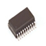
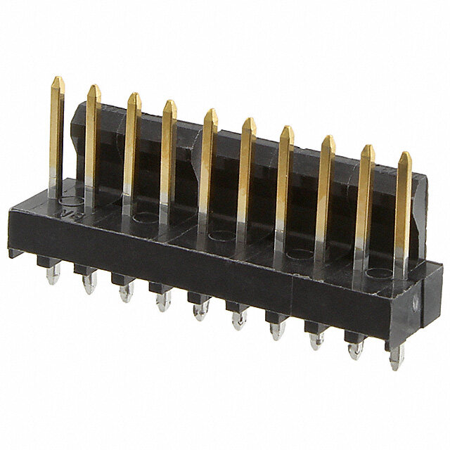
| 产品图片 |
|
| rohs | 符合RoHS无铅 / 符合限制有害物质指令(RoHS)规范要求 |
| 产品系列 | 嵌入式处理器和控制器,微控制器 - MCU,8位微控制器 -MCU,Freescale Semiconductor MC9S08JS8CWJS08 |
| 数据手册 | |
| 产品型号 | MC9S08JS8CWJ |
| PCN设计/规格 | http://cache.freescale.com/files/shared/doc/pcn/PCN16235.htm |
| RAM容量 | 512 x 8 |
| 产品目录页面 | |
| 产品种类 | 8位微控制器 -MCU |
| 供应商器件封装 | 20-SOIC W |
| 包装 | 管件 |
| 单位重量 | 519.500 mg |
| 可编程输入/输出端数量 | 14 |
| 商标 | Freescale Semiconductor |
| 处理器系列 | MC9S08 |
| 外设 | LVD,POR,PWM |
| 安装风格 | SMD/SMT |
| 定时器数量 | 1 Timer |
| 封装 | Tube |
| 封装/外壳 | 20-SOIC(0.295",7.50mm 宽) |
| 封装/箱体 | SOIC-20 Wide |
| 工作温度 | -40°C ~ 85°C |
| 工作电源电压 | 2.7 V to 5.5 V |
| 工厂包装数量 | 38 |
| 振荡器类型 | 内部 |
| 接口类型 | SCI, SPI |
| 数据RAM大小 | 256 B |
| 数据总线宽度 | 8 bit |
| 数据转换器 | - |
| 最大工作温度 | + 85 C |
| 最大时钟频率 | 48 MHz |
| 最小工作温度 | - 40 C |
| 标准包装 | 2,698 |
| 核心 | S08 |
| 核心处理器 | S08 |
| 核心尺寸 | 8-位 |
| 片上ADC | No |
| 电压-电源(Vcc/Vdd) | 2.7 V ~ 5.5 V |
| 电源电压-最大 | 5.5 V |
| 电源电压-最小 | 2.7 V |
| 程序存储器大小 | 16 kB |
| 程序存储器类型 | Flash |
| 程序存储容量 | 8KB(8K x 8) |
| 系列 | S08JS |
| 输入/输出端数量 | 14 I/O |
| 连接性 | LIN,SCI,SPI,USB |
| 速度 | 48MHz |


PDF Datasheet 数据手册内容提取
Freescale Semiconductor Document Number: QFN_Addendum Rev. 0, 07/2014 Addendum Addendum for New QFN Package Migration This addendum provides the changes to the 98A case outline numbers for products covered in this book. Case outlines were changed because of the migration from gold wire to copper wire in some packages. See the table below for the old (gold wire) package versus the new (copper wire) package. To view the new drawing, go to Freescale.com and search on the new 98A package number for your device. For more information about QFN package use, see EB806: Electrical Connection Recommendations for the Exposed Pad on QFN and DFN Packages. ©Freescale Semiconductor, Inc., 2014. All rights reserved.
Original (gold wire) Current (copper wire) Part Number Package Description package document number package document number MC68HC908JW32 48 QFN 98ARH99048A 98ASA00466D MC9S08AC16 MC9S908AC60 MC9S08AC128 MC9S08AW60 MC9S08GB60A MC9S08GT16A MC9S08JM16 MC9S08JM60 MC9S08LL16 MC9S08QE128 MC9S08QE32 MC9S08RG60 MCF51CN128 MC9RS08LA8 48 QFN 98ARL10606D 98ASA00466D MC9S08GT16A 32 QFN 98ARH99035A 98ASA00473D MC9S908QE32 32 QFN 98ARE10566D 98ASA00473D MC9S908QE8 32 QFN 98ASA00071D 98ASA00736D MC9S08JS16 24 QFN 98ARL10608D 98ASA00734D MC9S08QB8 MC9S08QG8 24 QFN 98ARL10605D 98ASA00474D MC9S08SH8 24 QFN 98ARE10714D 98ASA00474D MC9RS08KB12 24 QFN 98ASA00087D 98ASA00602D MC9S08QG8 16 QFN 98ARE10614D 98ASA00671D MC9RS08KB12 8 DFN 98ARL10557D 98ASA00672D MC9S08QG8 MC9RS08KA2 6 DFN 98ARL10602D 98ASA00735D Addendum for New QFN Package Migration, Rev. 0 2 Freescale Semiconductor
Freescale Semiconductor Document Number: MC9S08JS16 Data Sheet: Technical Data Rev. 4, 4/2009 MC9S08JS16 MC9S08JS16 Series 20 W-SOIC 24 QFN TBD Case 751D Case 1982-01 Covers: MC9S08JS16 MC9S08JS8 MC9S08JS16L MC9S08JS8L Features: – SPI — One 8- or 16-bit selectable serial peripheral • 8-Bit HCS08 Central Processor Unit (CPU) interface module with a receive data buffer hardware – 48 MHz HCS08 CPU (central processor unit) match function – 24 MHz internal bus frequency – SCI — One serial communications interface module – Support for up to 32 interrupt/reset sources with optional 13 bit break. Full duplex non-return to zero • Memory Options (NRZ); LIN master extended break generation; LIN – Up to 16 KB of on-chip in-circuit programmable flash slave extended break detection; wakeup on active edge memory with block protection and security options – MTIM — One 8-bit modulo counter with 8-bit prescaler – Up to 512 bytes of on-chip RAM and overflow interrupt – 256 bytes of USB RAM – TPM — One 2-channel 16-bit timer/pulse-width • Clock Source Options modulator (TPM) module; selectable input capture, – Clock source options include crystal, resonator, external output compare, and edge-aligned PWM capability on clock each channel; timer module may be configured for – MCG (multi-purpose clock generator) — PLL and FLL; buffered, centered PWM (CPWM) on all channels internal reference clock with trim adjustment – KBI — 8-pin keyboard interrupt module • System Protection – RTC — Real-time counter with binary- or – Optional computer operating properly (COP) reset with decimal-based prescaler option to run from independent 1 kHz internal clock – CRC — Hardware CRC generator circuit using 16-bit source or the bus clock shift register; CRC16-CCITT compliancy with – Low-voltage detection x16+x12+x5+1 polynomial – Illegal opcode detection with reset • Input/Output – Illegal address detection with reset – Software selectable pullups on ports when used as inputs • Power-Saving Modes – Software selectable slew rate control on ports when used – Wait plus two stops as outputs • USB Bootload – Software selectable drive strength on ports when used as – Mass erase entire flash array outputs – Partial erase flash array — erase all flash blocks except – Master reset pin and power-on reset (POR) for the first 1 KB of flash – Internal pullup on RESET, IRQ, and BKGD/MS pins to – Program flash reduce customer system cost • Peripherals • Package Options – USB — USB 2.0 full-speed (12 Mbps) with dedicated – 24-pin quad flat no-lead (QFN) on-chip 3.3 V regulator and transceiver; supports – 20-pin small outline IC package (SOIC) endpoint 0 and up to 6 additional endpoints This document contains information on a product under development. Freescale reserves the right to change or discontinue this product without notice. ©Freescale Semiconductor, Inc., 2008-2009. All rights reserved.
Table of Contents 1 MCU Block Diagram. . . . . . . . . . . . . . . . . . . . . . . . . . . . . . . . .3 3.9 AC Characteristics. . . . . . . . . . . . . . . . . . . . . . . . . . . . 19 2 Pin Assignments. . . . . . . . . . . . . . . . . . . . . . . . . . . . . . . . . . . .4 3.9.1 Control Timing . . . . . . . . . . . . . . . . . . . . . . . . . 19 3 Electrical Characteristics . . . . . . . . . . . . . . . . . . . . . . . . . . . . .6 3.9.2 Timer/PWM (TPM) Module Timing. . . . . . . . . . 20 3.1 Parameter Classification. . . . . . . . . . . . . . . . . . . . . . . . .6 3.10 SPI Characteristics . . . . . . . . . . . . . . . . . . . . . . . . . . . 21 3.2 Absolute Maximum Ratings . . . . . . . . . . . . . . . . . . . . . .6 3.11 Flash Specifications. . . . . . . . . . . . . . . . . . . . . . . . . . . 24 3.3 Thermal Characteristics . . . . . . . . . . . . . . . . . . . . . . . . .7 3.12 USB Electricals . . . . . . . . . . . . . . . . . . . . . . . . . . . . . . 25 3.4 Electrostatic Discharge (ESD) Protection Characteristics8 4 Ordering Information. . . . . . . . . . . . . . . . . . . . . . . . . . . . . . . 26 3.5 DC Characteristics . . . . . . . . . . . . . . . . . . . . . . . . . . . . .8 4.1 Package Information . . . . . . . . . . . . . . . . . . . . . . . . . . 26 3.6 Supply Current Characteristics. . . . . . . . . . . . . . . . . . .15 4.2 Mechanical Drawings. . . . . . . . . . . . . . . . . . . . . . . . . . 26 3.7 External Oscillator (XOSC) Characteristics . . . . . . . . .17 3.8 MCG Specifications . . . . . . . . . . . . . . . . . . . . . . . . . . .18 Revision History To provide the most up-to-date information, the revision of our documents on the World Wide Web will be the most current. Your printed copy may be an earlier revision. To verify you have the latest information available, refer to: http://freescale.com/ The following revision history table summarizes changes contained in this document. Revision Date Description of Changes 1 9/1/2008 Initial public released In Table7, changed the parameter description of RI and S3I the typicals of 2 1/8/2009 DD DD, RI were changed as well. DD 3 3/9/2009 Corrected the 24-pin QFN case number and doc. number information. 4 4/24/2009 Added new parts information about MC9S08JS16L and MC9S08JS8L. Related Documentation Find the most current versions of all documents at: http://www.freescale.com Reference Manual (MC9S08JS16RM) Contains extensive product information including modes of operation, memory, resets and interrupts, register definition, port pins, CPU, and all module information. MC9S08JS16 Series MCU Data Sheet, Rev. 4 2 Freescale Semiconductor
MCU Block Diagram 1 MCU Block Diagram The block diagram, Figure 1, shows the structure of the MC9S08JS16 series MCU. ON-CHIP ICE AND HCS08 CORE DEBUG MODULE (DBG) USBDP USBDN USB BKGD/MS MODULE FULL SPEED BDC CPU USB USB ENDPOINT TRANSCEIVER RAM PTA0/KBIP0/TPMCH0 RESET HCS08 SYSTEM CONTROL PTA1/KBIP1/MISO 8-BIT KEYBOARD KBIPx 8 RESETS AND INTERRUPTS INTERRUPT MODULE (KBI) PTA2/KBIP2/MOSI MODES OF OPERATION IRQ POWER MANAGEMENT MISO A PTA3/KBIP3/SPSCK T 8-/16-BIT MOSI R O COP IRQ LVD SERIAL PERIPHERAL SPSCK P PTA4/KBIP4/SS INTERFACE MODULE (SPI) SS PTA5/KBIP5/TPMCH1 USER FLASH (IN BYTES) MC9S08JS16 = 16,384 RxD MC9S08JS16L = 16,384 SERIAL COMMUNICATIONS PTA6/KBIP6/RxD MC9S08JS8 = 8,192 INTERFACE MODULE (SCI) TxD MC9S08JS8L = 8,192 PTA7/KBIP7/TxD TPMCH0 USER RAM (IN BYTES) 2-CHANNEL TIMER/PWM TPMCH1 512 MODULE (TPM) TCLK PTB0/IRQ/TCLK PTB1/RESET PTB2/BKGD/MS Bootloader ROM (IN BYTES) PTB3/BLMS 4096 8-BIT MODULO TIMER B MODULE (MTIM) T R O MULTI-PURPOSE CLOCK EXTAL P PTB4/XTAL GENERATOR (MCG) XTAL PTB5/EXTAL VSSOSC LOW-POWER OSCILLATOR 16-BIT Cyclic Redundancy Check Generator VDD SYSTEM MODULE (CRC) VOLTAGE VSS REGULATOR VUSB33 USB 3.3 V VOLTAGE REGULATOR REAL-TIME COUNTER (RTC) NOTES: 1. Port pins are software configurable with pullup device if input port. 2. Pin contains software configurable pullup/pulldown device if IRQ is enabled (IRQPE=1). Pulldown is enabled if rising edge detect is selected (IRQEDG = 1). 3. IRQ does not have a clamp diode to V . IRQ must not be driven above V . DD DD 4. RESET contains integrated pullup device if PTB1 enabled as reset pin function (RSTPE = 1). 5. Pin contains integrated pullup device. 6. When pin functions as KBI (KBIPEn = 1) and associated pin is configured to enable the pullup device, KBEDGn can be used to reconfigure the pullup as a pulldown device. Figure1. MC9S08JS16 Series Block Diagram MC9S08JS16 Series MCU Data Sheet, Rev. 4 Freescale Semiconductor 3
Pin Assignments 2 Pin Assignments This section shows the pin assignments in the packages available for the MC9S08JS16 series. Table1. Pin Availability by Package Pin-Count Pin Number <-- Lowest Priority --> Highest (Package) 24 (QFN) 20 (SOIC) Port Pin Alt 1 Alt 2 1 4 PTB0 IRQ TCLK 2 5 PTB1 RESET 3 6 PTB2 BKGD MS 4 7 PTB3 BLMS 5 8 PTA0 KBIP0 TPMCH0 6 — NC 7 9 PTA1 KBIP1 MISO 8 10 PTA2 KBIP2 MOSI 9 11 PTA3 KBIP3 SPSCK 10 12 PTA4 KBIP4 SS 11 13 V DD 12 — NC 13 14 V SS 14 15 USBDN 15 16 USBDP 16 17 V USB33 17 18 PTA5 KBIP5 TPMCH1 18 — NC 19 19 PTA6 KBIP6 RxD 20 20 PTA7 KBIP7 TxD 21 1 PTB4 XTAL 22 2 PTB5 EXTAL 23 3 V SSOSC 24 — NC MC9S08JS16 Series MCU Data Sheet, Rev. 4 4 Freescale Semiconductor
Pin Assignments D D Tx Rx XTAL TAL BIP7/ BIP6/ C E X K K C SSOS TB5/ TB4/ TA7/ TA6/ N V P P P P 24 23 22 21 20 19 PTB0/IRQ/TCLK 1 18 NC PTB1/RESET 2 17 PTA5/KBIP5/TPMCH1 PTB2/BKGD/MS 3 16 VUSB33 24-Pin QFN 15 USBDP PTB3/BLMS 4 14 USBDN PTA0/KBIP0/TPMCH0 5 NC 6 13 VVSSSS 7 8 9 10 11 12 1/KBIP1/MISO 2/KBIP2/MOSI KBIP3/SPSCK TA4/KBIP4/SS VDD NC TA TA A3/ P P P T P Figure2. MC9S08JS16 Series in 24-QFN Package PTB4/XTAL 1 20 PTA7/KBIP7/TxD PTB5/EXTAL 2 19 PTA6/KBIP6/RxD V 3 18 PTA5/KBIP5/TPMCH1 SSOSC PTB0/IRQ/TCLK 4 17 V USB33 PTB1/RESET 5 16 USBDP PTB2/BKGD/MS 6 15 USBDN PTB3/BLMS 7 14 VSS PTA0/KBIP0/TPMCH0 8 13 V DD PTA1/KBIP1/MISO 9 12 PTA4/KBIP4/SS PTA2/KBIP2/MOSI 10 11 PTA3/KBIP3/SPSCK Figure3. MC9S08JS16 Series in 20-pin SOIC Package MC9S08JS16 Series MCU Data Sheet, Rev. 4 Freescale Semiconductor 5
Electrical Characteristics 3 Electrical Characteristics This chapter contains electrical and timing specifications. 3.1 Parameter Classification The electrical parameters shown in this supplement are guaranteed by various methods. To give the customer a better understanding, the following classification is used and the parameters are tagged accordingly in the tables where appropriate: Table2. Parameter Classifications P Those parameters are guaranteed during production testing on each individual device. C Those parameters are achieved by the design characterization by measuring a statistically relevant sample size across process variations. T Those parameters are achieved by design characterization on a small sample size from typical devices under typical conditions unless otherwise noted. All values shown in the typical column are within this category. D Those parameters are derived mainly from simulations. NOTE The above classifications are used in the column labeled “C” in applicable tables of this data sheet. 3.2 Absolute Maximum Ratings Absolute maximum ratings are stress ratings only, and functional operation at the maximum is not guaranteed. Stress beyond the limits specified in Table 3 may affect device reliability or cause permanent damage to the device. For functional operating conditions, refer to the remaining tables in this section. This device contains circuitry protecting against damage due to high static voltage or electrical fields; however, it is advised that normal precautions be taken to avoid application of any voltages higher than maximum-rated voltages to this high-impedance circuit. Reliability of operation is enhanced if unused inputs are tied to an appropriate logic voltage level (for instance, either V or V ). SS DD Table3. Absolute Maximum Ratings Rating Symbol Value Unit Supply voltage V 2.7 to 5.5 V DD Input voltage V –0.3 to V + 0.3 V In DD Instantaneous maximum current Single pin limit (applies to all port pins)1,2,3 ID ±25 mA Maximum current into V I 120 mA DD DD Storage temperature Tstg –55 to 150 °C Maximum junction temperature T 150 °C J MC9S08JS16 Series MCU Data Sheet, Rev. 4 6 Freescale Semiconductor
Electrical Characteristics 1 Input must be current limited to the value specified. To determine the value of the required current-limiting resistor, calculate resistance values for positive (V ) and negative (V ) clamp DD SS voltages, then use the larger of the two resistance values. 2 All functional non-supply pins are internally clamped to V and V . SS DD 3 Power supply must maintain regulation within operating V range during instantaneous and DD operating maximum current conditions. If positive injection current (V > V ) is greater than In DD I , the injection current may flow out of V and could result in external power supply going DD DD out of regulation. Ensure external V load will shunt current greater than maximum injection DD current. This will be the greatest risk when the MCU is not consuming power. Examples are: if no system clock is present, or if the clock rate is very low which would reduce overall power consumption. 3.3 Thermal Characteristics This section provides information about operating temperature range, power dissipation, and package thermal resistance. Power dissipation on I/O pins is usually small compared to the power dissipation in on-chip logic and it is user-determined rather than being controlled by the MCU design. In order to take P into account in power calculations, determine the difference between actual pin voltage and V or I/O SS V and multiply by the pin current for each I/O pin. Except in cases of unusually high pin current (heavy DD loads), the difference between pin voltage and V or V will be very small. SS DD Table4. Thermal Characteristics Rating Symbol Value Unit Operating temperature range (packaged) T to T TA L H °C -40 to 85 Thermal resistance 1,2,3,4 24-pin QFN 1s 92 θ °C/W 2s2p JA 33 20-pin SOIC 1s 86 2s2p 58 1 Junction temperature is a function of die size, on-chip power dissipation, package thermal resistance, mounting site (board) temperature, ambient temperature, air flow, power dissipation of other components on the board, and board thermal resistance 2 Junction to Ambient Natural Convection 3 1s — Single layer board, one signal layer 4 2s2p — Four layer board, 2 signal and 2 power layers The average chip-junction temperature (T ) in °C can be obtained from: J T = T + (P × θ ) Eqn.1 J A D JA where: T = Ambient temperature, °C A θ = Package thermal resistance, junction-to-ambient, °C/W JA MC9S08JS16 Series MCU Data Sheet, Rev. 4 Freescale Semiconductor 7
Electrical Characteristics P = P + P P = I × V , Watts — chip internal power D int I/O int DD DD P = Power dissipation on input and output pins — user determined I/O For most applications, P << P and can be neglected. An approximate relationship between P and T I/O int D J (if P is neglected) is: I/O P = K ÷ (T + 273°C) Eqn.2 D J Solving Equation1 and Equation2 for K gives: K = P × (T + 273°C) + θ × (P )2 Eqn.3 D A JA D where K is a constant pertaining to the particular part. K can be determined from Equation3 by measuring P (at equilibrium) for a known T . Using this value of K, the values of P and T can be obtained by D A D J solving Equation1 and Equation2 iteratively for any value of T . A 3.4 Electrostatic Discharge (ESD) Protection Characteristics Although damage from static discharge is much less common on these devices than on early CMOS circuits, normal handling precautions must be used to avoid exposure to static discharge. Qualification tests are performed to ensure that these devices can withstand exposure to reasonable levels of static without suffering any permanent damage. This device was qualified to AEC-Q100 Rev E. A device is considered to have failed if, after exposure to ESD pulses, the device no longer meets the device specification requirements. Complete DC parametric and functional testing is performed per the applicable device specification at room temperature followed by hot temperature, unless specified otherwise in the device specification. Table5. ESD Protection Characteristics Parameter Symbol Value Unit ESD Target for Machine Model (MM) — MM circuit V 200 V description THMM ESD Target for Human Body Model (HBM) — HBM V 2000 V circuit description THHBM 3.5 DC Characteristics This section includes information about power supply requirements, I/O pin characteristics, and power supply current in various operating modes. Table6. DC Characteristics Num C Parameter Symbol Min Typical1 Max Unit 1 Operating voltage2 — 2.7 — 5.5 V MC9S08JS16 Series MCU Data Sheet, Rev. 4 8 Freescale Semiconductor
Electrical Characteristics Table6. DC Characteristics (continued) Num C Parameter Symbol Min Typical1 Max Unit Output high voltage — Low drive (PTxDSn = 0) 5 V, I = –2 mA V – 1.5 — — Load DD 3 V, I = –0.6 mA V – 1.5 — — Load DD 5 V, I = –0.4 mA V – 0.8 — — Load DD 3 V, I = –0.24 mA V – 0.8 — — Load DD 2 P V V OH Output high voltage — High drive (PTxDSn = 1) 5 V, I = –10 mA V – 1.5 — — Load DD 3 V, I = –3 mA V – 1.5 — — Load DD 5 V, I = –2 mA V – 0.8 — — Load DD 3 V, I = –0.4 mA V – 0.8 — — Load DD Output low voltage — Low drive (PTxDSn = 0) 5 V, I = 2 mA 1.5 — — Load 3 V, I = 0.6 mA 1.5 — — Load 5 V, I = 0.4 mA 0.8 — — Load 3 V, I = 0.24 mA 0.8 — — Load 3 P V V OL Output low voltage — High drive (PTxDSn = 1) 5 V, I = 10 mA 1.5 — — Load 3 V, I = 3 mA 1.5 — — Load 5 V, I = 2 mA 0.8 — — Load 3 V, I = 0.4 mA 0.8 — — Load Output high current — Max total I for all ports OH 4 P 5 V I — — 100 mA OHT 3 V — — 60 Output low current — Max total I for all ports OL 5 P 5 V I — — 100 mA OLT 3 V — — 60 6 P Input high voltage; all digital inputs V 0.65 × V — — IH DD V 7 P Input low voltage; all digital inputs V — — 0.35 × V IL DD 8 P Input hysteresis; all digital inputs V 0.06 × V — — mV hys DD 9 P Input leakage current; input only pins3 |I | — 0.1 1 μA In 10 P High Impedance (off-state) leakage current3 |I | — 0.1 1 μA OZ 11 P Internal pullup resistors4 R 20 45 65 kΩ PU 12 P Internal pulldown resistors5 R 20 45 65 kΩ PD Internal pullup resistor to USBDP (to V ) USB33 — 13 C Idle R 900 1575 kΩ PUPD — Transmit 1425 3090 14 C Input capacitance; all non-supply pins C — — 8 pF In 15 C RAM retention voltage V 0.6 1.0 — V RAM 16 P POR rearm voltage V 0.9 1.4 2.0 V POR 17 D POR rearm time t 10 — — μs POR MC9S08JS16 Series MCU Data Sheet, Rev. 4 Freescale Semiconductor 9
Electrical Characteristics Table6. DC Characteristics (continued) Num C Parameter Symbol Min Typical1 Max Unit Low-voltage detection threshold — high range 18 P V V V falling LVD1 3.9 4.0 4.1 DD V rising 4.0 4.1 4.2 DD Low-voltage detection threshold — low range 19 P V V V falling LVD0 2.48 2.56 2.64 DD V rising 2.54 2.62 2.70 DD Low-voltage warning threshold — high range 1 20 C V V V falling LVW3 4.5 4.6 4.7 DD V rising 4.6 4.7 4.8 DD Low-voltage warning threshold — high range 0 21 P V V V falling LVW2 4.2 4.3 4.4 DD V rising 4.3 4.4 4.5 DD Low-voltage warning threshold low range 1 22 P V V V falling LVW1 2.84 2.92 3.00 DD V rising 2.90 2.98 3.06 DD Low-voltage warning threshold — low range 0 23 C V V V falling LVW0 2.66 2.74 2.82 DD V rising 2.72 2.80 2.88 DD Low-voltage inhibit reset/recover hysteresis 24 T 5 V V — 100 — mV hys 3 V — 60 — 1 Typical values are based on characterization data at 25 °C unless otherwise stated. 2 Operating voltage with USB enabled can be found in Section3.11, “USB Electricals.” 3 Measured with V = V or V . In DD SS 4 Measured with V = V . In SS 5 Measured with V = V . In DD MC9S08JS16 Series MCU Data Sheet, Rev. 4 10 Freescale Semiconductor
Electrical Characteristics I vs V -V (Low Drive) at V = 3 V OH DD OH DD 0.30 0.25 V) 0.20 -40C (H O 0.15 25C V -DD 0.10 85C V 0.05 0.00 0 -0.2 -0.4 -0.6 -0.8 -1 -1.2 -1.4 -1.6 -1.8 -2 -2.2 -2.4 -2.6 -2.8 -3 I (mA) OH Figure4. Typical I (Low Drive) vs V –V at V = 3 V OH DD OH DD I vs V -V (High Drive) at V = 3 V OH DD OH DD 0.40 0.35 0.30 ) V 0.25 -40C (H O 0.20 25C V -DD 0.15 85C V 0.10 0.05 0.00 0 -1 -2 -3 -4 -5 -6 -7 -8 -9 -10 -11 -12 -13 -14 -15 I (mA) OH Figure5. Typical I (High Drive) vs V –V at V = 3 V OH DD OH DD MC9S08JS16 Series MCU Data Sheet, Rev. 4 Freescale Semiconductor 11
Electrical Characteristics I vs V -V (Low Drive) at V = 5 V OH DD OH DD 0.7 0.6 0.5 ) -40C V 0.4 (L 25C O 0.3 V 85C 0.2 0.1 0.0 0 -0.2 -0.4 -0.6 -0.8 -1 -1.2 -1.4 -1.6 -1.8 -2 -2.2 -2.4 -2.6 -2.8 -3 I (mA) OH Figure6. Typical I (Low Drive) vs V –V at V = 5 V OH DD OH DD I vs V -V (High Drive) at V = 5 V OH DD OH DD 0.8 0.7 0.6 ) V 0.5 -40C (H O 0.4 25C V -DD 0.3 85C V 0.2 0.1 0.0 0 -1 -2 -3 -4 -5 -6 -7 -8 -9 -10 -11 -12 -13 -14 -15 I (mA) OH Figure7. Typical I (High Drive) vs V –V at V = 5 V OH DD OH DD MC9S08JS16 Series MCU Data Sheet, Rev. 4 12 Freescale Semiconductor
Electrical Characteristics I vs V (Low Drive) at V = 5 V OL OL DD 0.14 0.12 0.10 V) 0.08 -40C (OL 0.06 25C V 85C 0.04 0.02 0.00 0 2 4 6 8 1 2 4 6 8 2 2 4 6 8 3 0. 0. 0. 0. - 1. 1. 1. 1. - 2. 2. 2. 2. - - - - - - - - - - - - - I (mA) OL Figure8. I vs V (Low Drive) at V = 5 V OL OL DD I vs V (High Drive) at V = 5 V OL OL DD 0.25 0.20 V) 0.15 -40C (L 25C VO 0.10 85C 0.05 0.00 0 -1 -2 -3 -4 -5 -6 -7 -8 -9 -10 -11 -12 -13 -14 -15 I (mA) OL Figure9. I vs V (High Drive) at V = 5 V OL OL DD MC9S08JS16 Series MCU Data Sheet, Rev. 4 Freescale Semiconductor 13
Electrical Characteristics I vs V (Low Drive) at V = 3 V OL OL DD 1.0 0.8 V) 0.6 -40C (L 25C VO 0.4 85C 0.2 0.0 0 -0.2 -0.4 -0.6 -0.8 -1 -1.2 -1.4 -1.6 -1.8 -2 -2.2 -2.4 -2.6 -2.8 -3 I (mA) OL Figure10. I vs V (Low Drive) at V = 3 V OL OL DD I vs V (High Drive) at V = 3 V OL OL DD 1.4 1.2 1.0 V) 0.8 -40C (L 25C O 0.6 V 85C 0.4 0.2 0.0 0 -1 -2 -3 -4 -5 -6 -7 -8 -9 -10 -11 -12 -13 -14 -15 I (mA) OL Figure11. I vs V (High Drive) at V = 3 V OL OL DD MC9S08JS16 Series MCU Data Sheet, Rev. 4 14 Freescale Semiconductor
Electrical Characteristics 3.6 Supply Current Characteristics Table7. Supply Current Characteristics Num C Parameter Symbol V (V) Typical1 Max2 Unit DD Run supply current3 measured at (CPU clock 5 1.03 — 1 C RI mA = 2MHz, fBus = 1 MHz, BLPE mode) DD 3 0.83 — Run supply current3 measured at (CPU 5 19.93 — 2 P clock = 48MHz, f = 24 MHz, PEE mode, all RI mA Bus DD module on) 3 18.74 — Stop2 mode supply current 5 1.36 — μA 3 P S2I DD 3 1.18 — μA 5 1.50 — μA 4 P Stop3 mode supply current, all module off S3I DD 3 1.31 — μA 5 300 — nA 5 P RTC adder to stop2 or stop33, 25 °C ΔI SRTC 3 300 — nA 5 106.7 — μA 6 P LVD adder to stop3 (LVDE = LVDSE = 1) ΔI SLVD 3 95.6 — μA Adder to stop3 for oscillator enabled4 5 5.6 — μA 7 P ΔI (ERCLKEN =1 and EREFSTEN = 1) SOSC 3 5.3 — μA 8 T USB module enable current5 ΔI 5 1.5 — mA USBE 9 T USB suspend current6 I 5 273.3 — μA SUSP 1 Typicals are measured at 25 °C. See Figure12 through Figure10 for typical curves across voltage/temperature. 2 Values given here are preliminary estimates prior to completing characterization. 3 Most customers are expected to find that auto-wakeup from stop2 or stop3 can be used instead of the higher current wait mode. Wait mode typical is 560 μA at 5 V and 422 μA at 3 V with f = 1 MHz. Bus 4 Values given under the following conditions: low range operation (RANGE = 0), low power mode (HGO = 0). 5 Here USB module is enabled and clocked at 48 MHz (USBEN = 1, USBVREN =1, USBPHYEN = 1 and USBPU = 1), and D+ and D– pulled down by two 15.1 kΩ resisters independently. The current consumption may be much higher when the packets are being transmitted through the attached cable. 6 MCU enters stop3 mode, USB bus in idle state. The USB suspend current will be dominated by the D+ pullup resister. MC9S08JS16 Series MCU Data Sheet, Rev. 4 Freescale Semiconductor 15
Electrical Characteristics Typical Run I for PEE,FBE & BLPE I vs. V DD DD DD 25.000 20.000 A) 15.000 PEE,48MHz Core m FBE,8MHz Core (D ID 10.000 BLPE,2MHz Core 5.000 0.000 2.5 3 3.5 4 4.5 5 5.5 VDD(V) Figure12. Typical Run I for PEE, FBE and BLPE Modes (I vs. V ) DD DD DD MC9S08JS16 Series MCU Data Sheet, Rev. 4 16 Freescale Semiconductor
Electrical Characteristics 3.7 External Oscillator (XOSC) Characteristics Table8. Oscillator Electrical Specifications (Temperature Range = –40 to 85°C Ambient) Num C Rating Symbol Min Typ1 Max Unit Oscillator crystal or resonator (EREFS=1, ERCLKEN = 1) Low range (RANGE = 0) f 32 — 38.4 kHz lo High range (RANGE = 1) FEE or FBE mode2 f 1 — 5 MHz 1 C hi-fll High range (RANGE = 1) PEE or PBE mode3 f 1 — 16 MHz hi-pll High range (RANGE = 1, HGO = 1) BLPE mode f 1 — 16 MHz hi-hgo High range (RANGE = 1, HGO = 0) BLPE mode f 1 — 8 MHz hi-lp See crystal or resonator 2 — Load capacitors C C 1, 2 manufacturer’s recommendation. Feedback resistor 3 — Low range (32 kHz to 38.4 kHz) R — 10 — F MΩ High range (1 MHz to 16 MHz) — 1 — Series resistor Low range, low gain (RANGE = 0, HGO = 0) — 0 — Low range, high gain (RANGE = 0, HGO = 1) — 100 — High range, low gain (RANGE = 1, HGO = 0) — 0 — 4 — R kΩ High range, high gain (RANGE = 1, HGO = 1) S ≥ 8 MHz — 0 0 4 MHz — 0 10 1 MHz — 0 20 Crystal start-up time4 Low range, low gain (RANGE = 0, HGO = 0) t — 200 — CSTL-LP 5 T Low range, high gain (RANGE = 0, HGO = 1) t — 400 — CSTL-HGO ms High range, low gain (RANGE = 1, HGO = 0)5 t — 5 — CSTH-LP High range, high gain (RANGE = 1, HGO = 1)5 t — 15 — CSTH-HGO Square wave input clock frequency (EREFS=0, ERCLKEN = 1) FEE or FBE mode2 0.03125 — 5 6 T f PEE or PBE mode3 extal 1 — 16 MHz BLPE mode 0 — 40 1 Typical data was characterized at 3.0 V, 25 °C or is recommended value. 2 When MCG is configured for FEE or FBE mode, input clock source must be divided using RDIV to within the range of 31.25 kHz to 39.0625 kHz. 3 When MCG is configured for PEE or PBE mode, input clock source must be divided using RDIV to within the range of 1 MHz to 2 MHz. 4 This parameter is characterized and not tested on each device. Proper PC board layout procedures must be followed to achieve specifications. 5 4 MHz crystal. MCU EXTAL XTAL R R S F C1 Crystal or Resonator C2 MC9S08JS16 Series MCU Data Sheet, Rev. 4 Freescale Semiconductor 17
Electrical Characteristics 3.8 MCG Specifications Table9. MCG Frequency Specifications(Te mperature Range = –40 to 85°C Ambient) Num C Rating Symbol Min Typical Max Unit 1 C Average internal reference frequency — untrimmed fint_ut 25 32.7 41.66 kHz 2 P Average internal reference frequency — trimmed fint_t 31.25 — 39.0625 kHz 3 T Internal reference startup time tirefst — 60 100 μs 4 C DCO output frequency range — untrimmed fdco_ut 25.6 33.48 42.66 MHz 5 P DCO output frequency range — trimmed fdco_t 32 — 40 MHz Resolution of trimmed DCO output frequency at 6 C fixed voltage and temperature (using FTRIM) Δfdco_res_t — ±0.1 ±0.2 %fdco Resolution of trimmed DCO output frequency at 7 C fixed voltage and temperature (not using FTRIM) Δfdco_res_t — ±0.2 ±0.4 %fdco Total deviation of trimmed DCO output frequency 0.5 8 P over voltage and temperature Δfdco_t — –1.0 ±2 %fdco Total deviation of trimmed DCO output frequency 9 C over fixed voltage and temperature range of Δfdco_t — ±0.5 ±1 %fdco 0–70 °C 10 C FLL acquisition time1 tfll_acquire — — 1 ms 11 D PLL acquisition time2 tpll_acquire — — 1 ms Long term Jitter of DCO output clock (averaged over 12 C 2ms interval)3 CJitter — 0.02 0.2 %fdco 13 D VCO operating frequency fvco 7.0 — 55.0 MHz 14 D PLL reference frequency range fpll_ref 1.0 — 2.0 MHz Long term accuracy of PLL output clock (averaged 15 T over 2 ms) fpll_jitter_2ms — 0.5904 — % 16 T Jitter of PLL output clock measured over 625 ns5 fpll_jitter_625ns — 0.5664 — % 17 D Lock entry frequency tolerance6 Dlock ±1.49 — ±2.98 % 18 D Lock exit frequency tolerance7 Dunl ±4.47 — ±5.97 % t 19 D Lock time — FLL tfll_lock — — fll_acqfuire+ s 1075(1/int_t) t 20 D Lock time — PLL tpll_lock — — pll_acfquire+ s 1075(1/pll_ref) Loss of external clock minimum frequency — 21 D RANGE = 0 floc_low (3/5) x fint — — kHz Loss of external clock minimum frequency — 22 D RANGE = 1 floc_high (16/5) x fint — — kHz 1 This specification applies any time the FLL reference source or reference divider is changed, trim value changed or changing from FLL disabled (BLPE, BLPI) to FLL enabled (FEI, FEE, FBE, FBI). If a crystal/resonator is being used as the reference, this specification assumes it is already running. 2 This specification applies to any time the PLL VCO divider or reference divider is changed, or changing from PLL disabled (BLPE, BLPI) to PLL enabled (PBE, PEE). If a crystal/resonator is being used as the reference, this specification assumes it is already running. MC9S08JS16 Series MCU Data Sheet, Rev. 4 18 Freescale Semiconductor
Electrical Characteristics 3 Jitter is the average deviation from the programmed frequency measured over the specified interval at maximum f . BUS Measurements are made with the device powered by filtered supplies and clocked by a stable external clock signal. Noise injected into the FLL circuitry via V and V and variation in crystal oscillator frequency increase the C percentage for DD SS Jitter a given interval. 4 Jitter measurements are based upon a 48 MHz clock frequency. 5 625 ns represents 5 time quanta for CAN applications, under worst case conditions of 8 MHz CAN bus clock, 1 Mbps CAN bus speed, and 8 time quanta per bit for bit time settings. 5 time quanta is the minimum time between a synchronization edge and the sample point of a bit using 8 time quanta per bit. 6 Below D minimum, the MCG is guaranteed to enter lock. Above D maximum, the MCG will not enter lock. But if the MCG lock lock is already in lock, then the MCG may stay in lock. 7 Below D minimum, the MCG will not exit lock if already in lock. Above D maximum, the MCG is guaranteed to exit lock. unl unl 3.9 AC Characteristics This section describes AC timing characteristics for each peripheral system. 3.9.1 Control Timing Figure13. Con trol Timing Num C Parameter Symbol Min Typical1 Max Unit 1 D Bus frequency (t = 1/f ) f DC — 24 MHz cyc Bus Bus 2 D Internal low-power oscillator period t 700 — 1300 μs LPO External reset pulse width2 3 D t 1.5 × t — — ns (t = 1/f ) extrst Self_reset cyc Self_reset 4 D Reset low drive t 66 × t — — ns rstdrv cyc Active background debug mode latch setup 5 D t 25 — — ns time MSSU Active background debug mode latch hold 6 D t 25 — — ns time MSH IRQ pulse width 7 D Asynchronous path2 t t 100 ILIH, IHIL — — ns Synchronous path3 1.5 × t cyc KBIPx pulse width 8 D Asynchronous path2 t t 100 ILIH, IHIL — — ns Synchronous path3 1.5 × t cyc Port rise and fall time (load = 50 pF)4 9 C Slew rate control disabled (PTxSE = 0) t , t — 3 — ns Rise Fall Slew rate control enabled (PTxSE = 1) — 30 — 1 Typical values are based on characterization data at V = 5.0 V, 25 °C unless otherwise stated. DD 2 This is the shortest pulse that is guaranteed to be recognized as a reset pin request. Shorter pulses are not guaranteed to override reset requests from internal sources. 3 This is the minimum pulse width guaranteed to pass through the pin synchronization circuitry. Shorter pulses may or may not be recognized. In stop mode, the synchronizer is bypassed so shorter pulses can be recognized in that case. 4 Timing is shown with respect to 20% V and 80% V levels. Temperature range –40°C to 85°C. DD DD MC9S08JS16 Series MCU Data Sheet, Rev. 4 Freescale Semiconductor 19
Electrical Characteristics t extrst RESET PIN Figure14. Reset Timing t IHIL IRQ/KBIPx IRQ/KBIPx t ILIH Figure15. IRQ/KBIPx Timing 3.9.2 Timer/PWM (TPM) Module Timing Synchronizer circuits determine the shortest input pulses that can be recognized or the fastest clock that can be used as the optional external source to the timer counter. These synchronizers operate from the current bus rate clock. Table10. TPM Input Timing Num C Function Symbol Min Max Unit 1 D External clock frequency f dc f /4 MHz TPMext Bus 2 D External clock period t 4 — t TPMext cyc 3 D External clock high time t 1.5 — t clkh cyc 4 D External clock low time t 1.5 — t clkl cyc 5 D Input capture pulse width t 1.5 — t ICPW cyc t TPMext t clkh TPMxCLK t clkl Figure16. Timer External Clock MC9S08JS16 Series MCU Data Sheet, Rev. 4 20 Freescale Semiconductor
Electrical Characteristics t ICPW TPMxCHn TPMxCHn t ICPW Figure17. Timer Input Capture Pulse 3.10 SPI Characteristics Table 11 and Figure 18 through Figure 21 describe the timing requirements for the SPI system. MC9S08JS16 Series MCU Data Sheet, Rev. 4 Freescale Semiconductor 21
Electrical Characteristics Table11. SPI Electrical Characteristic Num1 C Characteristic2 Symbol Min Typical Max Unit Operating frequency3 1 D Master f — f /2 op f /2048DC Bus Hz Slave f Bus — f /4 op Bus Cycle time 2 D Master t 2 — 2048 t SCK cyc Slave t 4 — — SCK Enable lead time 3 D Master t — 1/2 — t Lead SCK Slave t — 1/2 — Lead Enable lag time 4 D Master t — 1/2 — t Lag SCK Slave t — 1/2 — Lag Clock (SPSCK) high time 5 D Master — 1/2 t — ns t SCK Slave SCKH 1/2 t – 25 1/2 t — SCK SCK Clock (SPSCK) low time 6 D Master — 1/2 t — ns t SCK Slave SCKL 1/2 t – 25 1/2 t — SCK SCK Data setup time (inputs) 7 D Master t 30 — — ns SI(M) Slave t 30 — — SI(S) Data hold time (inputs) 8 D Master t 30 — — ns HI(M) Slave t 30 — — HI(S) 9 D Access time, slave4 t — — 40 ns A 10 D Disable time, slave5 t — — 40 ns dis Data setup time (outputs) 11 D Master t — — 25 ns SO Slave t — — 25 SO Data hold time (outputs) 12 D Master t –10 — — ns HO Slave t –10 — — HO 1 Refer to Figure18 through Figure21. 2 All timing is shown with respect to 20% V and 80% V , unless noted; 50 pF load on all SPI pins. All timing assumes slew DD DD rate control disabled and high drive strength enabled for SPI output pins. 3 The maximum frequency is 8 MHz when input filter on SPI pins is disabled. 4 Time to data active from high-impedance state. 5 Hold time to high-impedance state. MC9S08JS16 Series MCU Data Sheet, Rev. 4 22 Freescale Semiconductor
Electrical Characteristics SS1 (OUTPUT) 2 1 3 SCK 5 (CPOL = 0) (OUTPUT) 4 SCK 5 (CPOL = 1) 4 (OUTPUT) 6 7 MISO (INPUT) MSB IN2 BIT 6 . . . 1 LSB IN 10 10 12 MOSI MSB OUT2 BIT 6 . . . 1 LSB OUT (OUTPUT) NOTES: 1. SS output mode (MODFEN = 1, SSOE = 1). 2. LSBF = 0. For LSBF = 1, bit order is LSB, bit 1, ..., bit 6, MSB. Figure18. SPI Master Timing (CPHA = 0) SS(1) (OUTPUT) 1 2 3 SCK 5 (CPOL = 0) (OUTPUT) 4 SCK 5 (CPOL = 1) 4 (OUTPUT) 6 7 MISO (INPUT) MSB IN(2) BIT 6 . . . 1 LSB IN 10 12 MOSI MSB OUT(2) BIT 6 . . . 1 LSB OUT (OUTPUT) NOTES: 1. SS output mode (MODFEN = 1, SSOE = 1). 2. LSBF = 0. For LSBF = 1, bit order is LSB, bit 1, ..., bit 6, MSB. Figure19. SPI Master Timing (CPHA = 1) MC9S08JS16 Series MCU Data Sheet, Rev. 4 Freescale Semiconductor 23
Electrical Characteristics SS (INPUT) 1 3 SCK 5 (CPOL = 0) (INPUT) 4 2 SCK 5 (CPOL = 1) (INPUT) 4 9 8 10 12 MISO SEE (OUTPUT) SLAVE MSB OUT BIT 6 . . . 1 SLAVE LSB OUT NOTE 6 7 MOSI (INPUT) MSB IN BIT 6 . . . 1 LSB IN NOTE: 1. Not defined but normally MSB of character just received Figure20. SPI Slave Timing (CPHA = 0) SS (INPUT) 1 3 2 SCK (CPOL = 0) 5 (INPUT) 4 SCK 5 (CPOL = 1) 4 (INPUT) 10 12 9 MISO SEE (OUTPUT) NOTE SLAVE MSB OUT BIT 6 . . . 1 SLAVE LSB OUT 8 6 7 MOSI (INPUT) MSB IN BIT 6 . . . 1 LSB IN NOTE: 1. Not defined but normally LSB of character just received Figure21. SPI Slave Timing (CPHA = 1) 3.11 Flash Specifications This section provides details about program/erase times and program-erase endurance for the flash memory. Program and erase operations do not require any special power sources other than the normal V supply. DD MC9S08JS16 Series MCU Data Sheet, Rev. 4 24 Freescale Semiconductor
Electrical Characteristics Table12. Flash Characteristics Num C Characteristic Symbol Min Typical1 Max Unit 1 D Supply voltage for program/erase Vprog/erase 2.7 — 5.5 V 2 D Supply voltage for read operation VRead 2.7 — 5.5 V 3 D Internal FCLK frequency2 fFCLK 150 — 200 kHz 4 D Internal FCLK period (1/FCLK) tFcyc 5 — 6.67 μs 5 P Byte program time (random location)2 tprog 9 tFcyc 6 P Byte program time (burst mode)2 tBurst 4 tFcyc 7 P Page erase time3 tPage 4000 tFcyc 8 P Mass erase time2 tMass 20,000 tFcyc Program/erase endurance4 9 C T to T = –40°C to 85 °C — 10,000 — — cycles L H T = 25 °C — 100,000 — 10 C Data retention5 tD_ret 15 100 — years 1 Typical values are based on characterization data at V = 5.0 V, 25 °C unless otherwise stated. DD 2 The frequency of this clock is controlled by a software setting. 3 These values are hardware state machine controlled. User code does not need to count cycles. This information supplied for calculating approximate time to program and erase. 4 Typical endurance for flash was evaluated for this product family on the 9S12Dx64. For additional information on how Freescale Semiconductor defines typical endurance, please refer to Engineering Bulletin EB619/D, Typical Endurance for Nonvolatile Memory. 5 Typical data retention values are based on intrinsic capability of the technology measured at high temperature and de-rated to 25 °C using the Arrhenius equation. For additional information on how Freescale Semiconductor defines typical data retention, please refer to Engineering Bulletin EB618/D, Typical Data Retention for Nonvolatile Memory. 3.12 USB Electricals The USB electricals for the S08USBV1 module conform to the standards documented by the Universal Serial Bus Implementers Forum. For the most up-to-date standards, visit http://www.usb.org. If the Freescale S08USBV1 implementation requires additional or deviant electrical characteristics, this space would be used to communicate that information. Table13. Internal USB 3.3 V Voltage Regulator Characteristics Symbol Min Typical Max Unit Regulator operating voltage V 3.9 — 5.5 V regin V output V 3 3.3 3.6 V reg regout V filter capacitor C — 100 — pF reg usbreg V input with internal V disabled V 3 3.3 3.6 V usb33 reg usb33in MC9S08JS16 Series MCU Data Sheet, Rev. 4 Freescale Semiconductor 25
Ordering Information Table14. External 3.3 V Voltage Regulator Supply for V Pin usb33 Symbol Min Typical Max Unit External 3.3 V regulator output current — 39 — — mA 4 Ordering Information This section contains ordering information for Device Numbering System. See below for an example of the device numbering system. MC9S08 JS 16 (L)C XX Status Package designator (See Table15) (MC = Fully qualified) Temperature range Memory (C = –40 °C to 85 °C) (9 = Flash-based) Core USB bootloader supported at 3.3 V Family Approximate memory size (in KB) 4.1 Package Information Table15. Package Descriptions Pin Count Package Type Abbreviation Designator Case No. Document No. 24 Quad Flat No-Leads QFN FK 1982-01 98ARL10608D Wide Body Small Outline 20 W-SOIC WJ 751D 98ASB42343B Integrated Circuit 4.2 Mechanical Drawings This following pages contain mechanical specifications for MC9S08JS16 series package options. • 24-pin QFN (quad flat no-lead) • 20-pin W-SOIC (wide body small outline integrated circuit) MC9S08JS16 Series MCU Data Sheet, Rev. 4 26 Freescale Semiconductor
None
None
None
None
None
How to Reach Us: Home Page: www.freescale.com Web Support: http://www.freescale.com/support USA/Europe or Locations Not Listed: Freescale Semiconductor, Inc. Technical Information Center, EL516 2100 East Elliot Road Tempe, Arizona 85284 1-800-521-6274 or +1-480-768-2130 www.freescale.com/support Europe, Middle East, and Africa: Freescale Halbleiter Deutschland GmbH Technical Information Center Schatzbogen 7 81829 Muenchen, Germany +44 1296 380 456 (English) +46 8 52200080 (English) +49 89 92103 559 (German) +33 1 69 35 48 48 (French) www.freescale.com/support Japan: Freescale Semiconductor Japan Ltd. Headquarters ARCO Tower 15F 1-8-1, Shimo-Meguro, Meguro-ku, Tokyo 153-0064 Japan 0120 191014 or +81 3 5437 9125 support.japan@freescale.com Information in this document is provided solely to enable system and software implementers to use Freescale Semiconductor products. There are Asia/Pacific: no express or implied copyright licenses granted hereunder to design or Freescale Semiconductor China Ltd. fabricate any integrated circuits or integrated circuits based on the Exchange Building 23F information in this document. No. 118 Jianguo Road Chaoyang District Beijing 100022 Freescale Semiconductor reserves the right to make changes without further China notice to any products herein. Freescale Semiconductor makes no warranty, +86 10 5879 8000 representation or guarantee regarding the suitability of its products for any support.asia@freescale.com particular purpose, nor does Freescale Semiconductor assume any liability arising out of the application or use of any product or circuit, and specifically For Literature Requests Only: disclaims any and all liability, including without limitation consequential or incidental damages. “Typical” parameters that may be provided in Freescale Freescale Semiconductor Literature Distribution Center Semiconductor data sheets and/or specifications can and do vary in different P.O. Box 5405 applications and actual performance may vary over time. All operating Denver, Colorado 80217 parameters, including “Typicals”, must be validated for each customer 1-800-441-2447 or +1-303-675-2140 application by customer’s technical experts. Freescale Semiconductor does Fax: +1-303-675-2150 not convey any license under its patent rights nor the rights of others. LDCForFreescaleSemiconductor@hibbertgroup.com Freescale Semiconductor products are not designed, intended, or authorized for use as components in systems intended for surgical implant into the body, or other applications intended to support or sustain life, or for any other application in which the failure of the Freescale Semiconductor product could create a situation where personal injury or death may occur. Should Buyer purchase or use Freescale Semiconductor products for any such unintended or unauthorized application, Buyer shall indemnify and hold Freescale Semiconductor and its officers, employees, subsidiaries, affiliates, and distributors harmless against all claims, costs, damages, and expenses, and reasonable attorney fees arising out of, directly or indirectly, any claim of personal injury or death associated with such unintended or unauthorized use, even if such claim alleges that Freescale Semiconductor was negligent regarding the design or manufacture of the part. Freescale™ and the Freescale logo are trademarks of Freescale Semiconductor, Inc. All other product or service names are the property of their respective owners. © Freescale Semiconductor, Inc. 2008-2009. All rights reserved. MC9S08JS16 Rev. 4 4/2009