ICGOO在线商城 > 集成电路(IC) > 嵌入式 - 微控制器 > MC908JK3ECDWE
 Datasheet下载
- 型号: MC908JK3ECDWE
- 制造商: Freescale Semiconductor
- 库位|库存: xxxx|xxxx
- 要求:
| 数量阶梯 | 香港交货 | 国内含税 |
| +xxxx | $xxxx | ¥xxxx |
查看当月历史价格
查看今年历史价格
MC908JK3ECDWE产品简介:
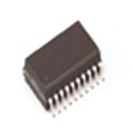
ICGOO电子元器件商城为您提供MC908JK3ECDWE由Freescale Semiconductor设计生产,在icgoo商城现货销售,并且可以通过原厂、代理商等渠道进行代购。 MC908JK3ECDWE价格参考。Freescale SemiconductorMC908JK3ECDWE封装/规格:嵌入式 - 微控制器, HC08 微控制器 IC HC08 8-位 8MHz 4KB(4K x 8) 闪存 20-SOIC。您可以下载MC908JK3ECDWE参考资料、Datasheet数据手册功能说明书,资料中有MC908JK3ECDWE 详细功能的应用电路图电压和使用方法及教程。
| 参数 | 数值 |
| A/D位大小 | 8 bit |
| 产品目录 | 集成电路 (IC)半导体 |
| 描述 | IC MCU 8BIT 4KB FLASH 20SOIC8位微控制器 -MCU MCU 128RAM 4K FLASH A/D |
| EEPROM容量 | - |
| 产品分类 | |
| I/O数 | 15 |
| 品牌 | Freescale Semiconductor |
| 产品手册 | http://cache.freescale.com/webapp/sps/site/prod_summary.jsp?code=HC08JK-JL&tab=Documentation_Tab&Type=Data+Sheets |
| 产品图片 |
|
| rohs | 符合RoHS无铅 / 符合限制有害物质指令(RoHS)规范要求 |
| 产品系列 | 嵌入式处理器和控制器,微控制器 - MCU,8位微控制器 -MCU,Freescale Semiconductor MC908JK3ECDWEHC08 |
| 数据手册 | |
| 产品型号 | MC908JK3ECDWE |
| PCN设计/规格 | http://cache.freescale.com/files/shared/doc/pcn/PCN16235.htm |
| RAM容量 | 128 x 8 |
| 产品目录页面 | |
| 产品种类 | 8位微控制器 -MCU |
| 供应商器件封装 | 20-SOIC W |
| 包装 | 管件 |
| 单位重量 | 519.500 mg |
| 可用A/D通道 | 12 |
| 可编程输入/输出端数量 | 26 |
| 商标 | Freescale Semiconductor |
| 处理器系列 | HC08JK |
| 外设 | LED,LVD,POR,PWM |
| 安装风格 | SMD/SMT |
| 定时器数量 | 2 Timer |
| 封装 | Tube |
| 封装/外壳 | 20-SOIC(0.295",7.50mm 宽) |
| 封装/箱体 | SOIC-20 |
| 工作温度 | -40°C ~ 85°C |
| 工作电源电压 | 3 V to 5 V |
| 工厂包装数量 | 38 |
| 振荡器类型 | 外部 |
| 数据RAM大小 | 128 B |
| 数据Rom类型 | Flash |
| 数据总线宽度 | 8 bit |
| 数据转换器 | A/D 12x8b |
| 最大工作温度 | + 85 C |
| 最大时钟频率 | 8 MHz |
| 最小工作温度 | - 40 C |
| 标准包装 | 1,938 |
| 核心 | HC08 |
| 核心处理器 | HC08 |
| 核心尺寸 | 8-位 |
| 片上ADC | Yes |
| 电压-电源(Vcc/Vdd) | 2.7 V ~ 3.3 V |
| 电源电压-最大 | 5.5 V |
| 电源电压-最小 | 2.7 V |
| 程序存储器大小 | 4 kB |
| 程序存储器类型 | Flash |
| 程序存储容量 | 4KB(4K x 8) |
| 系列 | HC08JK_JL |
| 输入/输出端数量 | 26 I/O |
| 连接性 | - |
| 速度 | 8MHz |


.jpg)


- 商务部:美国ITC正式对集成电路等产品启动337调查
- 曝三星4nm工艺存在良率问题 高通将骁龙8 Gen1或转产台积电
- 太阳诱电将投资9.5亿元在常州建新厂生产MLCC 预计2023年完工
- 英特尔发布欧洲新工厂建设计划 深化IDM 2.0 战略
- 台积电先进制程称霸业界 有大客户加持明年业绩稳了
- 达到5530亿美元!SIA预计今年全球半导体销售额将创下新高
- 英特尔拟将自动驾驶子公司Mobileye上市 估值或超500亿美元
- 三星加码芯片和SET,合并消费电子和移动部门,撤换高东真等 CEO
- 三星电子宣布重大人事变动 还合并消费电子和移动部门
- 海关总署:前11个月进口集成电路产品价值2.52万亿元 增长14.8%


PDF Datasheet 数据手册内容提取
MC68HC908JL3/JK3E/JK1E MC68HRC908JL3/JK3E/JK1E MC68HLC908JL3/JK3E/JK1E MC68HC903KL3E/KK3E MC68HC08JL3E/JK3E MC68HRC08JL3E/JK3E Data Sheet M68HC08 Microcontrollers MC68HC908JL3E Rev. 4 10/2006 freescale.com
None
MC68HC908JL3/JK3E/JK1E MC68HRC908JL3/JK3E/JK1E MC68HLC908JL3/JK3E/JK1E MC68HC908KL3E/KK3E MC68HC08JL3E/JK3E MC68HRC08JL3E/JK3E Data Sheet To provide the most up-to-date information, the revision of our documents on the World Wide Web will be the most current. Your printed copy may be an earlier revision. To verify you have the latest information available, refer to: http://www.freescale.com Freescale™ and the Freescale logo are trademarks of Freescale Semiconductor, Inc. This product incorporates SuperFlash® technology licensed from SST. ©Freescale Semiconductor, Inc., 2004, 2006. All rights reserved. MC68HC908JL3E Family Data Sheet, Rev. 4 Freescale Semiconductor 3
The following revision history table summarizes changes contained in this document. For your convenience, the page number designators have been linked to the appropriate location. Revision History Revision Page Date Description Level Number(s) Table 4-1. Instruction Set Summary — Updated table to include the 42 WAIT instruction. 5.7.1 Break Status Register (BSR) — Updated for clarity. 63 5.7.2 Reset Status Register (RSR) — Updated description for clarity. 64 7.4 Security — Updated to reflect the correct RAM location ($80) to 80 determine if the security code has been entered correctly. October 2006 4 8.9.1 TIM Status and Control Register (TSC) — Added note to definition 89 of TSTOP bit. 10.1 Introduction — Added note regarding 20-pin devices. 103 15.4.3 Break Status Register — Updated for clarity. 132 Chapter 17 Mechanical Specifications — Updated package drawings to 147 the latest available. Added appendix B for ROM parts. 159–166 Nov 2004 3 Added appendix C for ADC-less parts. 167–170 Added appendix A for low-volt devices. 153–224 Dec 2002 2 Updated Monitor Mode Circuit (Figure7-1) and Monitor Mode Entry 76, 77 Requirements and Options (Table7-1) in Monitor ROM section. May 2002 1 First general release. — MC68HC908JL3E Family Data Sheet, Rev. 4 4 Freescale Semiconductor
List of Chapters Chapter 1 General Description. . . . . . . . . . . . . . . . . . . . . . . . . . . . . . . . . . . . . . . . . . . . . . . .15 Chapter 2 Memory. . . . . . . . . . . . . . . . . . . . . . . . . . . . . . . . . . . . . . . . . . . . . . . . . . . . . . . . . .21 Chapter 3 Configuration Registers (CONFIG) . . . . . . . . . . . . . . . . . . . . . . . . . . . . . . . . . . .35 Chapter 4 Central Processor Unit (CPU). . . . . . . . . . . . . . . . . . . . . . . . . . . . . . . . . . . . . . . .37 Chapter 5 System Integration Module (SIM). . . . . . . . . . . . . . . . . . . . . . . . . . . . . . . . . . . . .49 Chapter 6 Oscillator (OSC). . . . . . . . . . . . . . . . . . . . . . . . . . . . . . . . . . . . . . . . . . . . . . . . . . .67 Chapter 7 Monitor ROM (MON) . . . . . . . . . . . . . . . . . . . . . . . . . . . . . . . . . . . . . . . . . . . . . . .71 Chapter 8 Timer Interface Module (TIM) . . . . . . . . . . . . . . . . . . . . . . . . . . . . . . . . . . . . . . . .81 Chapter 9 Analog-to-Digital Converter (ADC). . . . . . . . . . . . . . . . . . . . . . . . . . . . . . . . . . . .97 Chapter 10 Input/Output (I/O) Ports. . . . . . . . . . . . . . . . . . . . . . . . . . . . . . . . . . . . . . . . . . .103 Chapter 11 External Interrupt (IRQ). . . . . . . . . . . . . . . . . . . . . . . . . . . . . . . . . . . . . . . . . . .113 Chapter 12 Keyboard Interrupt Module (KBI). . . . . . . . . . . . . . . . . . . . . . . . . . . . . . . . . . .117 Chapter 13 Computer Operating Properly (COP). . . . . . . . . . . . . . . . . . . . . . . . . . . . . . . .123 Chapter 14 Low Voltage Inhibit (LVI). . . . . . . . . . . . . . . . . . . . . . . . . . . . . . . . . . . . . . . . . .127 Chapter 15 Break Module (BREAK). . . . . . . . . . . . . . . . . . . . . . . . . . . . . . . . . . . . . . . . . . .129 Chapter 16 Electrical Specifications. . . . . . . . . . . . . . . . . . . . . . . . . . . . . . . . . . . . . . . . . .135 Chapter 17 Mechanical Specifications . . . . . . . . . . . . . . . . . . . . . . . . . . . . . . . . . . . . . . . .147 Chapter 18 Ordering Information. . . . . . . . . . . . . . . . . . . . . . . . . . . . . . . . . . . . . . . . . . . . .157 Appendix A MC68HLC908JL3E/JK3E/JK1E . . . . . . . . . . . . . . . . . . . . . . . . . . . . . . . . . . . .159 Appendix B MC68H(R)C08JL3E/JK3E. . . . . . . . . . . . . . . . . . . . . . . . . . . . . . . . . . . . . . . . .165 Appendix C MC68HC908KL3E/KK3E. . . . . . . . . . . . . . . . . . . . . . . . . . . . . . . . . . . . . . . . . .175 MC68HC908JL3E Family Data Sheet, Rev. 4 Freescale Semiconductor 5
List of Chapters MC68HC908JL3E Family Data Sheet, Rev. 4 6 Freescale Semiconductor
Table of Contents Chapter 1 General Description 1.1 Introduction . . . . . . . . . . . . . . . . . . . . . . . . . . . . . . . . . . . . . . . . . . . . . . . . . . . . . . . . . . . . . . . . 15 1.2 Features. . . . . . . . . . . . . . . . . . . . . . . . . . . . . . . . . . . . . . . . . . . . . . . . . . . . . . . . . . . . . . . . . . . 16 1.3 MCU Block Diagram . . . . . . . . . . . . . . . . . . . . . . . . . . . . . . . . . . . . . . . . . . . . . . . . . . . . . . . . . 17 1.4 Pin Assignments . . . . . . . . . . . . . . . . . . . . . . . . . . . . . . . . . . . . . . . . . . . . . . . . . . . . . . . . . . . . 18 1.5 Pin Functions. . . . . . . . . . . . . . . . . . . . . . . . . . . . . . . . . . . . . . . . . . . . . . . . . . . . . . . . . . . . . . . 20 Chapter 2 Memory 2.1 Introduction . . . . . . . . . . . . . . . . . . . . . . . . . . . . . . . . . . . . . . . . . . . . . . . . . . . . . . . . . . . . . . . . 21 2.2 I/O Section. . . . . . . . . . . . . . . . . . . . . . . . . . . . . . . . . . . . . . . . . . . . . . . . . . . . . . . . . . . . . . . . . 21 2.3 Monitor ROM . . . . . . . . . . . . . . . . . . . . . . . . . . . . . . . . . . . . . . . . . . . . . . . . . . . . . . . . . . . . . . . 21 2.4 Random-Access Memory (RAM). . . . . . . . . . . . . . . . . . . . . . . . . . . . . . . . . . . . . . . . . . . . . . . . 27 2.5 Flash Memory . . . . . . . . . . . . . . . . . . . . . . . . . . . . . . . . . . . . . . . . . . . . . . . . . . . . . . . . . . . . . . 28 2.6 Functional Description. . . . . . . . . . . . . . . . . . . . . . . . . . . . . . . . . . . . . . . . . . . . . . . . . . . . . . . . 28 2.7 Flash Control Register. . . . . . . . . . . . . . . . . . . . . . . . . . . . . . . . . . . . . . . . . . . . . . . . . . . . . . . . 29 2.8 Flash Page Erase Operation . . . . . . . . . . . . . . . . . . . . . . . . . . . . . . . . . . . . . . . . . . . . . . . . . . . 30 2.9 Flash Mass Erase Operation. . . . . . . . . . . . . . . . . . . . . . . . . . . . . . . . . . . . . . . . . . . . . . . . . . . 30 2.10 Flash Program Operation. . . . . . . . . . . . . . . . . . . . . . . . . . . . . . . . . . . . . . . . . . . . . . . . . . . . . . 31 2.11 Flash Protection. . . . . . . . . . . . . . . . . . . . . . . . . . . . . . . . . . . . . . . . . . . . . . . . . . . . . . . . . . . . . 31 2.12 Flash Block Protect Register . . . . . . . . . . . . . . . . . . . . . . . . . . . . . . . . . . . . . . . . . . . . . . . . . . . 33 Chapter 3 Configuration Registers (CONFIG) 3.1 Introduction . . . . . . . . . . . . . . . . . . . . . . . . . . . . . . . . . . . . . . . . . . . . . . . . . . . . . . . . . . . . . . . . 35 3.2 Functional Description. . . . . . . . . . . . . . . . . . . . . . . . . . . . . . . . . . . . . . . . . . . . . . . . . . . . . . . . 35 3.3 Configuration Register 1 (CONFIG1). . . . . . . . . . . . . . . . . . . . . . . . . . . . . . . . . . . . . . . . . . . . . 35 3.4 Configuration Register 2 (CONFIG2). . . . . . . . . . . . . . . . . . . . . . . . . . . . . . . . . . . . . . . . . . . . . 36 Chapter 4 Central Processor Unit (CPU) 4.1 Introduction . . . . . . . . . . . . . . . . . . . . . . . . . . . . . . . . . . . . . . . . . . . . . . . . . . . . . . . . . . . . . . . . 37 4.2 Features. . . . . . . . . . . . . . . . . . . . . . . . . . . . . . . . . . . . . . . . . . . . . . . . . . . . . . . . . . . . . . . . . . . 37 4.3 CPU Registers. . . . . . . . . . . . . . . . . . . . . . . . . . . . . . . . . . . . . . . . . . . . . . . . . . . . . . . . . . . . . . 37 4.3.1 Accumulator. . . . . . . . . . . . . . . . . . . . . . . . . . . . . . . . . . . . . . . . . . . . . . . . . . . . . . . . . . . . . 38 4.3.2 Index Register . . . . . . . . . . . . . . . . . . . . . . . . . . . . . . . . . . . . . . . . . . . . . . . . . . . . . . . . . . . 38 4.3.3 Stack Pointer . . . . . . . . . . . . . . . . . . . . . . . . . . . . . . . . . . . . . . . . . . . . . . . . . . . . . . . . . . . . 39 MC68HC908JL3E Family Data Sheet, Rev. 4 Freescale Semiconductor 7
Table of Contents 4.3.4 Program Counter . . . . . . . . . . . . . . . . . . . . . . . . . . . . . . . . . . . . . . . . . . . . . . . . . . . . . . . . . 39 4.3.5 Condition Code Register . . . . . . . . . . . . . . . . . . . . . . . . . . . . . . . . . . . . . . . . . . . . . . . . . . . 40 4.4 Arithmetic/Logic Unit (ALU) . . . . . . . . . . . . . . . . . . . . . . . . . . . . . . . . . . . . . . . . . . . . . . . . . . . . 41 4.5 Low-Power Modes. . . . . . . . . . . . . . . . . . . . . . . . . . . . . . . . . . . . . . . . . . . . . . . . . . . . . . . . . . . 41 4.5.1 Wait Mode . . . . . . . . . . . . . . . . . . . . . . . . . . . . . . . . . . . . . . . . . . . . . . . . . . . . . . . . . . . . . . 41 4.5.2 Stop Mode . . . . . . . . . . . . . . . . . . . . . . . . . . . . . . . . . . . . . . . . . . . . . . . . . . . . . . . . . . . . . . 41 4.6 CPU During Break Interrupts. . . . . . . . . . . . . . . . . . . . . . . . . . . . . . . . . . . . . . . . . . . . . . . . . . . 41 4.7 Instruction Set Summary . . . . . . . . . . . . . . . . . . . . . . . . . . . . . . . . . . . . . . . . . . . . . . . . . . . . . . 42 4.8 Opcode Map . . . . . . . . . . . . . . . . . . . . . . . . . . . . . . . . . . . . . . . . . . . . . . . . . . . . . . . . . . . . . . . 47 Chapter 5 System Integration Module (SIM) 5.1 Introduction . . . . . . . . . . . . . . . . . . . . . . . . . . . . . . . . . . . . . . . . . . . . . . . . . . . . . . . . . . . . . . . . 49 5.2 SIM Bus Clock Control and Generation. . . . . . . . . . . . . . . . . . . . . . . . . . . . . . . . . . . . . . . . . . . 51 5.2.1 Bus Timing. . . . . . . . . . . . . . . . . . . . . . . . . . . . . . . . . . . . . . . . . . . . . . . . . . . . . . . . . . . . . . 51 5.2.2 Clock Start-Up from POR. . . . . . . . . . . . . . . . . . . . . . . . . . . . . . . . . . . . . . . . . . . . . . . . . . . 51 5.2.3 Clocks in Stop Mode and Wait Mode. . . . . . . . . . . . . . . . . . . . . . . . . . . . . . . . . . . . . . . . . . 51 5.3 Reset and System Initialization . . . . . . . . . . . . . . . . . . . . . . . . . . . . . . . . . . . . . . . . . . . . . . . . . 52 5.3.1 External Pin Reset. . . . . . . . . . . . . . . . . . . . . . . . . . . . . . . . . . . . . . . . . . . . . . . . . . . . . . . . 52 5.3.2 Active Resets from Internal Sources . . . . . . . . . . . . . . . . . . . . . . . . . . . . . . . . . . . . . . . . . . 52 5.3.2.1 Power-On Reset. . . . . . . . . . . . . . . . . . . . . . . . . . . . . . . . . . . . . . . . . . . . . . . . . . . . . . . . 53 5.3.2.2 Computer Operating Properly (COP) Reset. . . . . . . . . . . . . . . . . . . . . . . . . . . . . . . . . . . 54 5.3.2.3 Illegal Opcode Reset . . . . . . . . . . . . . . . . . . . . . . . . . . . . . . . . . . . . . . . . . . . . . . . . . . . . 54 5.3.2.4 Illegal Address Reset . . . . . . . . . . . . . . . . . . . . . . . . . . . . . . . . . . . . . . . . . . . . . . . . . . . . 54 5.3.2.5 LVI Reset . . . . . . . . . . . . . . . . . . . . . . . . . . . . . . . . . . . . . . . . . . . . . . . . . . . . . . . . . . . . . 55 5.4 SIM Counter. . . . . . . . . . . . . . . . . . . . . . . . . . . . . . . . . . . . . . . . . . . . . . . . . . . . . . . . . . . . . . . . 55 5.4.1 SIM Counter During Power-On Reset . . . . . . . . . . . . . . . . . . . . . . . . . . . . . . . . . . . . . . . . . 55 5.4.2 SIM Counter During Stop Mode Recovery. . . . . . . . . . . . . . . . . . . . . . . . . . . . . . . . . . . . . . 55 5.4.3 SIM Counter and Reset States . . . . . . . . . . . . . . . . . . . . . . . . . . . . . . . . . . . . . . . . . . . . . . 55 5.5 Exception Control. . . . . . . . . . . . . . . . . . . . . . . . . . . . . . . . . . . . . . . . . . . . . . . . . . . . . . . . . . . . 55 5.5.1 Interrupts . . . . . . . . . . . . . . . . . . . . . . . . . . . . . . . . . . . . . . . . . . . . . . . . . . . . . . . . . . . . . . . 55 5.5.1.1 Hardware Interrupts . . . . . . . . . . . . . . . . . . . . . . . . . . . . . . . . . . . . . . . . . . . . . . . . . . . . . 57 5.5.1.2 SWI Instruction. . . . . . . . . . . . . . . . . . . . . . . . . . . . . . . . . . . . . . . . . . . . . . . . . . . . . . . . . 58 5.5.2 Interrupt Status Registers . . . . . . . . . . . . . . . . . . . . . . . . . . . . . . . . . . . . . . . . . . . . . . . . . . 58 5.5.2.1 Interrupt Status Register 1 . . . . . . . . . . . . . . . . . . . . . . . . . . . . . . . . . . . . . . . . . . . . . . . . 59 5.5.2.2 Interrupt Status Register 2 . . . . . . . . . . . . . . . . . . . . . . . . . . . . . . . . . . . . . . . . . . . . . . . . 59 5.5.2.3 Interrupt Status Register 3 . . . . . . . . . . . . . . . . . . . . . . . . . . . . . . . . . . . . . . . . . . . . . . . . 60 5.5.3 Reset . . . . . . . . . . . . . . . . . . . . . . . . . . . . . . . . . . . . . . . . . . . . . . . . . . . . . . . . . . . . . . . . . . 60 5.5.4 Break Interrupts . . . . . . . . . . . . . . . . . . . . . . . . . . . . . . . . . . . . . . . . . . . . . . . . . . . . . . . . . . 60 5.5.5 Status Flag Protection in Break Mode . . . . . . . . . . . . . . . . . . . . . . . . . . . . . . . . . . . . . . . . . 60 5.6 Low-Power Modes. . . . . . . . . . . . . . . . . . . . . . . . . . . . . . . . . . . . . . . . . . . . . . . . . . . . . . . . . . . 61 5.6.1 Wait Mode . . . . . . . . . . . . . . . . . . . . . . . . . . . . . . . . . . . . . . . . . . . . . . . . . . . . . . . . . . . . . . 61 5.6.2 Stop Mode . . . . . . . . . . . . . . . . . . . . . . . . . . . . . . . . . . . . . . . . . . . . . . . . . . . . . . . . . . . . . . 62 5.7 SIM Registers . . . . . . . . . . . . . . . . . . . . . . . . . . . . . . . . . . . . . . . . . . . . . . . . . . . . . . . . . . . . . . 63 5.7.1 Break Status Register (BSR). . . . . . . . . . . . . . . . . . . . . . . . . . . . . . . . . . . . . . . . . . . . . . . . 63 5.7.2 Reset Status Register (RSR). . . . . . . . . . . . . . . . . . . . . . . . . . . . . . . . . . . . . . . . . . . . . . . . 64 5.7.3 Break Flag Control Register (BFCR) . . . . . . . . . . . . . . . . . . . . . . . . . . . . . . . . . . . . . . . . . . 65 MC68HC908JL3E Family Data Sheet, Rev. 4 8 Freescale Semiconductor
Chapter 6 Oscillator (OSC) 6.1 Introduction . . . . . . . . . . . . . . . . . . . . . . . . . . . . . . . . . . . . . . . . . . . . . . . . . . . . . . . . . . . . . . . . 67 6.2 X-tal Oscillator (MC68HC908JL3E/JK3E/JK1E) . . . . . . . . . . . . . . . . . . . . . . . . . . . . . . . . . . . . 67 6.3 RC Oscillator (MC68HRC908JL3E/JK3E/JK1E) . . . . . . . . . . . . . . . . . . . . . . . . . . . . . . . . . . . . 67 6.4 I/O Signals. . . . . . . . . . . . . . . . . . . . . . . . . . . . . . . . . . . . . . . . . . . . . . . . . . . . . . . . . . . . . . . . . 69 6.4.1 Crystal Amplifier Input Pin (OSC1). . . . . . . . . . . . . . . . . . . . . . . . . . . . . . . . . . . . . . . . . . . . 69 6.4.2 Crystal Amplifier Output Pin (OSC2/PTA6/RCCLK). . . . . . . . . . . . . . . . . . . . . . . . . . . . . . . 69 6.4.3 Oscillator Enable Signal (SIMOSCEN) . . . . . . . . . . . . . . . . . . . . . . . . . . . . . . . . . . . . . . . . 69 6.4.4 X-tal Oscillator Clock (XTALCLK) . . . . . . . . . . . . . . . . . . . . . . . . . . . . . . . . . . . . . . . . . . . . 69 6.4.5 RC Oscillator Clock (RCCLK) . . . . . . . . . . . . . . . . . . . . . . . . . . . . . . . . . . . . . . . . . . . . . . . 69 6.4.6 Oscillator Out 2 (2OSCOUT) . . . . . . . . . . . . . . . . . . . . . . . . . . . . . . . . . . . . . . . . . . . . . . . . 69 6.4.7 Oscillator Out (OSCOUT). . . . . . . . . . . . . . . . . . . . . . . . . . . . . . . . . . . . . . . . . . . . . . . . . . . 69 6.5 Low Power Modes. . . . . . . . . . . . . . . . . . . . . . . . . . . . . . . . . . . . . . . . . . . . . . . . . . . . . . . . . . . 70 6.5.1 Wait Mode . . . . . . . . . . . . . . . . . . . . . . . . . . . . . . . . . . . . . . . . . . . . . . . . . . . . . . . . . . . . . . 70 6.5.2 Stop Mode . . . . . . . . . . . . . . . . . . . . . . . . . . . . . . . . . . . . . . . . . . . . . . . . . . . . . . . . . . . . . . 70 6.6 Oscillator During Break Mode . . . . . . . . . . . . . . . . . . . . . . . . . . . . . . . . . . . . . . . . . . . . . . . . . . 70 Chapter 7 Monitor ROM (MON) 7.1 Introduction . . . . . . . . . . . . . . . . . . . . . . . . . . . . . . . . . . . . . . . . . . . . . . . . . . . . . . . . . . . . . . . . 71 7.2 Features. . . . . . . . . . . . . . . . . . . . . . . . . . . . . . . . . . . . . . . . . . . . . . . . . . . . . . . . . . . . . . . . . . . 71 7.3 Functional Description. . . . . . . . . . . . . . . . . . . . . . . . . . . . . . . . . . . . . . . . . . . . . . . . . . . . . . . . 71 7.3.1 Entering Monitor Mode. . . . . . . . . . . . . . . . . . . . . . . . . . . . . . . . . . . . . . . . . . . . . . . . . . . . . 73 7.3.2 Baud Rate . . . . . . . . . . . . . . . . . . . . . . . . . . . . . . . . . . . . . . . . . . . . . . . . . . . . . . . . . . . . . . 75 7.3.3 Data Format. . . . . . . . . . . . . . . . . . . . . . . . . . . . . . . . . . . . . . . . . . . . . . . . . . . . . . . . . . . . . 76 7.3.4 Echoing . . . . . . . . . . . . . . . . . . . . . . . . . . . . . . . . . . . . . . . . . . . . . . . . . . . . . . . . . . . . . . . . 76 7.3.5 Break Signal. . . . . . . . . . . . . . . . . . . . . . . . . . . . . . . . . . . . . . . . . . . . . . . . . . . . . . . . . . . . . 76 7.3.6 Commands. . . . . . . . . . . . . . . . . . . . . . . . . . . . . . . . . . . . . . . . . . . . . . . . . . . . . . . . . . . . . . 77 7.4 Security . . . . . . . . . . . . . . . . . . . . . . . . . . . . . . . . . . . . . . . . . . . . . . . . . . . . . . . . . . . . . . . . . . . 79 Chapter 8 Timer Interface Module (TIM) 8.1 Introduction . . . . . . . . . . . . . . . . . . . . . . . . . . . . . . . . . . . . . . . . . . . . . . . . . . . . . . . . . . . . . . . . 81 8.2 Features. . . . . . . . . . . . . . . . . . . . . . . . . . . . . . . . . . . . . . . . . . . . . . . . . . . . . . . . . . . . . . . . . . . 81 8.3 Pin Name Conventions . . . . . . . . . . . . . . . . . . . . . . . . . . . . . . . . . . . . . . . . . . . . . . . . . . . . . . . 81 8.4 Functional Description. . . . . . . . . . . . . . . . . . . . . . . . . . . . . . . . . . . . . . . . . . . . . . . . . . . . . . . . 82 8.4.1 TIM Counter Prescaler. . . . . . . . . . . . . . . . . . . . . . . . . . . . . . . . . . . . . . . . . . . . . . . . . . . . . 84 8.4.2 Input Capture. . . . . . . . . . . . . . . . . . . . . . . . . . . . . . . . . . . . . . . . . . . . . . . . . . . . . . . . . . . . 84 8.4.3 Output Compare. . . . . . . . . . . . . . . . . . . . . . . . . . . . . . . . . . . . . . . . . . . . . . . . . . . . . . . . . . 84 8.4.3.1 Unbuffered Output Compare . . . . . . . . . . . . . . . . . . . . . . . . . . . . . . . . . . . . . . . . . . . . . . 84 8.4.3.2 Buffered Output Compare . . . . . . . . . . . . . . . . . . . . . . . . . . . . . . . . . . . . . . . . . . . . . . . . 84 8.4.4 Pulse Width Modulation (PWM). . . . . . . . . . . . . . . . . . . . . . . . . . . . . . . . . . . . . . . . . . . . . . 85 8.4.4.1 Unbuffered PWM Signal Generation . . . . . . . . . . . . . . . . . . . . . . . . . . . . . . . . . . . . . . . . 86 8.4.4.2 Buffered PWM Signal Generation . . . . . . . . . . . . . . . . . . . . . . . . . . . . . . . . . . . . . . . . . . 86 8.4.4.3 PWM Initialization. . . . . . . . . . . . . . . . . . . . . . . . . . . . . . . . . . . . . . . . . . . . . . . . . . . . . . . 87 MC68HC908JL3E Family Data Sheet, Rev. 4 Freescale Semiconductor 9
Table of Contents 8.5 Interrupts . . . . . . . . . . . . . . . . . . . . . . . . . . . . . . . . . . . . . . . . . . . . . . . . . . . . . . . . . . . . . . . . . . 88 8.6 Low-Power Modes. . . . . . . . . . . . . . . . . . . . . . . . . . . . . . . . . . . . . . . . . . . . . . . . . . . . . . . . . . . 88 8.6.1 Wait Mode . . . . . . . . . . . . . . . . . . . . . . . . . . . . . . . . . . . . . . . . . . . . . . . . . . . . . . . . . . . . . . 88 8.6.2 Stop Mode . . . . . . . . . . . . . . . . . . . . . . . . . . . . . . . . . . . . . . . . . . . . . . . . . . . . . . . . . . . . . . 88 8.7 TIM During Break Interrupts. . . . . . . . . . . . . . . . . . . . . . . . . . . . . . . . . . . . . . . . . . . . . . . . . . . . 88 8.8 I/O Signals. . . . . . . . . . . . . . . . . . . . . . . . . . . . . . . . . . . . . . . . . . . . . . . . . . . . . . . . . . . . . . . . . 89 8.9 I/O Registers . . . . . . . . . . . . . . . . . . . . . . . . . . . . . . . . . . . . . . . . . . . . . . . . . . . . . . . . . . . . . . . 89 8.9.1 TIM Status and Control Register (TSC). . . . . . . . . . . . . . . . . . . . . . . . . . . . . . . . . . . . . . . . 89 8.9.2 TIM Counter Registers (TCNTH:TCNTL). . . . . . . . . . . . . . . . . . . . . . . . . . . . . . . . . . . . . . . 91 8.9.3 TIM Counter Modulo Registers (TMODH:TMODL) . . . . . . . . . . . . . . . . . . . . . . . . . . . . . . . 91 8.9.4 TIM Channel Status and Control Registers (TSC0:TSC1). . . . . . . . . . . . . . . . . . . . . . . . . . 92 8.9.5 TIM Channel Registers (TCH0H/L:TCH1H/L) . . . . . . . . . . . . . . . . . . . . . . . . . . . . . . . . . . . 95 Chapter 9 Analog-to-Digital Converter (ADC) 9.1 Introduction . . . . . . . . . . . . . . . . . . . . . . . . . . . . . . . . . . . . . . . . . . . . . . . . . . . . . . . . . . . . . . . . 97 9.2 Features. . . . . . . . . . . . . . . . . . . . . . . . . . . . . . . . . . . . . . . . . . . . . . . . . . . . . . . . . . . . . . . . . . . 97 9.3 Functional Description. . . . . . . . . . . . . . . . . . . . . . . . . . . . . . . . . . . . . . . . . . . . . . . . . . . . . . . . 97 9.3.1 ADC Port I/O Pins . . . . . . . . . . . . . . . . . . . . . . . . . . . . . . . . . . . . . . . . . . . . . . . . . . . . . . . . 98 9.3.2 Voltage Conversion . . . . . . . . . . . . . . . . . . . . . . . . . . . . . . . . . . . . . . . . . . . . . . . . . . . . . . . 99 9.3.3 Conversion Time . . . . . . . . . . . . . . . . . . . . . . . . . . . . . . . . . . . . . . . . . . . . . . . . . . . . . . . . . 99 9.3.4 Continuous Conversion . . . . . . . . . . . . . . . . . . . . . . . . . . . . . . . . . . . . . . . . . . . . . . . . . . . . 99 9.3.5 Accuracy and Precision . . . . . . . . . . . . . . . . . . . . . . . . . . . . . . . . . . . . . . . . . . . . . . . . . . . . 99 9.4 Interrupts . . . . . . . . . . . . . . . . . . . . . . . . . . . . . . . . . . . . . . . . . . . . . . . . . . . . . . . . . . . . . . . . . . 99 9.5 Low-Power Modes. . . . . . . . . . . . . . . . . . . . . . . . . . . . . . . . . . . . . . . . . . . . . . . . . . . . . . . . . . . 99 9.5.1 Wait Mode . . . . . . . . . . . . . . . . . . . . . . . . . . . . . . . . . . . . . . . . . . . . . . . . . . . . . . . . . . . . . . 99 9.5.2 Stop Mode . . . . . . . . . . . . . . . . . . . . . . . . . . . . . . . . . . . . . . . . . . . . . . . . . . . . . . . . . . . . . 100 9.6 I/O Signals. . . . . . . . . . . . . . . . . . . . . . . . . . . . . . . . . . . . . . . . . . . . . . . . . . . . . . . . . . . . . . . . 100 9.6.1 ADC Voltage In (ADCVIN). . . . . . . . . . . . . . . . . . . . . . . . . . . . . . . . . . . . . . . . . . . . . . . . . 100 9.7 I/O Registers . . . . . . . . . . . . . . . . . . . . . . . . . . . . . . . . . . . . . . . . . . . . . . . . . . . . . . . . . . . . . . 100 9.7.1 ADC Status and Control Register . . . . . . . . . . . . . . . . . . . . . . . . . . . . . . . . . . . . . . . . . . . 100 9.7.2 ADC Data Register. . . . . . . . . . . . . . . . . . . . . . . . . . . . . . . . . . . . . . . . . . . . . . . . . . . . . . . 102 9.7.3 ADC Input Clock Register . . . . . . . . . . . . . . . . . . . . . . . . . . . . . . . . . . . . . . . . . . . . . . . . . 102 Chapter 10 Input/Output (I/O) Ports 10.1 Introduction . . . . . . . . . . . . . . . . . . . . . . . . . . . . . . . . . . . . . . . . . . . . . . . . . . . . . . . . . . . . . . . 103 10.2 Port A. . . . . . . . . . . . . . . . . . . . . . . . . . . . . . . . . . . . . . . . . . . . . . . . . . . . . . . . . . . . . . . . . . . . 105 10.2.1 Port A Data Register (PTA) . . . . . . . . . . . . . . . . . . . . . . . . . . . . . . . . . . . . . . . . . . . . . . . . 105 10.2.2 Data Direction Register A (DDRA). . . . . . . . . . . . . . . . . . . . . . . . . . . . . . . . . . . . . . . . . . . 106 10.2.3 Port A Input Pull-up Enable Register (PTAPUE) . . . . . . . . . . . . . . . . . . . . . . . . . . . . . . . . 107 10.3 Port B. . . . . . . . . . . . . . . . . . . . . . . . . . . . . . . . . . . . . . . . . . . . . . . . . . . . . . . . . . . . . . . . . . . . 108 10.3.1 Port B Data Register (PTB) . . . . . . . . . . . . . . . . . . . . . . . . . . . . . . . . . . . . . . . . . . . . . . . . 108 10.3.2 Data Direction Register B (DDRB). . . . . . . . . . . . . . . . . . . . . . . . . . . . . . . . . . . . . . . . . . . 108 MC68HC908JL3E Family Data Sheet, Rev. 4 10 Freescale Semiconductor
10.4 Port D. . . . . . . . . . . . . . . . . . . . . . . . . . . . . . . . . . . . . . . . . . . . . . . . . . . . . . . . . . . . . . . . . . . . 110 10.4.1 Port D Data Register (PTD). . . . . . . . . . . . . . . . . . . . . . . . . . . . . . . . . . . . . . . . . . . . . . . . 110 10.4.2 Data Direction Register D (DDRD). . . . . . . . . . . . . . . . . . . . . . . . . . . . . . . . . . . . . . . . . . . 111 10.4.3 Port D Control Register (PDCR) . . . . . . . . . . . . . . . . . . . . . . . . . . . . . . . . . . . . . . . . . . . . 112 Chapter 11 External Interrupt (IRQ) 11.1 Introduction . . . . . . . . . . . . . . . . . . . . . . . . . . . . . . . . . . . . . . . . . . . . . . . . . . . . . . . . . . . . . . . 113 11.2 Features. . . . . . . . . . . . . . . . . . . . . . . . . . . . . . . . . . . . . . . . . . . . . . . . . . . . . . . . . . . . . . . . . . 113 11.3 Functional Description. . . . . . . . . . . . . . . . . . . . . . . . . . . . . . . . . . . . . . . . . . . . . . . . . . . . . . . 113 11.3.1 IRQ Pin. . . . . . . . . . . . . . . . . . . . . . . . . . . . . . . . . . . . . . . . . . . . . . . . . . . . . . . . . . . . . . . . 115 11.4 IRQ Module During Break Interrupts . . . . . . . . . . . . . . . . . . . . . . . . . . . . . . . . . . . . . . . . . . . . 115 11.5 IRQ Status and Control Register (INTSCR). . . . . . . . . . . . . . . . . . . . . . . . . . . . . . . . . . . . . . . 116 Chapter 12 Keyboard Interrupt Module (KBI) 12.1 Introduction . . . . . . . . . . . . . . . . . . . . . . . . . . . . . . . . . . . . . . . . . . . . . . . . . . . . . . . . . . . . . . . 117 12.2 Features. . . . . . . . . . . . . . . . . . . . . . . . . . . . . . . . . . . . . . . . . . . . . . . . . . . . . . . . . . . . . . . . . . 117 12.3 I/O Pins . . . . . . . . . . . . . . . . . . . . . . . . . . . . . . . . . . . . . . . . . . . . . . . . . . . . . . . . . . . . . . . . . . 117 12.4 Functional Description. . . . . . . . . . . . . . . . . . . . . . . . . . . . . . . . . . . . . . . . . . . . . . . . . . . . . . . 118 12.4.1 Keyboard Initialization . . . . . . . . . . . . . . . . . . . . . . . . . . . . . . . . . . . . . . . . . . . . . . . . . . . . 119 12.5 Keyboard Interrupt Registers. . . . . . . . . . . . . . . . . . . . . . . . . . . . . . . . . . . . . . . . . . . . . . . . . . 119 12.5.1 Keyboard Status and Control Register. . . . . . . . . . . . . . . . . . . . . . . . . . . . . . . . . . . . . . . . 120 12.5.2 Keyboard Interrupt Enable Register. . . . . . . . . . . . . . . . . . . . . . . . . . . . . . . . . . . . . . . . . . 121 12.6 Low-Power Modes. . . . . . . . . . . . . . . . . . . . . . . . . . . . . . . . . . . . . . . . . . . . . . . . . . . . . . . . . . 121 12.6.1 Wait Mode . . . . . . . . . . . . . . . . . . . . . . . . . . . . . . . . . . . . . . . . . . . . . . . . . . . . . . . . . . . . . 121 12.6.2 Stop Mode . . . . . . . . . . . . . . . . . . . . . . . . . . . . . . . . . . . . . . . . . . . . . . . . . . . . . . . . . . . . . 121 12.7 Keyboard Module During Break Interrupts. . . . . . . . . . . . . . . . . . . . . . . . . . . . . . . . . . . . . . . . 121 Chapter 13 Computer Operating Properly (COP) 13.1 Introduction . . . . . . . . . . . . . . . . . . . . . . . . . . . . . . . . . . . . . . . . . . . . . . . . . . . . . . . . . . . . . . . 123 13.2 Functional Description. . . . . . . . . . . . . . . . . . . . . . . . . . . . . . . . . . . . . . . . . . . . . . . . . . . . . . . 123 13.3 I/O Signals. . . . . . . . . . . . . . . . . . . . . . . . . . . . . . . . . . . . . . . . . . . . . . . . . . . . . . . . . . . . . . . . 124 13.3.1 2OSCOUT . . . . . . . . . . . . . . . . . . . . . . . . . . . . . . . . . . . . . . . . . . . . . . . . . . . . . . . . . . . . . 124 13.3.2 COPCTL Write. . . . . . . . . . . . . . . . . . . . . . . . . . . . . . . . . . . . . . . . . . . . . . . . . . . . . . . . . . 124 13.3.3 Power-On Reset. . . . . . . . . . . . . . . . . . . . . . . . . . . . . . . . . . . . . . . . . . . . . . . . . . . . . . . . . 124 13.3.4 Internal Reset. . . . . . . . . . . . . . . . . . . . . . . . . . . . . . . . . . . . . . . . . . . . . . . . . . . . . . . . . . . 124 13.3.5 Reset Vector Fetch . . . . . . . . . . . . . . . . . . . . . . . . . . . . . . . . . . . . . . . . . . . . . . . . . . . . . . 124 13.3.6 COPD (COP Disable). . . . . . . . . . . . . . . . . . . . . . . . . . . . . . . . . . . . . . . . . . . . . . . . . . . . . 124 13.3.7 COPRS (COP Rate Select) . . . . . . . . . . . . . . . . . . . . . . . . . . . . . . . . . . . . . . . . . . . . . . . . 125 13.4 COP Control Register . . . . . . . . . . . . . . . . . . . . . . . . . . . . . . . . . . . . . . . . . . . . . . . . . . . . . . . 125 13.5 Interrupts . . . . . . . . . . . . . . . . . . . . . . . . . . . . . . . . . . . . . . . . . . . . . . . . . . . . . . . . . . . . . . . . . 125 13.6 Monitor Mode. . . . . . . . . . . . . . . . . . . . . . . . . . . . . . . . . . . . . . . . . . . . . . . . . . . . . . . . . . . . . . 125 13.7 Low-Power Modes. . . . . . . . . . . . . . . . . . . . . . . . . . . . . . . . . . . . . . . . . . . . . . . . . . . . . . . . . . 125 MC68HC908JL3E Family Data Sheet, Rev. 4 Freescale Semiconductor 11
Table of Contents 13.7.1 Wait Mode . . . . . . . . . . . . . . . . . . . . . . . . . . . . . . . . . . . . . . . . . . . . . . . . . . . . . . . . . . . . . 126 13.7.2 Stop Mode . . . . . . . . . . . . . . . . . . . . . . . . . . . . . . . . . . . . . . . . . . . . . . . . . . . . . . . . . . . . . 126 13.8 COP Module During Break Mode . . . . . . . . . . . . . . . . . . . . . . . . . . . . . . . . . . . . . . . . . . . . . . 126 Chapter 14 Low Voltage Inhibit (LVI) 14.1 Introduction . . . . . . . . . . . . . . . . . . . . . . . . . . . . . . . . . . . . . . . . . . . . . . . . . . . . . . . . . . . . . . . 127 14.2 Features. . . . . . . . . . . . . . . . . . . . . . . . . . . . . . . . . . . . . . . . . . . . . . . . . . . . . . . . . . . . . . . . . . 127 14.3 Functional Description. . . . . . . . . . . . . . . . . . . . . . . . . . . . . . . . . . . . . . . . . . . . . . . . . . . . . . . 127 14.4 LVI Control Register (CONFIG2/CONFIG1) . . . . . . . . . . . . . . . . . . . . . . . . . . . . . . . . . . . . . . 128 14.5 Low-Power Modes. . . . . . . . . . . . . . . . . . . . . . . . . . . . . . . . . . . . . . . . . . . . . . . . . . . . . . . . . . 128 14.5.1 Wait Mode . . . . . . . . . . . . . . . . . . . . . . . . . . . . . . . . . . . . . . . . . . . . . . . . . . . . . . . . . . . . . 128 14.5.2 Stop Mode . . . . . . . . . . . . . . . . . . . . . . . . . . . . . . . . . . . . . . . . . . . . . . . . . . . . . . . . . . . . . 128 Chapter 15 Break Module (BREAK) 15.1 Introduction . . . . . . . . . . . . . . . . . . . . . . . . . . . . . . . . . . . . . . . . . . . . . . . . . . . . . . . . . . . . . . . 129 15.2 Features. . . . . . . . . . . . . . . . . . . . . . . . . . . . . . . . . . . . . . . . . . . . . . . . . . . . . . . . . . . . . . . . . . 129 15.3 Functional Description. . . . . . . . . . . . . . . . . . . . . . . . . . . . . . . . . . . . . . . . . . . . . . . . . . . . . . . 129 15.3.1 Flag Protection During Break Interrupts. . . . . . . . . . . . . . . . . . . . . . . . . . . . . . . . . . . . . . . 130 15.3.2 CPU During Break Interrupts. . . . . . . . . . . . . . . . . . . . . . . . . . . . . . . . . . . . . . . . . . . . . . . 130 15.3.3 TIM During Break Interrupts. . . . . . . . . . . . . . . . . . . . . . . . . . . . . . . . . . . . . . . . . . . . . . . . 130 15.3.4 COP During Break Interrupts. . . . . . . . . . . . . . . . . . . . . . . . . . . . . . . . . . . . . . . . . . . . . . . 130 15.4 Break Module Registers. . . . . . . . . . . . . . . . . . . . . . . . . . . . . . . . . . . . . . . . . . . . . . . . . . . . . . 131 15.4.1 Break Status and Control Register (BRKSCR) . . . . . . . . . . . . . . . . . . . . . . . . . . . . . . . . . 131 15.4.2 Break Address Registers. . . . . . . . . . . . . . . . . . . . . . . . . . . . . . . . . . . . . . . . . . . . . . . . . . 132 15.4.3 Break Status Register . . . . . . . . . . . . . . . . . . . . . . . . . . . . . . . . . . . . . . . . . . . . . . . . . . . . 132 15.4.4 Break Flag Control Register (BFCR) . . . . . . . . . . . . . . . . . . . . . . . . . . . . . . . . . . . . . . . . . 133 15.5 Low-Power Modes. . . . . . . . . . . . . . . . . . . . . . . . . . . . . . . . . . . . . . . . . . . . . . . . . . . . . . . . . . 133 15.5.1 Wait Mode . . . . . . . . . . . . . . . . . . . . . . . . . . . . . . . . . . . . . . . . . . . . . . . . . . . . . . . . . . . . . 133 15.5.2 Stop Mode . . . . . . . . . . . . . . . . . . . . . . . . . . . . . . . . . . . . . . . . . . . . . . . . . . . . . . . . . . . . . 133 Chapter 16 Electrical Specifications 16.1 Introduction . . . . . . . . . . . . . . . . . . . . . . . . . . . . . . . . . . . . . . . . . . . . . . . . . . . . . . . . . . . . . . . 135 16.2 Absolute Maximum Ratings. . . . . . . . . . . . . . . . . . . . . . . . . . . . . . . . . . . . . . . . . . . . . . . . . . . 135 16.3 Functional Operating Range . . . . . . . . . . . . . . . . . . . . . . . . . . . . . . . . . . . . . . . . . . . . . . . . . . 136 16.4 Thermal Characteristics. . . . . . . . . . . . . . . . . . . . . . . . . . . . . . . . . . . . . . . . . . . . . . . . . . . . . . 136 16.5 5V DC Electrical Characteristics . . . . . . . . . . . . . . . . . . . . . . . . . . . . . . . . . . . . . . . . . . . . . . . 137 16.6 5V Control Timing . . . . . . . . . . . . . . . . . . . . . . . . . . . . . . . . . . . . . . . . . . . . . . . . . . . . . . . . . . 138 16.7 5V Oscillator Characteristics . . . . . . . . . . . . . . . . . . . . . . . . . . . . . . . . . . . . . . . . . . . . . . . . . . 139 16.8 3V DC Electrical Characteristics . . . . . . . . . . . . . . . . . . . . . . . . . . . . . . . . . . . . . . . . . . . . . . . 140 16.9 3V Control Timing . . . . . . . . . . . . . . . . . . . . . . . . . . . . . . . . . . . . . . . . . . . . . . . . . . . . . . . . . . 141 16.10 3V Oscillator Characteristics . . . . . . . . . . . . . . . . . . . . . . . . . . . . . . . . . . . . . . . . . . . . . . . . . . 142 16.11 Typical Supply Currents. . . . . . . . . . . . . . . . . . . . . . . . . . . . . . . . . . . . . . . . . . . . . . . . . . . . . . 143 MC68HC908JL3E Family Data Sheet, Rev. 4 12 Freescale Semiconductor
16.12 ADC Characteristics. . . . . . . . . . . . . . . . . . . . . . . . . . . . . . . . . . . . . . . . . . . . . . . . . . . . . . . . . 144 16.13 Memory Characteristics. . . . . . . . . . . . . . . . . . . . . . . . . . . . . . . . . . . . . . . . . . . . . . . . . . . . . . 145 Chapter 17 Mechanical Specifications 17.1 Introduction . . . . . . . . . . . . . . . . . . . . . . . . . . . . . . . . . . . . . . . . . . . . . . . . . . . . . . . . . . . . . . . 147 17.2 Package Dimensions. . . . . . . . . . . . . . . . . . . . . . . . . . . . . . . . . . . . . . . . . . . . . . . . . . . . . . . . 147 Chapter 18 Ordering Information 18.1 Introduction . . . . . . . . . . . . . . . . . . . . . . . . . . . . . . . . . . . . . . . . . . . . . . . . . . . . . . . . . . . . . . . 157 18.2 MC Order Numbers . . . . . . . . . . . . . . . . . . . . . . . . . . . . . . . . . . . . . . . . . . . . . . . . . . . . . . . . . 157 Appendix A MC68HLC908JL3E/JK3E/JK1E A.1 Introduction . . . . . . . . . . . . . . . . . . . . . . . . . . . . . . . . . . . . . . . . . . . . . . . . . . . . . . . . . . . . . . . 159 A.2 Flash Memory . . . . . . . . . . . . . . . . . . . . . . . . . . . . . . . . . . . . . . . . . . . . . . . . . . . . . . . . . . . . . 159 A.3 Low-Voltage Inhibit . . . . . . . . . . . . . . . . . . . . . . . . . . . . . . . . . . . . . . . . . . . . . . . . . . . . . . . . . 159 A.4 Oscillator Options. . . . . . . . . . . . . . . . . . . . . . . . . . . . . . . . . . . . . . . . . . . . . . . . . . . . . . . . . . . 159 A.5 Electrical Specifications. . . . . . . . . . . . . . . . . . . . . . . . . . . . . . . . . . . . . . . . . . . . . . . . . . . . . . 159 A.5.1 Functional Operating Range. . . . . . . . . . . . . . . . . . . . . . . . . . . . . . . . . . . . . . . . . . . . . . . . 159 A.5.2 DC Electrical Characteristics. . . . . . . . . . . . . . . . . . . . . . . . . . . . . . . . . . . . . . . . . . . . . . . . 160 A.5.3 Control Timing. . . . . . . . . . . . . . . . . . . . . . . . . . . . . . . . . . . . . . . . . . . . . . . . . . . . . . . . . . . 161 A.5.4 Oscillator Characteristics. . . . . . . . . . . . . . . . . . . . . . . . . . . . . . . . . . . . . . . . . . . . . . . . . . . 161 A.5.5 ADC Characteristics . . . . . . . . . . . . . . . . . . . . . . . . . . . . . . . . . . . . . . . . . . . . . . . . . . . . . . 162 A.5.6 Memory Characteristics. . . . . . . . . . . . . . . . . . . . . . . . . . . . . . . . . . . . . . . . . . . . . . . . . . . . 163 A.6 MC Order Numbers . . . . . . . . . . . . . . . . . . . . . . . . . . . . . . . . . . . . . . . . . . . . . . . . . . . . . . . . . 164 Appendix B MC68H(R)C08JL3E/JK3E B.1 Introduction . . . . . . . . . . . . . . . . . . . . . . . . . . . . . . . . . . . . . . . . . . . . . . . . . . . . . . . . . . . . . . . 165 B.2 MCU Block Diagram . . . . . . . . . . . . . . . . . . . . . . . . . . . . . . . . . . . . . . . . . . . . . . . . . . . . . . . . 165 B.3 Memory Map . . . . . . . . . . . . . . . . . . . . . . . . . . . . . . . . . . . . . . . . . . . . . . . . . . . . . . . . . . . . . . 167 B.4 Reserved Registers. . . . . . . . . . . . . . . . . . . . . . . . . . . . . . . . . . . . . . . . . . . . . . . . . . . . . . . . . 168 B.5 Mask Option Registers. . . . . . . . . . . . . . . . . . . . . . . . . . . . . . . . . . . . . . . . . . . . . . . . . . . . . . . 168 B.5.1 Functional Description. . . . . . . . . . . . . . . . . . . . . . . . . . . . . . . . . . . . . . . . . . . . . . . . . . . . . 168 B.5.2 Mask Option Register 1 (MOR1). . . . . . . . . . . . . . . . . . . . . . . . . . . . . . . . . . . . . . . . . . . . . 168 B.5.3 Mask Option Register 2 (MOR2). . . . . . . . . . . . . . . . . . . . . . . . . . . . . . . . . . . . . . . . . . . . . 169 B.6 Monitor ROM . . . . . . . . . . . . . . . . . . . . . . . . . . . . . . . . . . . . . . . . . . . . . . . . . . . . . . . . . . . . . . 169 B.7 Electrical Specifications. . . . . . . . . . . . . . . . . . . . . . . . . . . . . . . . . . . . . . . . . . . . . . . . . . . . . . 170 B.7.1 DC Electrical Characteristics. . . . . . . . . . . . . . . . . . . . . . . . . . . . . . . . . . . . . . . . . . . . . . . . 170 B.7.2 5V Oscillator Characteristics. . . . . . . . . . . . . . . . . . . . . . . . . . . . . . . . . . . . . . . . . . . . . . . . 171 B.7.3 Memory Characteristics. . . . . . . . . . . . . . . . . . . . . . . . . . . . . . . . . . . . . . . . . . . . . . . . . . . . 172 B.8 MC Order Numbers . . . . . . . . . . . . . . . . . . . . . . . . . . . . . . . . . . . . . . . . . . . . . . . . . . . . . . . . . 173 MC68HC908JL3E Family Data Sheet, Rev. 4 Freescale Semiconductor 13
Table of Contents Appendix C MC68HC908KL3E/KK3E C.1 Introduction . . . . . . . . . . . . . . . . . . . . . . . . . . . . . . . . . . . . . . . . . . . . . . . . . . . . . . . . . . . . . . . 175 C.2 MCU Block Diagram . . . . . . . . . . . . . . . . . . . . . . . . . . . . . . . . . . . . . . . . . . . . . . . . . . . . . . . . 175 C.3 Pin Assignments . . . . . . . . . . . . . . . . . . . . . . . . . . . . . . . . . . . . . . . . . . . . . . . . . . . . . . . . . . . 175 C.4 Reserved Registers. . . . . . . . . . . . . . . . . . . . . . . . . . . . . . . . . . . . . . . . . . . . . . . . . . . . . . . . . 178 C.5 Reserved Vectors . . . . . . . . . . . . . . . . . . . . . . . . . . . . . . . . . . . . . . . . . . . . . . . . . . . . . . . . . . 178 C.6 Order Numbers . . . . . . . . . . . . . . . . . . . . . . . . . . . . . . . . . . . . . . . . . . . . . . . . . . . . . . . . . . . . 178 MC68HC908JL3E Family Data Sheet, Rev. 4 14 Freescale Semiconductor
Chapter 1 General Description 1.1 Introduction The MC68H(R)C908JL3E is a member of the low-cost, high-performance M68HC08 Family of 8-bit microcontroller units (MCUs). The M68HC08 Family is based on the customer-specified integrated circuit (CSIC) design strategy. All MCUs in the family use the enhanced M68HC08 central processor unit (CPU08) and are available with a variety of modules, memory sizes and types, and package types. A list of MC68H(R)C908JL3E device variations is shown in Table 1-1. Table 1-1. Summary of Device Variations Device Operating Oscillator Pin LVI ADC Memory Device Type Voltage Option Count 28 MC68HC908JL3E 4,096 bytes Flash XTAL 20 MC68HC908JK3E 1,536 bytes Flash 20 MC68HC908JK1E Flash 3V, 5V Yes Yes 28 MC68HRC908JL3E 4,096 bytes Flash RC 20 MC68HRC908JK3E 1,536 bytes Flash 20 MC68HRC908JK1E 28 MC68HLC908JL3E Low Voltage 4,096 bytes Flash 2.2 to 5.5V No Yes XTAL 20 MC68HLC908JK3E Flash(1) 1,536 bytes Flash 20 MC68HLC908JK1E 28 MC68HC08JL3E XTAL 20 MC68HC08JK3E ROM(2) 3V, 5V Yes Yes 4,096 bytes ROM 28 MC68HRC08JL3E RC 20 MC68HRC08JK3E Flash, 28 MC68HC908KL3E 3V, 5V Yes No XTAL 4,096 bytes Flash ADC-less(3) 20 MC68HC908KK3E 1. Low-voltage Flash devices are documented in Appendix A MC68HLC908JL3E/JK3E/JK1E. 2. ROM devices are documented in Appendix B MC68H(R)C08JL3E/JK3E. 3. Flash, ADC-less devices are documented in Appendix C MC68HC908KL3E/KK3E. All references to the MC68H(R)C908JL3E in this data book apply equally to the MC68H(R)C908JK3E and MC68H(R)C908JK1E, unless otherwise stated. MC68HC908JL3E Family Data Sheet, Rev. 4 Freescale Semiconductor 15
General Description 1.2 Features Features of the MC68H(R)C908JL3E include the following: (cid:129) EMC enhanced version of MC68H(R)C908JL3/JK3/JK1 (cid:129) High-performance M68HC08 architecture (cid:129) Fully upward-compatible object code with M6805, M146805, and M68HC05 Families (cid:129) Low-power design; fully static with stop and wait modes (cid:129) Maximum internal bus frequency: – 8-MHz at 5V operating voltage – 4-MHz at 3V operating voltage (cid:129) Oscillator options: – Crystal oscillator for MC68HC908JL3E/JK3E/JK1E – RC oscillator for MC68HRC908JL3E/JK3E/JK1E (cid:129) User program Flash memory with security(1) feature – 4,096 bytes for MC68H(R)C908JL3E/JK3E – 1,536 bytes for MC68H(R)C908JK1E (cid:129) 128 bytes of on-chip RAM (cid:129) 2-channel, 16-bit timer interface module (TIM) (cid:129) 12-channel, 8-bit analog-to-digital converter (ADC) (cid:129) 23 general purpose I/O ports for MC68H(R)C908JL3E: – 7 keyboard interrupt with internal pull-up (6 keyboard interrupt for MC68HC908JL3E) – 10 LED drivers (sink) – 2 × 25mA open-drain I/O with pull-up (cid:129) 15 general purpose I/O ports for MC68H(R)C908JK3E/JK1E: – 1 keyboard interrupt with internal pull-up (MC68HRC908JK3E/JK1E only) – 4 LED drivers (sink) – 2 × 25mA open-drain I/O with pull-up – 10-channel ADC (cid:129) System protection features: – Optional computer operating properly (COP) reset – Optional low-voltage detection with reset and selectable trip points for 3V and 5V operation – Illegal opcode detection with reset – Illegal address detection with reset (cid:129) Master reset pin with internal pull-up and power-on reset (cid:129) IRQ with schmitt-trigger input and programmable pull-up (cid:129) 28-pin PDIP, 28-pin SOIC, and 48-pin LQFP packages for MC68H(R)C908JL3E (cid:129) 20-pin PDIP and 20-pin SOIC packages for MC68H(R)C908JK3E/JK1E 1. No security feature is absolutely secure. However, Freescale’s strategy is to make reading or copying the Flash difficult for unauthorized users. MC68HC908JL3E Family Data Sheet, Rev. 4 16 Freescale Semiconductor
MCU Block Diagram 1.3 MCU Block Diagram Figure 1-1 shows the structure of the MC68H(R)C908JL3E. INTERNAL BUS M68HC08 CPU CPU ARITHMETIC/LOGIC REGISTERS UNIT (ALU) KEYBOARD INTERRUPT MODULE PTA6/KBI6**¥ PTA5/KBI5**‡ CONTROL AND STUASTEURS FRLEAGSIHST:ERS — 64 BYTES 8-BIT ANALOG-TO-DIGITAL DDRA PORTA PPPTTTAAA432///KKKBBBIII432******‡‡‡ # CONVERTER MODULE MC68H(R)C908JK3E/JL3E — 4,096 BYTES PTA1/KBI1**‡ MC68H(R)C908JK1E — 1,536 BYTES PTA0/KBI0**‡ USER RAM — 128 BYTES 2-CHANNEL TIMER INTERFACE MODULE PTB7/ADC7 PTB6/ADC6 MONITOR ROM — 960 BYTES PTB5/ADC5 USER FLASH VECTOR SPACE — 48 BYTES MBORDEUALKE DDRB PORTB PPTTBB43//AADDCC43 PTB2/ADC2 PTB1/ADC1 MC68HC908JL3E/JK3E/JK1E OSC1 PTB0/ADC0 X-TAL OSCILLATOR COMPUTER OPERATING ¥ OSC2 PROPERLY MODULE PTD7**†‡ MC68HRC908JL3E/JK3E/JK1E PTD6**†‡ RC OSCILLATOR PTD5/TCH1 POWMERO-DOUNL REESET DDRD PORTD PPPTTTDDD243///ATACDDHCC098‡‡ SYSTEM INTEGRATION * RST PTD1/ADC10 MODULE # LOW-VOLTAGE INHIBIT PTD0/ADC11 MODULE EXTERNAL INTERRUPT * IRQ MODULE * Pin contains integrated pull-up device. VDD ** Pin contains programmable pull-up device. POWER † 25mA open-drain if output pin. VSS ‡ LED direct sink pin. # Pins available on MC68H(R)C908JL3E only. ADC REFERENCE ¥ Shared pin:MC68HC908JL3E/JK3E/JK1E — OSC2 MC68HRC908JL3E/JK3E/JK1E — RCCLK/PTA6/KBI6 Figure 1-1. MCU Block Diagram MC68HC908JL3E Family Data Sheet, Rev. 4 Freescale Semiconductor 17
General Description 1.4 Pin Assignments IRQ 1 28 RST PTA0/KBI0 2 27 PTA5/KBI5 V 3 26 PTD4/TCH0 SS OSC1 4 25 PTD5/TCH1 OSC2/RCCLK/PTA6/KBI 5 24 PTD2/ADC9 PTA1/KBI1 6 23 PTA4/KBI4 V 7 22 PTD3/ADC8 DD PTA2/KBI2 8 21 PTB0/ADC0 PTA3/KBI3 9 20 PTB1/ADC1 PTB7/ADC7 10 19 PTD1/ADC10 PTB6/ADC6 11 18 PTB2/ADC2 PTB5/ADC5 12 17 PTB3/ADC3 PTD7 13 16 PTD0/ADC11 PTD6 14 15 PTB4/ADC4 MC68H(R)C908JL3E Figure 1-2. 28-Pin PDIP/SOIC Pin Assignment IRQ 1 20 RST V 2 19 PTD4/TCH0 SS OSC1 3 18 PTD5/TCH1 OSC2/RCCLK/PTA6/KBI 4 17 PTD2/ADC9 Pins not available on 20-pin packages V 5 16 PTD3/ADC8 PTA0/KBI0 PTD0/ADC11 DD PTA1/KBI1 PTD1/ADC10 PTB7/ADC7 6 15 PTB0/ADC0 PTA2/KBI2 PTB6/ADC6 7 14 PTB1/ADC1 PTA3/KBI3 PTB5/ADC5 8 13 PTB2/ADC2 PTA4/KBI4 PTD7 9 12 PTB3/ADC3 PTA5/KBI5 PTD6 10 11 PTB4/ADC4 Internal pads are unconnected. MC68H(R)C908JK3E/JK1E Figure 1-3. 20-Pin PDIP/SOIC Pin Assignment MC68HC908JL3E Family Data Sheet, Rev. 4 18 Freescale Semiconductor
Pin Assignments 0 1 0 5 H H BI BI C C K K T T 0/ 5/ 4/ 5/ NC NC NC VSS PTA IRQ RST PTA PTD PTD NC NC 8 7 4 3 7 6 5 4 3 2 1 0 9 8 4 4 4 4 4 4 4 4 3 3 NC 1 36 NC NC 2 35 NC OSC1 3 34 NC OSC2/RCCLK/PTA6/KBI6 4 33 PTD2/ADC9 PTA1/KBI1 5 32 PTA4/KBI4 NC 6 31 PTD3/ADC8 MC68H(R)C908JL3E V 7 30 NC DD PTA2/KBI2 8 29 PTB0/ADC0 PTA3KBI3 9 28 PTB1/ADC1 PTB7/ADC7 10 27 PTD1/ADC10 NC 11 26 NC NC 12 25 NC 4 5 6 7 8 9 0 1 2 3 1 1 1 1 1 1 2 2 2 2 3 4 1 2 C C 6 5 7 6 4 1 3 2 C C N N DC DC TD TD DC C1 DC DC N N A A P P A D A A B6/ B5/ B4/ 0/A B3/ B2/ T T T D T T P P P T P P P NC: No connection Figure 1-4. 48-Pin LQFP Pin Assignment MC68HC908JL3E Family Data Sheet, Rev. 4 Freescale Semiconductor 19
General Description 1.5 Pin Functions Description of the pin functions are provided in Table 1-2. Table 1-2. Pin Functions PIN NAME PIN DESCRIPTION IN/OUT VOLTAGE LEVEL VDDJL3JL3 Power supply. In 5V or 3V VSS Power supply ground Out 0V RESET input, active low. RST With Internal pull-up and Schmitt trigger input. Input VDD to VTST External IRQ pin. With software programmable internal pull-up and schmitt IRQ trigger input. Input VDD to VTST This pin is also used for mode entry selection. OSC1 X-tal or RC oscillator input. In Analog MC68HC908JL3E/JK3E/JK1E: Out Analog X-tal oscillator output, this is the inverting OSC1 signal. OSC2 MC68HRC908JL3E/JK3E/JK1E: Default is RC oscillator clock output, RCCLK. In/Out VDD Shared with PTA6/KBI6, with programmable pull-up. 7-bit general purpose I/O port. In/Out VDD Shared with 7 keyboard interrupts KBI[0:6]. In VDD PTA[0:6] Each pin has programmable internal pull-up device. In VDD PTA[0:5] have LED direct sink capability In VSS 8-bit general purpose I/O port. In/Out VDD PTB[0:7] Shared with 8 ADC inputs, ADC[0:7]. In Analog 8-bit general purpose I/O port. In/Out VDD PTD[3:0] shared with 4 ADC inputs, ADC[8:11]. Input Analog PTD[0:7] PTD[4:5] shared with TIM channels, TCH0 and TCH1. In/Out VDD PTD[2:3], PTD[6:7] have LED direct sink capability In VSS PTD[6:7] can be configured as 25mA open-drain output with pull-up. In/Out VDD NOTE On the MC68H(R)C908JK3E/JK1E, the following pins are not available: PTA0, PTA1, PTA2, PTA3, PTA4, PTA5, PTD0, and PTD1. MC68HC908JL3E Family Data Sheet, Rev. 4 20 Freescale Semiconductor
Chapter 2 Memory 2.1 Introduction The CPU08 can address 64 Kbytes of memory space. The memory map, shown in Figure 2-1, includes: (cid:129) 4,096 bytes of user Flash — MC68H(R)C908JL3E/JK3E 1,536 bytes of user Flash — MC68H(R)C908JK1E (cid:129) 128 bytes of RAM (cid:129) 48 bytes of user-defined vectors (cid:129) 960 bytes of Monitor ROM 2.2 I/O Section Addresses $0000–$003F, shown in Figure 2-2, contain most of the control, status, and data registers. Additional I/O registers have the following addresses: (cid:129) $FE00; Break Status Register, BSR (cid:129) $FE01; Reset Status Register, RSR (cid:129) $FE03; Break Flag Control Register, BFCR (cid:129) $FE04; Interrupt Status Register 1, INT1 (cid:129) $FE05; Interrupt Status Register 2, INT2 (cid:129) $FE06; Interrupt Status Register 3, INT3 (cid:129) $FE08; Flash Control Register, FLCR (cid:129) $FE09; Flash Block Protect Register, FLBPR (cid:129) $FE0C; Break Address Register High, BRKH (cid:129) $FE0D; Break Address Register Low, BRKL (cid:129) $FE0E; Break Status and Control Register, BRKSCR (cid:129) $FFFF; COP Control Register, COPCTL 2.3 Monitor ROM The 960 bytes at addresses $FC00–$FDFF and $FE10–$FFCF are reserved ROM addresses that contain the instructions for the monitor functions. (See Chapter 7 Monitor ROM (MON).) MC68HC908JL3E Family Data Sheet, Rev. 4 Freescale Semiconductor 21
Memory $0000 I/O REGISTERS ↓ 64 BYTES $003F $0040 RESERVED ↓ 64 BYTES $007F $0080 RAM ↓ 128 BYTES $00FF $0100 UNIMPLEMENTED ↓ $0100 60,160 BYTES UNIMPLEMENTED $EBFF ↓ 62,720 BYTES $F5FF $EC00 FLASH MEMORY ↓ MC68H(R)C908JL3E/JK3E FLASH MEMORY $F600 $FBFF 4,096 BYTES MC68H(R)C908JK1E ↓ 1,536 BYTES $FBFF $FC00 MONITOR ROM ↓ 512 BYTES $FDFF $FE00 BREAK STATUS REGISTER (BSR) $FE01 RESET STATUS REGISTER (RSR) $FE02 RESERVED (UBAR) $FE03 BREAK FLAG CONTROL REGISTER (BFCR) $FE04 INTERRUPT STATUS REGISTER 1 (INT1) $FE05 INTERRUPT STATUS REGISTER 2 (INT2) $FE06 INTERRUPT STATUS REGISTER 3 (INT3) $FE07 RESERVED $FE08 FLASH CONTROL REGISTER (FLCR) $FE09 FLASH BLOCK PROTECT REGISTER (FLBPR) $FE0A RESERVED $FE0B RESERVED $FE0C BREAK ADDRESS HIGH REGISTER (BRKH) $FE0D BREAK ADDRESS LOW REGISTER (BRKL) $FE0E BREAK STATUS AND CONTROL REGISTER (BRKSCR) $FE0F RESERVED $FE10 MONITOR ROM ↓ 448 BYTES $FFCF $FFD0 USER VECTORS ↓ 48 BYTES $FFFF Figure 2-1. Memory Map MC68HC908JL3E Family Data Sheet, Rev. 4 22 Freescale Semiconductor
Monitor ROM Addr. Register Name Bit 7 6 5 4 3 2 1 Bit 0 Read: 0 Port A Data Register PTA6 PTA5 PTA4 PTA3 PTA2 PTA1 PTA0 $0000 Write: (PTA) Reset: Unaffected by reset Read: Port B Data Register PTB7 PTB6 PTB5 PTB4 PTB3 PTB2 PTB1 PTB0 $0001 Write: (PTB) Reset: Unaffected by reset Read: $0002 Unimplemented Write: Read: Port D Data Register PTD7 PTD6 PTD5 PTD4 PTD3 PTD2 PTD1 PTD0 $0003 Write: (PTD) Reset: Unaffected by reset Read: 0 Data Direction Register A DDRA6 DDRA5 DDRA4 DDRA3 DDRA2 DDRA1 DDRA0 $0004 Write: (DDRA) Reset: 0 0 0 0 0 0 0 0 Read: Data Direction Register B DDRB7 DDRB6 DDRB5 DDRB4 DDRB3 DDRB2 DDRB1 DDRB0 $0005 Write: (DDRB) Reset: 0 0 0 0 0 0 0 0 Read: $0006 Unimplemented Write: Read: Data Direction Register D DDRD7 DDRD6 DDRD5 DDRD4 DDRD3 DDRD2 DDRD1 DDRD0 $0007 Write: (DDRD) Reset: 0 0 0 0 0 0 0 0 $0008 Read: ↓ Unimplemented Write: $0009 Read: 0 0 0 0 Port D Control Register SLOWD7 SLOWD6 PTDPU7 PTDPU6 $000A Write: (PDCR) Reset: 0 0 0 0 0 0 0 0 $000B Read: ↓ Unimplemented Write: $000C Read: Port A Input Pull-up Enable PTA6EN PTAPUE6 PTAPUE5 PTAPUE4 PTAPUE3 PTAPUE2 PTAPUE1 PTAPUE0 $000D Write: Register (PTAPUE) Reset: 0 0 0 0 0 0 0 0 $000E Read: ↓ Unimplemented Write: $0019 =Unimplemented R =Reserved Figure 2-2. Control, Status, and Data Registers (Sheet 1 of 4) MC68HC908JL3E Family Data Sheet, Rev. 4 Freescale Semiconductor 23
Memory Addr. Register Name Bit 7 6 5 4 3 2 1 Bit 0 Read: 0 0 0 0 KEYF 0 Keyboard Status and Control IMASKK MODEK $001A Write: ACKK Register (KBSCR) Reset: 0 0 0 0 0 0 0 0 Read: 0 Keyboard Interrupt Enable KBIE6 KBIE5 KBIE4 KBIE3 KBIE2 KBIE1 KBIE0 $001B Write: Register (KBIER) Reset: 0 0 0 0 0 0 0 0 Read: $001C Unimplemented Write: IRQ Status and Control Read: 0 0 0 0 IRQF 0 IMASK MODE $001D Register Write: ACK (INTSCR) Reset: 0 0 0 0 0 0 0 0 Read: Configuration Register 2 IRQPUD R R LVIT1 LVIT0 R R R $001E Write: (CONFIG2)† Reset: 0 0 0 0* 0* 0 0 0 Read: Configuration Register 1 COPRS R R LVID R SSREC STOP COPD $001F Write: (CONFIG1)† Reset: 0 0 0 0 0 0 0 0 † One-time writable register after each reset. * LVIT1 and LVIT0 reset to 0 by a power-on reset (POR) only. Read: TOF 0 0 TIM Status and Control TOIE TSTOP PS2 PS1 PS0 $0020 Write: 0 TRST Register (TSC) Reset: 0 0 1 0 0 0 0 0 Read: Bit15 Bit14 Bit13 Bit12 Bit11 Bit10 Bit9 Bit8 TIM Counter Register High $0021 Write: (TCNTH) Reset: 0 0 0 0 0 0 0 0 Read: Bit7 Bit6 Bit5 Bit4 Bit3 Bit2 Bit1 Bit0 TIM Counter Register $0022 Write: Low (TCNTL) Reset: 0 0 0 0 0 0 0 0 Read: TIM Counter Modulo Register Bit15 Bit14 Bit13 Bit12 Bit11 Bit10 Bit9 Bit8 $0023 Write: High (TMODH) Reset: 1 1 1 1 1 1 1 1 Read: TIM Counter Modulo Register Bit7 Bit6 Bit5 Bit4 Bit3 Bit2 Bit1 Bit0 $0024 Write: Low (TMODL) Reset: 1 1 1 1 1 1 1 1 Read: CH0F TIM Channel 0 Status and CH0IE MS0B MS0A ELS0B ELS0A TOV0 CH0MAX $0025 Write: 0 Control Register (TSC0) Reset: 0 0 0 0 0 0 0 0 Read: TIM Channel 0 Register High Bit15 Bit14 Bit13 Bit12 Bit11 Bit10 Bit9 Bit8 $0026 Write: (TCH0H) Reset: Indeterminate after reset =Unimplemented R =Reserved Figure 2-2. Control, Status, and Data Registers (Sheet 2 of 4) MC68HC908JL3E Family Data Sheet, Rev. 4 24 Freescale Semiconductor
Monitor ROM Addr. Register Name Bit 7 6 5 4 3 2 1 Bit 0 Read: TIM Channel 0 Register Low Bit7 Bit6 Bit5 Bit4 Bit3 Bit2 Bit1 Bit0 $0027 Write: (TCH0L) Reset: Indeterminate after reset Read: CH1F 0 TIM Channel 1 Status and CH1IE MS1A ELS1B ELS1A TOV1 CH1MAX $0028 Write: 0 Control Register (TSC1) Reset: 0 0 0 0 0 0 0 0 Read: TIM Channel 1 Register High Bit15 Bit14 Bit13 Bit12 Bit11 Bit10 Bit9 Bit8 $0029 Write: (TCH1H) Reset: Indeterminate after reset Read: TIM Channel 1 Register Low Bit7 Bit6 Bit5 Bit4 Bit3 Bit2 Bit1 Bit0 $002A Write: (TCH1L) Reset: Indeterminate after reset $002B Read: ↓ Unimplemented Write: $003B Read: COCO ADC Status and Control AIEN ADCO ADCH4 ADCH3 ADCH2 ADCH1 ADCH0 $003C Write: Register (ADSCR) Reset: 0 0 0 1 1 1 1 1 Read: AD7 AD6 AD5 AD4 AD3 AD2 AD1 AD0 ADC Data Register $003D Write: (ADR) Reset: Indeterminate after reset Read: 0 0 0 0 0 ADC Input Clock Register ADIV2 ADIV1 ADIV0 $003E Write: (ADICLK) Reset: 0 0 0 0 0 0 0 0 Read: $003F Unimplemented Write: Read: SBSW Break Status Register R R R R R R R $FE00 Write: See note (BSR) Reset: 0 Note: Writing a 0 clears SBSW. Read: POR PIN COP ILOP ILAD MODRST LVI 0 Reset Status Register $FE01 Write: (RSR) POR: 1 0 0 0 0 0 0 0 Read: R R R R R R R R $FE02 Reserved Write: Read: Break Flag Control BCFE R R R R R R R $FE03 Write: Register (BFCR) Reset: 0 =Unimplemented R =Reserved Figure 2-2. Control, Status, and Data Registers (Sheet 3 of 4) MC68HC908JL3E Family Data Sheet, Rev. 4 Freescale Semiconductor 25
Memory Addr. Register Name Bit 7 6 5 4 3 2 1 Bit 0 Read: 0 IF5 IF4 IF3 0 IF1 0 0 Interrupt Status Register1 $FE04 Write: R R R R R R R R (INT1) Reset: 0 0 0 0 0 0 0 0 Read: IF14 0 0 0 0 0 0 0 Interrupt Status Register2 $FE05 Write: R R R R R R R R (INT2) Reset: 0 0 0 0 0 0 0 0 Read: 0 0 0 0 0 0 0 IF15 Interrupt Status Register 3 $FE06 Write: R R R R R R R R (INT3) Reset: 0 0 0 0 0 0 0 0 Read: R R R R R R R R $FE07 Reserved Write: Read: 0 0 0 0 Flash Control Register HVEN MASS ERASE PGM $FE08 Write: (FLCR) Reset: 0 0 0 0 0 0 0 0 Read: Flash Block Protect BPR7 BPR6 BPR5 BPR4 BPR3 BPR2 BPR1 BPR0 $FE09 Write: Register (FLBPR) Reset: 0 0 0 0 0 0 0 0 $FE0A Read: R R R R R R R R ↓ Reserved Write: $FE0B Read: Break Address High Bit15 Bit14 Bit13 Bit12 Bit11 Bit10 Bit9 Bit8 $FE0C Write: Register (BRKH) Reset: 0 0 0 0 0 0 0 0 Read: Break Address Low Bit7 Bit6 Bit5 Bit4 Bit3 Bit2 Bit1 Bit0 $FE0D Write: Register (BRKL) Reset: 0 0 0 0 0 0 0 0 Read: 0 0 0 0 0 0 Break Status and Control BRKE BRKA $FE0E Write: Register (BRKSCR) Reset: 0 0 0 0 0 0 0 0 Read: Low byte of reset vector COP Control Register $FFFF Write: Writing clears COP counter (any value) (COPCTL) Reset: Unaffected by reset =Unimplemented R =Reserved Figure 2-2. Control, Status, and Data Registers (Sheet 4 of 4) MC68HC908JL3E Family Data Sheet, Rev. 4 26 Freescale Semiconductor
Random-Access Memory (RAM) Table 2-1. Vector Addresses Vector Priority INT Flag Address Vector $FFD0 Lowest — ↓ Not Used $FFDD $FFDE ADC Conversion Complete Vector (High) IF15 $FFDF ADC Conversion Complete Vector (Low) $FFE0 Keyboard Vector (High) IF14 $FFE1 Keyboard Vector (Low) IF13 ↓ — Not Used IF6 $FFF2 TIM Overflow Vector (High) IF5 $FFF3 TIM Overflow Vector (Low) $FFF4 TIM Channel 1 Vector (High) IF4 $FFF5 TIM Channel 1 Vector (Low) $FFF6 TIM Channel 0 Vector (High) IF3 $FFF7 TIM Channel 0 Vector (Low) IF2 — Not Used $FFFA IRQ Vector (High) IF1 $FFFB IRQ Vector (Low) $FFFC SWI Vector (High) — $FFFD SWI Vector (Low) $FFFE Reset Vector (High) Highest — $FFFF Reset Vector (Low) 2.4 Random-Access Memory (RAM) Addresses $0080 through $00FF are RAM locations. The location of the stack RAM is programmable. The 16-bit stack pointer allows the stack to be anywhere in the 64-Kbyte memory space. NOTE For correct operation, the stack pointer must point only to RAM locations. Within page zero are 128 bytes of RAM. Because the location of the stack RAM is programmable, all page zero RAM locations can be used for I/O control and user data or code. When the stack pointer is moved from its reset location at $00FF, direct addressing mode instructions can access efficiently all page zero RAM locations. Page zero RAM, therefore, provides ideal locations for frequently accessed global variables. Before processing an interrupt, the CPU uses five bytes of the stack to save the contents of the CPU registers. NOTE For M6805 compatibility, the H register is not stacked. MC68HC908JL3E Family Data Sheet, Rev. 4 Freescale Semiconductor 27
Memory During a subroutine call, the CPU uses two bytes of the stack to store the return address. The stack pointer decrements during pushes and increments during pulls. NOTE Be careful when using nested subroutines. The CPU may overwrite data in the RAM during a subroutine or during the interrupt stacking operation. 2.5 Flash Memory This sub-section describes the operation of the embedded Flash memory. The Flash memory can be read, programmed, and erased from a single external supply. The program and erase operations are enabled through the use of an internal charge pump. Flash Memory Size Device Memory Address Range (Bytes) MC68H(R)C908JL3E 4,096 $EC00—$FBFF MC68H(R)C908JK3E 4,096 $EC00—$FBFF MC68H(R)C908JK1E 1,536 $F600—$FBFF Addr. Register Name Bit 7 6 5 4 3 2 1 Bit 0 Read: 0 0 0 0 Flash Control Register HVEN MASS ERASE PGM $FE08 Write: (FLCR) Reset: 0 0 0 0 0 0 0 0 Flash Block Protect Read: BPR7 BPR6 BPR5 BPR4 BPR3 BPR2 BPR1 BPR0 $FE09 Register Write: (FLBPR) Reset: 0 0 0 0 0 0 0 0 =Unimplemented Figure 2-3. Flash I/O Register Summary 2.6 Functional Description The Flash memory consists of an array of 4,096 or 1,536 bytes with an additional 48 bytes for user vectors. The minimum size of Flash memory that can be erased is 64 bytes (a page); and the maximum size of Flash memory that can be programmed in a program cycle is 32 bytes (a row). Program and erase operations are facilitated through control bits in the Flash Control Register (FLCR). Details for these operations appear later in this section. The address ranges for the user memory and vectors are: (cid:129) $EC00–$FBFF; user memory; 4,096 bytes; MC68H(R)C908JL3E/JK3E $F600–$FBFF; user memory; 1,536 bytes; MC68H(R)C908JK1E (cid:129) $FFD0–$FFFF; user interrupt vectors; 48 bytes NOTE An erased bit reads as 1 and a programmed bit reads as 0. A security feature prevents viewing of the Flash contents.(1) 1. No security feature is absolutely secure. However, Freescale’s strategy is to make reading or copying the Flash difficult for unauthorized users. MC68HC908JL3E Family Data Sheet, Rev. 4 28 Freescale Semiconductor
Flash Control Register 2.7 Flash Control Register The Flash Control Register controls Flash program and erase operations. Address: $FE08 Bit 7 6 5 4 3 2 1 Bit 0 Read: 0 0 0 0 HVEN MASS ERASE PGM Write: Reset: 0 0 0 0 0 0 0 0 = Unimplemented Figure 2-4. Flash Control Register (FLCR) HVEN — High Voltage Enable Bit This read/write bit enables high voltage from the charge pump to the memory for either program or erase operation. It can only be set if either PGM=1 or ERASE=1 and the proper sequence for program or erase is followed. 1 = High voltage enabled to array and charge pump on 0 = High voltage disabled to array and charge pump off MASS — Mass Erase Control Bit This read/write bit configures the memory for mass erase operation or page erase operation when the ERASE bit is set. 1 = Mass erase operation selected 0 = Page erase operation selected ERASE — Erase Control Bit This read/write bit configures the memory for erase operation. This bit and the PGM bit should not be set to 1 at the same time. 1 = Erase operation selected 0 = Erase operation not selected PGM — Program Control Bit This read/write bit configures the memory for program operation. This bit and the ERASE bit should not be set to 1 at the same time. 1 = Program operation selected 0 = Program operation not selected MC68HC908JL3E Family Data Sheet, Rev. 4 Freescale Semiconductor 29
Memory 2.8 Flash Page Erase Operation Use the following procedure to erase a page of Flash memory. A page consists of 64 consecutive bytes starting from addresses $XX00, $XX40, $XX80 or $XXC0. The 48-byte user interrupt vectors area also forms a page. Any page within the 4K bytes user memory area ($EC00–$FBFF) can be erased alone. The 48-byte user interrupt vectors cannot be erased by the page erase operation because of security reasons. Mass erase is required to erase this page. 1. Set the ERASE bit and clear the MASS bit in the Flash Control Register. 2. Write any data to any Flash address within the page address range desired. 3. Wait for a time, t (10μs). nvs 4. Set the HVEN bit. 5. Wait for a time t (1ms). Erase 6. Clear the ERASE bit. 7. Wait for a time, t (5μs). nvh 8. Clear the HVEN bit. 9. After time, t (1μs) the memory can be accessed in read mode again. rcv , NOTE Programming and erasing of Flash locations cannot be performed by code being executed from the Flash memory. While these operations must be performed in the order as shown, but other unrelated operations may occur between the steps. 2.9 Flash Mass Erase Operation Use the following procedure to erase the entire Flash memory: 1. Set both the ERASE bit and the MASS bit in the Flash Control Register. 2. Write any data to any Flash location within the Flash memory address range. 3. Wait for a time, t (10μs). nvs 4. Set the HVEN bit. 5. Wait for a time t (4ms). MErase 6. Clear the ERASE bit. 7. Wait for a time, t (100μs). nvh1 8. Clear the HVEN bit. 9. After time, t (1μs) the memory can be accessed in read mode again. rcv , NOTE Programming and erasing of Flash locations cannot be performed by code being executed from the Flash memory. While these operations must be performed in the order as shown, but other unrelated operations may occur between the steps. MC68HC908JL3E Family Data Sheet, Rev. 4 30 Freescale Semiconductor
Flash Program Operation 2.10 Flash Program Operation Programming of the Flash memory is done on a row basis. A row consists of 32 consecutive bytes starting from addresses $XX00, $XX20, $XX40, $XX60, $XX80, $XXA0, $XXC0 or $XXE0. Use this step-by-step procedure to program a row of Flash memory (Figure 2-5 shows a flowchart of the programming algorithm): 1. Set the PGM bit. This configures the memory for program operation and enables the latching of address and data for programming. 2. Write any data to any Flash location within the address range of the row to be programmed. 3. Wait for a time, t (10μs). nvs 4. Set the HVEN bit. 5. Wait for a time, t (5μs). pgs 6. Write data to the byte being programmed. 7. Wait for time, t (30μs). PROG 8. Repeat step 6 and 7 until all the bytes within the row are programmed. 9. Clear the PGM bit. 10. Wait for time, t (5μs). nvh 11. Clear the HVEN bit. 12. After time, t (1μs), the memory can be accessed in read mode again. rcv This program sequence is repeated throughout the memory until all data is programmed. NOTE The time between each Flash address change (step 6 to step 6), or the time between the last Flash addressed programmed to clearing the PGM bit (step 6 to step 10), must not exceed the maximum programming time, t max. PROG NOTE Programming and erasing of Flash locations cannot be performed by code being executed from the Flash memory. While these operations must be performed in the order shown, other unrelated operations may occur between the steps. 2.11 Flash Protection Due to the ability of the on-board charge pump to erase and program the Flash memory in the target application, provision is made to protect blocks of memory from unintentional erase or program operations due to system malfunction. This protection is done by use of a Flash Block Protect Register (FLBPR). The FLBPR determines the range of the Flash memory which is to be protected. The range of the protected area starts from a location defined by FLBPR and ends to the bottom of the Flash memory ($FFFF). When the memory is protected, the HVEN bit cannot be set in either ERASE or PROGRAM operations. MC68HC908JL3E Family Data Sheet, Rev. 4 Freescale Semiconductor 31
Memory 1 Set PGM bit Algorithm for programming a row (32 bytes) of Flash memory 2 Write any data to any Flash address within the row address range desired 3 Wait for a time, t nvs 4 Set HVEN bit 5 Wait for a time, t pgs 6 Write data to the Flash address to be programmed 7 Wait for a time, t PROG Completed Y programming this row? N 9 NOTE: Clear PGM bit The time between each Flash address change (step 6 to step 6), or the time between the last Flash address programmed 10 Wait for a time, t to clearing PGM bit (step 6 to step 9) nvh must not exceed the maximum programming time, t max. PROG 11 Clear HVEN bit This row program algorithm assumes the row/s to be programmed are initially erased. 12 Wait for a time, t rcv End of Programming Figure 2-5. Flash Programming Flowchart MC68HC908JL3E Family Data Sheet, Rev. 4 32 Freescale Semiconductor
Flash Block Protect Register 2.12 Flash Block Protect Register The Flash Block Protect Register is implemented as an 8-bit I/O register. The value in this register determines the starting address of the protected range within the Flash memory. Address: $FE09 Bit 7 6 5 4 3 2 1 Bit 0 Read: BPR7 BPR6 BPR5 BPR4 BPR3 BPR2 BPR1 BPR0 Write: Reset: 0 0 0 0 0 0 0 0 Figure 2-6. Flash Block Protect Register (FLBPR) BPR[7:0] — Flash Block Protect Register Bit 7 to Bit 0 BPR[7:1] represent bits [12:6] of a 16-bit memory address. Bits [15:13] are 1’s and bits [5:0] are 0’s. 16-bit memory address Start address of Flash block protect 1 1 1 0 0 0 0 0 0 BPR[7:1] BPR0 is used only for BPR[7:0] = $FF, for no block protection. The resultant 16-bit address is used for specifying the start address of the Flash memory for block protection. The Flash is protected from this start address to the end of Flash memory, at $FFFF. With this mechanism, the protect start address can be XX00, XX40, XX80, or XXC0 (at page boundaries — 64 bytes) within the Flash memory. Examples of protect start address: BPR[7:0] Start of Address of Protect Range $00–$60 The entire Flash memory is protected. $62 or $63 $EC40 (1110 1100 0100 0000) (0110 001x) $64 or $65 $EC80 (1110 1100 1000 0000) (0110 010x) $68 or $69 $ED00 (1110 1101 0000 0000) (0110 100x) and so on... $DE or $DF $FBC0 (1111 1011 1100 0000) (1101 111x) $FE $FFC0 (1111 1111 1100 0000) (1111 1110) $FF The entire Flash memory is not protected. Note: The end address of the protected range is always $FFFF. MC68HC908JL3E Family Data Sheet, Rev. 4 Freescale Semiconductor 33
Memory MC68HC908JL3E Family Data Sheet, Rev. 4 34 Freescale Semiconductor
Chapter 3 Configuration Registers (CONFIG) 3.1 Introduction This section describes the configuration registers (CONFIG1 and CONFIG2). The configuration registers enables or disables the following options: (cid:129) Stop mode recovery time (32 × 2OSCOUT cycles or 4096 × 2OSCOUT cycles) (cid:129) STOP instruction (cid:129) Computer operating properly module (COP) (cid:129) COP reset period (COPRS), 8176 × 2OSCOUT or 262,128 × 2OSCOUT (cid:129) Enable LVI circuit (cid:129) Select LVI trip voltage 3.2 Functional Description The configuration register is used in the initialization of various options. The configuration register can be written once after each reset. All of the configuration register bits are cleared during reset. Since the various options affect the operation of the MCU it is recommended that this register be written immediately after reset. The configuration register is located at $001E and $001F, and may be read at anytime. NOTE The CONFIG registers are one-time writable by the user after each reset. Upon a reset, the CONFIG registers default to predetermined settings as shown in Figure 3-1 and Figure 3-2. 3.3 Configuration Register 1 (CONFIG1) Address: $001F Bit 7 6 5 4 3 2 1 Bit 0 Read: COPRS R R LVID R SSREC STOP COPD Write: Reset: 0 0 0 0 0 0 0 0 R =Reserved Figure 3-1. Configuration Register 1 (CONFIG1) COPRS — COP reset period selection bit 1 = COP reset cycle is 8176 × 2OSCOUT 0 = COP reset cycle is 262,128 × 2OSCOUT MC68HC908JL3E Family Data Sheet, Rev. 4 Freescale Semiconductor 35
Configuration Registers (CONFIG) LVID — Low Voltage Inhibit Disable Bit 1 = Low Voltage Inhibit disabled 0 = Low Voltage Inhibit enabled SSREC — Short Stop Recovery Bit SSREC enables the CPU to exit stop mode with a delay of 32 × 2OSCOUT cycles instead of a 4096 × 2OSCOUT cycle delay. 1 = Stop mode recovery after 32 × 2OSCOUT cycles 0 = Stop mode recovery after 4096 × 2OSCOUT cycles NOTE Exiting stop mode by pulling reset will result in the long stop recovery. If using an external crystal, do not set the SSREC bit. STOP — STOP Instruction Enable STOP enables the STOP instruction. 1 = STOP instruction enabled 0 = STOP instruction treated as illegal opcode COPD — COP Disable Bit COPD disables the COP module. (See Chapter 13 Computer Operating Properly (COP).) 1 = COP module disabled 0 = COP module enabled 3.4 Configuration Register 2 (CONFIG2) Address: $001E Bit 7 6 5 4 3 2 1 Bit 0 Read: IRQPUD R R LVIT1 LVIT0 R R R Write: Not Not Reset: 0 0 0 0 0 0 affected affected POR: 0 0 0 0 0 0 0 0 R =Reserved Figure 3-2. Configuration Register 2 (CONFIG2) IRQPUD — IRQ Pin Pull-up control bit 1 = Internal pull-up is disconnected 0 = Internal pull-up is connected between IRQ pin and V DD LVIT1, LVIT0 — Low Voltage Inhibit trip voltage selection bits Detail description of the LVI control signals is given in Chapter 14 Low Voltage Inhibit (LVI) MC68HC908JL3E Family Data Sheet, Rev. 4 36 Freescale Semiconductor
Chapter 4 Central Processor Unit (CPU) 4.1 Introduction The M68HC08 CPU (central processor unit) is an enhanced and fully object-code-compatible version of the M68HC05 CPU. The CPU08 Reference Manual (document order number CPU08RM/AD) contains a description of the CPU instruction set, addressing modes, and architecture. 4.2 Features Features of the CPU include: (cid:129) Object code fully upward-compatible with M68HC05 Family (cid:129) 16-bit stack pointer with stack manipulation instructions (cid:129) 16-bit index register with x-register manipulation instructions (cid:129) 8-MHz CPU internal bus frequency (cid:129) 64-Kbyte program/data memory space (cid:129) 16 addressing modes (cid:129) Memory-to-memory data moves without using accumulator (cid:129) Fast 8-bit by 8-bit multiply and 16-bit by 8-bit divide instructions (cid:129) Enhanced binary-coded decimal (BCD) data handling (cid:129) Modular architecture with expandable internal bus definition for extension of addressing range beyond 64 Kbytes (cid:129) Low-power stop and wait modes 4.3 CPU Registers Figure 4-1 shows the five CPU registers. CPU registers are not part of the memory map. MC68HC908JL3E Family Data Sheet, Rev. 4 Freescale Semiconductor 37
Central Processor Unit (CPU) 7 0 ACCUMULATOR (A) 15 0 H X INDEX REGISTER (H:X) 15 0 STACK POINTER (SP) 15 0 PROGRAM COUNTER (PC) 7 0 V 1 1 H I N Z C CONDITION CODE REGISTER (CCR) CARRY/BORROW FLAG ZERO FLAG NEGATIVE FLAG INTERRUPT MASK HALF-CARRY FLAG TWO’S COMPLEMENT OVERFLOW FLAG Figure 4-1. CPU Registers 4.3.1 Accumulator The accumulator is a general-purpose 8-bit register. The CPU uses the accumulator to hold operands and the results of arithmetic/logic operations. Bit 7 6 5 4 3 2 1 Bit 0 Read: Write: Reset: Unaffected by reset Figure 4-2. Accumulator (A) 4.3.2 Index Register The 16-bit index register allows indexed addressing of a 64-Kbyte memory space. H is the upper byte of the index register, and X is the lower byte. H:X is the concatenated 16-bit index register. In the indexed addressing modes, the CPU uses the contents of the index register to determine the conditional address of the operand. The index register can serve also as a temporary data storage location. Bit Bit 15 14 13 12 11 10 9 8 7 6 5 4 3 2 1 0 Read: Write: Reset: 0 0 0 0 0 0 0 0 X X X X X X X X X = Indeterminate Figure 4-3. Index Register (H:X) MC68HC908JL3E Family Data Sheet, Rev. 4 38 Freescale Semiconductor
CPU Registers 4.3.3 Stack Pointer The stack pointer is a 16-bit register that contains the address of the next location on the stack. During a reset, the stack pointer is preset to $00FF. The reset stack pointer (RSP) instruction sets the least significant byte to $FF and does not affect the most significant byte. The stack pointer decrements as data is pushed onto the stack and increments as data is pulled from the stack. In the stack pointer 8-bit offset and 16-bit offset addressing modes, the stack pointer can function as an index register to access data on the stack. The CPU uses the contents of the stack pointer to determine the conditional address of the operand. Bit Bit 15 14 13 12 11 10 9 8 7 6 5 4 3 2 1 0 Read: Write: Reset: 0 0 0 0 0 0 0 0 1 1 1 1 1 1 1 1 Figure 4-4. Stack Pointer (SP) NOTE The location of the stack is arbitrary and may be relocated anywhere in random-access memory (RAM). Moving the SP out of page 0 ($0000 to $00FF) frees direct address (page 0) space. For correct operation, the stack pointer must point only to RAM locations. 4.3.4 Program Counter The program counter is a 16-bit register that contains the address of the next instruction or operand to be fetched. Normally, the program counter automatically increments to the next sequential memory location every time an instruction or operand is fetched. Jump, branch, and interrupt operations load the program counter with an address other than that of the next sequential location. During reset, the program counter is loaded with the reset vector address located at $FFFE and $FFFF. The vector address is the address of the first instruction to be executed after exiting the reset state. Bit Bit 15 14 13 12 11 10 9 8 7 6 5 4 3 2 1 0 Read: Write: Reset: Loaded with vector from $FFFE and $FFFF Figure 4-5. Program Counter (PC) MC68HC908JL3E Family Data Sheet, Rev. 4 Freescale Semiconductor 39
Central Processor Unit (CPU) 4.3.5 Condition Code Register The 8-bit condition code register contains the interrupt mask and five flags that indicate the results of the instruction just executed. Bits 6 and 5 are set permanently to 1. The following paragraphs describe the functions of the condition code register. Bit 7 6 5 4 3 2 1 Bit 0 Read: V 1 1 H I N Z C Write: Reset: X 1 1 X 1 X X X X = Indeterminate Figure 4-6. Condition Code Register (CCR) V — Overflow Flag The CPU sets the overflow flag when a two's complement overflow occurs. The signed branch instructions BGT, BGE, BLE, and BLT use the overflow flag. 1 = Overflow 0 = No overflow H — Half-Carry Flag The CPU sets the half-carry flag when a carry occurs between accumulator bits 3 and 4 during an add-without-carry (ADD) or add-with-carry (ADC) operation. The half-carry flag is required for binary-coded decimal (BCD) arithmetic operations. The DAA instruction uses the states of the H and C flags to determine the appropriate correction factor. 1 = Carry between bits 3 and 4 0 = No carry between bits 3 and 4 I — Interrupt Mask When the interrupt mask is set, all maskable CPU interrupts are disabled. CPU interrupts are enabled when the interrupt mask is cleared. When a CPU interrupt occurs, the interrupt mask is set automatically after the CPU registers are saved on the stack, but before the interrupt vector is fetched. 1 = Interrupts disabled 0 = Interrupts enabled NOTE To maintain M6805 Family compatibility, the upper byte of the index register (H) is not stacked automatically. If the interrupt service routine modifies H, then the user must stack and unstack H using the PSHH and PULH instructions. After the I bit is cleared, the highest-priority interrupt request is serviced first. A return-from-interrupt (RTI) instruction pulls the CPU registers from the stack and restores the interrupt mask from the stack. After any reset, the interrupt mask is set and can be cleared only by the clear interrupt mask software instruction (CLI). N — Negative Flag The CPU sets the negative flag when an arithmetic operation, logic operation, or data manipulation produces a negative result, setting bit 7 of the result. 1 = Negative result 0 = Non-negative result MC68HC908JL3E Family Data Sheet, Rev. 4 40 Freescale Semiconductor
Arithmetic/Logic Unit (ALU) Z — Zero Flag The CPU sets the zero flag when an arithmetic operation, logic operation, or data manipulation produces a result of $00. 1 = Zero result 0 = Non-zero result C — Carry/Borrow Flag The CPU sets the carry/borrow flag when an addition operation produces a carry out of bit 7 of the accumulator or when a subtraction operation requires a borrow. Some instructions — such as bit test and branch, shift, and rotate — also clear or set the carry/borrow flag. 1 = Carry out of bit 7 0 = No carry out of bit 7 4.4 Arithmetic/Logic Unit (ALU) The ALU performs the arithmetic and logic operations defined by the instruction set. Refer to the CPU08 Reference Manual (document order number CPU08RM/AD) for a description of the instructions and addressing modes and more detail about the architecture of the CPU. 4.5 Low-Power Modes The WAIT and STOP instructions put the MCU in low power-consumption standby modes. 4.5.1 Wait Mode The WAIT instruction: (cid:129) Clears the interrupt mask (I bit) in the condition code register, enabling interrupts. After exit from wait mode by interrupt, the I bit remains clear. After exit by reset, the I bit is set. (cid:129) Disables the CPU clock 4.5.2 Stop Mode The STOP instruction: (cid:129) Clears the interrupt mask (I bit) in the condition code register, enabling external interrupts. After exit from stop mode by external interrupt, the I bit remains clear. After exit by reset, the I bit is set. (cid:129) Disables the CPU clock After exiting stop mode, the CPU clock begins running after the oscillator stabilization delay. 4.6 CPU During Break Interrupts If a break module is present on the MCU, the CPU starts a break interrupt by: (cid:129) Loading the instruction register with the SWI instruction (cid:129) Loading the program counter with $FFFC:$FFFD or with $FEFC:$FEFD in monitor mode The break interrupt begins after completion of the CPU instruction in progress. If the break address register match occurs on the last cycle of a CPU instruction, the break interrupt begins immediately. A return-from-interrupt instruction (RTI) in the break routine ends the break interrupt and returns the MCU to normal operation if the break interrupt has been deasserted. MC68HC908JL3E Family Data Sheet, Rev. 4 Freescale Semiconductor 41
Central Processor Unit (CPU) 4.7 Instruction Set Summary Table 4-1 provides a summary of the M68HC08 instruction set. Table 4-1. Instruction Set Summary (Sheet 1 of 6) SFoourrmce Operation Description oEnf fCeCctR dressde code erand cles V H I N Z C do p p y AM O O C ADC #opr IMM A9 ii 2 ADC opr DIR B9 dd 3 ADC opr EXT C9 hh ll 4 ADC opr,X IX2 D9 ee ff 4 Add with Carry A ← (A) + (M) + (C) (cid:21) (cid:21) – (cid:21) (cid:21) (cid:21) ADC opr,X IX1 E9 ff 3 ADC ,X IX F9 2 ADC opr,SP SP1 9EE9 ff 4 ADC opr,SP SP2 9ED9 ee ff 5 ADD #opr IMM AB ii 2 ADD opr DIR BB dd 3 ADD opr EXT CB hh ll 4 ADD opr,X IX2 DB ee ff 4 Add without Carry A ← (A) + (M) (cid:21) (cid:21) – (cid:21) (cid:21) (cid:21) ADD opr,X IX1 EB ff 3 ADD ,X IX FB 2 ADD opr,SP SP1 9EEB ff 4 ADD opr,SP SP2 9EDB ee ff 5 AIS #opr Add Immediate Value (Signed) to SP SP ← (SP) + (16 « M) – – – – – – IMM A7 ii 2 AIX #opr Add Immediate Value (Signed) to H:X H:X ← (H:X) + (16 « M) – – – – – – IMM AF ii 2 AND #opr IMM A4 ii 2 AND opr DIR B4 dd 3 AND opr EXT C4 hh ll 4 AND opr,X IX2 D4 ee ff 4 Logical AND A ← (A) & (M) 0 – – (cid:21) (cid:21) – AND opr,X IX1 E4 ff 3 AND ,X IX F4 2 AND opr,SP SP1 9EE4 ff 4 AND opr,SP SP2 9ED4 ee ff 5 ASL opr DIR 38 dd 4 ASLA INH 48 1 ASLX Arithmetic Shift Left INH 58 1 C 0 (cid:21) – – (cid:21) (cid:21) (cid:21) ASL opr,X (Same as LSL) IX1 68 ff 4 ASL ,X b7 b0 IX 78 3 ASL opr,SP SP1 9E68 ff 5 ASR opr DIR 37 dd 4 ASRA INH 47 1 ASRX Arithmetic Shift Right C (cid:21) – – (cid:21) (cid:21) (cid:21) INH 57 1 ASR opr,X IX1 67 ff 4 ASR opr,X b7 b0 IX 77 3 ASR opr,SP SP1 9E67 ff 5 BCC rel Branch if Carry Bit Clear PC ← (PC) + 2 + rel ? (C) = 0 – – – – – – REL 24 rr 3 DIR (b0) 11 dd 4 DIR (b1) 13 dd 4 DIR (b2) 15 dd 4 DIR (b3) 17 dd 4 BCLR n, opr Clear Bit n in M Mn ← 0 – – – – – – DIR (b4) 19 dd 4 DIR (b5) 1B dd 4 DIR (b6) 1D dd 4 DIR (b7) 1F dd 4 BCS rel Branch if Carry Bit Set (Same as BLO) PC ← (PC) + 2 + rel ? (C) = 1 – – – – – – REL 25 rr 3 BEQ rel Branch if Equal PC ← (PC) + 2 + rel ? (Z) = 1 – – – – – – REL 27 rr 3 BGE opr Branch if Greater Than or Equal To PC ← (PC) + 2 + rel ? (N ⊕ V) = 0 – – – – – – REL 90 rr 3 (Signed Operands) BGT opr Branch if Greater Than (Signed PC ← (PC) + 2 + rel ? (Z) | (N ⊕ V) = 0 – – – – – – REL 92 rr 3 Operands) BHCC rel Branch if Half Carry Bit Clear PC ← (PC) + 2 + rel ? (H) = 0 – – – – – – REL 28 rr 3 BHCS rel Branch if Half Carry Bit Set PC ← (PC) + 2 + rel ? (H) = 1 – – – – – – REL 29 rr 3 BHI rel Branch if Higher PC ← (PC) + 2 + rel ? (C) | (Z) = 0 – – – – – – REL 22 rr 3 MC68HC908JL3E Family Data Sheet, Rev. 4 42 Freescale Semiconductor
Instruction Set Summary Table 4-1. Instruction Set Summary (Sheet 2 of 6) SFoourrmce Operation Description oEnf fCeCctR dressde code erand cles V H I N Z C do p p y AM O O C Branch if Higher or Same BHS rel PC ← (PC) + 2 + rel ? (C) = 0 – – – – – – REL 24 rr 3 (Same as BCC) BIH rel Branch if IRQ Pin High PC ← (PC) + 2 + rel ? IRQ = 1 – – – – – – REL 2F rr 3 BIL rel Branch if IRQ Pin Low PC ← (PC) + 2 + rel ? IRQ = 0 – – – – – – REL 2E rr 3 BIT #opr IMM A5 ii 2 BIT opr DIR B5 dd 3 BIT opr EXT C5 hh ll 4 BIT opr,X IX2 D5 ee ff 4 Bit Test (A) & (M) 0 – – (cid:21) (cid:21) – BIT opr,X IX1 E5 ff 3 BIT ,X IX F5 2 BIT opr,SP SP1 9EE5 ff 4 BIT opr,SP SP2 9ED5 ee ff 5 BLE opr Branch if Less Than or Equal To PC ← (PC) + 2 + rel ? (Z) | (N ⊕ V) = 1 – – – – – – REL 93 rr 3 (Signed Operands) BLO rel Branch if Lower (Same as BCS) PC ← (PC) + 2 + rel ? (C) = 1 – – – – – – REL 25 rr 3 BLS rel Branch if Lower or Same PC ← (PC) + 2 + rel ? (C) | (Z) = 1 – – – – – – REL 23 rr 3 BLT opr Branch if Less Than (Signed Operands) PC ← (PC) + 2 + rel ? (N ⊕ V) =1 – – – – – – REL 91 rr 3 BMC rel Branch if Interrupt Mask Clear PC ← (PC) + 2 + rel ? (I) = 0 – – – – – – REL 2C rr 3 BMI rel Branch if Minus PC ← (PC) + 2 + rel ? (N) = 1 – – – – – – REL 2B rr 3 BMS rel Branch if Interrupt Mask Set PC ← (PC) + 2 + rel ? (I) = 1 – – – – – – REL 2D rr 3 BNE rel Branch if Not Equal PC ← (PC) + 2 + rel ? (Z) = 0 – – – – – – REL 26 rr 3 BPL rel Branch if Plus PC ← (PC) + 2 + rel ? (N) = 0 – – – – – – REL 2A rr 3 BRA rel Branch Always PC ← (PC) + 2 + rel – – – – – – REL 20 rr 3 DIR (b0) 01 dd rr 5 DIR (b1) 03 dd rr 5 DIR (b2) 05 dd rr 5 DIR (b3) 07 dd rr 5 BRCLR n,opr,rel Branch if Bit n in M Clear PC ← (PC) + 3 + rel ? (Mn) = 0 – – – – – (cid:21) DIR (b4) 09 dd rr 5 DIR (b5) 0B dd rr 5 DIR (b6) 0D dd rr 5 DIR (b7) 0F dd rr 5 BRN rel Branch Never PC ← (PC) + 2 – – – – – – REL 21 rr 3 DIR (b0) 00 dd rr 5 DIR (b1) 02 dd rr 5 DIR (b2) 04 dd rr 5 DIR (b3) 06 dd rr 5 BRSET n,opr,rel Branch if Bit n in M Set PC ← (PC) + 3 + rel ? (Mn) = 1 – – – – – (cid:21) DIR (b4) 08 dd rr 5 DIR (b5) 0A dd rr 5 DIR (b6) 0C dd rr 5 DIR (b7) 0E dd rr 5 DIR (b0) 10 dd 4 DIR (b1) 12 dd 4 DIR (b2) 14 dd 4 DIR (b3) 16 dd 4 BSET n,opr Set Bit n in M Mn ← 1 – – – – – – DIR (b4) 18 dd 4 DIR (b5) 1A dd 4 DIR (b6) 1C dd 4 DIR (b7) 1E dd 4 PC ← (PC) + 2; push (PCL) SP ← (SP) – 1; push (PCH) BSR rel Branch to Subroutine – – – – – – REL AD rr 4 SP ← (SP) – 1 PC ← (PC) + rel CBEQ opr,rel PC ← (PC) + 3 + rel ? (A) – (M) = $00 DIR 31 dd rr 5 CBEQA #opr,rel PC ← (PC) + 3 + rel ? (A) – (M) = $00 IMM 41 ii rr 4 CBEQX #opr,rel PC ← (PC) + 3 + rel ? (X) – (M) = $00 IMM 51 ii rr 4 Compare and Branch if Equal – – – – – – CBEQ opr,X+,rel PC ← (PC) + 3 + rel ? (A) – (M) = $00 IX1+ 61 ff rr 5 CBEQ X+,rel PC ← (PC) + 2 + rel ? (A) – (M) = $00 IX+ 71 rr 4 CBEQ opr,SP,rel PC ← (PC) + 4 + rel ? (A) – (M) = $00 SP1 9E61 ff rr 6 CLC Clear Carry Bit C ← 0 – – – – – 0 INH 98 1 CLI Clear Interrupt Mask I ← 0 – – 0 – – – INH 9A 2 MC68HC908JL3E Family Data Sheet, Rev. 4 Freescale Semiconductor 43
Central Processor Unit (CPU) Table 4-1. Instruction Set Summary (Sheet 3 of 6) SFoourrmce Operation Description oEnf fCeCctR dressde code erand cles V H I N Z C do p p y AM O O C CLR opr M ← $00 DIR 3F dd 3 CLRA A ← $00 INH 4F 1 CLRX X ← $00 INH 5F 1 CLRH Clear H ← $00 0 – – 0 1 – INH 8C 1 CLR opr,X M ← $00 IX1 6F ff 3 CLR ,X M ← $00 IX 7F 2 CLR opr,SP M ← $00 SP1 9E6F ff 4 CMP #opr IMM A1 ii 2 CMP opr DIR B1 dd 3 CMP opr EXT C1 hh ll 4 CMP opr,X IX2 D1 ee ff 4 Compare A with M (A) – (M) (cid:21) – – (cid:21) (cid:21) (cid:21) CMP opr,X IX1 E1 ff 3 CMP ,X IX F1 2 CMP opr,SP SP1 9EE1 ff 4 CMP opr,SP SP2 9ED1 ee ff 5 COM opr M ← (M) = $FF – (M) DIR 33 dd 4 COMA A ← (A) = $FF – (M) INH 43 1 COMX X ← (X) = $FF – (M) INH 53 1 Complement (One’s Complement) 0 – – (cid:21) (cid:21) 1 COM opr,X M ← (M) = $FF – (M) IX1 63 ff 4 COM ,X M ← (M) = $FF – (M) IX 73 3 COM opr,SP M ← (M) = $FF – (M) SP1 9E63 ff 5 CPHX #opr IMM 65 ii ii+1 3 Compare H:X with M (H:X) – (M:M + 1) (cid:21) – – (cid:21) (cid:21) (cid:21) CPHX opr DIR 75 dd 4 CPX #opr IMM A3 ii 2 CPX opr DIR B3 dd 3 CPX opr EXT C3 hh ll 4 CPX ,X IX2 D3 ee ff 4 Compare X with M (X) – (M) (cid:21) – – (cid:21) (cid:21) (cid:21) CPX opr,X IX1 E3 ff 3 CPX opr,X IX F3 2 CPX opr,SP SP1 9EE3 ff 4 CPX opr,SP SP2 9ED3 ee ff 5 DAA Decimal Adjust A (A)10 U – – (cid:21) (cid:21) (cid:21) INH 72 2 A ← (A) – 1 or M ← (M) – 1 or X ← (X) – 1 5 DBNZ opr,rel PC ← (PC) + 3 + rel ? (result) ≠ 0 DIR 3B dd rr 3 DBNZA rel PC ← (PC) + 2 + rel ? (result) ≠ 0 INH 4B rr 3 DBNZX rel Decrement and Branch if Not Zero PC ← (PC) + 2 + rel ? (result) ≠ 0 – – – – – – INH 5B rr 5 DBNZ opr,X,rel PC ← (PC) + 3 + rel ? (result) ≠ 0 IX1 6B ff rr 4 DBNZ X,rel PC ← (PC) + 2 + rel ? (result) ≠ 0 IX 7B rr 6 DBNZ opr,SP,rel PC ← (PC) + 4 + rel ? (result) ≠ 0 SP1 9E6B ff rr DEC opr M ← (M) – 1 DIR 3A dd 4 DECA A ← (A) – 1 INH 4A 1 DECX X ← (X) – 1 INH 5A 1 Decrement (cid:21) – – (cid:21) (cid:21) – DEC opr,X M ← (M) – 1 IX1 6A ff 4 DEC ,X M ← (M) – 1 IX 7A 3 DEC opr,SP M ← (M) – 1 SP1 9E6A ff 5 A ← (H:A)/(X) DIV Divide – – – – (cid:21) (cid:21) INH 52 7 H ← Remainder EOR #opr IMM A8 ii 2 EOR opr DIR B8 dd 3 EOR opr EXT C8 hh ll 4 EOR opr,X Exclusive OR M with A A ← (A ⊕ M) 0 – – (cid:21) (cid:21) – IX2 D8 ee ff 4 EOR opr,X IX1 E8 ff 3 EOR ,X IX F8 2 EOR opr,SP SP1 9EE8 ff 4 EOR opr,SP SP2 9ED8 ee ff 5 INC opr M ← (M) + 1 DIR 3C dd 4 INCA A ← (A) + 1 INH 4C 1 INCX X ← (X) + 1 INH 5C 1 Increment (cid:21) – – (cid:21) (cid:21) – INC opr,X M ← (M) + 1 IX1 6C ff 4 INC ,X M ← (M) + 1 IX 7C 3 INC opr,SP M ← (M) + 1 SP1 9E6C ff 5 MC68HC908JL3E Family Data Sheet, Rev. 4 44 Freescale Semiconductor
Instruction Set Summary Table 4-1. Instruction Set Summary (Sheet 4 of 6) SFoourrmce Operation Description oEnf fCeCctR dressde code erand cles V H I N Z C do p p y AM O O C JMP opr DIR BC dd 2 JMP opr EXT CC hh ll 3 JMP opr,X Jump PC ← Jump Address – – – – – – IX2 DC ee ff 4 JMP opr,X IX1 EC ff 3 JMP ,X IX FC 2 JSR opr DIR BD dd 4 PC ← (PC) + n (n = 1, 2, or 3) JSR opr EXT CD hh ll 5 Push (PCL); SP ← (SP) – 1 JSR opr,X Jump to Subroutine – – – – – – IX2 DD ee ff 6 Push (PCH); SP ← (SP) – 1 JSR opr,X IX1 ED ff 5 PC ← Unconditional Address JSR ,X IX FD 4 LDA #opr IMM A6 ii 2 LDA opr DIR B6 dd 3 LDA opr EXT C6 hh ll 4 LDA opr,X IX2 D6 ee ff 4 Load A from M A ← (M) 0 – – (cid:21) (cid:21) – LDA opr,X IX1 E6 ff 3 LDA ,X IX F6 2 LDA opr,SP SP1 9EE6 ff 4 LDA opr,SP SP2 9ED6 ee ff 5 LDHX #opr IMM 45 ii jj 3 Load H:X from M H:X ← (M:M + 1) 0 – – (cid:21) (cid:21) – LDHX opr DIR 55 dd 4 LDX #opr IMM AE ii 2 LDX opr DIR BE dd 3 LDX opr EXT CE hh ll 4 LDX opr,X IX2 DE ee ff 4 Load X from M X ← (M) 0 – – (cid:21) (cid:21) – LDX opr,X IX1 EE ff 3 LDX ,X IX FE 2 LDX opr,SP SP1 9EEE ff 4 LDX opr,SP SP2 9EDE ee ff 5 LSL opr DIR 38 dd 4 LSLA INH 48 1 LSLX Logical Shift Left C 0 (cid:21) – – (cid:21) (cid:21) (cid:21) INH 58 1 LSL opr,X (Same as ASL) IX1 68 ff 4 LSL ,X b7 b0 IX 78 3 LSL opr,SP SP1 9E68 ff 5 LSR opr DIR 34 dd 4 LSRA INH 44 1 LSRX Logical Shift Right 0 C (cid:21) – – 0 (cid:21) (cid:21) INH 54 1 LSR opr,X IX1 64 ff 4 LSR ,X b7 b0 IX 74 3 LSR opr,SP SP1 9E64 ff 5 MOV opr,opr DD 4E dd dd 5 (M) ← (M) MOV opr,X+ Destination Source DIX+ 5E dd 4 Move 0 – – (cid:21) (cid:21) – MOV #opr,opr IMD 6E ii dd 4 H:X ← (H:X) + 1 (IX+D, DIX+) MOV X+,opr IX+D 7E dd 4 MUL Unsigned multiply X:A ← (X) × (A) – 0 – – – 0 INH 42 5 NEG opr DIR 30 dd 4 M ← –(M) = $00 – (M) NEGA INH 40 1 A ← –(A) = $00 – (A) NEGX INH 50 1 Negate (Two’s Complement) X ← –(X) = $00 – (X) (cid:21) – – (cid:21) (cid:21) (cid:21) NEG opr,X IX1 60 ff 4 M ← –(M) = $00 – (M) NEG ,X IX 70 3 M ← –(M) = $00 – (M) NEG opr,SP SP1 9E60 ff 5 NOP No Operation None – – – – – – INH 9D 1 NSA Nibble Swap A A ← (A[3:0]:A[7:4]) – – – – – – INH 62 3 ORA #opr IMM AA ii 2 ORA opr DIR BA dd 3 ORA opr EXT CA hh ll 4 ORA opr,X IX2 DA ee ff 4 Inclusive OR A and M A ← (A) | (M) 0 – – (cid:21) (cid:21) – ORA opr,X IX1 EA ff 3 ORA ,X IX FA 2 ORA opr,SP SP1 9EEA ff 4 ORA opr,SP SP2 9EDA ee ff 5 PSHA Push A onto Stack Push (A); SP ← (SP) – 1 – – – – – – INH 87 2 PSHH Push H onto Stack Push (H); SP ← (SP) – 1 – – – – – – INH 8B 2 PSHX Push X onto Stack Push (X); SP ← (SP) – 1 – – – – – – INH 89 2 MC68HC908JL3E Family Data Sheet, Rev. 4 Freescale Semiconductor 45
Central Processor Unit (CPU) Table 4-1. Instruction Set Summary (Sheet 5 of 6) SFoourrmce Operation Description oEnf fCeCctR dressde code erand cles V H I N Z C do p p y AM O O C PULA Pull A from Stack SP ← (SP + 1); Pull (A) – – – – – – INH 86 2 PULH Pull H from Stack SP ← (SP + 1); Pull (H) – – – – – – INH 8A 2 PULX Pull X from Stack SP ← (SP + 1); Pull (X) – – – – – – INH 88 2 ROL opr DIR 39 dd 4 ROLA INH 49 1 ROLX INH 59 1 Rotate Left through Carry C (cid:21) – – (cid:21) (cid:21) (cid:21) ROL opr,X IX1 69 ff 4 ROL ,X b7 b0 IX 79 3 ROL opr,SP SP1 9E69 ff 5 ROR opr DIR 36 dd 4 RORA INH 46 1 RORX Rotate Right through Carry C (cid:21) – – (cid:21) (cid:21) (cid:21) INH 56 1 ROR opr,X IX1 66 ff 4 ROR ,X b7 b0 IX 76 3 ROR opr,SP SP1 9E66 ff 5 RSP Reset Stack Pointer SP ← $FF – – – – – – INH 9C 1 SP ← (SP) + 1; Pull (CCR) SP ← (SP) + 1; Pull (A) RTI Return from Interrupt SP ← (SP) + 1; Pull (X) (cid:21) (cid:21) (cid:21) (cid:21) (cid:21) (cid:21) INH 80 7 SP ← (SP) + 1; Pull (PCH) SP ← (SP) + 1; Pull (PCL) SP ← SP + 1; Pull (PCH) RTS Return from Subroutine – – – – – – INH 81 4 SP ← SP + 1; Pull (PCL) SBC #opr IMM A2 ii 2 SBC opr DIR B2 dd 3 SBC opr EXT C2 hh ll 4 SBC opr,X IX2 D2 ee ff 4 Subtract with Carry A ← (A) – (M) – (C) (cid:21) – – (cid:21) (cid:21) (cid:21) SBC opr,X IX1 E2 ff 3 SBC ,X IX F2 2 SBC opr,SP SP1 9EE2 ff 4 SBC opr,SP SP2 9ED2 ee ff 5 SEC Set Carry Bit C ← 1 – – – – – 1 INH 99 1 SEI Set Interrupt Mask I ← 1 – – 1 – – – INH 9B 2 STA opr DIR B7 dd 3 STA opr EXT C7 hh ll 4 STA opr,X IX2 D7 ee ff 4 STA opr,X Store A in M M ← (A) 0 – – (cid:21) (cid:21) – IX1 E7 ff 3 STA ,X IX F7 2 STA opr,SP SP1 9EE7 ff 4 STA opr,SP SP2 9ED7 ee ff 5 STHX opr Store H:X in M (M:M + 1) ← (H:X) 0 – – (cid:21) (cid:21) – DIR 35 dd 4 Enable Interrupts, Stop Processing, STOP I ← 0; Stop Processing – – 0 – – – INH 8E 1 Refer to MCU Documentation STX opr DIR BF dd 3 STX opr EXT CF hh ll 4 STX opr,X IX2 DF ee ff 4 STX opr,X Store X in M M ← (X) 0 – – (cid:21) (cid:21) – IX1 EF ff 3 STX ,X IX FF 2 STX opr,SP SP1 9EEF ff 4 STX opr,SP SP2 9EDF ee ff 5 SUB #opr IMM A0 ii 2 SUB opr DIR B0 dd 3 SUB opr EXT C0 hh ll 4 SUB opr,X IX2 D0 ee ff 4 Subtract A ← (A) – (M) (cid:21) – – (cid:21) (cid:21) (cid:21) SUB opr,X IX1 E0 ff 3 SUB ,X IX F0 2 SUB opr,SP SP1 9EE0 ff 4 SUB opr,SP SP2 9ED0 ee ff 5 MC68HC908JL3E Family Data Sheet, Rev. 4 46 Freescale Semiconductor
Opcode Map Table 4-1. Instruction Set Summary (Sheet 6 of 6) SFoourrmce Operation Description oEnf fCeCctR dressde code erand cles V H I N Z C do p p y AM O O C PC ← (PC) + 1; Push (PCL) SP ← (SP) – 1; Push (PCH) SP ← (SP) – 1; Push (X) SP ← (SP) – 1; Push (A) SWI Software Interrupt – – 1 – – – INH 83 9 SP ← (SP) – 1; Push (CCR) SP ← (SP) – 1; I ← 1 PCH ← Interrupt Vector High Byte PCL ← Interrupt Vector Low Byte TAP Transfer A to CCR CCR ← (A) (cid:21) (cid:21) (cid:21) (cid:21) (cid:21) (cid:21) INH 84 2 TAX Transfer A to X X ← (A) – – – – – – INH 97 1 TPA Transfer CCR to A A ← (CCR) – – – – – – INH 85 1 TST opr DIR 3D dd 3 TSTA INH 4D 1 TSTX INH 5D 1 Test for Negative or Zero (A) – $00 or (X) – $00 or (M) – $00 0 – – (cid:21) (cid:21) – TST opr,X IX1 6D ff 3 TST ,X IX 7D 2 TST opr,SP SP1 9E6D ff 4 TSX Transfer SP to H:X H:X ← (SP) + 1 – – – – – – INH 95 2 TXA Transfer X to A A ← (X) – – – – – – INH 9F 1 TXS Transfer H:X to SP (SP) ← (H:X) – 1 – – – – – – INH 94 2 I bit ← 0; Inhibit CPU clocking WAIT Enable Interrupts; Wait for Interrupt – – 0 – – – INH 8F 1 until interrupted A Accumulator n Any bit C Carry/borrow bit opr Operand (one or two bytes) CCR Condition code register PC Program counter dd Direct address of operand PCH Program counter high byte dd rr Direct address of operand and relative offset of branch instruction PCL Program counter low byte DD Direct to direct addressing mode REL Relative addressing mode DIR Direct addressing mode rel Relative program counter offset byte DIX+ Direct to indexed with post increment addressing mode rr Relative program counter offset byte ee ff High and low bytes of offset in indexed, 16-bit offset addressing SP1 Stack pointer, 8-bit offset addressing mode EXT Extended addressing mode SP2 Stack pointer 16-bit offset addressing mode ff Offset byte in indexed, 8-bit offset addressing SP Stack pointer H Half-carry bit U Undefined H Index register high byte V Overflow bit hh ll High and low bytes of operand address in extended addressing X Index register low byte I Interrupt mask Z Zero bit ii Immediate operand byte & Logical AND IMD Immediate source to direct destination addressing mode | Logical OR IMM Immediate addressing mode ⊕ Logical EXCLUSIVE OR INH Inherent addressing mode ( ) Contents of IX Indexed, no offset addressing mode –( ) Negation (two’s complement) IX+ Indexed, no offset, post increment addressing mode # Immediate value IX+D Indexed with post increment to direct addressing mode « Sign extend IX1 Indexed, 8-bit offset addressing mode ← Loaded with IX1+ Indexed, 8-bit offset, post increment addressing mode ? If IX2 Indexed, 16-bit offset addressing mode : Concatenated with M Memory location (cid:21) Set or cleared N Negative bit — Not affected 4.8 Opcode Map See Table 4-2. MC68HC908JL3E Family Data Sheet, Rev. 4 Freescale Semiconductor 47
4 C 8 Table 4-2. Opcode Map en tr Bit Manipulation Branch Read-Modify-Write Control Register/Memory a DIR DIR REL DIR INH INH IX1 SP1 IX INH INH IMM DIR EXT IX2 SP2 IX1 SP1 IX l P r MSB o 0 1 2 3 4 5 6 9E6 7 8 9 A B C D 9ED E 9EE F c LSB e s 5 4 3 4 1 1 4 5 3 7 3 2 3 4 4 5 3 4 2 s 0 BRSET0 BSET0 BRA NEG NEGA NEGX NEG NEG NEG RTI BGE SUB SUB SUB SUB SUB SUB SUB SUB or 3 DIR 2 DIR 2 REL 2 DIR 1 INH 1 INH 2 IX1 3 SP1 1 IX 1 INH 2 REL 2 IMM 2 DIR 3 EXT 3 IX2 4 SP2 2 IX1 3 SP1 1 IX U 5 4 3 5 4 4 5 6 4 4 3 2 3 4 4 5 3 4 2 n 1 B3RCDLRIR0 2BCLDRIR0 2BRRNEL 3CBEDQIR 3CBEIMQAM 3CBEIMQXM 3CBIXE1Q+ 4CBESQP1 2CBEIXQ+ 1RTINSH 2 BLRTEL 2CMIMPM 2CMDPIR 3CMEPXT 3CMIXP2 4CMSPP2 2CMIXP1 3CMSPP1 1CMIXP it (C 5 4 3 5 7 3 2 3 2 3 4 4 5 3 4 2 P 2 BRSET1 BSET1 BHI MUL DIV NSA DAA BGT SBC SBC SBC SBC SBC SBC SBC SBC U 3 DIR 2 DIR 2 REL 1 INH 1 INH 1 INH 1 INH 2 REL 2 IMM 2 DIR 3 EXT 3 IX2 4 SP2 2 IX1 3 SP1 1 IX ) 5 4 3 4 1 1 4 5 3 9 3 2 3 4 4 5 3 4 2 3 BRCLR1 BCLR1 BLS COM COMA COMX COM COM COM SWI BLE CPX CPX CPX CPX CPX CPX CPX CPX 3 DIR 2 DIR 2 REL 2 DIR 1 INH 1 INH 2 IX1 3 SP1 1 IX 1 INH 2 REL 2 IMM 2 DIR 3 EXT 3 IX2 4 SP2 2 IX1 3 SP1 1 IX 5 4 3 4 1 1 4 5 3 2 2 2 3 4 4 5 3 4 2 M 4 BRSET2 BSET2 BCC LSR LSRA LSRX LSR LSR LSR TAP TXS AND AND AND AND AND AND AND AND C 3 DIR 2 DIR 2 REL 2 DIR 1 INH 1 INH 2 IX1 3 SP1 1 IX 1 INH 1 INH 2 IMM 2 DIR 3 EXT 3 IX2 4 SP2 2 IX1 3 SP1 1 IX 6 8 5 4 3 4 3 4 3 4 1 2 2 3 4 4 5 3 4 2 H 5 BRCLR2 BCLR2 BCS STHX LDHX LDHX CPHX CPHX TPA TSX BIT BIT BIT BIT BIT BIT BIT BIT C 3 DIR 2 DIR 2 REL 2 DIR 3 IMM 2 DIR 3 IMM 2 DIR 1 INH 1 INH 2 IMM 2 DIR 3 EXT 3 IX2 4 SP2 2 IX1 3 SP1 1 IX 9 0 5 4 3 4 1 1 4 5 3 2 2 3 4 4 5 3 4 2 8 6 BRSET3 BSET3 BNE ROR RORA RORX ROR ROR ROR PULA LDA LDA LDA LDA LDA LDA LDA LDA J L 3 DIR 2 DIR 2 REL 2 DIR 1 INH 1 INH 2 IX1 3 SP1 1 IX 1 INH 2 IMM 2 DIR 3 EXT 3 IX2 4 SP2 2 IX1 3 SP1 1 IX 3E 5 4 3 4 1 1 4 5 3 2 1 2 3 4 4 5 3 4 2 Fa 7 B3RCDLRIR3 2BCLDRIR3 2BERQEL 2ASDRIR 1ASRINAH 1ASRINXH 2ASIXR1 3ASSRP1 1ASIXR 1PSHINAH 1 TAIXNH 2 AIISMM 2 STDAIR 3 STEAXT 3 STIAX2 4 STSAP2 2 STIAX1 3 STSAP1 1 STIAX m 5 4 3 4 1 1 4 5 3 2 1 2 3 4 4 5 3 4 2 ily D 8 3BRSDEITR4 2BSEDTIR4 2BHCRCEL 2 LSDLIR 1LSLINAH 1LSILNXH 2 LSIXL1 3 LSSLP1 1 LSIXL 1PUILNXH 1CLICNH 2EOIMRM 2EODRIR 3EOERXT 3EOIXR2 4EOSRP2 2EOIXR1 3EOSRP1 1EOIXR a 5 4 3 4 1 1 4 5 3 2 1 2 3 4 4 5 3 4 2 ta 9 BRCLR4 BCLR4 BHCS ROL ROLA ROLX ROL ROL ROL PSHX SEC ADC ADC ADC ADC ADC ADC ADC ADC S 3 DIR 2 DIR 2 REL 2 DIR 1 INH 1 INH 2 IX1 3 SP1 1 IX 1 INH 1 INH 2 IMM 2 DIR 3 EXT 3 IX2 4 SP2 2 IX1 3 SP1 1 IX h 5 4 3 4 1 1 4 5 3 2 2 2 3 4 4 5 3 4 2 e A BRSET5 BSET5 BPL DEC DECA DECX DEC DEC DEC PULH CLI ORA ORA ORA ORA ORA ORA ORA ORA et, R 3 D5IR 2 D4IR 2 R3EL 2 D5IR 1 I3NH 1 I3NH 2 I5X1 3 S6P1 1 I4X 1 I2NH 1 I2NH 2 I2MM 2 D3IR 3 E4XT 3 I4X2 4 S5P2 2 I3X1 3 S4P1 1 I2X e B BRCLR5 BCLR5 BMI DBNZ DBNZA DBNZX DBNZ DBNZ DBNZ PSHH SEI ADD ADD ADD ADD ADD ADD ADD ADD v. 4 3 D5IR 2 D4IR 2 R3EL 3 D4IR 2 I1NH 2 I1NH 3 I4X1 4 S5P1 2 I3X 1 I1NH 1 I1NH 2 IMM 2 D2IR 3 E3XT 3 I4X2 4 SP2 2 I3X1 3 SP1 1 I2X C BRSET6 BSET6 BMC INC INCA INCX INC INC INC CLRH RSP JMP JMP JMP JMP JMP 3 DIR 2 DIR 2 REL 2 DIR 1 INH 1 INH 2 IX1 3 SP1 1 IX 1 INH 1 INH 2 DIR 3 EXT 3 IX2 2 IX1 1 IX 5 4 3 3 1 1 3 4 2 1 4 4 5 6 5 4 D BRCLR6 BCLR6 BMS TST TSTA TSTX TST TST TST NOP BSR JSR JSR JSR JSR JSR 3 DIR 2 DIR 2 REL 2 DIR 1 INH 1 INH 2 IX1 3 SP1 1 IX 1 INH 2 REL 2 DIR 3 EXT 3 IX2 2 IX1 1 IX 5 4 3 5 4 4 4 1 2 3 4 4 5 3 4 2 E BRSET7 BSET7 BIL MOV MOV MOV MOV STOP * LDX LDX LDX LDX LDX LDX LDX LDX F 3 DIR 2 DIR 2 REL 3 DD 2 DIX+ 3 IMD 2 IX+D 1 INH 2 IMM 2 DIR 3 EXT 3 IX2 4 SP2 2 IX1 3 SP1 1 IX re 5 4 3 3 1 1 3 4 2 1 1 2 3 4 4 5 3 4 2 e F BRCLR7 BCLR7 BIH CLR CLRA CLRX CLR CLR CLR WAIT TXA AIX STX STX STX STX STX STX STX sc 3 DIR 2 DIR 2 REL 2 DIR 1 INH 1 INH 2 IX1 3 SP1 1 IX 1 INH 1 INH 2 IMM 2 DIR 3 EXT 3 IX2 4 SP2 2 IX1 3 SP1 1 IX a le S INH Inherent REL Relative SP1 Stack Pointer, 8-Bit Offset MSB e IMM Immediate IX Indexed, No Offset SP2 Stack Pointer, 16-Bit Offset 0 High Byte of Opcode in Hexadecimal m DIR Direct IX1 Indexed, 8-Bit Offset IX+ Indexed, No Offset with LSB ic EXT Extended IX2 Indexed, 16-Bit Offset Post Increment 5 Cycles ond DIXD+DDInidreecxte-dD-iDreircetct DIMIXD+DImirmecetd-Iinadtee-xDeidrect IX1+ PInodsetx Iendc,r e1m-Beyntet Offset with Low Byte of Opcode in Hexadecimal 0 3BRSDEITR0 ONupmcobdeer Mofn Beymteosn i/c Addressing Mode u *Pre-byte for stack pointer indexed instructions c to r
Chapter 5 System Integration Module (SIM) 5.1 Introduction This section describes the system integration module (SIM), which supports up to 24 external and/or internal interrupts. Together with the CPU, the SIM controls all MCU activities. A block diagram of the SIM is shown in Figure 5-1. Figure 5-2 is a summary of the SIM I/O registers. The SIM is a system state controller that coordinates CPU and exception timing. The SIM is responsible for: (cid:129) Bus clock generation and control for CPU and peripherals – Stop/wait/reset/break entry and recovery – Internal clock control (cid:129) Master reset control, including power-on reset (POR) and COP timeout (cid:129) Interrupt control: – Acknowledge timing – Arbitration control timing – Vector address generation (cid:129) CPU enable/disable timing (cid:129) Modular architecture expandable to 128 interrupt sources Table 5-1 shows the internal signal names used in this section. Table 5-1. Signal Name Conventions Signal Name Description 2OSCOUT Buffered clock from the X-tal oscillator circuit or the RC oscillator circuit. The 2OSCOUT frequency divided by two. This signal is again divided by two in the SIM to OSCOUT generate the internal bus clocks. (Bus clock = 2OSCOUT ÷ 4) IAB Internal address bus IDB Internal data bus PORRST Signal from the power-on reset module to the SIM IRST Internal reset signal R/W Read/write signal MC68HC908JL3E Family Data Sheet, Rev. 4 Freescale Semiconductor 49
System Integration Module (SIM) MODULE STOP MODULE WAIT STOP/WAIT CPU STOP (FROM CPU) CONTROL CPU WAIT (FROM CPU) SIMOSCEN (TO OSCILLATOR) SIM COP CLOCK COUNTER 2OSCOUT (FROM OSCILLATOR) OSCOUT (FROM OSCILLATOR) ÷2 V DD CLOCK CLOCK GENERATORS INTERNAL CLOCKS CONTROL INTERNAL PULL-UP RESET POR CONTROL ILLEGAL OPCODE (FROM CPU) PIN LOGIC MASTER ILLEGAL ADDRESS (FROM ADDRESS MAP DECODERS) RESET PIN CONTROL RESET CONTROL COP TIMEOUT (FROM COP MODULE) SIM RESET STATUS REGISTER USB RESET (FROM USB MODULE) RESET INTERRUPT SOURCES INTERRUPT CONTROL AND PRIORITY DECODE CPU INTERFACE Figure 5-1. SIM Block Diagram Addr. Register Name Bit 7 6 5 4 3 2 1 Bit 0 Read: SBSW Break Status Register R R R R R R R $FE00 Write: NOTE (BSR) Reset: 0 0 0 0 0 0 0 0 Note: Writing a 0 clears SBSW. Read: POR PIN COP ILOP ILAD MODRST LVI 0 Reset Status Register $FE01 Write: (RSR) POR: 1 0 0 0 0 0 0 0 Read: R R R R R R R R $FE02 Reserved Write: Reset: Read: Break Flag Control BCFE R R R R R R R $FE03 Write: Register (BFCR) Reset: 0 =Unimplemented R =Reserved Figure 5-2. SIM I/O Register Summary MC68HC908JL3E Family Data Sheet, Rev. 4 50 Freescale Semiconductor
SIM Bus Clock Control and Generation Addr. Register Name Bit 7 6 5 4 3 2 1 Bit 0 Read: 0 IF5 IF4 IF3 0 IF1 0 0 Interrupt Status Register1 $FE04 Write: R R R R R R R R (INT1) Reset: 0 0 0 0 0 0 0 0 Read: IF14 0 0 0 0 0 0 0 Interrupt Status Register2 $FE05 Write: R R R R R R R R (INT2) Reset: 0 0 0 0 0 0 0 0 Read: 0 0 0 0 0 0 0 IF15 Interrupt Status Register3 $FE06 Write: R R R R R R R R (INT3) Reset: 0 0 0 0 0 0 0 0 =Unimplemented R =Reserved Figure 5-2. SIM I/O Register Summary 5.2 SIM Bus Clock Control and Generation The bus clock generator provides system clock signals for the CPU and peripherals on the MCU. The system clocks are generated from an incoming clock, OSCOUT, as shown in Figure 5-3. FROM 2OSCOUT SIM COUNTER OSCILLATOR FROM OSCOUT ÷ 2 BUS CLOCK OSCILLATOR GENERATORS SIM Figure 5-3. SIM Clock Signals 5.2.1 Bus Timing In user mode, the internal bus frequency is the oscillator frequency (2OSCOUT) divided by four. 5.2.2 Clock Start-Up from POR When the power-on reset module generates a reset, the clocks to the CPU and peripherals are inactive and held in an inactive phase until after the 4096 2OSCOUT cycle POR time-out has completed. The RST pin is driven low by the SIM during this entire period. The IBUS clocks start upon completion of the time-out. 5.2.3 Clocks in Stop Mode and Wait Mode Upon exit from stop mode by an interrupt, break, or reset, the SIM allows 2OSCOUT to clock the SIM counter. The CPU and peripheral clocks do not become active until after the stop delay time-out. This time-out is selectable as 4096 or 32 2OSCOUT cycles. (See 5.6.2 Stop Mode.) In wait mode, the CPU clocks are inactive. The SIM also produces two sets of clocks for other modules. Refer to the wait mode subsection of each module to see if the module is active or inactive in wait mode. Some modules can be programmed to be active in wait mode. MC68HC908JL3E Family Data Sheet, Rev. 4 Freescale Semiconductor 51
System Integration Module (SIM) 5.3 Reset and System Initialization The MCU has these reset sources: (cid:129) Power-on reset module (POR) (cid:129) External reset pin (RST) (cid:129) Computer operating properly module (COP) (cid:129) Low-voltage inhibit module (LVI) (cid:129) Illegal opcode (cid:129) Illegal address All of these resets produce the vector $FFFE–$FFFF ($FEFE–$FEFF in Monitor mode) and assert the internal reset signal (IRST). IRST causes all registers to be returned to their default values and all modules to be returned to their reset states. An internal reset clears the SIM counter (see 5.4 SIM Counter), but an external reset does not. Each of the resets sets a corresponding bit in the reset status register (RSR). (See 5.7 SIM Registers.) 5.3.1 External Pin Reset The RST pin circuits include an internal pull-up device. Pulling the asynchronous RST pin low halts all processing. The PIN bit of the reset status register (RSR) is set as long as RST is held low for a minimum of 67 2OSCOUT cycles, assuming that the POR was not the source of the reset. See Table 5-2 for details. Figure 5-4 shows the relative timing. Table 5-2. PIN Bit Set Timing Reset Type Number of Cycles Required to Set PIN POR 4163 (4096 + 64 + 3) All others 67 (64 + 3) 2OSCOUT RST IAB PC VECT H VECT L Figure 5-4. External Reset Timing 5.3.2 Active Resets from Internal Sources All internal reset sources actively pull the RST pin low for 32 2OSCOUT cycles to allow resetting of external peripherals. The internal reset signal IRST continues to be asserted for an additional 32 cycles (Figure 5-5). An internal reset can be caused by an illegal address, illegal opcode, COP time-out, or POR. (See Figure 5-6.) Note that for POR resets, the SIM cycles through 4096 2OSCOUT cycles during which the SIM forces the RST pin low. The internal reset signal then follows the sequence from the falling edge of RST shown in Figure 5-5. MC68HC908JL3E Family Data Sheet, Rev. 4 52 Freescale Semiconductor
Reset and System Initialization IRST RST RST PULLED LOW BY MCU 32 CYCLES 32 CYCLES 2OSCOUT IAB VECTOR HIGH Figure 5-5. Internal Reset Timing The COP reset is asynchronous to the bus clock. ILLEGAL ADDRESS RST ILLEGAL OPCODE RST COPRST INTERNAL RESET POR LVI Figure 5-6. Sources of Internal Reset The active reset feature allows the part to issue a reset to peripherals and other chips within a system built around the MCU. 5.3.2.1 Power-On Reset When power is first applied to the MCU, the power-on reset module (POR) generates a pulse to indicate that power-on has occurred. The external reset pin (RST) is held low while the SIM counter counts out 4096 2OSCOUT cycles. Sixty-four 2OSCOUT cycles later, the CPU and memories are released from reset to allow the reset vector sequence to occur. At power-on, the following events occur: (cid:129) A POR pulse is generated. (cid:129) The internal reset signal is asserted. (cid:129) The SIM enables the oscillator to drive 2OSCOUT. (cid:129) Internal clocks to the CPU and modules are held inactive for 4096 2OSCOUT cycles to allow stabilization of the oscillator. (cid:129) The RST pin is driven low during the oscillator stabilization time. (cid:129) The POR bit of the reset status register (RSR) is set and all other bits in the register are cleared. MC68HC908JL3E Family Data Sheet, Rev. 4 Freescale Semiconductor 53
System Integration Module (SIM) OSC1 PORRST 4096 32 32 CYCLES CYCLES CYCLES 2OSCOUT OSCOUT RST IAB $FFFE $FFFF Figure 5-7. POR Recovery 5.3.2.2 Computer Operating Properly (COP) Reset An input to the SIM is reserved for the COP reset signal. The overflow of the COP counter causes an internal reset and sets the COP bit in the reset status register (RSR). The SIM actively pulls down the RST pin for all internal reset sources. To prevent a COP module time-out, write any value to location $FFFF. Writing to location $FFFF clears the COP counter and stages 12 through 5 of the SIM counter. The SIM counter output, which occurs at least every 4080 2OSCOUT cycles, drives the COP counter. The COP should be serviced as soon as possible out of reset to guarantee the maximum amount of time before the first time-out. The COP module is disabled if the RST pin or the IRQ pin is held at V while the MCU is in monitor TST mode. The COP module can be disabled only through combinational logic conditioned with the high voltage signal on the RST or the IRQ pin. This prevents the COP from becoming disabled as a result of external noise. During a break state, V on the RST pin disables the COP module. TST 5.3.2.3 Illegal Opcode Reset The SIM decodes signals from the CPU to detect illegal instructions. An illegal instruction sets the ILOP bit in the reset status register (RSR) and causes a reset. If the stop enable bit, STOP, in the mask option register is zero, the SIM treats the STOP instruction as an illegal opcode and causes an illegal opcode reset. The SIM actively pulls down the RST pin for all internal reset sources. 5.3.2.4 Illegal Address Reset An opcode fetch from an unmapped address generates an illegal address reset. The SIM verifies that the CPU is fetching an opcode prior to asserting the ILAD bit in the reset status register (RSR) and resetting the MCU. A data fetch from an unmapped address does not generate a reset. The SIM actively pulls down the RST pin for all internal reset sources. MC68HC908JL3E Family Data Sheet, Rev. 4 54 Freescale Semiconductor
SIM Counter 5.3.2.5 LVI Reset The low-voltage inhibit module (LVI) asserts its output to the SIM when the V voltage falls to the LVI DD trip voltage V . The LVI bit in the SIM reset status register (SRSR) is set, and the external reset pin TRIP (RSTB) is held low while the SIM counter counts out 4096 2OSCOUT cycles. Sixty-four 2OSCOUT cycles later, the CPU and memories are released from reset to allow the reset vector sequence to occur. The SIM actively pulls down the (RSTB) pin for all internal reset sources. 5.4 SIM Counter The SIM counter is used by the power-on reset module (POR) and in stop mode recovery to allow the oscillator time to stabilize before enabling the internal bus (IBUS) clocks. The SIM counter also serves as a prescaler for the computer operating properly module (COP). The SIM counter uses 12 stages for counting, followed by a 13th stage that triggers a reset of SIM counters and supplies the clock for the COP module. The SIM counter is clocked by the falling edge of 2OSCOUT. 5.4.1 SIM Counter During Power-On Reset The power-on reset module (POR) detects power applied to the MCU. At power-on, the POR circuit asserts the signal PORRST. Once the SIM is initialized, it enables the oscillator to drive the bus clock state machine. 5.4.2 SIM Counter During Stop Mode Recovery The SIM counter also is used for stop mode recovery. The STOP instruction clears the SIM counter. After an interrupt, break, or reset, the SIM senses the state of the short stop recovery bit, SSREC, in the mask option register. If the SSREC bit is a one, then the stop recovery is reduced from the normal delay of 4096 2OSCOUT cycles down to 32 2OSCOUT cycles. This is ideal for applications using canned oscillators that do not require long start-up times from stop mode. External crystal applications should use the full stop recovery time, that is, with SSREC cleared in the configuration register (CONFIG). 5.4.3 SIM Counter and Reset States External reset has no effect on the SIM counter. (See 5.6.2 Stop Mode for details.) The SIM counter is free-running after all reset states. (See 5.3.2 Active Resets from Internal Sources for counter control and internal reset recovery sequences.) 5.5 Exception Control Normal, sequential program execution can be changed in three different ways: (cid:129) Interrupts – Maskable hardware CPU interrupts – Non-maskable software interrupt instruction (SWI) (cid:129) Reset (cid:129) Break interrupts 5.5.1 Interrupts An interrupt temporarily changes the sequence of program execution to respond to a particular event. Figure 5-8 flow charts the handling of system interrupts. MC68HC908JL3E Family Data Sheet, Rev. 4 Freescale Semiconductor 55
System Integration Module (SIM) Interrupts are latched, and arbitration is performed in the SIM at the start of interrupt processing. The arbitration result is a constant that the CPU uses to determine which vector to fetch. Once an interrupt is latched by the SIM, no other interrupt can take precedence, regardless of priority, until the latched interrupt is serviced (or the I bit is cleared). FROM RESET YES BREAIK B IINT TSEERTR?UPT? NO YES I BIT SET? NO IRQ YES INTERRUPT? NO TIMER YES INTERRUPT? NO STACK CPU REGISTERS. SET I BIT. LOAD PC WITH INTERRUPT VECTOR. (As many interrupts as exist on chip) FETCH NEXT INSTRUCTION SWI YES INSTRUCTION? NO RTI YES INSTRUCTION? UNSTACK CPU REGISTERS. NO EXECUTE INSTRUCTION. Figure 5-8. Interrupt Processing MC68HC908JL3E Family Data Sheet, Rev. 4 56 Freescale Semiconductor
Exception Control At the beginning of an interrupt, the CPU saves the CPU register contents on the stack and sets the interrupt mask (I bit) to prevent additional interrupts. At the end of an interrupt, the RTI instruction recovers the CPU register contents from the stack so that normal processing can resume. Figure 5-9 shows interrupt entry timing. Figure 5-10 shows interrupt recovery timing. MODULE INTERRUPT I BIT IAB DUMMY SP SP – 1 SP – 2 SP – 3 SP – 4 VECT H VECT L START ADDR IDB DUMMY PC – 1[7:0] PC – 1[15:8] X A CCR V DATA H V DATA L OPCODE R/W Figure 5-9. Interrupt Entry MODULE INTERRUPT I BIT IAB SP – 4 SP – 3 SP – 2 SP – 1 SP PC PC + 1 IDB CCR A X PC – 1[15:8] PC – 1[7:0] OPCODE OPERAND R/W Figure 5-10. Interrupt Recovery 5.5.1.1 Hardware Interrupts A hardware interrupt does not stop the current instruction. Processing of a hardware interrupt begins after completion of the current instruction. When the current instruction is complete, the SIM checks all pending hardware interrupts. If interrupts are not masked (I bit clear in the condition code register), and if the corresponding interrupt enable bit is set, the SIM proceeds with interrupt processing; otherwise, the next instruction is fetched and executed. If more than one interrupt is pending at the end of an instruction execution, the highest priority interrupt is serviced first. Figure 5-11 demonstrates what happens when two interrupts are pending. If an interrupt is pending upon exit from the original interrupt service routine, the pending interrupt is serviced before the LDA instruction is executed. MC68HC908JL3E Family Data Sheet, Rev. 4 Freescale Semiconductor 57
System Integration Module (SIM) CLI LDA #$FF BACKGROUND ROUTINE INT1 PSHH INT1 INTERRUPT SERVICE ROUTINE PULH RTI INT2 PSHH INT2 INTERRUPT SERVICE ROUTINE PULH RTI Figure 5-11. Interrupt Recognition Example The LDA opcode is prefetched by both the INT1 and INT2 RTI instructions. However, in the case of the INT1 RTI prefetch, this is a redundant operation. NOTE To maintain compatibility with the M6805 Family, the H register is not pushed on the stack during interrupt entry. If the interrupt service routine modifies the H register or uses the indexed addressing mode, software should save the H register and then restore it prior to exiting the routine. 5.5.1.2 SWI Instruction The SWI instruction is a non-maskable instruction that causes an interrupt regardless of the state of the interrupt mask (I bit) in the condition code register. NOTE A software interrupt pushes PC onto the stack. A software interrupt does not push PC – 1, as a hardware interrupt does. 5.5.2 Interrupt Status Registers The flags in the interrupt status registers identify maskable interrupt sources. Table 5-3 summarizes the interrupt sources and the interrupt status register flags that they set. The interrupt status registers can be useful for debugging. MC68HC908JL3E Family Data Sheet, Rev. 4 58 Freescale Semiconductor
Exception Control Table 5-3. Interrupt Sources INT Priority Source Flag MASK(1) Register Vector Address Flag Highest Reset — — — $FFFE–$FFFF SWI Instruction — — — $FFFC–$FFFD IRQ Pin IRQF IMASK IF1 $FFFA–$FFFB Timer Channel 0 Interrupt CH0F CH0IE IF3 $FFF6–$FFF7 Timer Channel 1 Interrupt CH1F CH1IE IF4 $FFF4–$FFF5 Timer Overflow Interrupt TOF TOIE IF5 $FFF2–$FFF3 Keyboard Interrupt KEYF IMASKK IF14 $FFE0–$FFE1 Lowest ADC Conversion Complete Interrupt COCO AIEN IF15 $FFDE–$FFDF 1. The I bit in the condition code register is a global mask for all interrupts sources except the SWI instruction. 5.5.2.1 Interrupt Status Register 1 Address: $FE04 Bit 7 6 5 4 3 2 1 Bit 0 Read: 0 IF5 IF4 IF3 0 IF1 0 0 Write: R R R R R R R R Reset: 0 0 0 0 0 0 0 0 R = Reserved Figure 5-12. Interrupt Status Register 1 (INT1) IF1, IF3 to IF5 — Interrupt Flags These flags indicate the presence of interrupt requests from the sources shown in Table 5-3. 1 = Interrupt request present 0 = No interrupt request present Bit 0, 1, 3 and 7 — Always read 0 5.5.2.2 Interrupt Status Register 2 Address: $FE05 Bit 7 6 5 4 3 2 1 Bit 0 Read: IF14 0 0 0 0 0 0 0 Write: R R R R R R R R Reset: 0 0 0 0 0 0 0 0 R = Reserved Figure 5-13. Interrupt Status Register 2 (INT2) MC68HC908JL3E Family Data Sheet, Rev. 4 Freescale Semiconductor 59
System Integration Module (SIM) IF14 — Interrupt Flags This flag indicates the presence of interrupt requests from the sources shown in Table 5-3. 1 = Interrupt request present 0 = No interrupt request present Bit 0 to 6 — Always read 0 5.5.2.3 Interrupt Status Register 3 Address: $FE06 Bit 7 6 5 4 3 2 1 Bit 0 Read: 0 0 0 0 0 0 0 IF15 Write: R R R R R R R R Reset: 0 0 0 0 0 0 0 0 R = Reserved Figure 5-14. Interrupt Status Register 3 (INT3) IF15 — Interrupt Flags These flags indicate the presence of interrupt requests from the sources shown in Table 5-3. 1 = Interrupt request present 0 = No interrupt request present Bit 1 to 7 — Always read 0 5.5.3 Reset All reset sources always have equal and highest priority and cannot be arbitrated. 5.5.4 Break Interrupts The break module can stop normal program flow at a software-programmable break point by asserting its break interrupt output. (See Chapter 15 Break Module (BREAK).) The SIM puts the CPU into the break state by forcing it to the SWI vector location. Refer to the break interrupt subsection of each module to see how each module is affected by the break state. 5.5.5 Status Flag Protection in Break Mode The SIM controls whether status flags contained in other modules can be cleared during break mode. The user can select whether flags are protected from being cleared by properly initializing the break clear flag enable bit (BCFE) in the break flag control register (BFCR). Protecting flags in break mode ensures that set flags will not be cleared while in break mode. This protection allows registers to be freely read and written during break mode without losing status flag information. Setting the BCFE bit enables the clearing mechanisms. Once cleared in break mode, a flag remains cleared even when break mode is exited. Status flags with a two-step clearing mechanism — for example, a read of one register followed by the read or write of another — are protected, even when the first step is accomplished prior to entering break mode. Upon leaving break mode, execution of the second step will clear the flag as normal. MC68HC908JL3E Family Data Sheet, Rev. 4 60 Freescale Semiconductor
Low-Power Modes 5.6 Low-Power Modes Executing the WAIT or STOP instruction puts the MCU in a low-power-consumption mode for standby situations. The SIM holds the CPU in a non-clocked state. The operation of each of these modes is described below. Both STOP and WAIT clear the interrupt mask (I) in the condition code register, allowing interrupts to occur. 5.6.1 Wait Mode In wait mode, the CPU clocks are inactive while the peripheral clocks continue to run. Figure 5-15 shows the timing for wait mode entry. A module that is active during wait mode can wake up the CPU with an interrupt if the interrupt is enabled. Stacking for the interrupt begins one cycle after the WAIT instruction during which the interrupt occurred. In wait mode, the CPU clocks are inactive. Refer to the wait mode subsection of each module to see if the module is active or inactive in wait mode. Some modules can be programmed to be active in wait mode. Wait mode can also be exited by a reset or break. A break interrupt during wait mode sets the SIM break stop/wait bit, SBSW, in the break status register (BSR). If the COP disable bit, COPD, in the mask option register is zero, then the computer operating properly module (COP) is enabled and remains active in wait mode. IAB WAIT ADDR WAIT ADDR + 1 SAME SAME IDB PREVIOUS DATA NEXT OPCODE SAME SAME R/W NOTE: Previous data can be operand data or the WAIT opcode, depending on the last instruction. Figure 5-15. Wait Mode Entry Timing Figure 5-16 and Figure 5-17 show the timing for WAIT recovery. IAB $6E0B $6E0C $00FF $00FE $00FD $00FC IDB $A6 $A6 $A6 $01 $0B $6E EXITSTOPWAIT NOTE: EXITSTOPWAIT = RST pin OR CPU interrupt OR break interrupt Figure 5-16. Wait Recovery from Interrupt or Break MC68HC908JL3E Family Data Sheet, Rev. 4 Freescale Semiconductor 61
System Integration Module (SIM) 32 32 Cycles Cycles IAB $6E0B RST VCT H RST VCT L IDB $A6 $A6 $A6 RST 2OSCOUT Figure 5-17. Wait Recovery from Internal Reset 5.6.2 Stop Mode In stop mode, the SIM counter is reset and the system clocks are disabled. An interrupt request from a module can cause an exit from stop mode. Stacking for interrupts begins after the selected stop recovery time has elapsed. Reset or break also causes an exit from stop mode. The SIM disables the oscillator signals (OSCOUT and 2OSCOUT) in stop mode, stopping the CPU and peripherals. Stop recovery time is selectable using the SSREC bit in the configuration register (CONFIG). If SSREC is set, stop recovery is reduced from the normal delay of 4096 2OSCOUT cycles down to 32. This is ideal for applications using canned oscillators that do not require long start-up times from stop mode. NOTE External crystal applications should use the full stop recovery time by clearing the SSREC bit. A break interrupt during stop mode sets the SIM break stop/wait bit (SBSW) in the break status register (BSR). The SIM counter is held in reset from the execution of the STOP instruction until the beginning of stop recovery. It is then used to time the recovery period. Figure 5-18 shows stop mode entry timing. NOTE To minimize stop current, all pins configured as inputs should be driven to a logic 1 or logic 0. CPUSTOP IAB STOP ADDR STOP ADDR + 1 SAME SAME IDB PREVIOUS DATA NEXT OPCODE SAME SAME R/W NOTE: Previous data can be operand data or the STOP opcode, depending on the last instruction. Figure 5-18. Stop Mode Entry Timing MC68HC908JL3E Family Data Sheet, Rev. 4 62 Freescale Semiconductor
SIM Registers STOP RECOVERY PERIOD 2OSCOUT INT/BREAK IAB STOP +1 STOP + 2 STOP + 2 SP SP – 1 SP – 2 SP – 3 Figure 5-19. Stop Mode Recovery from Interrupt or Break 5.7 SIM Registers The SIM has three memory mapped registers. Table 5-4 shows the mapping of these registers. Table 5-4. SIM Registers Address Register Access Mode $FE00 BSR User $FE01 RSR User $FE03 BFCR User 5.7.1 Break Status Register (BSR) The break status register contains a flag to indicate a break caused by an exit from wait mode. Address: $FE00 Bit 7 6 5 4 3 2 1 Bit 0 Read: SBSW R R R R R R R Write: Note(1) Reset: 0 R = Reserved 1. Writing a zero clears SBSW. Figure 5-20. Break Status Register (BSR) SBSW — SIM Break Stop/Wait SBSW can be read within the break state SWI routine. The user can modify the return address on the stack by subtracting one from it. 1 = Wait mode was exited by break interrupt 0 = Wait mode was not exited by break interrupt MC68HC908JL3E Family Data Sheet, Rev. 4 Freescale Semiconductor 63
System Integration Module (SIM) 5.7.2 Reset Status Register (RSR) The SRSR register contains flags that show the source of the last reset. The status register will automatically clear after reading SRSR. A power-on reset sets the POR bit and clears all other bits in the register. All other reset sources set the individual flag bits but do not clear the register. More than one reset source can be flagged at any time depending on the conditions at the time of the internal or external reset. For example, the POR and LVI bit can both be set if the power supply has a slow rise time. Address: $FE01 Bit 7 6 5 4 3 2 1 Bit 0 Read: POR PIN COP ILOP ILAD MODRST LVI 0 Write: POR: 1 0 0 0 0 0 0 0 = Unimplemented Figure 5-21. Reset Status Register (RSR) POR — Power-On Reset Bit 1 = Last reset caused by POR circuit 0 = Read of SRSR PIN — External Reset Bit 1 = Last reset caused by external reset pin (RST) 0 = POR or read of SRSR COP — Computer Operating Properly Reset Bit 1 = Last reset caused by COP counter 0 = POR or read of SRSR ILOP — Illegal Opcode Reset Bit 1 = Last reset caused by an illegal opcode 0 = POR or read of SRSR ILAD — Illegal Address Reset Bit (opcode fetches only) 1 = Last reset caused by an opcode fetch from an illegal address 0 = POR or read of SRSR MODRST — Monitor Mode Entry Module Reset bit 1 = Last reset caused by monitor mode entry when vector locations $FFFE and $FFFF are $FF after POR while IRQ = V DD 0 = POR or read of SRSR LVI — Low Voltage Inhibit Reset bit 1 = Last reset caused by LVI circuit 0 = POR or read of SRSR MC68HC908JL3E Family Data Sheet, Rev. 4 64 Freescale Semiconductor
SIM Registers 5.7.3 Break Flag Control Register (BFCR) The break control register contains a bit that enables software to clear status bits while the MCU is in a break state. Address: $FE03 Bit 7 6 5 4 3 2 1 Bit 0 Read: BCFE R R R R R R R Write: Reset: 0 R = Reserved Figure 5-22. Break Flag Control Register (BFCR) BCFE — Break Clear Flag Enable Bit This read/write bit enables software to clear status bits by accessing status registers while the MCU is in a break state. To clear status bits during the break state, the BCFE bit must be set. 1 = Status bits clearable during break 0 = Status bits not clearable during break MC68HC908JL3E Family Data Sheet, Rev. 4 Freescale Semiconductor 65
System Integration Module (SIM) MC68HC908JL3E Family Data Sheet, Rev. 4 66 Freescale Semiconductor
Chapter 6 Oscillator (OSC) 6.1 Introduction The oscillator module provides the reference clock for the MCU system and bus. Two types of oscillator modules are available: (cid:129) MC68HC908JL3E/JK3E/JK1E — built-in oscillator module (X-tal) that requires an external crystal or ceramic-resonator. This option also allows an external clock that can be driven directly into OSC1. (cid:129) MC68HRC908JL3E/JK3E/JK1E — built-in oscillator module (RC) that requires an external RC connection only. 6.2 X-tal Oscillator (MC68HC908JL3E/JK3E/JK1E) The X-tal oscillator circuit is designed for use with an external crystal or ceramic resonator to provide accurate clock source. In its typical configuration, the X-tal oscillator is connected in a Pierce oscillator configuration, as shown in Figure 6-1. This figure shows only the logical representation of the internal components and may not represent actual circuitry. The oscillator configuration uses five components: (cid:129) Crystal, X 1 (cid:129) Fixed capacitor, C 1 (cid:129) Tuning capacitor, C (can also be a fixed capacitor) 2 (cid:129) Feedback resistor, R B (cid:129) Series resistor, R (optional) S The series resistor (R ) is included in the diagram to follow strict Pierce oscillator guidelines and may not S be required for all ranges of operation, especially with high frequency crystals. Refer to the crystal manufacturer’s data for more information. 6.3 RC Oscillator (MC68HRC908JL3E/JK3E/JK1E) The RC oscillator circuit is designed for use with external R and C to provide a clock source with tolerance less than 10%. In its typical configuration, the RC oscillator requires two external components, one R and one C. Component values should have a tolerance of 1% or less, to obtain a clock source with less than 10% tolerance. The oscillator configuration uses two components: (cid:129) C EXT (cid:129) R EXT The RC connection is shown in Figure 6-2. MC68HC908JL3E Family Data Sheet, Rev. 4 Freescale Semiconductor 67
Oscillator (OSC) From SIM To SIM To SIM 2OSCOUT OSCOUT XTALCLK ÷ 2 SIMOSCEN MCU OSC1 OSC2 R B R* S *R can be zero (shorted) when used with higher-frequency crystals. S X Refer to manufacturer’s data. 1 See Chapter 16 Electrical Specifications for component value requirements. C C 1 2 Figure 6-1. X-tal Oscillator External Connections From SIM To SIM To SIM 2OSCOUT OSCOUT SIMOSCEN Ext-RC RCCLK EN ÷ 2 Oscillator 0 PTA6 1 PTA6 I/O MCU PTA6EN OSC1 PTA6/RCCLK (OSC2) VDD See Chapter 16 Electrical Specifications for component R C EXT EXT value requirements. Figure 6-2. RC Oscillator External Connections MC68HC908JL3E Family Data Sheet, Rev. 4 68 Freescale Semiconductor
I/O Signals 6.4 I/O Signals The following paragraphs describe the oscillator I/O signals. 6.4.1 Crystal Amplifier Input Pin (OSC1) OSC1 pin is an input to the crystal oscillator amplifier or the input to the RC oscillator circuit. 6.4.2 Crystal Amplifier Output Pin (OSC2/PTA6/RCCLK) For the X-tal oscillator device, OSC2 pin is the output of the crystal oscillator inverting amplifier. For the RC oscillator device, OSC2 pin can be configured as a general purpose I/O pin PTA6, or the output of the internal RC oscillator clock, RCCLK. Device Oscillator OSC2 pin function MC68HC908JL3E/JK3E/JK1E X-tal Inverting OSC1 Controlled by PTA6EN bit in PTAPUER ($0D) MC68HRC908JL3E/JK3E/JK1E RC PTA6EN = 0: RCCLK output PTA6EN = 1: PTA6 I/O 6.4.3 Oscillator Enable Signal (SIMOSCEN) The SIMOSCEN signal comes from the system integration module (SIM) and enables/disables the X-tal oscillator circuit or the RC-oscillator. 6.4.4 X-tal Oscillator Clock (XTALCLK) XTALCLK is the X-tal oscillator output signal. It runs at the full speed of the crystal (f ) and comes XCLK directly from the crystal oscillator circuit. Figure 6-1 shows only the logical relation of XTALCLK to OSC1 and OSC2 and may not represent the actual circuitry. The duty cycle of XTALCLK is unknown and may depend on the crystal and other external factors. Also, the frequency and amplitude of XTALCLK can be unstable at start-up. 6.4.5 RC Oscillator Clock (RCCLK) RCCLK is the RC oscillator output signal. Its frequency is directly proportional to the time constant of the external R and C. Figure 6-2 shows only the logical relation of RCCLK to OSC1 and may not represent the actual circuitry. 6.4.6 Oscillator Out 2 (2OSCOUT) 2OSCOUT is same as the input clock (XTALCLK or RCCLK). This signal is driven to the SIM module and is used to determine the COP cycles. 6.4.7 Oscillator Out (OSCOUT) The frequency of this signal is equal to half of the 2OSCOUT, this signal is driven to the SIM for generation of the bus clocks used by the CPU and other modules on the MCU. OSCOUT will be divided again in the SIM and results in the internal bus frequency being one fourth of the XTALCLK or RCCLK frequency. MC68HC908JL3E Family Data Sheet, Rev. 4 Freescale Semiconductor 69
Oscillator (OSC) 6.5 Low Power Modes The WAIT and STOP instructions put the MCU in low-power consumption standby modes. 6.5.1 Wait Mode The WAIT instruction has no effect on the oscillator logic. OSCOUT and 2OSCOUT continues to drive to the SIM module. 6.5.2 Stop Mode The STOP instruction disables the XTALCLK or the RCCLK output, hence OSCOUT and 2OSCOUT. 6.6 Oscillator During Break Mode The oscillator continues to drive OSCOUT and 2OSCOUT when the device enters the break state. MC68HC908JL3E Family Data Sheet, Rev. 4 70 Freescale Semiconductor
Chapter 7 Monitor ROM (MON) 7.1 Introduction This section describes the monitor ROM (MON) and the monitor mode entry methods. The monitor ROM allows complete testing of the MCU through a single-wire interface with a host computer. This mode is also used for programming and erasing of Flash memory in the MCU. Monitor mode entry can be achieved without use of the higher test voltage, V , as long as vector addresses $FFFE and $FFFF are TST blank, thus reducing the hardware requirements for in-circuit programming. 7.2 Features Features of the monitor ROM include the following: (cid:129) Normal user-mode pin functionality (cid:129) One pin dedicated to serial communication between monitor ROM and host computer (cid:129) Standard mark/space non-return-to-zero (NRZ) communication with host computer (cid:129) Execution of code in RAM or Flash (cid:129) Flash memory security feature(1) (cid:129) Flash memory programming interface (cid:129) 960 bytes monitor ROM code size (cid:129) Monitor mode entry without high voltage, V , if reset vector is blank ($FFFE and $FFFF contain TST $FF) (cid:129) Standard monitor mode entry if high voltage, V , is applied to IRQ TST 7.3 Functional Description The monitor ROM receives and executes commands from a host computer. Figure 7-1 shows a example circuit used to enter monitor mode and communicate with a host computer via a standard RS-232 interface. Simple monitor commands can access any memory address. In monitor mode, the MCU can execute host-computer code in RAM while most MCU pins retain normal operating mode functions. All communication between the host computer and the MCU is through the PTB0 pin. A level-shifting and multiplexing interface is required between PTB0 and the host computer. PTB0 is used in a wired-OR configuration and requires a pull-up resistor. 1. No security feature is absolutely secure. However, Freescale’s strategy is to make reading or copying the Flash difficult for unauthorized users. MC68HC908JL3E Family Data Sheet, Rev. 4 Freescale Semiconductor 71
Monitor ROM (MON) RC CIRCUIT RST V DD FOR MC68HRC908JL3E/JK3E/JK1E 0.1 μF See Figure16-1. RC vs. Frequency SW1 MUST BE AT POSITION B (5V @25°C) for component values H(R)C908JL3E vs. frequency. H(R)C908JK3E H(R)C908JK1E OSC1 V DD OSC2 V DD 0.1 μF V SS EXT OSC V DD FOR MC68HC908JL3E/JK3E/JK1E (50% DUTY) SW1 AT POSITION A OR B FOR MC68HRC908JL3E/JK3E/JK1E OSC1 SW1 MUST BE AT POSITION A OSC2 XTAL CIRCUIT 9.8304MHz OSC1 FOR MC68HC908JL3E/JK3E/JK1E SW1 AT POSITION A OR B 20 pF M 0 1 MAX232 V OSC2 DD 20 pF 1 16 C1+ VCC + + 1 μF 1 μF 3 C1– GND 15 1 μF + 4 2 VTST A SW1 C2+ V+ (SEE NOTE 1) 1 μF + 6 VDD 1 k 8.5 V IRQ V– B V 5 DD C2– 1 μF 10 k + 10 k DB9 74HC125 2 7 10 6 5 PTB0 74HC125 3 8 9 2 3 4 V DD V DD 1 5 10 k 10 k C SW2 PTB1 NOTES: (SEE NOTE 2) PTB3 1. Monitor mode entry method: D PTB2 SW1: Position A — High voltage entry (V ) TST 10 k Clock source must be EXT OSC or XTAL CIRCUIT. 10 k Bus clock depends on SW2. SW1: Position B — Reset vector must be blank ($FFFE = $FFFF = $FF) Bus clock = OSC1 ÷ 4. 2. Affects high voltage entry to monitor mode only (SW1 at position A): SW2: Position C — Bus clock = OSC1 ÷ 4 SW2: Position D — Bus clock = OSC1 ÷ 2 5. See Table16-4. DC Electrical Characteristics (5V) for V voltage level requirements. TST Figure 7-1. Monitor Mode Circuit MC68HC908JL3E Family Data Sheet, Rev. 4 72 Freescale Semiconductor
Functional Description 7.3.1 Entering Monitor Mode Table 7-1 shows the pin conditions for entering monitor mode. As specified in the table, monitor mode may be entered after a POR and will allow communication at 9600 baud provided one of the following sets of conditions is met: 1. If IRQ = V : TST – Clock on OSC1 is 4.9125MHz (EXT OSC or XTAL) – PTB3 = low 2. If IRQ = V : TST – Clock on OSC1 is 9.8304MHz (EXT OSC or XTAL) – PTB3 = high 3. If $FFFE & $FFFF is blank (contains $FF): – Clock on OSC1 is 9.8304MHz (EXT OSC or XTAL or RC) – IRQ = V DD Table 7-1. Monitor Mode Entry Requirements and Options IRQ $FFFEand$FFFF (1)PTB3 PTB2 PTB1 PTB0 OSC1 Frequency FreqBuuesn cy Comments V (2) X 0 0 1 1 4.9152MHz 2.4576MHz High-voltage entry to monitor TST (OSC1 ÷ 2) mode.(3) 2.4576MHz 9600 baud communication on V X 1 0 1 1 9.8304MHz TST (OSC1 ÷ 4) PTB0. COP disabled. Low-voltage entry to monitor BLANK 2.4576MHz mode.(4) V (contain X X X 1 9.8304MHz DD (OSC1 ÷ 4) 9600 baud communication on $FF) PTB0. COP disabled. NOT At desired V X X X X OSC1 ÷ 4 Enters User mode. DD BLANK frequency 1. PTB3 = 0: Bypasses the divide-by-two prescaler to SIM when using V for monitor mode entry. TST The OSC1 clock must be 50% duty cycle for this condition. 2. See Table16-4. DC Electrical Characteristics (5V) for V voltage level requirements. TST 3. For IRQ = V : TST MC68HRC908JL3E/JK3E/JK1E — clock must be EXT OSC. MC68HC908JL3E/JK3E/JK1E — clock can be EXT OSC or XTAL. 4. For IRQ = V : DD MC68HRC908JL3E/JK3E/JK1E — clock must be RC OSC. MC68HC908JL3E/JK3E/JK1E — clock can be EXT OSC or XTAL. If V is applied to IRQ and PTB3 is low upon monitor mode entry (Table 7-1 condition set 1), the bus TST frequency is a divide-by-two of the clock input to OSC1. If PTB3 is high with V applied to IRQ upon TST monitor mode entry (Table 7-1 condition set 2), the bus frequency is a divide-by-four of the clock input to OSC1. Holding the PTB3 pin low when entering monitor mode causes a bypass of a divide-by-two stage at the oscillator only if V is applied to IRQ. In this event, the OSCOUT frequency is equal to the TST 2OSCOUT frequency, and OSC1 input directly generates internal bus clocks. In this case, the OSC1 signal must have a 50% duty cycle at maximum bus frequency. MC68HC908JL3E Family Data Sheet, Rev. 4 Freescale Semiconductor 73
Monitor ROM (MON) Entering monitor mode with V on IRQ, the COP is disabled as long as V is applied to either the IRQ TST TST or the RST. (See Chapter 5 System Integration Module (SIM) for more information on modes of operation.) If entering monitor mode without high voltage on IRQ and reset vector being blank ($FFFE and $FFFF) (Table 7-1 condition set 3, where applied voltage is V ), then all port B pin requirements and conditions, DD including the PTB3 frequency divisor selection, are not in effect. This is to reduce circuit requirements when performing in-circuit programming. Entering monitor mode with the reset vector being blank, the COP is always disabled regardless of the state of IRQ or the RST. Figure 7-2. shows a simplified diagram of the monitor mode entry when the reset vector is blank and IRQ = V . An OSC1 frequency of 9.8304MHz is required for a baud rate of 9600. DD POR RESET NO IS VECTOR NORMAL USER BLANK? MODE YES MONITOR MODE EXECUTE MONITOR CODE POR NO TRIGGERED? YES Figure 7-2. Low-Voltage Monitor Mode Entry Flowchart Enter monitor mode with the pin configuration shown above by pulling RST low and then high. The rising edge of RST latches monitor mode. Once monitor mode is latched, the values on the specified pins can change. Once out of reset, the MCU waits for the host to send eight security bytes. (See 7.4 Security.) After the security bytes, the MCU sends a break signal (10 consecutive logic zeros) to the host, indicating that it is ready to receive a command. The break signal also provides a timing reference to allow the host to determine the necessary baud rate. In monitor mode, the MCU uses different vectors for reset, SWI, and break interrupt. The alternate vectors are in the $FE page instead of the $FF page and allow code execution from the internal monitor firmware instead of user code. MC68HC908JL3E Family Data Sheet, Rev. 4 74 Freescale Semiconductor
Functional Description Table 7-2 is a summary of the vector differences between user mode and monitor mode. Table 7-2. Monitor Mode Vector Differences Functions Reset Reset Break Break SWI SWI Modes COP Vector Vector Vector Vector Vector Vector High Low High Low High Low User Enabled $FFFE $FFFF $FFFC $FFFD $FFFC $FFFD Monitor Disabled(1) $FEFE $FEFF $FEFC $FEFD $FEFC $FEFD 1. If the high voltage (V ) is removed from the IRQ pin or the RST pin, the SIM asserts TST its COP enable output. The COP is a mask option enabled or disabled by the COPD bit in the configuration register. When the host computer has completed downloading code into the MCU RAM, the host then sends a RUN command, which executes an RTI, which sends control to the address on the stack pointer. 7.3.2 Baud Rate The communication baud rate is dependant on oscillator frequency. The state of PTB3 also affects baud rate if entry to monitor mode is by IRQ = V . When PTB3 is high, the divide by ratio is 1024. If the PTB3 TST pin is at logic zero upon entry into monitor mode, the divide by ratio is 512. Table 7-3. Monitor Baud Rate Selection Monitor Mode Input Clock PTB3 Baud Rate Entry By: Frequency 4.9152 MHz 0 9600 bps IRQ = VTST 9.8304 MHz 1 9600 bps 4.9152 MHz 1 4800 bps 9.8304 MHz X 9600 bps Blank reset vector, IRQ = V DD 4.9152 MHz X 4800 bps MC68HC908JL3E Family Data Sheet, Rev. 4 Freescale Semiconductor 75
Monitor ROM (MON) 7.3.3 Data Format Communication with the monitor ROM is in standard non-return-to-zero (NRZ) mark/space data format. (See Figure 7-3 and Figure 7-4.) NEXT START START BIT BIT 0 BIT 1 BIT 2 BIT 3 BIT 4 BIT 5 BIT 6 BIT 7 STOP BIT BIT Figure 7-3. Monitor Data Format NEXT START START $A5 BIT BIT 0 BIT 1 BIT 2 BIT 3 BIT 4 BIT 5 BIT 6 BIT 7 STOP BIT BIT START STOP BREAK BIT BIT 0 BIT 1 BIT 2 BIT 3 BIT 4 BIT 5 BIT 6 BIT 7 BIT NEXT START BIT Figure 7-4. Sample Monitor Waveforms The data transmit and receive rate can be anywhere from 4800 baud to 28.8k-baud. Transmit and receive baud rates must be identical. 7.3.4 Echoing As shown in Figure 7-5, the monitor ROM immediately echoes each received byte back to the PTB0 pin for error checking. SENT TO MONITOR READ READ ADDR. HIGH ADDR. HIGH ADDR. LOW ADDR. LOW DATA ECHO RESULT Figure 7-5. Read Transaction Any result of a command appears after the echo of the last byte of the command. 7.3.5 Break Signal A start bit followed by nine low bits is a break signal. (See Figure 7-6.) When the monitor receives a break signal, it drives the PTB0 pin high for the duration of two bits before echoing the break signal. MISSING STOP BIT TWO-STOP-BIT DELAY BEFORE ZERO ECHO 0 1 2 3 4 5 6 7 0 1 2 3 4 5 6 7 Figure 7-6. Break Transaction MC68HC908JL3E Family Data Sheet, Rev. 4 76 Freescale Semiconductor
Functional Description 7.3.6 Commands The monitor ROM uses the following commands: (cid:129) READ (read memory) (cid:129) WRITE (write memory) (cid:129) IREAD (indexed read) (cid:129) IWRITE (indexed write) (cid:129) READSP (read stack pointer) (cid:129) RUN (run user program) Table 7-4. READ (Read Memory) Command Description Read byte from memory Operand Specifies 2-byte address in high byte:low byte order Data Returned Returns contents of specified address Opcode $4A Command Sequence SENT TO MONITOR READ READ ADDR. HIGH ADDR. HIGH ADDR. LOW ADDR. LOW DATA ECHO RESULT Table 7-5. WRITE (Write Memory) Command Description Write byte to memory Operand Specifies 2-byte address in high byte:low byte order; low byte followed by data byte Data Returned None Opcode $49 Command Sequence SENT TO MONITOR WRITE WRITE ADDR. HIGH ADDR. HIGH ADDR. LOW ADDR. LOW DATA DATA ECHO MC68HC908JL3E Family Data Sheet, Rev. 4 Freescale Semiconductor 77
Monitor ROM (MON) Table 7-6. IREAD (Indexed Read) Command Description Read next 2 bytes in memory from last address accessed Operand Specifies 2-byte address in high byte:low byte order Data Returned Returns contents of next two addresses Opcode $1A Command Sequence SENT TO MONITOR IREAD IREAD DATA DATA ECHO RESULT Table 7-7. IWRITE (Indexed Write) Command Description Write to last address accessed + 1 Operand Specifies single data byte Data Returned None Opcode $19 Command Sequence SENT TO MONITOR IWRITE IWRITE DATA DATA ECHO NOTE A sequence of IREAD or IWRITE commands can sequentially access a block of memory over the full 64-Kbyte memory map. MC68HC908JL3E Family Data Sheet, Rev. 4 78 Freescale Semiconductor
Security Table 7-8. READSP (Read Stack Pointer) Command Description Reads stack pointer Operand None Data Returned Returns stack pointer in high byte:low byte order Opcode $0C Command Sequence SENT TO MONITOR READSP READSP SP HIGH SP LOW ECHO RESULT Table 7-9. RUN (Run User Program) Command Description Executes RTI instruction Operand None Data Returned None Opcode $28 Command Sequence SENT TO MONITOR RUN RUN ECHO 7.4 Security A security feature discourages unauthorized reading of Flash locations while in monitor mode. The host can bypass the security feature at monitor mode entry by sending eight security bytes that match the bytes at locations $FFF6–$FFFD. Locations $FFF6–$FFFD contain user-defined data. NOTE Do not leave locations $FFF6–$FFFD blank. For security reasons, program locations $FFF6–$FFFD even if they are not used for vectors. During monitor mode entry, the MCU waits after the power-on reset for the host to send the eight security bytes on pin PTB0. If the received bytes match those at locations $FFF6–$FFFD, the host bypasses the security feature and can read all Flash locations and execute code from Flash. Security remains bypassed until a power-on reset occurs. If the reset was not a power-on reset, security remains bypassed and security code entry is not required. (See Figure 7-7.) MC68HC908JL3E Family Data Sheet, Rev. 4 Freescale Semiconductor 79
Monitor ROM (MON) V DD 4096 + 32 OSCXCLK CYCLES RST 24 BUS CYCLES D N A E 1 E 2 E 8 MM T T T Y Y Y O B B B C FROM HOST PTB0 1 4 1 1 2 4 1 FROM MCU YTE 1 ECHO YTE 2 ECHO YTE 8 ECHO BREAK MAND ECHO B B B M O NOTES: C 1 = Echo delay, 2 bit times 2 = Data return delay, 2 bit times 4 = Wait 1 bit time before sending next byte. Figure 7-7. Monitor Mode Entry Timing Upon power-on reset, if the received bytes of the security code do not match the data at locations $FFF6–$FFFD, the host fails to bypass the security feature. The MCU remains in monitor mode, but reading a Flash location returns an invalid value and trying to execute code from Flash causes an illegal address reset. After receiving the eight security bytes from the host, the MCU transmits a break character, signifying that it is ready to receive a command. NOTE The MCU does not transmit a break character until after the host sends the eight security bytes. To determine whether the security code entered is correct, check to see if bit 6 of RAM address $80 is set. If it is, then the correct security code has been entered and Flash can be accessed. If the security sequence fails, the device should be reset by a power-on reset and brought up in monitor mode to attempt another entry. After failing the security sequence, the Flash module can also be mass erased by executing an erase routine that was downloaded into internal RAM. The mass erase operation clears the security code locations so that all eight security bytes become $FF (blank). MC68HC908JL3E Family Data Sheet, Rev. 4 80 Freescale Semiconductor
Chapter 8 Timer Interface Module (TIM) 8.1 Introduction This section describes the timer interface module (TIM2, Version B). The TIM is a two-channel timer that provides a timing reference with input capture, output compare, and pulse-width-modulation functions. Figure 8-1 is a block diagram of the TIM. 8.2 Features Features of the TIM include the following: (cid:129) Two input capture/output compare channels – Rising-edge, falling-edge, or any-edge input capture trigger – Set, clear, or toggle output compare action (cid:129) Buffered and unbuffered pulse width modulation (PWM) signal generation (cid:129) Programmable TIM clock input with 7-frequency internal bus clock prescaler selection (cid:129) Free-running or modulo up-count operation (cid:129) Toggle any channel pin on overflow (cid:129) TIM counter stop and reset bits 8.3 Pin Name Conventions The TIM share two I/O pins with two port D I/O pins. The full name of the TIM I/O pins are listed in Table 8-1. The generic pin name appear in the text that follows. Table 8-1. Pin Name Conventions TIM Generic Pin Names: TCH0 TCH1 Full TIM Pin Names: PTD4/TCH0 PTD5/TCH1 MC68HC908JL3E Family Data Sheet, Rev. 4 Freescale Semiconductor 81
Timer Interface Module (TIM) 8.4 Functional Description Figure 8-1 shows the structure of the TIM. The central component of the TIM is the 16-bit TIM counter that can operate as a free-running counter or a modulo up-counter. The TIM counter provides the timing reference for the input capture and output compare functions. The TIM counter modulo registers, TMODH:TMODL, control the modulo value of the TIM counter. Software can read the TIM counter value at any time without affecting the counting sequence. The two TIM channels are programmable independently as input capture or output compare channels. PRESCALER SELECT INTERNAL PRESCALER BUS CLOCK TSTOP PS2 PS1 PS0 TRST 16-BIT COUNTER TOF INTERRUPT LOGIC TOIE 16-BIT COMPARATOR TMODH:TMODL TOV0 CHANNEL 0 ELS0B ELS0A CH0MAX PORT TCH0 LOGIC 16-BIT COMPARATOR TCH0H:TCH0L CH0F 16-BIT LATCH INTERRUPT LOGIC MS0A CH0IE MS0B TOV1 S CHANNEL 1 ELS1B ELS1A CH1MAX LPOOGRITC TCH1 U B 16-BIT COMPARATOR L A N TCH1H:TCH1L CH1F R TE 16-BIT LATCH INTERRUPT N I LOGIC MS1A CH1IE Figure 8-1. TIM Block Diagram MC68HC908JL3E Family Data Sheet, Rev. 4 82 Freescale Semiconductor
Functional Description Addr. Register Name Bit 7 6 5 4 3 2 1 Bit 0 Read: TOF 0 0 TIM Status and Control TOIE TSTOP PS2 PS1 PS0 $0020 Write: 0 TRST Register (TSC) Reset: 0 0 1 0 0 0 0 0 Read: Bit15 Bit14 Bit13 Bit12 Bit11 Bit10 Bit9 Bit8 TIM Counter Register High $0021 Write: (TCNTH) Reset: 0 0 0 0 0 0 0 0 Read: Bit7 Bit6 Bit5 Bit4 Bit3 Bit2 Bit1 Bit0 TIM Counter Register Low $0022 Write: (TCNTL) Reset: 0 0 0 0 0 0 0 0 Read: TIM Counter Modulo Register Bit15 Bit14 Bit13 Bit12 Bit11 Bit10 Bit9 Bit8 $0023 Write: High (TMODH) Reset: 1 1 1 1 1 1 1 1 Read: TIM Counter Modulo Register Bit7 Bit6 Bit5 Bit4 Bit3 Bit2 Bit1 Bit0 $0024 Write: Low (TMODL) Reset: 1 1 1 1 1 1 1 1 Read: CH0F TIM Channel 0 Status and CH0IE MS0B MS0A ELS0B ELS0A TOV0 CH0MAX $0025 Write: 0 Control Register (TSC0) Reset: 0 0 0 0 0 0 0 0 Read: TIM Channel 0 Register High Bit15 Bit14 Bit13 Bit12 Bit11 Bit10 Bit9 Bit8 $0026 Write: (TCH0H) Reset: Indeterminate after reset Read: TIM Channel 0 Register Low Bit7 Bit6 Bit5 Bit4 Bit3 Bit2 Bit1 Bit0 $0027 Write: (TCH0L) Reset: Indeterminate after reset Read: CH1F 0 TIM Channel 1 Status and CH1IE MS1A ELS1B ELS1A TOV1 CH1MAX $0028 Write: 0 Control Register (TSC1) Reset: 0 0 0 0 0 0 0 0 Read: TIM Channel 1 Register High Bit15 Bit14 Bit13 Bit12 Bit11 Bit10 Bit9 Bit8 $0029 Write: (TCH1H) Reset: Indeterminate after reset Read: TIM Channel 1 Register Low Bit7 Bit6 Bit5 Bit4 Bit3 Bit2 Bit1 Bit0 $002A Write: (TCH1L) Reset: Indeterminate after reset = Unimplemented Figure 8-2. TIM I/O Register Summary MC68HC908JL3E Family Data Sheet, Rev. 4 Freescale Semiconductor 83
Timer Interface Module (TIM) 8.4.1 TIM Counter Prescaler The TIM clock source is one of the seven prescaler outputs. The prescaler generates seven clock rates from the internal bus clock. The prescaler select bits, PS[2:0], in the TIM status and control register (TSC) select the TIM clock source. 8.4.2 Input Capture With the input capture function, the TIM can capture the time at which an external event occurs. When an active edge occurs on the pin of an input capture channel, the TIM latches the contents of the TIM counter into the TIM channel registers, TCHxH:TCHxL. The polarity of the active edge is programmable. Input captures can generate TIM CPU interrupt requests. 8.4.3 Output Compare With the output compare function, the TIM can generate a periodic pulse with a programmable polarity, duration, and frequency. When the counter reaches the value in the registers of an output compare channel, the TIM can set, clear, or toggle the channel pin. Output compares can generate TIM CPU interrupt requests. 8.4.3.1 Unbuffered Output Compare Any output compare channel can generate unbuffered output compare pulses as described in 8.4.3 Output Compare. The pulses are unbuffered because changing the output compare value requires writing the new value over the old value currently in the TIM channel registers. An unsynchronized write to the TIM channel registers to change an output compare value could cause incorrect operation for up to two counter overflow periods. For example, writing a new value before the counter reaches the old value but after the counter reaches the new value prevents any compare during that counter overflow period. Also, using a TIM overflow interrupt routine to write a new, smaller output compare value may cause the compare to be missed. The TIM may pass the new value before it is written. Use the following methods to synchronize unbuffered changes in the output compare value on channel x: (cid:129) When changing to a smaller value, enable channel x output compare interrupts and write the new value in the output compare interrupt routine. The output compare interrupt occurs at the end of the current output compare pulse. The interrupt routine has until the end of the counter overflow period to write the new value. (cid:129) When changing to a larger output compare value, enable TIM overflow interrupts and write the new value in the TIM overflow interrupt routine. The TIM overflow interrupt occurs at the end of the current counter overflow period. Writing a larger value in an output compare interrupt routine (at the end of the current pulse) could cause two output compares to occur in the same counter overflow period. 8.4.3.2 Buffered Output Compare Channels 0 and 1 can be linked to form a buffered output compare channel whose output appears on the TCH0 pin. The TIM channel registers of the linked pair alternately control the output. Setting the MS0B bit in TIM channel 0 status and control register (TSC0) links channel 0 and channel 1. The output compare value in the TIM channel 0 registers initially controls the output on the TCH0 pin. Writing to the TIM channel 1 registers enables the TIM channel 1 registers to synchronously control the output after the TIM overflows. At each subsequent overflow, the TIM channel registers (0 or 1) that MC68HC908JL3E Family Data Sheet, Rev. 4 84 Freescale Semiconductor
Functional Description control the output are the ones written to last. TSC0 controls and monitors the buffered output compare function, and TIM channel 1 status and control register (TSC1) is unused. While the MS0B bit is set, the channel 1 pin, TCH1, is available as a general-purpose I/O pin. NOTE In buffered output compare operation, do not write new output compare values to the currently active channel registers. User software should track the currently active channel to prevent writing a new value to the active channel. Writing to the active channel registers is the same as generating unbuffered output compares. 8.4.4 Pulse Width Modulation (PWM) By using the toggle-on-overflow feature with an output compare channel, the TIM can generate a PWM signal. The value in the TIM counter modulo registers determines the period of the PWM signal. The channel pin toggles when the counter reaches the value in the TIM counter modulo registers. The time between overflows is the period of the PWM signal. As Figure 8-3 shows, the output compare value in the TIM channel registers determines the pulse width of the PWM signal. The time between overflow and output compare is the pulse width. Program the TIM to clear the channel pin on output compare if the state of the PWM pulse is logic one. Program the TIM to set the pin if the state of the PWM pulse is logic zero. OVERFLOW OVERFLOW OVERFLOW PERIOD PULSE WIDTH TCHx OUTPUT OUTPUT OUTPUT COMPARE COMPARE COMPARE Figure 8-3. PWM Period and Pulse Width The value in the TIM counter modulo registers and the selected prescaler output determines the frequency of the PWM output. The frequency of an 8-bit PWM signal is variable in 256 increments. Writing $00FF (255) to the TIM counter modulo registers produces a PWM period of 256 times the internal bus clock period if the prescaler select value is 000 (see 8.9.1 TIM Status and Control Register (TSC)). The value in the TIM channel registers determines the pulse width of the PWM output. The pulse width of an 8-bit PWM signal is variable in 256 increments. Writing $0080 (128) to the TIM channel registers produces a duty cycle of 128/256 or 50%. MC68HC908JL3E Family Data Sheet, Rev. 4 Freescale Semiconductor 85
Timer Interface Module (TIM) 8.4.4.1 Unbuffered PWM Signal Generation Any output compare channel can generate unbuffered PWM pulses as described in 8.4.4 Pulse Width Modulation (PWM). The pulses are unbuffered because changing the pulse width requires writing the new pulse width value over the old value currently in the TIM channel registers. An unsynchronized write to the TIM channel registers to change a pulse width value could cause incorrect operation for up to two PWM periods. For example, writing a new value before the counter reaches the old value but after the counter reaches the new value prevents any compare during that PWM period. Also, using a TIM overflow interrupt routine to write a new, smaller pulse width value may cause the compare to be missed. The TIM may pass the new value before it is written. Use the following methods to synchronize unbuffered changes in the PWM pulse width on channel x: (cid:129) When changing to a shorter pulse width, enable channel x output compare interrupts and write the new value in the output compare interrupt routine. The output compare interrupt occurs at the end of the current pulse. The interrupt routine has until the end of the PWM period to write the new value. (cid:129) When changing to a longer pulse width, enable TIM overflow interrupts and write the new value in the TIM overflow interrupt routine. The TIM overflow interrupt occurs at the end of the current PWM period. Writing a larger value in an output compare interrupt routine (at the end of the current pulse) could cause two output compares to occur in the same PWM period. NOTE In PWM signal generation, do not program the PWM channel to toggle on output compare. Toggling on output compare prevents reliable 0% duty cycle generation and removes the ability of the channel to self-correct in the event of software error or noise. Toggling on output compare also can cause incorrect PWM signal generation when changing the PWM pulse width to a new, much larger value. 8.4.4.2 Buffered PWM Signal Generation Channels 0 and 1 can be linked to form a buffered PWM channel whose output appears on the TCH0 pin. The TIM channel registers of the linked pair alternately control the pulse width of the output. Setting the MS0B bit in TIM channel 0 status and control register (TSC0) links channel 0 and channel 1. The TIM channel 0 registers initially control the pulse width on the TCH0 pin. Writing to the TIM channel 1 registers enables the TIM channel 1 registers to synchronously control the pulse width at the beginning of the next PWM period. At each subsequent overflow, the TIM channel registers (0 or 1) that control the pulse width are the ones written to last. TSC0 controls and monitors the buffered PWM function, and TIM channel 1 status and control register (TSC1) is unused. While the MS0B bit is set, the channel 1 pin, TCH1, is available as a general-purpose I/O pin. NOTE In buffered PWM signal generation, do not write new pulse width values to the currently active channel registers. User software should track the currently active channel to prevent writing a new value to the active channel. Writing to the active channel registers is the same as generating unbuffered PWM signals. MC68HC908JL3E Family Data Sheet, Rev. 4 86 Freescale Semiconductor
Functional Description 8.4.4.3 PWM Initialization To ensure correct operation when generating unbuffered or buffered PWM signals, use the following initialization procedure: 1. In the TIM status and control register (TSC): a. Stop the TIM counter by setting the TIM stop bit, TSTOP. b. Reset the TIM counter and prescaler by setting the TIM reset bit, TRST. 2. In the TIM counter modulo registers (TMODH:TMODL), write the value for the required PWM period. 3. In the TIM channel x registers (TCHxH:TCHxL), write the value for the required pulse width. 4. In TIM channel x status and control register (TSCx): a. Write 0:1 (for unbuffered output compare or PWM signals) or 1:0 (for buffered output compare or PWM signals) to the mode select bits, MSxB:MSxA. (See Table 8-3.) b. Write 1 to the toggle-on-overflow bit, TOVx. c. Write 1:0 (to clear output on compare) or 1:1 (to set output on compare) to the edge/level select bits, ELSxB:ELSxA. The output action on compare must force the output to the complement of the pulse width level. (See Table 8-3.) NOTE In PWM signal generation, do not program the PWM channel to toggle on output compare. Toggling on output compare prevents reliable 0% duty cycle generation and removes the ability of the channel to self-correct in the event of software error or noise. Toggling on output compare can also cause incorrect PWM signal generation when changing the PWM pulse width to a new, much larger value. 5. In the TIM status control register (TSC), clear the TIM stop bit, TSTOP. Setting MS0B links channels 0 and 1 and configures them for buffered PWM operation. The TIM channel 0 registers (TCH0H:TCH0L) initially control the buffered PWM output. TIM status control register 0 (TSC0) controls and monitors the PWM signal from the linked channels. MS0B takes priority over MS0A. Clearing the toggle-on-overflow bit, TOVx, inhibits output toggles on TIM overflows. Subsequent output compares try to force the output to a state it is already in and have no effect. The result is a 0% duty cycle output. Setting the channel x maximum duty cycle bit (CHxMAX) and setting the TOVx bit generates a 100% duty cycle output. (See 8.9.4 TIM Channel Status and Control Registers (TSC0:TSC1).) MC68HC908JL3E Family Data Sheet, Rev. 4 Freescale Semiconductor 87
Timer Interface Module (TIM) 8.5 Interrupts The following TIM sources can generate interrupt requests: (cid:129) TIM overflow flag (TOF) — The TOF bit is set when the TIM counter reaches the modulo value programmed in the TIM counter modulo registers. The TIM overflow interrupt enable bit, TOIE, enables TIM overflow CPU interrupt requests. TOF and TOIE are in the TIM status and control register. (cid:129) TIM channel flags (CH1F:CH0F) — The CHxF bit is set when an input capture or output compare occurs on channel x. Channel x TIM CPU interrupt requests are controlled by the channel x interrupt enable bit, CHxIE. Channel x TIM CPU interrupt requests are enabled when CHxIE=1. CHxF and CHxIE are in the TIM channel x status and control register. 8.6 Low-Power Modes The WAIT and STOP instructions put the MCU in low power-consumption standby modes. 8.6.1 Wait Mode The TIM remains active after the execution of a WAIT instruction. In wait mode, the TIM registers are not accessible by the CPU. Any enabled CPU interrupt request from the TIM can bring the MCU out of wait mode. If TIM functions are not required during wait mode, reduce power consumption by stopping the TIM before executing the WAIT instruction. 8.6.2 Stop Mode The TIM is inactive after the execution of a STOP instruction. The STOP instruction does not affect register conditions or the state of the TIM counter. TIM operation resumes when the MCU exits stop mode after an external interrupt. 8.7 TIM During Break Interrupts A break interrupt stops the TIM counter. The system integration module (SIM) controls whether status bits in other modules can be cleared during the break state. The BCFE bit in the break flag control register (BFCR) enables software to clear status bits during the break state. (See 5.7.3 Break Flag Control Register (BFCR).) To allow software to clear status bits during a break interrupt, write a one to the BCFE bit. If a status bit is cleared during the break state, it remains cleared when the MCU exits the break state. To protect status bits during the break state, write a zero to the BCFE bit. With BCFE at zero (its default state), software can read and write I/O registers during the break state without affecting status bits. Some status bits have a two-step read/write clearing procedure. If software does the first step on such a bit before the break, the bit cannot change during the break state as long as BCFE is at zero. After the break, doing the second step clears the status bit. MC68HC908JL3E Family Data Sheet, Rev. 4 88 Freescale Semiconductor
I/O Signals 8.8 I/O Signals Port D shares two of its pins with the TIM. The two TIM channel I/O pins are PTD4/TCH0 and PTD5/TCH1. Each channel I/O pin is programmable independently as an input capture pin or an output compare pin. PTD4/TCH0 can be configured as a buffered output compare or buffered PWM pin. 8.9 I/O Registers The following I/O registers control and monitor operation of the TIM: (cid:129) TIM status and control register (TSC) (cid:129) TIM counter registers (TCNTH:TCNTL) (cid:129) TIM counter modulo registers (TMODH:TMODL) (cid:129) TIM channel status and control registers (TSC0 and TSC1) (cid:129) TIM channel registers (TCH0H:TCH0L and TCH1H:TCH1L) 8.9.1 TIM Status and Control Register (TSC) The TIM status and control register does the following: (cid:129) Enables TIM overflow interrupts (cid:129) Flags TIM overflows (cid:129) Stops the TIM counter (cid:129) Resets the TIM counter (cid:129) Prescales the TIM counter clock Address: $0020 Bit 7 6 5 4 3 2 1 Bit 0 Read: TOF 0 0 TOIE TSTOP PS2 PS1 PS0 Write: 0 TRST Reset: 0 0 1 0 0 0 0 0 = Unimplemented Figure 8-4. TIM Status and Control Register (TSC) TOF — TIM Overflow Flag Bit This read/write flag is set when the TIM counter reaches the modulo value programmed in the TIM counter modulo registers. Clear TOF by reading the TIM status and control register when TOF is set and then writing a zero to TOF. If another TIM overflow occurs before the clearing sequence is complete, then writing zero to TOF has no effect. Therefore, a TOF interrupt request cannot be lost due to inadvertent clearing of TOF. Reset clears the TOF bit. Writing a 1 to TOF has no effect. 1 = TIM counter has reached modulo value 0 = TIM counter has not reached modulo value TOIE — TIM Overflow Interrupt Enable Bit This read/write bit enables TIM overflow interrupts when the TOF bit becomes set. Reset clears the TOIE bit. 1 = TIM overflow interrupts enabled 0 = TIM overflow interrupts disabled MC68HC908JL3E Family Data Sheet, Rev. 4 Freescale Semiconductor 89
Timer Interface Module (TIM) TSTOP — TIM Stop Bit This read/write bit stops the TIM counter. Counting resumes when TSTOP is cleared. Reset sets the TSTOP bit, stopping the TIM counter until software clears the TSTOP bit. 1 = TIM counter stopped 0 = TIM counter active NOTE Do not set the TSTOP bit before entering wait mode if the TIM is required to exit wait mode. When the TSTOP bit is set and the timer is configured for input capture operation, input captures are inhibited until the TSTOP bit is cleared. When using TSTOP to stop the timer counter, see if any timer flags are set. If a timer flag is set, it must be cleared by clearing TSTOP, then clearing the flag, then setting TSTOP again. TRST — TIM Reset Bit Setting this write-only bit resets the TIM counter and the TIM prescaler. Setting TRST has no effect on any other registers. Counting resumes from $0000. TRST is cleared automatically after the TIM counter is reset and always reads as zero. Reset clears the TRST bit. 1 = Prescaler and TIM counter cleared 0 = No effect NOTE Setting the TSTOP and TRST bits simultaneously stops the TIM counter at a value of $0000. PS[2:0] — Prescaler Select Bits These read/write bits select one of the seven prescaler outputs as the input to the TIM counter as Table 8-2 shows. Reset clears the PS[2:0] bits. Table 8-2. Prescaler Selection PS2 PS1 PS0 TIM Clock Source 0 0 0 Internal Bus Clock ÷ 1 0 0 1 Internal Bus Clock ÷ 2 0 1 0 Internal Bus Clock ÷ 4 0 1 1 Internal Bus Clock ÷ 8 1 0 0 Internal Bus Clock ÷ 16 1 0 1 Internal Bus Clock ÷ 32 1 1 0 Internal Bus Clock ÷ 64 1 1 1 Not available MC68HC908JL3E Family Data Sheet, Rev. 4 90 Freescale Semiconductor
I/O Registers 8.9.2 TIM Counter Registers (TCNTH:TCNTL) The two read-only TIM counter registers contain the high and low bytes of the value in the TIM counter. Reading the high byte (TCNTH) latches the contents of the low byte (TCNTL) into a buffer. Subsequent reads of TCNTH do not affect the latched TCNTL value until TCNTL is read. Reset clears the TIM counter registers. Setting the TIM reset bit (TRST) also clears the TIM counter registers. NOTE If you read TCNTH during a break interrupt, be sure to unlatch TCNTL by reading TCNTL before exiting the break interrupt. Otherwise, TCNTL retains the value latched during the break. Address: $0021 TCNTH Bit 7 6 5 4 3 2 1 Bit 0 Read: Bit15 Bit14 Bit13 Bit12 Bit11 Bit10 Bit9 Bit8 Write: Reset: 0 0 0 0 0 0 0 0 Address: $0022 TCNTL Bit 7 6 5 4 3 2 1 Bit 0 Read: Bit7 Bit6 Bit5 Bit4 Bit3 Bit2 Bit1 Bit0 Write: Reset: 0 0 0 0 0 0 0 0 = Unimplemented Figure 8-5. TIM Counter Registers (TCNTH:TCNTL) 8.9.3 TIM Counter Modulo Registers (TMODH:TMODL) The read/write TIM modulo registers contain the modulo value for the TIM counter. When the TIM counter reaches the modulo value, the overflow flag (TOF) becomes set, and the TIM counter resumes counting from $0000 at the next timer clock. Writing to the high byte (TMODH) inhibits the TOF bit and overflow interrupts until the low byte (TMODL) is written. Reset sets the TIM counter modulo registers. Address: $0023 TMODH Bit 7 6 5 4 3 2 1 Bit 0 Read: Bit15 Bit14 Bit13 Bit12 Bit11 Bit10 Bit9 Bit8 Write: Reset: 1 1 1 1 1 1 1 1 Address: $0024 TMODL Bit 7 6 5 4 3 2 1 Bit 0 Read: Bit7 Bit6 Bit5 Bit4 Bit3 Bit2 Bit1 Bit0 Write: Reset: 1 1 1 1 1 1 1 1 Figure 8-6. TIM Counter Modulo Registers (TMODH:TMODL) NOTE Reset the TIM counter before writing to the TIM counter modulo registers. MC68HC908JL3E Family Data Sheet, Rev. 4 Freescale Semiconductor 91
Timer Interface Module (TIM) 8.9.4 TIM Channel Status and Control Registers (TSC0:TSC1) Each of the TIM channel status and control registers does the following: (cid:129) Flags input captures and output compares (cid:129) Enables input capture and output compare interrupts (cid:129) Selects input capture, output compare, or PWM operation (cid:129) Selects high, low, or toggling output on output compare (cid:129) Selects rising edge, falling edge, or any edge as the active input capture trigger (cid:129) Selects output toggling on TIM overflow (cid:129) Selects 0% and 100% PWM duty cycle (cid:129) Selects buffered or unbuffered output compare/PWM operation Address: $0025 TSC0 Bit 7 6 5 4 3 2 1 Bit 0 Read: CH0F CH0IE MS0B MS0A ELS0B ELS0A TOV0 CH0MAX Write: 0 Reset: 0 0 0 0 0 0 0 0 Address: $0028 TSC1 Bit 7 6 5 4 3 2 1 Bit 0 Read: CH1F 0 CH1IE MS1A ELS1B ELS1A TOV1 CH1MAX Write: 0 Reset: 0 0 0 0 0 0 0 0 = Unimplemented Figure 8-7. TIM Channel Status and Control Registers (TSC0:TSC1) CHxF — Channel x Flag Bit When channel x is an input capture channel, this read/write bit is set when an active edge occurs on the channel x pin. When channel x is an output compare channel, CHxF is set when the value in the TIM counter registers matches the value in the TIM channel x registers. When TIM CPU interrupt requests are enabled (CHxIE=1), clear CHxF by reading the TIM channel x status and control register with CHxF set and then writing a zero to CHxF. If another interrupt request occurs before the clearing sequence is complete, then writing zero to CHxF has no effect. Therefore, an interrupt request cannot be lost due to inadvertent clearing of CHxF. Reset clears the CHxF bit. Writing a one to CHxF has no effect. 1 = Input capture or output compare on channel x 0 = No input capture or output compare on channel x CHxIE — Channel x Interrupt Enable Bit This read/write bit enables TIM CPU interrupt service requests on channel x. Reset clears the CHxIE bit. 1 = Channel x CPU interrupt requests enabled 0 = Channel x CPU interrupt requests disabled MC68HC908JL3E Family Data Sheet, Rev. 4 92 Freescale Semiconductor
I/O Registers MSxB — Mode Select Bit B This read/write bit selects buffered output compare/PWM operation. MSxB exists only in the TIM channel 0 status and control register. Setting MS0B disables the channel 1 status and control register and reverts TCH1 to general-purpose I/O. Reset clears the MSxB bit. 1 = Buffered output compare/PWM operation enabled 0 = Buffered output compare/PWM operation disabled MSxA — Mode Select Bit A When ELSxB:ELSxA ≠ 0:0, this read/write bit selects either input capture operation or unbuffered output compare/PWM operation. See Table 8-3. 1 = Unbuffered output compare/PWM operation 0 = Input capture operation When ELSxB:ELSxA = 0:0, this read/write bit selects the initial output level of the TCHx pin. (See Table 8-3.) Reset clears the MSxA bit. 1 = Initial output level low 0 = Initial output level high NOTE Before changing a channel function by writing to the MSxB or MSxA bit, set the TSTOP and TRST bits in the TIM status and control register (TSC). ELSxB and ELSxA — Edge/Level Select Bits When channel x is an input capture channel, these read/write bits control the active edge-sensing logic on channel x. When channel x is an output compare channel, ELSxB and ELSxA control the channel x output behavior when an output compare occurs. When ELSxB and ELSxA are both clear, channel x is not connected to an I/O port, and pin TCHx is available as a general-purpose I/O pin. Table 8-3 shows how ELSxB and ELSxA work. Reset clears the ELSxB and ELSxA bits. Table 8-3. Mode, Edge, and Level Selection MSxB MSxA ELSxB ELSxA Mode Configuration X 0 0 0 Pin under Port Control; Initial Output Level High Output Preset X 1 0 0 Pin under Port Control; Initial Output Level Low 0 0 0 1 Capture on Rising Edge Only 0 0 1 0 Input Capture Capture on Falling Edge Only 0 0 1 1 Capture on Rising or Falling Edge 0 1 0 1 Toggle Output on Compare Output 0 1 1 0 Compare or Clear Output on Compare PWM 0 1 1 1 Set Output on Compare 1 X 0 1 Buffered Output Toggle Output on Compare Compare or 1 X 1 0 Clear Output on Compare Buffered 1 X 1 1 PWM Set Output on Compare NOTE Before enabling a TIM channel register for input capture operation, make sure that the TCHx pin is stable for at least two bus clocks. MC68HC908JL3E Family Data Sheet, Rev. 4 Freescale Semiconductor 93
Timer Interface Module (TIM) TOVx — Toggle-On-Overflow Bit When channel x is an output compare channel, this read/write bit controls the behavior of the channel x output when the TIM counter overflows. When channel x is an input capture channel, TOVx has no effect. Reset clears the TOVx bit. 1 = Channel x pin toggles on TIM counter overflow. 0 = Channel x pin does not toggle on TIM counter overflow. NOTE When TOVx is set, a TIM counter overflow takes precedence over a channel x output compare if both occur at the same time. CHxMAX — Channel x Maximum Duty Cycle Bit When the TOVx bit is at one, setting the CHxMAX bit forces the duty cycle of buffered and unbuffered PWM signals to 100%. As Figure 8-8 shows, the CHxMAX bit takes effect in the cycle after it is set or cleared. The output stays at the 100% duty cycle level until the cycle after CHxMAX is cleared. OVERFLOW OVERFLOW OVERFLOW OVERFLOW OVERFLOW PERIOD TCHx OUTPUT OUTPUT OUTPUT OUTPUT COMPARE COMPARE COMPARE COMPARE CHxMAX Figure 8-8. CHxMAX Latency MC68HC908JL3E Family Data Sheet, Rev. 4 94 Freescale Semiconductor
I/O Registers 8.9.5 TIM Channel Registers (TCH0H/L:TCH1H/L) These read/write registers contain the captured TIM counter value of the input capture function or the output compare value of the output compare function. The state of the TIM channel registers after reset is unknown. In input capture mode (MSxB:MSxA = 0:0), reading the high byte of the TIM channel x registers (TCHxH) inhibits input captures until the low byte (TCHxL) is read. In output compare mode (MSxB:MSxA ≠ 0:0), writing to the high byte of the TIM channel x registers (TCHxH) inhibits output compares until the low byte (TCHxL) is written. Address: $0026 TCH0H Bit 7 6 5 4 3 2 1 Bit 0 Read: Bit15 Bit14 Bit13 Bit12 Bit11 Bit10 Bit9 Bit8 Write: Reset: Indeterminate after reset Address: $0027 TCH0L Bit 7 6 5 4 3 2 1 Bit 0 Read: Bit7 Bit6 Bit5 Bit4 Bit3 Bit2 Bit1 Bit0 Write: Reset: Indeterminate after reset Address: $0029 TCH1H Bit 7 6 5 4 3 2 1 Bit 0 Read: Bit15 Bit14 Bit13 Bit12 Bit11 Bit10 Bit9 Bit8 Write: Reset: Indeterminate after reset Address: $02A TCH1L Bit 7 6 5 4 3 2 1 Bit 0 Read: Bit7 Bit6 Bit5 Bit4 Bit3 Bit2 Bit1 Bit0 Write: Reset: Indeterminate after reset Figure 8-9. TIM Channel Registers (TCH0H/L:TCH1H/L) MC68HC908JL3E Family Data Sheet, Rev. 4 Freescale Semiconductor 95
Timer Interface Module (TIM) MC68HC908JL3E Family Data Sheet, Rev. 4 96 Freescale Semiconductor
Chapter 9 Analog-to-Digital Converter (ADC) 9.1 Introduction This section describes the 12-channel, 8-bit linear successive approximation analog-to-digital converter (ADC). 9.2 Features Features of the ADC module include: (cid:129) 12 channels with multiplexed input (cid:129) Linear successive approximation with monotonicity (cid:129) 8-bit resolution (cid:129) Single or continuous conversion (cid:129) Conversion complete flag or conversion complete interrupt (cid:129) Selectable ADC clock Addr. Register Name Bit 7 6 5 4 3 2 1 Bit 0 Read: COCO ADC Status and Control AIEN ADCO ADCH4 ADCH3 ADCH2 ADCH1 ADCH0 $003C Write: Register (ADSCR) Reset: 0 0 0 1 1 1 1 1 Read: AD7 AD6 AD5 AD4 AD3 AD2 AD1 AD0 ADC Data Register $003D Write: (ADR) Reset: Indeterminate after reset Read: 0 0 0 0 0 ADC Input Clock Register ADIV2 ADIV1 ADIV0 $003E Write: (ADICLK) Reset: 0 0 0 0 0 0 0 0 = Unimplemented Figure 9-1. ADC I/O Register Summary 9.3 Functional Description Twelve ADC channels are available for sampling external sources at pins PTB0–PTB7 and PTD0–PTD3. An analog multiplexer allows the single ADC converter to select one of the 12 ADC channels as ADC voltage input (ADCVIN). ADCVIN is converted by the successive approximation register-based counters. The ADC resolution is 8 bits. When the conversion is completed, ADC puts the result in the ADC data register and sets a flag or generates an interrupt. Figure 9-2 shows a block diagram of the ADC. MC68HC908JL3E Family Data Sheet, Rev. 4 Freescale Semiconductor 97
Analog-to-Digital Converter (ADC) INTERNAL DATA BUS READ DDRB/DDRD WRITE DDRB/DDRD DISABLE DDRBx/DDRDx RESET WRITE PTB/PTD PTBx/PTDx ADCx READ PTB/PTD DISABLE ADC CHANNEL x ADC DATA REGISTER CONVERSION ADC VOLTAGE IN INTERRUPT COMPLETE ADCVIN CHANNEL ADC SELECT ADCH[4:0] LOGIC (1 OF 12 CHANNELS) AIEN COCO ADC CLOCK CLOCK BUS CLOCK GENERATOR ADIV[2:0] ADICLK Figure 9-2. ADC Block Diagram 9.3.1 ADC Port I/O Pins PTB0–PTB7 and PTD0–PTD3 are general-purpose I/O pins that are shared with the ADC channels. The channel select bits (ADC status and control register, $003C), define which ADC channel/port pin will be used as the input signal. The ADC overrides the port I/O by forcing that pin as input to the ADC. The remaining ADC channels/port pins are controlled by the port I/O and can be used as general-purpose I/O. Writes to the port register or DDR will not have any affect on the port pin that is selected by the ADC. Read of a port pin which is in use by the ADC will return a 0 if the corresponding DDR bit is at 0. If the DDR bit is at 1, the value in the port data latch is read. MC68HC908JL3E Family Data Sheet, Rev. 4 98 Freescale Semiconductor
Interrupts 9.3.2 Voltage Conversion When the input voltage to the ADC equals V , the ADC converts the signal to $FF (full scale). If the input DD voltage equals V , the ADC converts it to $00. Input voltages between V and V are a straight-line SS DD SS linear conversion. All other input voltages will result in $FF if greater than V and $00 if less than V . DD SS NOTE Input voltage should not exceed the analog supply voltages. 9.3.3 Conversion Time Fourteen ADC internal clocks are required to perform one conversion. The ADC starts a conversion on the first rising edge of the ADC internal clock immediately following a write to the ADSCR. If the ADC internal clock is selected to run at 1MHz, then one conversion will take 14μs to complete. With a 1MHz ADC internal clock the maximum sample rate is 71.43kHz. 14 ADC Clock Cycles Conversion Time = ADC Clock Frequency Number of Bus Cycles = Conversion Time × Bus Frequency 9.3.4 Continuous Conversion In the continuous conversion mode, the ADC continuously converts the selected channel filling the ADC data register with new data after each conversion. Data from the previous conversion will be overwritten whether that data has been read or not. Conversions will continue until the ADCO bit is cleared. The COCO bit (ADC status and control register, $003C) is set after each conversion and can be cleared by writing the ADC status and control register or reading of the ADC data register. 9.3.5 Accuracy and Precision The conversion process is monotonic and has no missing codes. 9.4 Interrupts When the AIEN bit is set, the ADC module is capable of generating a CPU interrupt after each ADC conversion. A CPU interrupt is generated if the COCO bit is at 0. The COCO bit is not used as a conversion complete flag when interrupts are enabled. 9.5 Low-Power Modes The following subsections describe the ADC in low-power modes. 9.5.1 Wait Mode The ADC continues normal operation during wait mode. Any enabled CPU interrupt request from the ADC can bring the MCU out of wait mode. If the ADC is not required to bring the MCU out of wait mode, power down the ADC by setting the ADCH[4:0] bits in the ADC status and control register to 1’s before executing the WAIT instruction. MC68HC908JL3E Family Data Sheet, Rev. 4 Freescale Semiconductor 99
Analog-to-Digital Converter (ADC) 9.5.2 Stop Mode The ADC module is inactive after the execution of a STOP instruction. Any pending conversion is aborted. ADC conversions resume when the MCU exits stop mode. Allow one conversion cycle to stabilize the analog circuitry before attempting a new ADC conversion after exiting stop mode. 9.6 I/O Signals The ADC module has 12 channels that are shared with I/O port B and port D. 9.6.1 ADC Voltage In (ADCVIN) ADCVIN is the input voltage signal from one of the 12 ADC channels to the ADC module. 9.7 I/O Registers These I/O registers control and monitor ADC operation: (cid:129) ADC status and control register (ADSCR) (cid:129) ADC data register (ADR) (cid:129) ADC clock register (ADICLK) 9.7.1 ADC Status and Control Register The following paragraphs describe the function of the ADC status and control register. Address: $003C Bit 7 6 5 4 3 2 1 Bit 0 Read: COCO AIEN ADCO ADCH4 ADCH3 ADCH2 ADCH1 ADCH0 Write: Reset: 0 0 0 1 1 1 1 1 = Unimplemented Figure 9-3. ADC Status and Control Register (ADSCR) COCO — Conversions Complete Bit When the AIEN bit is a 0, the COCO is a read-only bit which is set each time a conversion is completed. This bit is cleared whenever the ADC status and control register is written or whenever the ADC data register is read. Reset clears this bit. 1 = Conversion completed (AIEN = 0) 0 = Conversion not completed (AIEN = 0) When the AIEN bit is a 1 (CPU interrupt enabled), the COCO is a read-only bit, and will always be 0 when read. AIEN — ADC Interrupt Enable Bit When this bit is set, an interrupt is generated at the end of an ADC conversion. The interrupt signal is cleared when the data register is read or the status/control register is written. Reset clears the AIEN bit. 1 = ADC interrupt enabled 0 = ADC interrupt disabled MC68HC908JL3E Family Data Sheet, Rev. 4 100 Freescale Semiconductor
I/O Registers ADCO — ADC Continuous Conversion Bit When set, the ADC will convert samples continuously and update the ADR register at the end of each conversion. Only one conversion is allowed when this bit is cleared. Reset clears the ADCO bit. 1 = Continuous ADC conversion 0 = One ADC conversion ADCH[4:0] — ADC Channel Select Bits ADCH[4:0] form a 5-bit field which is used to select one of the ADC channels. The five channel select bits are detailed in the following table. Care should be taken when using a port pin as both an analog and a digital input simultaneously to prevent switching noise from corrupting the analog signal. The ADC subsystem is turned off when the channel select bits are all set to one. This feature allows for reduced power consumption for the MCU when the ADC is not used. Reset sets all of these bits to a 1. NOTE Recovery from the disabled state requires one conversion cycle to stabilize. Table 9-1. MUX Channel Select ADCH4 ADCH3 ADCH2 ADCH1 ADCH0 ADC Channel Input Select 0 0 0 0 0 ADC0 PTB0 0 0 0 0 1 ADC1 PTB1 0 0 0 1 0 ADC2 PTB2 0 0 0 1 1 ADC3 PTB3 0 0 1 0 0 ADC4 PTB4 0 0 1 0 1 ADC5 PTB5 0 0 1 1 0 ADC6 PTB6 0 0 1 1 1 ADC7 PTB7 0 1 0 0 0 ADC8 PTD3 0 1 0 0 1 ADC9 PTD2 0 1 0 1 0 ADC10 PTD1 0 1 0 1 1 ADC11 PTD0 0 1 1 0 0 Unused : : : : : — (see Note 1) 1 1 0 1 0 1 1 0 1 1 — Reserved 1 1 1 0 0 — Unused V 1 1 1 0 1 DDA (see Note 2) V 1 1 1 1 0 SSA (see Note 2) 1 1 1 1 1 ADC power off 1. If any unused channels are selected, the resulting ADC conversion will be unknown. 2. The voltage levels supplied from internal reference nodes as specified in the table are used to verify the operation of the ADC converter both in production test and for user applications. MC68HC908JL3E Family Data Sheet, Rev. 4 Freescale Semiconductor 101
Analog-to-Digital Converter (ADC) 9.7.2 ADC Data Register One 8-bit result register is provided. This register is updated each time an ADC conversion completes. Address: $003D Bit 7 6 5 4 3 2 1 Bit 0 Read: AD7 AD6 AD5 AD4 AD3 AD2 AD1 AD0 Write: Reset: Indeterminate after reset = Unimplemented Figure 9-4. ADC Data Register (ADR) 9.7.3 ADC Input Clock Register This register selects the clock frequency for the ADC Address: $003E Bit 7 6 5 4 3 2 1 Bit 0 Read: 0 0 0 0 0 ADIV2 ADIV1 ADIV0 Write: Reset: 0 0 0 0 0 0 0 0 = Unimplemented Figure 9-5. ADC Input Clock Register (ADICLK) ADIV[2:0] — ADC Clock Prescaler Bits ADIV[2:0] form a 3-bit field which selects the divide ratio used by the ADC to generate the internal ADC clock. Table 9-2 shows the available clock configurations. The ADC clock should be set to approximately 1MHz. Table 9-2. ADC Clock Divide Ratio ADIV2 ADIV1 ADIV0 ADC Clock Rate 0 0 0 ADC Input Clock ÷ 1 0 0 1 ADC Input Clock ÷ 2 0 1 0 ADC Input Clock ÷ 4 0 1 1 ADC Input Clock ÷ 8 1 X X ADC Input Clock ÷ 16 X = don’t care MC68HC908JL3E Family Data Sheet, Rev. 4 102 Freescale Semiconductor
Chapter 10 Input/Output (I/O) Ports 10.1 Introduction Twenty three (23) bidirectional input-output (I/O) pins form three parallel ports. All I/O pins are programmable as inputs or outputs. NOTE Connect any unused I/O pins to an appropriate logic level, either V or V . DD SS Although the I/O ports do not require termination for proper operation, termination reduces excess current consumption and the possibility of electrostatic damage. 20-pin devices have non-bonded pins. These pins should be configured either as outputs driving low or high, or as inputs with internal pullups enabled. Configuring these non-bonded pins in this manner will prrevent any excess current compsumption caused by floating inputs. Addr. Register Name Bit 7 6 5 4 3 2 1 Bit 0 Read: 0 Port A Data Register PTA6 PTA5 PTA4 PTA3 PTA2 PTA1 PTA0 $0000 Write: (PTA) Reset: Unaffected by reset Read: Port B Data Register PTB7 PTB6 PTB5 PTB4 PTB3 PTB2 PTB1 PTB0 $0001 Write: (PTB) Reset: Unaffected by reset Read: Port D Data Register PTD7 PTD6 PTD5 PTD4 PTD3 PTD2 PTD1 PTD0 $0003 Write: (PTD) Reset: Unaffected by reset Read: 0 Data Direction Register A DDRA6 DDRA5 DDRA4 DDRA3 DDRA2 DDRA1 DDRA0 $0004 Write: (DDRA) Reset: 0 0 0 0 0 0 0 0 Read: Data Direction Register B DDRB7 DDRB6 DDRB5 DDRB4 DDRB3 DDRB2 DDRB1 DDRB0 $0005 Write: (DDRB) Reset: 0 0 0 0 0 0 0 0 Read: Data Direction Register D DDRD7 DDRD6 DDRD5 DDRD4 DDRD3 DDRD2 DDRD1 DDRD0 $0007 Write: (DDRD) Reset: 0 0 0 0 0 0 0 0 Figure 10-1. I/O Port Register Summary MC68HC908JL3E Family Data Sheet, Rev. 4 Freescale Semiconductor 103
Input/Output (I/O) Ports Addr. Register Name Bit 7 6 5 4 3 2 1 Bit 0 Read: 0 0 0 0 Port D Control Register SLOWD7 SLOWD6 PTDPU7 PTDPU6 $000A Write: (PDCR) Reset: 0 0 0 0 0 0 0 0 Read: Port A Input Pull-up Enable PTA6EN PTAPUE6 PTAPUE5 PTAPUE4 PTAPUE3 PTAPUE2 PTAPUE1 PTAPUE0 $000D Register Write: (PTAPUE) Reset: 0 0 0 0 0 0 0 0 = Unimplemented Figure 10-1. I/O Port Register Summary Table 10-1. Port Control Register Bits Summary Module Control Port Bit DDR Pin Module Register Control Bit 0 DDRA0 KBIE0 PTA0/KBI0 1 DDRA1 KBIE1 PTA1/KBI1 2 DDRA2 KBIE2 PTA2/KBI2 KBI KBIER ($001B) 3 DDRA3 KBIE3 PTA3/KBI3 A 4 DDRA4 KBIE4 PTA4/KBI4 5 DDRA5 KBIE5 PTA5/KBI5 OSC PTAPUE ($000D) PTA6EN 6 DDRA6 RCCLK/PTA6/KBI6(1) KBI KBIER ($001B) KBIE6 0 DDRB0 PTB0/ADC0 1 DDRB1 PTB1/ADC1 2 DDRB2 PTB2/ADC2 3 DDRB3 PTB3/ADC3 B ADC ADSCR ($003C) ADCH[4:0] 4 DDRB4 PTB4/ADC4 5 DDRB5 PTB5/ADC5 6 DDRB6 PTB6/ADC6 7 DDRB7 PTB7/ADC7 0 DDRD0 PTD0/ADC11 1 DDRD1 PTD1/ADC10 ADC ADSCR ($003C) ADCH[4:0] 2 DDRD2 PTD2/ADC9 3 DDRD3 PTD3/ADC8 D 4 DDRD4 TSC0 ($0025) ELS0B:ELS0A PTD4/TCH0 TIM 5 DDRD5 TSC1 ($0028) ELS1B:ELS1A PTD5/TCH1 6 DDRD6 — — — PTD6 7 DDRD7 — — — PTD7 1. RCCLK/PTA6/KBI6 pin is only available on MC68HRC908JL3E/JK3E/JK1E devices (RC option); PTAPUE register has priority control over the port pin. RCCLK/PTA6/KBI6 is the OSC2 pin on MC68HC908JL3E/JK3E/JK1E devices (X-TAL option). MC68HC908JL3E Family Data Sheet, Rev. 4 104 Freescale Semiconductor
Port A 10.2 Port A Port A is an 7-bit special function port that shares all seven of its pins with the keyboard interrupt (KBI) module (see Chapter 12 Keyboard Interrupt Module (KBI)). Each port A pin also has software configurable pull-up device if the corresponding port pin is configured as input port. PTA0 to PTA5 has direct LED drive capability. NOTE PTA0–PTA5 pins are available on MC68H(R)C908JL3E only. PTA6 pin is available on MC68HRC908JL3E/JK3E/JK1E only. 10.2.1 Port A Data Register (PTA) The port A data register (PTA) contains a data latch for each of the seven port A pins. Address: $0000 Bit 7 6 5 4 3 2 1 Bit 0 Read: 0 PTA6 PTA5 PTA4 PTA3 PTA2 PTA1 PTA0 Write: Reset: Unaffected by Reset LED LED LED LED LED LED Additional Functions: (Sink) (Sink) (Sink) (Sink) (Sink) (Sink) 30k pull-up 30k pull-up 30k pull-up 30k pull-up 30k pull-up 30k pull-up 30k pull-up Keyboard Keyboard Keyboard Keyboard Keyboard Keyboard Keyboard Interrupt Interrupt Interrupt Interrupt Interrupt Interrupt Interrupt = Unimplemented Figure 10-2. Port A Data Register (PTA) PTA[6:0] — Port A Data Bits These read/write bits are software programmable. Data direction of each port A pin is under the control of the corresponding bit in data direction register A. Reset has no effect on port A data. KBI[6:0] — Port A Keyboard Interrupts The keyboard interrupt enable bits, KBIE[6:0], in the keyboard interrupt control register (KBIER) enable the port A pins as external interrupt pins, (see Chapter 12 Keyboard Interrupt Module (KBI)). MC68HC908JL3E Family Data Sheet, Rev. 4 Freescale Semiconductor 105
Input/Output (I/O) Ports 10.2.2 Data Direction Register A (DDRA) Data direction register A determines whether each port A pin is an input or an output. Writing a one to a DDRA bit enables the output buffer for the corresponding port A pin; a zero disables the output buffer. Address: $0004 Bit 7 6 5 4 3 2 1 Bit 0 Read: 0 DDRA6 DDRA5 DDRA4 DDRA3 DDRA2 DDRA1 DDRA0 Write: Reset: 0 0 0 0 0 0 0 0 = Unimplemented Figure 10-3. Data Direction Register A (DDRA) DDRA[6:0] — Data Direction Register A Bits These read/write bits control port A data direction. Reset clears DDRA[6:0], configuring all port A pins as inputs. 1 = Corresponding port A pin configured as output 0 = Corresponding port A pin configured as input NOTE Avoid glitches on port A pins by writing to the port A data register before changing data direction register A bits from 0 to 1. Figure 10-4 shows the port A I/O logic. READ DDRA ($0004) PTAPUEx WRITE DDRA ($0004) S DDRAx BU RESET 30k A T A D WRITE PTA ($0000) AL PTAx PTAx N R E T N I READ PTA ($0000) To Keyboard Interrupt Circuit Figure 10-4. Port A I/O Circuit When DDRAx is a 1, reading address $0000 reads the PTAx data latch. When DDRAx is a 0, reading address $0000 reads the voltage level on the pin. The data latch can always be written, regardless of the state of its data direction bit. MC68HC908JL3E Family Data Sheet, Rev. 4 106 Freescale Semiconductor
Port A 10.2.3 Port A Input Pull-up Enable Register (PTAPUE) The port A input pull-up enable register (PTAPUE) contains a software configurable pull-up device for each of the seven port A pins. Each bit is individually configurable and requires the corresponding data direction register, DDRAx be configured as input. Each pull-up device is automatically and dynamically disabled when its corresponding DDRAx bit is configured as output. Address: $000D Bit 7 6 5 4 3 2 1 Bit 0 Read: PTA6EN PTAPUE6 PTAPUE5 PTAPUE4 PTAPUE3 PTAPUE2 PTAPUE1 PTAPUE0 Write: Reset: 0 0 0 0 0 0 0 0 Figure 10-5. Port A Input Pull-up Enable Register (PTAPUE) PTA6EN — Enable PTA6 on OSC2 This read/write bit configures the OSC2 pin function when RC oscillator option is selected. This bit has no effect for X-tal oscillator option. 1 = OSC2 pin configured for PTA6 I/O, and has all the interrupt and pull-up functions 0 = OSC2 pin outputs the RC oscillator clock (RCCLK) PTAPUE[6:0] — Port A Input Pull-up Enable Bits These read/write bits are software programmable to enable pull-up devices on port A pins 1 = Corresponding port A pin configured to have internal pull-up if its DDRA bit is set to 0 0 = Pull-up device is disconnected on the corresponding port A pin regardless of the state of its DDRA bit Table 10-2 summarizes the operation of the port A pins. Table 10-2. Port A Pin Functions Accesses to DDRA Accesses to PTA DDRA PTAPUE Bit PTA Bit I/O Pin Mode Bit Read/Write Read Write 1 0 X(1) Input, V (2) DDRA[6:0] Pin PTA[6:0](3) DD 0 0 X Input, Hi-Z(4) DDRA[6:0] Pin PTA[6:0](3) X 1 X Output DDRA[6:0] PTA[6:0] PTA[6:0] 1. X = Don’t care. 2. I/O pin pulled to V by internal pull-up. DD 3. Writing affects data register, but does not affect input. 4. Hi-Z = High Impedance. MC68HC908JL3E Family Data Sheet, Rev. 4 Freescale Semiconductor 107
Input/Output (I/O) Ports 10.3 Port B Port B is an 8-bit special function port that shares all eight of its port pins with the analog-to-digital converter (ADC) module, see Chapter 9 Analog-to-Digital Converter (ADC). 10.3.1 Port B Data Register (PTB) The port B data register contains a data latch for each of the eight port B pins. Address: $0001 Bit 7 6 5 4 3 2 1 Bit 0 Read: PTB7 PTB6 PTB5 PTB4 PTB3 PTB2 PTB1 PTB0 Write: Reset: Unaffected by reset Alternative Function: ADC7 ADC6 AD4C5 ADC4 ADC3 ADC2 ADC2 ADC0 Figure 10-6. Port B Data Register (PTB) PTB[7:0] — Port B Data Bits These read/write bits are software programmable. Data direction of each port B pin is under the control of the corresponding bit in data direction register B. Reset has no effect on port B data. ADC[7:0] — ADC channels 7 to 0 ADC[7:0] are pins used for the input channels to the analog-to-digital converter module. The channel select bits, ADCH[4:0], in the ADC status and control register define which port pin will be used as an ADC input and overrides any control from the port I/O logic. See Chapter 9 Analog-to-Digital Converter (ADC). 10.3.2 Data Direction Register B (DDRB) Data direction register B determines whether each port B pin is an input or an output. Writing a one to a DDRB bit enables the output buffer for the corresponding port B pin; a zero disables the output buffer. Address: $0005 Bit 7 6 5 4 3 2 1 Bit 0 Read: DDRB7 DDRB6 DDRB5 DDRB4 DDRB3 DDRB2 DDRB1 DDRB0 Write: Reset: 0 0 0 0 0 0 0 0 Figure 10-7. Data Direction Register B (DDRB) DDRB[7:0] — Data Direction Register B Bits These read/write bits control port B data direction. Reset clears DDRB[7:0], configuring all port B pins as inputs. 1 = Corresponding port B pin configured as output 0 = Corresponding port B pin configured as input NOTE Avoid glitches on port B pins by writing to the port B data register before changing data direction register B bits from 0 to 1. MC68HC908JL3E Family Data Sheet, Rev. 4 108 Freescale Semiconductor
Port B READ DDRB ($0005) WRITE DDRB ($0005) S DDRBx U RESET B A T A D WRITE PTB ($0001) AL PTBx PTBx N R E T N I READ PTB ($0001) To Analog-To-Digital Converter Figure 10-8. Port B I/O Circuit When DDRBx is a 1, reading address $0001 reads the PTBx data latch. When DDRBx is a 0, reading address $0001 reads the voltage level on the pin. The data latch can always be written, regardless of the state of its data direction bit. Table 10-3 summarizes the operation of the port B pins. Table 10-3. Port B Pin Functions Accesses to DDRB Accesses to PTB DDRB Bit PTB Bit I/O Pin Mode Read/Write Read Write 0 X(1) Input, Hi-Z(2) DDRB[7:0] Pin PTB[7:0](3) 1 X Output DDRB[7:0] Pin PTB[7:0] 1. X = don’t care. 2. Hi-Z = high impedance. 3. Writing affects data register, but does not affect the input. MC68HC908JL3E Family Data Sheet, Rev. 4 Freescale Semiconductor 109
Input/Output (I/O) Ports 10.4 Port D Port D is an 8-bit special function port that shares two of its pins with timer interface module, (see Chapter 8 Timer Interface Module (TIM)) and shares four of its pins with analog-to-digital converter module (see Chapter 9 Analog-to-Digital Converter (ADC)). PTD6 and PTD7 each has high current drive (25mA sink) and programmable pull-up. PTD2, PTD3, PTD6 and PTD7 each has LED driving (sink) capability. NOTE PTD0–PTD1 are available on MC68H(R)C908JL3E only. 10.4.1 Port D Data Register (PTD) The port D data register contains a data latch for each of the eight port D pins. Address: $0003 Bit 7 6 5 4 3 2 1 Bit 0 Read: PTD7 PTD6 PTD5 PTD4 PTD3 PTD2 PTD1 PTD0 Write: Reset: Unaffected by reset LED LED LED LED Additional Functions: (Sink) (Sink) (Sink) (Sink) ADC8 ADC9 ADC10 ADC11 TCH1 TCH0 25mA sink 25mA sink (Slow Edge) (Slow Edge) 5k pull-up 5k pull-up = Unimplemented Figure 10-9. Port D Data Register (PTD) PTD[7:0] — Port D Data Bits These read/write bits are software programmable. Data direction of each port D pin is under the control of the corresponding bit in data direction register D. Reset has no effect on port D data. ADC[11:8] — ADC channels 11 to 8 ADC[11:8] are pins used for the input channels to the analog-to-digital converter module. The channel select bits, ADCH[4:0], in the ADC status and control register define which port pin will be used as an ADC input and overrides any control from the port I/O logic. See Chapter 9 Analog-to-Digital Converter (ADC). TCH[1:0] — Timer Channel I/O The TCH1 and TCH0 pins are the TIM input capture/output compare pins. The edge/level select bits, ELSxB:ELSxA, determine whether the PTD4/TCH0 and PTD5/TCH1 pins are timer channel I/O pins or general-purpose I/O pins. See Chapter 8 Timer Interface Module (TIM). MC68HC908JL3E Family Data Sheet, Rev. 4 110 Freescale Semiconductor
Port D 10.4.2 Data Direction Register D (DDRD) Data direction register D determines whether each port D pin is an input or an output. Writing a one to a DDRD bit enables the output buffer for the corresponding port D pin; a zero disables the output buffer. Address: $0007 Bit 7 6 5 4 3 2 1 Bit 0 Read: DDRD7 DDRD6 DDRD5 DDRD4 DDRD3 DDRD2 DDRD1 DDRD0 Write: Reset: 0 0 0 0 0 0 0 0 Figure 10-10. Data Direction Register D (DDRD) DDRD[7:0] — Data Direction Register D Bits These read/write bits control port D data direction. Reset clears DDRD[7:0], configuring all port D pins as inputs. 1 = Corresponding port D pin configured as output 0 = Corresponding port D pin configured as input NOTE Avoid glitches on port D pins by writing to the port D data register before changing data direction register D bits from 0 to 1. Figure 10-11 shows the port D I/O logic. READ DDRD ($0007) PTDPU[6:7] WRITE DDRD ($0007) S DDRDx BU RESET 5k A T A D WRITE PTD ($0003) AL PTDx PTDx N R E T N I READ PTD ($0003) PTD[0:3] To Analog-To-Digital Converter PTD[4:5] To Timer Figure 10-11. Port D I/O Circuit When DDRDx is a 1, reading address $0003 reads the PTDx data latch. When DDRDx is a 0, reading address $0003 reads the voltage level on the pin. The data latch can always be written, regardless of the state of its data direction bit. Table 10-4 summarizes the operation of the port D pins. MC68HC908JL3E Family Data Sheet, Rev. 4 Freescale Semiconductor 111
Input/Output (I/O) Ports Table 10-4. Port D Pin Functions Accesses to DDRD Accesses to PTD PTD Bit I/O Pin Mode DDRD Bit Read/Write Read Write 0 X(1) Input, Hi-Z(2) DDRD[7:0] Pin PTD[7:0](3) 1 X Output DDRD[7:0] Pin PTD[7:0] 1. X = don’t care. 2. Hi-Z = high impedance. 3. Writing affects data register, but does not affect the input. 10.4.3 Port D Control Register (PDCR) The port D control register enables/disables the pull-up resistor and slow-edge high current capability of pins PTD6 and PTD7. Address: $000A Bit 7 6 5 4 3 2 1 Bit 0 Read: 0 0 0 0 SLOWD7 SLOWD6 PTDPU7 PTDPU6 Write: Reset: 0 0 0 0 0 0 0 0 = Unimplemented Figure 10-12. Port D Control Register (PDCR) SLOWDx — Slow Edge Enable The SLOWD6 and SLOWD7 bits enable the Slow-edge, open-drain, high current output (25mA sink) of port pins PTD6 and PTD7 respectively. DDRDx bit is not affected by SLOWDx. 1 = Slow edge enabled; pin is open-drain output 0 = Slow edge disabled; pin is push-pull PTDPUx — Pull-up Enable The PTDPU6 and PTDPU7 bits enable the 5kΩ pull-up on PTD6 and PTD7 respectively, regardless the status of DDRDx bit. 1 = Enable 5kΩ pull-up 0 = Disable 5kΩ pull-up MC68HC908JL3E Family Data Sheet, Rev. 4 112 Freescale Semiconductor
Chapter 11 External Interrupt (IRQ) 11.1 Introduction The IRQ (external interrupt) module provides a maskable interrupt input. 11.2 Features Features of the IRQ module include the following: (cid:129) A dedicated external interrupt pin, IRQ (cid:129) IRQ interrupt control bits (cid:129) Hysteresis buffer (cid:129) Programmable edge-only or edge and level interrupt sensitivity (cid:129) Automatic interrupt acknowledge (cid:129) Selectable internal pullup resistor 11.3 Functional Description A logic zero applied to the external interrupt pin can latch a CPU interrupt request. Figure 11-1 shows the structure of the IRQ module. Interrupt signals on the IRQ pin are latched into the IRQ latch. An interrupt latch remains set until one of the following actions occurs: (cid:129) Vector fetch — A vector fetch automatically generates an interrupt acknowledge signal that clears the IRQ latch. (cid:129) Software clear — Software can clear the interrupt latch by writing to the acknowledge bit in the interrupt status and control register (INTSCR). Writing a one to the ACK bit clears the IRQ latch. (cid:129) Reset — A reset automatically clears the interrupt latch. The external interrupt pin is falling-edge-triggered and is software-configurable to be either falling-edge or falling-edge and low-level-triggered. The MODE bit in the INTSCR controls the triggering sensitivity of the IRQ pin. When the interrupt pin is edge-triggered only, the CPU interrupt request remains set until a vector fetch, software clear, or reset occurs. When the interrupt pin is both falling-edge and low-level-triggered, the CPU interrupt request remains set until both of the following occur: (cid:129) Vector fetch or software clear (cid:129) Return of the interrupt pin to logic one MC68HC908JL3E Family Data Sheet, Rev. 4 Freescale Semiconductor 113
External Interrupt (IRQ) The vector fetch or software clear may occur before or after the interrupt pin returns to one. As long as the pin is low, the interrupt request remains pending. A reset will clear the latch and the MODE control bit, thereby clearing the interrupt even if the pin stays low. When set, the IMASK bit in the INTSCR mask all external interrupt requests. A latched interrupt request is not presented to the interrupt priority logic unless the IMASK bit is clear. NOTE The interrupt mask (I) in the condition code register (CCR) masks all interrupt requests, including external interrupt requests. See 5.5 Exception Control. ACK RESET US VECTOR TO CPU FOR SS B DEFCETOCDHER BINILS/TBRIHUCTIONS E R D V D DD A AL IRQPUD V RN INTERNAL DD IRQF INTE PDUEVLLICUEP D CLR Q SYNCHRO- IRQ NIZER IRQ CK INTERRUPT REQUEST IRQ FF IMASK MODE HIGH TO MODE VOLTAGE SELECT DETECT LOGIC Figure 11-1. IRQ Module Block Diagram Addr. Register Name Bit 7 6 5 4 3 2 1 Bit 0 Read: 0 0 0 0 IRQF 0 IRQ Status and Control IMASK MODE $001D Write: ACK Register (INTSCR) Reset: 0 0 0 0 0 0 0 0 =Unimplemented Figure 11-2. IRQ I/O Register Summary MC68HC908JL3E Family Data Sheet, Rev. 4 114 Freescale Semiconductor
IRQ Module During Break Interrupts 11.3.1 IRQ Pin A zero on the IRQ pin can latch an interrupt request into the IRQ latch. A vector fetch, software clear, or reset clears the IRQ latch. If the MODE bit is set, the IRQ pin is both falling-edge-sensitive and low-level-sensitive. With MODE set, both of the following actions must occur to clear IRQ: (cid:129) Vector fetch or software clear — A vector fetch generates an interrupt acknowledge signal to clear the latch. Software may generate the interrupt acknowledge signal by writing a logic one to the ACK bit in the interrupt status and control register (INTSCR). The ACK bit is useful in applications that poll the IRQ pin and require software to clear the IRQ latch. Writing to the ACK bit prior to leaving an interrupt service routine can also prevent spurious interrupts due to noise. Setting ACK does not affect subsequent transitions on the IRQ pin. A falling edge that occurs after writing to the ACK bit latches another interrupt request. If the IRQ mask bit, IMASK, is clear, the CPU loads the program counter with the vector address at locations $FFFA and $FFFB. (cid:129) Return of the IRQ pin to logic one — As long as the IRQ pin is at logic zero, IRQ remains active. The vector fetch or software clear and the return of the IRQ pin to logic one may occur in any order. The interrupt request remains pending as long as the IRQ pin is at logic zero. A reset will clear the latch and the MODE control bit, thereby clearing the interrupt even if the pin stays low. If the MODE bit is clear, the IRQ pin is falling-edge-sensitive only. With MODE clear, a vector fetch or software clear immediately clears the IRQ latch. The IRQF bit in the INTSCR register can be used to check for pending interrupts. The IRQF bit is not affected by the IMASK bit, which makes it useful in applications where polling is preferred. Use the BIH or BIL instruction to read the logic level on the IRQ pin. NOTE When using the level-sensitive interrupt trigger, avoid false interrupts by masking interrupt requests in the interrupt routine. NOTE An internal pull-up resistor to V is connected to the IRQ pin; this can be DD disabled by setting the IRQPUD bit in the CONFIG2 register ($001E). 11.4 IRQ Module During Break Interrupts The system integration module (SIM) controls whether the IRQ latch can be cleared during the break state. The BCFE bit in the break flag control register (BFCR) enables software to clear the latches during the break state. (See Chapter 5 System Integration Module (SIM).) To allow software to clear the IRQ latch during a break interrupt, write a one to the BCFE bit. If a latch is cleared during the break state, it remains cleared when the MCU exits the break state. To protect the latches during the break state, write a zero to the BCFE bit. With BCFE at zero (its default state), writing to the ACK bit in the IRQ status and control register during the break state has no effect on the IRQ latch. MC68HC908JL3E Family Data Sheet, Rev. 4 Freescale Semiconductor 115
External Interrupt (IRQ) 11.5 IRQ Status and Control Register (INTSCR) The IRQ status and control register (INTSCR) controls and monitors operation of the IRQ module. The INTSCR has the following functions: (cid:129) Shows the state of the IRQ flag (cid:129) Clears the IRQ latch (cid:129) Masks IRQ and interrupt request (cid:129) Controls triggering sensitivity of the IRQ interrupt pin Address: $001D Bit 7 6 5 4 3 2 1 Bit 0 Read: 0 0 0 0 IRQF IMASK MODE Write: ACK Reset: 0 0 0 0 0 0 0 0 =Unimplemented Figure 11-3. IRQ Status and Control Register (INTSCR) IRQF — IRQ Flag This read-only status bit is high when the IRQ interrupt is pending. 1 = IRQ interrupt pending 0 = IRQ interrupt not pending ACK — IRQ Interrupt Request Acknowledge Bit Writing a one to this write-only bit clears the IRQ latch. ACK always reads as zero. Reset clears ACK. IMASK — IRQ Interrupt Mask Bit Writing a one to this read/write bit disables IRQ interrupt requests. Reset clears IMASK. 1 = IRQ interrupt requests disabled 0 = IRQ interrupt requests enabled MODE — IRQ Edge/Level Select Bit This read/write bit controls the triggering sensitivity of the IRQ pin. Reset clears MODE. 1 = IRQ interrupt requests on falling edges and low levels 0 = IRQ interrupt requests on falling edges only Address: $001E Bit 7 6 5 4 3 2 1 Bit 0 Read: IRQPUD R R LVIT1 LVIT0 R R R Write: Reset: 0 0 0 Not affected Not affected 0 0 0 POR: 0 0 0 0 0 0 0 0 R =Reserved Figure 11-4. Configuration Register 2 (CONFIG2) IRQPUD — IRQ Pin Pull-up control bit 1 = Internal pull-up is disconnected 0 = Internal pull-up is connected between IRQ pin and V DD MC68HC908JL3E Family Data Sheet, Rev. 4 116 Freescale Semiconductor
Chapter 12 Keyboard Interrupt Module (KBI) 12.1 Introduction The keyboard interrupt module (KBI) provides seven independently maskable external interrupts which are accessible via PTA0–PTA6 pins. 12.2 Features Features of the keyboard interrupt module include the following: (cid:129) Seven keyboard interrupt pins with separate keyboard interrupt enable bits and one keyboard interrupt mask (cid:129) Software configurable pull-up device if input pin is configured as input port bit (cid:129) Programmable edge-only or edge- and level- interrupt sensitivity (cid:129) Exit from low-power modes Addr. Register Name Bit 7 6 5 4 3 2 1 Bit 0 Read: 0 0 0 0 KEYF 0 Keyboard Status and Control IMASKK MODEK $001A Write: ACKK Register (KBSCR) Reset: 0 0 0 0 0 0 0 0 Read: 0 Keyboard Interrupt Enable KBIE6 KBIE5 KBIE4 KBIE3 KBIE2 KBIE1 KBIE0 $001B Write: Register (KBIER) Reset: 0 0 0 0 0 0 0 0 =Unimplemented Figure 12-1. KBI I/O Register Summary 12.3 I/O Pins The seven keyboard interrupt pins are shared with standard port I/O pins. The full name of the KBI pins are listed in Table 12-1. The generic pin name appear in the text that follows. Table 12-1. Pin Name Conventions KBI Pin Selected for KBI Function Full MCU Pin Name Generic Pin Name by KBIEx Bit in KBIER KBI0–KBI5 PTA0/KBI0–PTA5/KBI5 KBIE0–KBIE5 KBI6 RCCLK/PTA6/KBI6(1) KBIE6 1. RCCLK/PTA6/KBI6 pin is only available on MC68HRC908JL3E/JK3E/JK1E devices (RC option). MC68HC908JL3E Family Data Sheet, Rev. 4 Freescale Semiconductor 117
Keyboard Interrupt Module (KBI) 12.4 Functional Description INTERNAL BUS VECTOR FETCH KBI0 DECODER ACKK V DD KEYF RESET . CLR D Q KBIE0 SYNCHRONIZER KEYBOARD . CK INTERRUPT TO PULLUP ENABLE REQUEST . KEYBOARD IMASKK KBI6 INTERRUPT FF MODEK KBIE6 TO PULLUP ENABLE Figure 12-2. Keyboard Interrupt Block Diagram Writing to the KBIE6–KBIE0 bits in the keyboard interrupt enable register independently enables or disables each port A pin as a keyboard interrupt pin. Enabling a keyboard interrupt pin in port A also enables its internal pull-up device irrespective of PTAPUEx bits in the port A input pull-up enable register (see 10.2.3 Port A Input Pull-up Enable Register (PTAPUE)). A logic 0 applied to an enabled keyboard interrupt pin latches a keyboard interrupt request. A keyboard interrupt is latched when one or more keyboard pins goes low after all were high. The MODEK bit in the keyboard status and control register controls the triggering mode of the keyboard interrupt. (cid:129) If the keyboard interrupt is edge-sensitive only, a falling edge on a keyboard pin does not latch an interrupt request if another keyboard pin is already low. To prevent losing an interrupt request on one pin because another pin is still low, software can disable the latter pin while it is low. (cid:129) If the keyboard interrupt is falling edge- and low level-sensitive, an interrupt request is present as long as any keyboard pin is low. If the MODEK bit is set, the keyboard interrupt pins are both falling edge- and low level-sensitive, and both of the following actions must occur to clear a keyboard interrupt request: (cid:129) Vector fetch or software clear — A vector fetch generates an interrupt acknowledge signal to clear the interrupt request. Software may generate the interrupt acknowledge signal by writing a 1 to the ACKK bit in the keyboard status and control register KBSCR. The ACKK bit is useful in applications that poll the keyboard interrupt pins and require software to clear the keyboard interrupt request. Writing to the ACKK bit prior to leaving an interrupt service routine can also prevent spurious interrupts due to noise. Setting ACKK does not affect subsequent transitions on the keyboard interrupt pins. A falling edge that occurs after writing to the ACKK bit latches another interrupt request. If the keyboard interrupt mask bit, IMASKK, is clear, the CPU loads the program counter with the vector address at locations $FFE0 and $FFE1. (cid:129) Return of all enabled keyboard interrupt pins to logic 1 — As long as any enabled keyboard interrupt pin is at 0, the keyboard interrupt remains set. MC68HC908JL3E Family Data Sheet, Rev. 4 118 Freescale Semiconductor
Keyboard Interrupt Registers The vector fetch or software clear and the return of all enabled keyboard interrupt pins to 1 may occur in any order. If the MODEK bit is clear, the keyboard interrupt pin is falling-edge-sensitive only. With MODEK clear, a vector fetch or software clear immediately clears the keyboard interrupt request. Reset clears the keyboard interrupt request and the MODEK bit, clearing the interrupt request even if a keyboard interrupt pin stays at 0. The keyboard flag bit (KEYF) in the keyboard status and control register can be used to see if a pending interrupt exists. The KEYF bit is not affected by the keyboard interrupt mask bit (IMASKK) which makes it useful in applications where polling is preferred. To determine the logic level on a keyboard interrupt pin, disable the pull-up device, use the data direction register to configure the pin as an input and then read the data register. NOTE Setting a keyboard interrupt enable bit (KBIEx) forces the corresponding keyboard interrupt pin to be an input, overriding the data direction register. However, the data direction register bit must be a 0 for software to read the pin. 12.4.1 Keyboard Initialization When a keyboard interrupt pin is enabled, it takes time for the internal pull-up to reach a logic 1. Therefore a false interrupt can occur as soon as the pin is enabled. To prevent a false interrupt on keyboard initialization: 1. Mask keyboard interrupts by setting the IMASKK bit in the keyboard status and control register. 2. Enable the KBI pins by setting the appropriate KBIEx bits in the keyboard interrupt enable register. 3. Write to the ACKK bit in the keyboard status and control register to clear any false interrupts. 4. Clear the IMASKK bit. An interrupt signal on an edge-triggered pin can be acknowledged immediately after enabling the pin. An interrupt signal on an edge- and level-triggered interrupt pin must be acknowledged after a delay that depends on the external load. Another way to avoid a false interrupt: 1. Configure the keyboard pins as outputs by setting the appropriate DDRA bits in the data direction register A. 2. Write 1s to the appropriate port A data register bits. 3. Enable the KBI pins by setting the appropriate KBIEx bits in the keyboard interrupt enable register. 12.5 Keyboard Interrupt Registers Two registers control the operation of the keyboard interrupt module: (cid:129) Keyboard status and control register (cid:129) Keyboard interrupt enable register MC68HC908JL3E Family Data Sheet, Rev. 4 Freescale Semiconductor 119
Keyboard Interrupt Module (KBI) 12.5.1 Keyboard Status and Control Register (cid:129) Flags keyboard interrupt requests (cid:129) Acknowledges keyboard interrupt requests (cid:129) Masks keyboard interrupt requests (cid:129) Controls keyboard interrupt triggering sensitivity Address: $001A Bit 7 6 5 4 3 2 1 Bit 0 Read: 0 0 0 0 KEYF 0 IMASKK MODEK Write: ACKK Reset: 0 0 0 0 0 0 0 0 =Unimplemented Figure 12-3. Keyboard Status and Control Register (KBSCR) KEYF — Keyboard Flag Bit This read-only bit is set when a keyboard interrupt is pending on port-A. Reset clears the KEYF bit. 1 = Keyboard interrupt pending 0 = No keyboard interrupt pending ACKK — Keyboard Acknowledge Bit Writing a 1 to this write-only bit clears the keyboard interrupt request on port-A. ACKK always reads as 0. Reset clears ACKK. IMASKK— Keyboard Interrupt Mask Bit Writing a 1 to this read/write bit prevents the output of the keyboard interrupt mask from generating interrupt requests on port-A. Reset clears the IMASKK bit. 1 = Keyboard interrupt requests masked 0 = Keyboard interrupt requests not masked MODEK — Keyboard Triggering Sensitivity Bit This read/write bit controls the triggering sensitivity of the keyboard interrupt pins on port-A. Reset clears MODEK. 1 = Keyboard interrupt requests on falling edges and low levels 0 = Keyboard interrupt requests on falling edges only MC68HC908JL3E Family Data Sheet, Rev. 4 120 Freescale Semiconductor
Low-Power Modes 12.5.2 Keyboard Interrupt Enable Register The port-A keyboard interrupt enable register enables or disables each port-A pin to operate as a keyboard interrupt pin. Address: $001B Bit 7 6 5 4 3 2 1 Bit 0 Read: 0 KBIE6 KBIE5 KBIE4 KBIE3 KBIE2 KBIE1 KBIE0 Write: Reset: 0 0 0 0 0 0 0 0 =Unimplemented Figure 12-4. Keyboard Interrupt Enable Register (KBIER) KBIE6–KBIE0 — Port-A Keyboard Interrupt Enable Bits Each of these read/write bits enables the corresponding keyboard interrupt pin on port-A to latch interrupt requests. Reset clears the keyboard interrupt enable register. 1 = KBIx pin enabled as keyboard interrupt pin 0 = KBIx pin not enabled as keyboard interrupt pin 12.6 Low-Power Modes The WAIT and STOP instructions put the MCU in low power-consumption standby modes. 12.6.1 Wait Mode The keyboard modules remain active in wait mode. Clearing the IMASKK bit in the keyboard status and control register enables keyboard interrupt requests to bring the MCU out of wait mode. 12.6.2 Stop Mode The keyboard module remains active in stop mode. Clearing the IMASKK bit in the keyboard status and control register enables keyboard interrupt requests to bring the MCU out of stop mode. 12.7 Keyboard Module During Break Interrupts The system integration module (SIM) controls whether the keyboard interrupt latch can be cleared during the break state. The BCFE bit in the break flag control register (BFCR) enables software to clear status bits during the break state. To allow software to clear the keyboard interrupt latch during a break interrupt, write a 1 to the BCFE bit. If a latch is cleared during the break state, it remains cleared when the MCU exits the break state. To protect the latch during the break state, write a 0 to the BCFE bit. With BCFE at 0 (its default state), writing to the keyboard acknowledge bit (ACKK) in the keyboard status and control register during the break state has no effect. MC68HC908JL3E Family Data Sheet, Rev. 4 Freescale Semiconductor 121
Keyboard Interrupt Module (KBI) MC68HC908JL3E Family Data Sheet, Rev. 4 122 Freescale Semiconductor
Chapter 13 Computer Operating Properly (COP) 13.1 Introduction The computer operating properly (COP) module contains a free-running counter that generates a reset if allowed to overflow. The COP module helps software recover from runaway code. Prevent a COP reset by clearing the COP counter periodically. The COP module can be disabled through the COPD bit in the CONFIG1 register. 13.2 Functional Description Figure 13-1 shows the structure of the COP module. SIM 2OSCOUT 12-BIT SIM COUNTER SIM RESET CIRCUIT S 12 RESET STATUS REGISTER E – AG S 5 T E S G LL TA A S INTERNAL RESET SOURCES(1) CLEAR CLEAR MEOUT TI P O RESET VECTOR FETCH C COPCTL WRITE COP CLOCK COP MODULE 6-BIT COP COUNTER COPEN (FROM SIM) COPD (FROM CONFIG1) RESET CLEAR COPCTL WRITE COP COUNTER COP RATE SEL (COPRS FROM CONFIG1) NOTE: See Chapter 5 System Integration Module (SIM) for more details. Figure 13-1. COP Block Diagram MC68HC908JL3E Family Data Sheet, Rev. 4 Freescale Semiconductor 123
Computer Operating Properly (COP) The COP counter is a free-running 6-bit counter preceded by the 12-bit system integration module (SIM) counter. If not cleared by software, the COP counter overflows and generates an asynchronous reset after 262,128 or 8176 2OSCOUT cycles; depending on the state of the COP rate select bit, COPRS, in configuration register 1. With a 262,128 2OSCOUT cycle overflow option, a 8MHz crystal gives a COP timeout period of 32.766 ms. Writing any value to location $FFFF before an overflow occurs prevents a COP reset by clearing the COP counter and stages 12 through 5 of the SIM counter. NOTE Service the COP immediately after reset and before entering or after exiting stop mode to guarantee the maximum time before the first COP counter overflow. A COP reset pulls the RST pin low for 32 × 2OSCOUT cycles and sets the COP bit in the reset status register (RSR). (See 5.7.2 Reset Status Register (RSR).). NOTE Place COP clearing instructions in the main program and not in an interrupt subroutine. Such an interrupt subroutine could keep the COP from generating a reset even while the main program is not working properly. 13.3 I/O Signals The following paragraphs describe the signals shown in Figure 13-1. 13.3.1 2OSCOUT 2OSCOUT is the oscillator output signal. 2OSCOUT frequency is equal to the crystal frequency or the RC-oscillator frequency. 13.3.2 COPCTL Write Writing any value to the COP control register (COPCTL) (see 13.4 COP Control Register) clears the COP counter and clears bits 12 through 5 of the SIM counter. Reading the COP control register returns the low byte of the reset vector. 13.3.3 Power-On Reset The power-on reset (POR) circuit in the SIM clears the SIM counter 4096 ×2OSCOUT cycles after power-up. 13.3.4 Internal Reset An internal reset clears the SIM counter and the COP counter. 13.3.5 Reset Vector Fetch A reset vector fetch occurs when the vector address appears on the data bus. A reset vector fetch clears the SIM counter. 13.3.6 COPD (COP Disable) The COPD signal reflects the state of the COP disable bit (COPD) in the configuration register (CONFIG). (See Chapter 3 Configuration Registers (CONFIG).) MC68HC908JL3E Family Data Sheet, Rev. 4 124 Freescale Semiconductor
COP Control Register 13.3.7 COPRS (COP Rate Select) The COPRS signal reflects the state of the COP rate select bit (COPRS) in the configuration register 1. Address: $001F Bit 7 6 5 4 3 2 1 Bit 0 Read: COPRS R R LVID R SSREC STOP COPD Write: Reset: 0 0 0 0 0 0 0 0 R =Reserved Figure 13-2. Configuration Register 1 (CONFIG1) COPRS — COP Rate Select Bit COPRS selects the COP timeout period. Reset clears COPRS. 1 = COP timeout period is 8176 × 2OSCOUT cycles 0 = COP timeout period is 262,128 × 2OSCOUT cycles COPD — COP Disable Bit COPD disables the COP module. 1 = COP module disabled 0 = COP module enabled 13.4 COP Control Register The COP control register is located at address $FFFF and overlaps the reset vector. Writing any value to $FFFF clears the COP counter and starts a new timeout period. Reading location $FFFF returns the low byte of the reset vector. Address: $FFFF Bit 7 6 5 4 3 2 1 Bit 0 Read: Low byte of reset vector Write: Clear COP counter Reset: Unaffected by reset Figure 13-3. COP Control Register (COPCTL) 13.5 Interrupts The COP does not generate CPU interrupt requests. 13.6 Monitor Mode The COP is disabled in monitor mode when V is present on the IRQ pin or on the RST pin. TST 13.7 Low-Power Modes The WAIT and STOP instructions put the MCU in low-power consumption standby modes. MC68HC908JL3E Family Data Sheet, Rev. 4 Freescale Semiconductor 125
Computer Operating Properly (COP) 13.7.1 Wait Mode The COP continues to operate during wait mode. To prevent a COP reset during wait mode, periodically clear the COP counter in a CPU interrupt routine. 13.7.2 Stop Mode Stop mode turns off the 2OSCOUT input to the COP and clears the SIM counter. Service the COP immediately before entering or after exiting stop mode to ensure a full COP timeout period after entering or exiting stop mode. 13.8 COP Module During Break Mode The COP is disabled during a break interrupt when V is present on the RST pin. TST MC68HC908JL3E Family Data Sheet, Rev. 4 126 Freescale Semiconductor
Chapter 14 Low Voltage Inhibit (LVI) 14.1 Introduction This section describes the low-voltage inhibit module (LVI), which monitors the voltage on the V pin DD and generates a reset when the V voltage falls to the LVI trip (LVI ) voltage. DD TRIP 14.2 Features Features of the LVI module include the following: (cid:129) Selectable LVI trip voltage (cid:129) Selectable LVI circuit disable 14.3 Functional Description Figure 14-1 shows the structure of the LVI module. The LVI is enabled after a reset. The LVI module contains a bandgap reference circuit and comparator. Setting LVI disable bit (LVID) disables the LVI to monitor V voltage. The LVI trip voltage selection bits (LVIT1, LVIT0) determine at which V level the DD DD LVI module should take actions. The LVI module generates one output signal: LVI Reset — an reset signal will be generated to reset the CPU when V drops to below the set trip DD point. V DD LVID V > LVI = 0 DD TRIP LVI RESET LOW VDD VDD < LVITRIP = 1 DETECTOR LVIT1 LVIT0 Figure 14-1. LVI Module Block Diagram MC68HC908JL3E Family Data Sheet, Rev. 4 Freescale Semiconductor 127
Low Voltage Inhibit (LVI) 14.4 LVI Control Register (CONFIG2/CONFIG1) The LVI module is controlled by three bits in the configuration registers, CONFIG1 and CONFIG2. Address: $001E Bit 7 6 5 4 3 2 1 Bit 0 Read: IRQPUD R R LVIT1 LVIT0 R R R Write: Reset: 0 0 0 Not affected Not affected 0 0 0 POR: 0 0 0 0 0 0 0 0 R =Reserved Figure 14-2. Configuration Register 2 (CONFIG2) Address: $001F Bit 7 6 5 4 3 2 1 Bit 0 Read: COPRS R R LVID R SSREC STOP COPD Write: Reset: 0 0 0 0 0 0 0 0 R =Reserved Figure 14-3. Configuration Register 1 (CONFIG1) LVID — Low Voltage Inhibit Disable Bit 1 = Low voltage inhibit disabled 0 = Low voltage inhibit enabled LVIT1, LVIT0 — LVI Trip Voltage Selection These two bits determine at which level of V the LVI module will come into action. LVIT1 and LVIT0 DD are cleared by a Power-On Reset only. LVIT1 LVIT0 Trip Voltage(1) Comments 0 0 V (2.4V) For V =3V operation LVR3 DD 0 1 V (2.4V) For V =3V operation LVR3 DD 1 0 V (4.0V) For V =5V operation LVR5 DD 1 1 Reserved 1. See Chapter 16 Electrical Specifications for full parameters. 14.5 Low-Power Modes The STOP and WAIT instructions put the MCU in low-power-consumption standby modes. 14.5.1 Wait Mode The LVI module, when enabled, will continue to operate in WAIT Mode. 14.5.2 Stop Mode The LVI module, when enabled, will continue to operate in STOP Mode. MC68HC908JL3E Family Data Sheet, Rev. 4 128 Freescale Semiconductor
Chapter 15 Break Module (BREAK) 15.1 Introduction This section describes the break module. The break module can generate a break interrupt that stops normal program flow at a defined address to enter a background program. 15.2 Features Features of the break module include the following: (cid:129) Accessible I/O registers during the break Interrupt (cid:129) CPU-generated break interrupts (cid:129) Software-generated break interrupts (cid:129) COP disabling during break interrupts 15.3 Functional Description When the internal address bus matches the value written in the break address registers, the break module issues a breakpoint signal (BKPT) to the SIM. The SIM then causes the CPU to load the instruction register with a software interrupt instruction (SWI) after completion of the current CPU instruction. The program counter vectors to $FFFC and $FFFD ($FEFC and $FEFD in monitor mode). The following events can cause a break interrupt to occur: (cid:129) A CPU-generated address (the address in the program counter) matches the contents of the break address registers. (cid:129) Software writes a one to the BRKA bit in the break status and control register. When a CPU generated address matches the contents of the break address registers, the break interrupt begins after the CPU completes its current instruction. A return from interrupt instruction (RTI) in the break routine ends the break interrupt and returns the MCU to normal operation. Figure 15-1 shows the structure of the break module. IAB[15:8] BREAK ADDRESS REGISTER HIGH 8-BIT COMPARATOR IAB[15:0] CONTROL BKPT (TO SIM) 8-BIT COMPARATOR BREAK ADDRESS REGISTER LOW IAB[7:0] Figure 15-1. Break Module Block Diagram MC68HC908JL3E Family Data Sheet, Rev. 4 Freescale Semiconductor 129
Break Module (BREAK) Addr. Register Name Bit 7 6 5 4 3 2 1 Bit 0 Read: SBSW Break Status Register R R R R R R R $FE00 Write: See note (BSR) Reset: 0 Read: Break Flag Control BCFE R R R R R R R $FE03 Register Write: (BFCR) Reset: 0 Read: Break Address High Bit15 Bit14 Bit13 Bit12 Bit11 Bit10 Bit9 Bit8 $FE0C Register Write: (BRKH) Reset: 0 0 0 0 0 0 0 0 Read: Break Address low Bit7 Bit6 Bit5 Bit4 Bit3 Bit2 Bit1 Bit0 $FE0D Register Write: (BRKL) Reset: 0 0 0 0 0 0 0 0 Read: 0 0 0 0 0 0 Break Status and Control BRKE BRKA $FE0E Register Write: (BRKSCR) Reset: 0 0 0 0 0 0 0 0 Note: Writing a 0 clears SBSW. =Unimplemented R =Reserved Figure 15-2. Break I/O Register Summary 15.3.1 Flag Protection During Break Interrupts The system integration module (SIM) controls whether or not module status bits can be cleared during the break state. The BCFE bit in the break flag control register (BFCR) enables software to clear status bits during the break state. (See 5.7.3 Break Flag Control Register (BFCR) and see the Break Interrupts subsection for each module.) 15.3.2 CPU During Break Interrupts The CPU starts a break interrupt by: (cid:129) Loading the instruction register with the SWI instruction (cid:129) Loading the program counter with $FFFC:$FFFD ($FEFC:$FEFD in monitor mode) The break interrupt begins after completion of the CPU instruction in progress. If the break address register match occurs on the last cycle of a CPU instruction, the break interrupt begins immediately. 15.3.3 TIM During Break Interrupts A break interrupt stops the timer counter. 15.3.4 COP During Break Interrupts The COP is disabled during a break interrupt when V is present on the RST pin. TST MC68HC908JL3E Family Data Sheet, Rev. 4 130 Freescale Semiconductor
Break Module Registers 15.4 Break Module Registers These registers control and monitor operation of the break module: (cid:129) Break status and control register (BRKSCR) (cid:129) Break address register high (BRKH) (cid:129) Break address register low (BRKL) (cid:129) Break status register (BSR) (cid:129) Break flag control register (BFCR) 15.4.1 Break Status and Control Register (BRKSCR) The break status and control register contains break module enable and status bits. Address: $FE0E Bit 7 6 5 4 3 2 1 Bit 0 Read: 0 0 0 0 0 0 BRKE BRKA Write: Reset: 0 0 0 0 0 0 0 0 =Unimplemented Figure 15-3. Break Status and Control Register (BRKSCR) BRKE — Break Enable Bit This read/write bit enables breaks on break address register matches. Clear BRKE by writing a zero to bit 7. Reset clears the BRKE bit. 1 = Breaks enabled on 16-bit address match 0 = Breaks disabled BRKA — Break Active Bit This read/write status and control bit is set when a break address match occurs. Writing a one to BRKA generates a break interrupt. Clear BRKA by writing a zero to it before exiting the break routine. Reset clears the BRKA bit. 1 = Break address match 0 = No break address match MC68HC908JL3E Family Data Sheet, Rev. 4 Freescale Semiconductor 131
Break Module (BREAK) 15.4.2 Break Address Registers The break address registers contain the high and low bytes of the desired breakpoint address. Reset clears the break address registers. Address: $FE0C Bit 7 6 5 4 3 2 1 Bit 0 Read: Bit 15 14 13 12 11 10 9 Bit 8 Write: Reset: 0 0 0 0 0 0 0 0 Figure 15-4. Break Address Register High (BRKH) Address: $FE0D Bit 7 6 5 4 3 2 1 Bit 0 Read: Bit 7 6 5 4 3 2 1 Bit 0 Write: Reset: 0 0 0 0 0 0 0 0 Figure 15-5. Break Address Register Low (BRKL) 15.4.3 Break Status Register The break status register contains a flag to indicate that a break caused an exit from wait mode. Address: $FE00 Bit 7 6 5 4 3 2 1 Bit 0 Read: SBSW R R R R R R R Write: Note(1) Reset: 0 R = Reserved 1. Writing a zero clears SBSW. Figure 15-6. Break Status Register (BSR) SBSW — SIM Break Stop/Wait SBSW can be read within the break state SWI routine. The user can modify the return address on the stack by subtracting one from it. 1 = Wait mode was exited by break interrupt 0 = Wait mode was not exited by break interrupt MC68HC908JL3E Family Data Sheet, Rev. 4 132 Freescale Semiconductor
Low-Power Modes 15.4.4 Break Flag Control Register (BFCR) The break control register contains a bit that enables software to clear status bits while the MCU is in a break state. Address: $FE03 Bit 7 6 5 4 3 2 1 Bit 0 Read: BCFE R R R R R R R Write: Reset: 0 R = Reserved Figure 15-7. Break Flag Control Register (BFCR) BCFE — Break Clear Flag Enable Bit This read/write bit enables software to clear status bits by accessing status registers while the MCU is in a break state. To clear status bits during the break state, the BCFE bit must be set. 1 = Status bits clearable during break 0 = Status bits not clearable during break 15.5 Low-Power Modes The WAIT and STOP instructions put the MCU in low-power-consumption standby modes. 15.5.1 Wait Mode If enabled, the break module is active in wait mode. In the break routine, the user can subtract one from the return address on the stack if SBSW is set (see 5.6 Low-Power Modes). Clear the SBSW bit by writing zero to it. 15.5.2 Stop Mode A break interrupt causes exit from stop mode and sets the SBSW bit in the break status register. See 5.7 SIM Registers. MC68HC908JL3E Family Data Sheet, Rev. 4 Freescale Semiconductor 133
Break Module (BREAK) MC68HC908JL3E Family Data Sheet, Rev. 4 134 Freescale Semiconductor
Chapter 16 Electrical Specifications 16.1 Introduction This section contains electrical and timing specifications. 16.2 Absolute Maximum Ratings Maximum ratings are the extreme limits to which the MCU can be exposed without permanently damaging it. NOTE This device is not guaranteed to operate properly at the maximum ratings. Refer to 16.5 5V DC Electrical Characteristics and 16.8 3V DC Electrical Characteristics for guaranteed operating conditions. Table 16-1. Absolute Maximum Ratings Characteristic(1) Symbol Value Unit Supply voltage VDD –0.3 to +6.0 V Input voltage VIN VSS–0.3 to VDD +0.3 V Mode entry voltage, IRQ pin VTST VSS–0.3 to +8.5 V Maximum current per pin excluding VDD and VSS I ±25 mA Storage temperature TSTG –55 to +150 °C Maximum current out of VSS IMVSS 100 mA Maximum current into VDD IMVDD 100 mA 1. Voltages referenced to V . SS NOTE This device contains circuitry to protect the inputs against damage due to high static voltages or electric fields; however, it is advised that normal precautions be taken to avoid application of any voltage higher than maximum-rated voltages to this high-impedance circuit. For proper operation, it is recommended that V and V be constrained to the IN OUT range V ≤ (V or V ) ≤ V . Reliability of operation is enhanced if SS IN OUT DD unused inputs are connected to an appropriate logic voltage level (for example, either V or V .) SS DD MC68HC908JL3E Family Data Sheet, Rev. 4 Freescale Semiconductor 135
Electrical Specifications 16.3 Functional Operating Range Table 16-2. Operating Range Characteristic Symbol Value Unit Operating temperature range TA –40 to +125 –40 to +85 °C Operating voltage range VDD 5 ±10% 3 ±10% V 16.4 Thermal Characteristics Table 16-3. Thermal Characteristics Characteristic Symbol Value Unit Thermal resistance 20-pin PDIP 70 °C/W 20-pin SOIC 70 °C/W θ 28-pin PDIP JA 70 °C/W 28-pin SOIC 70 °C/W 48-pin LQFP 80 °C/W I/O pin power dissipation PI/O User determined W P = (I ×V ) + P = Power dissipation(1) PD D K/D(TD + 2D7D3 °C)I/O W J P x(T + 273 °C) D A Constant(2) K W/°C + P 2×θ D JA Average junction temperature TJ TA + (PD × θJA) °C 1. Power dissipation is a function of temperature. 2. K constant unique to the device. K can be determined for a known T and measured P . With this value of K, P and T A D D J can be determined for any value of T . A MC68HC908JL3E Family Data Sheet, Rev. 4 136 Freescale Semiconductor
5V DC Electrical Characteristics 16.5 5V DC Electrical Characteristics Table 16-4. DC Electrical Characteristics (5V) Characteristic(1) Symbol Min Typ(2) Max Unit Output high voltage (I = –2.0mA) LOAD VOH VDD–0.8 — — V PTA0–PTA6, PTB0–PTB7, PTD0–PTD7 Output low voltage (I = 1.6mA) LOAD VOL — — 0.4 V PTA6, PTB0–PTB7, PTD0, PTD1, PTD4, PTD5 Output low voltage (I = 25mA) LOAD VOL — — 0.5 V PTD6, PTD7 LED drives (V = 3V) OL IOL 10 16 22 mA PTA0–PTA5, PTD2, PTD3, PTD6, PTD7 Input high voltage PTA0–PTA6, PTB0–PTB7, PTD0–PTD7, VIH 0.7 × VDD — VDD V RST, IRQ, OSC1 Input low voltage PTA0–PTA6, PTB0–PTB7, PTD0–PTD7, VIL VSS — 0.3 × VDD V RST, IRQ, OSC1 V supply current, f = 4MHz DD OP Run(3) MC68HC908JL3E/JK3E/JK1E — 10 11 mA MC68HRC908JL3E/JK3E/JK1E — 4.5 5 mA Wait(4) MC68HC908JL3E/JK3E/JK1E — 6 6.5 mA MC68HRC908JL3E/JK3E/JK1E — 1 1.5 mA I Stop(5) DD (–40°C to 85°C) MC68HC908JL3E/JK3E/JK1E — 2 5 μA MC68HRC908JL3E/JK3E/JK1E — 2 5 μA (–40°C to 125°C) MC68HC908JL3E/JK3E/JK1E — 2 10 μA MC68HRC908JL3E/JK3E/JK1E — 2 10 μA Digital I/O ports Hi-Z leakage current IIL — — ± 10 μA Input current IIN — — ± 1 μA Capacitance COUT — — 12 pF Ports (as input or output) C — — 8 IN POR rearm voltage(6) VPOR 0 — 100 mV POR rise time ramp rate(7) RPOR 0.035 — — V/ms Monitor mode entry voltage VTST 1.5 × VDD — 8.5 V Pullup resistors(8) PTD6, PTD7 RPU1 1.8 3.3 4.8 kΩ RST, IRQ, PTA0–PTA6 RPU2 16 26 36 kΩ Table continued on next page MC68HC908JL3E Family Data Sheet, Rev. 4 Freescale Semiconductor 137
Electrical Specifications Table 16-4. DC Electrical Characteristics (5V) (Continued) Characteristic(1) Symbol Min Typ(2) Max Unit LVI reset voltage VLVR5 3.6 4.0 4.4 V 1. V = 4.5 to 5.5 Vdc, V = 0 Vdc, T = T to T , unless otherwise noted. DD SS A L H 2. Typical values reflect average measurements at midpoint of voltage range, 25 °C only. 3. Run (operating) I measured using external square wave clock source (f = 4MHz). All inputs 0.2V from rail. No dc DD OP loads. Less than 100 pF on all outputs. C = 20 pF on OSC2. All ports configured as inputs. OSC2 capacitance linearly L affects run I . Measured with all modules enabled. DD 4. Wait I measured using external square wave clock source (f = 4MHz). All inputs 0.2V from rail. No dc loads. Less DD OP than 100 pF on all outputs. C = 20 pF on OSC2. All ports configured as inputs. OSC2 capacitance linearly affects L waitI . DD 5. Stop I measured with OSC1 grounded; no port pins sourcing current. LVI is disabled. DD 6. Maximum is highest voltage that POR is guaranteed. 7. If minimum V is not reached before the internal POR reset is released, RST must be driven low externally until DD minimum V is reached. DD 8. R andR are measured atV = 5.0V. PU1 PU2 DD 16.6 5V Control Timing Table 16-5. Control Timing (5V) Characteristic(1) Symbol Min Max Unit Internal operating frequency(2) fOP — 8 MHz RST input pulse width low(3) tIRL 750 — ns 1. V = 4.5 to 5.5 Vdc, V = 0 Vdc, T = T to T ; timing shown with respect to 20% V and 70% V , unless otherwise DD SS A L H DD SS noted. 2. Some modules may require a minimum frequency greater than dc for proper operation; see appropriate table for this information. 3. Minimum pulse width reset is guaranteed to be recognized. It is possible for a smaller pulse width to cause a reset. MC68HC908JL3E Family Data Sheet, Rev. 4 138 Freescale Semiconductor
5V Oscillator Characteristics 16.7 5V Oscillator Characteristics Table 16-6. Oscillator Component Specifications (5V) Characteristic Symbol Min Typ Max Unit Crystal frequency, XTALCLK fOSCXCLK — 10 32 MHz RC oscillator frequency, RCCLK fRCCLK 2 10 12 MHz External clock reference frequency(1) fOSCXCLK dc — 32 MHz Crystal load capacitance(2) CL — — — Crystal fixed capacitance(2) C1 — 2 × CL — Crystal tuning capacitance(2) C2 — 2 × CL — Feedback bias resistor RB — 10 MΩ — Series resistor(2), (3) RS — — — RC oscillator external R REXT See Figure16-1 RC oscillator external C CEXT — 10 — pF 1. No more than 10% duty cycle deviation from 50%. 2. Consult crystal vendor data sheet. 3. Not required for high frequency crystals. 14 12 z) CEXT = 10 pF MCU MH 10 5V @ 25°C (K CL OSC1 C 8 R Y, f C EN 6 U Q V E DD C FR 4 REXT CEXT R 2 0 0 10 20 30 40 50 RESISTOR, R (kΩ) EXT Figure 16-1. RC vs. Frequency (5V @25°C) MC68HC908JL3E Family Data Sheet, Rev. 4 Freescale Semiconductor 139
Electrical Specifications 16.8 3V DC Electrical Characteristics Table 16-7. DC Electrical Characteristics (3V) Characteristic(1) Symbol Min Typ(2) Max Unit Output high voltage (I = –1.0mA) LOAD VOH VDD–0.4 — — V PTA0–PTA6, PTB0–PTB7, PTD0–PTD7 Output low voltage (I = 0.8mA) LOAD VOL — — 0.4 V PTA6, PTB0–PTB7, PTD0, PTD1, PTD4, PTD5 Output low voltage (I = 20mA) LOAD VOL — — 0.5 V PTD6, PTD7 LED drives (V = 1.8V) OL IOL 3 6 10 mA PTA0–PTA5, PTD2, PTD3, PTD6, PTD7 Input high voltage PTA0–PTA6, PTB0–PTB7, PTD0–PTD7, VIH 0.7 × VDD — VDD V RST, IRQ, OSC1 Input low voltage PTA0–PTA6, PTB0–PTB7, PTD0–PTD7, VIL VSS — 0.3 × VDD V RST, IRQ, OSC1 V supply current, f = 2MHz DD OP Run(3) MC68HC908JL3E/JK3E/JK1E — 3 3.5 mA MC68HRC908JL3E/JK3E/JK1E — 1.5 2 mA Wait(4) MC68HC908JL3E/JK3E/JK1E IDD — 1.5 2 mA MC68HRC908JL3E/JK3E/JK1E — 0.2 0.3 mA Stop(5) (–40°C to 85°C) MC68HC908JL3E/JK3E/JK1E — 1 5 μA MC68HRC908JL3E/JK3E/JK1E — 1 5 μA Digital I/O ports Hi-Z leakage current IIL — — ± 10 μA Input current IIN — — ± 1 μA Capacitance COUT — — 12 pF Ports (as input or output) C — — 8 IN POR rearm voltage(6) VPOR 0 — 100 mV POR rise time ramp rate(7) RPOR 0.035 — — V/ms Monitor mode entry voltage VTST 1.5 × VDD — 8.5 V Pullup resistors(8) PTD6, PTD7 RPU1 1.8 3.3 4.8 kΩ RST, IRQ, PTA0–PTA6 RPU2 16 26 36 kΩ Table continued on next page MC68HC908JL3E Family Data Sheet, Rev. 4 140 Freescale Semiconductor
3V Control Timing Table 16-7. DC Electrical Characteristics (3V) (Continued) Characteristic(1) Symbol Min Typ(2) Max Unit LVI reset voltage VLVR3 2.0 2.4 2.69 V 1. V = 2.7 to 3.3 Vdc, V = 0 Vdc, T = T to T , unless otherwise noted. DD SS A L H 2. Typical values reflect average measurements at midpoint of voltage range, 25 °C only. 3. Run (operating) I measured using external square wave clock source (f = 2MHz). All inputs 0.2V from rail. No dc DD OP loads. Less than 100 pF on all outputs. C = 20 pF on OSC2. All ports configured as inputs. OSC2 capacitance linearly L affects run I . Measured with all modules enabled. DD 4. Wait I measured using external square wave clock source (f = 2MHz). All inputs 0.2V from rail. No dc loads. Less DD OP than 100 pF on all outputs. C = 20 pF on OSC2. All ports configured as inputs. OSC2 capacitance linearly affects waitI . L DD 5. Stop I measured with OSC1 grounded; no port pins sourcing current. LVI is disabled. DD 6. Maximum is highest voltage that POR is guaranteed. 7. If minimum V is not reached before the internal POR reset is released, RST must be driven low externally until minimum DD V is reached. DD 8. R and R are measured at V = 5.0V. PU1 PU2 DD 16.9 3V Control Timing Table 16-8. Control Timing (3V) Characteristic(1) Symbol Min Max Unit Internal operating frequency(2) fOP — 4 MHz RST input pulse width low(3) tIRL 1.5 — μs 1. V = 2.7 to 3.3 Vdc, V = 0 Vdc, T = T to T ; timing shown with respect to 20% V and 70% V , unless otherwise DD SS A L H DD DD noted. 2. Some modules may require a minimum frequency greater than dc for proper operation; see appropriate table for this infor- mation. 3. Minimum pulse width reset is guaranteed to be recognized. It is possible for a smaller pulse width to cause a reset. MC68HC908JL3E Family Data Sheet, Rev. 4 Freescale Semiconductor 141
Electrical Specifications 16.10 3V Oscillator Characteristics Table 16-9. Oscillator Component Specifications (3V) Characteristic Symbol Min Typ Max Unit Crystal frequency, XTALCLK fOSCXCLK — 8 16 MHz RC oscillator frequency, RCCLK fRCCLK 2 8 12 MHz External clock reference frequency(1) fOSCXCLK dc — 16 MHz Crystal load capacitance(2) CL — — — Crystal fixed capacitance(2) C1 — 2 × CL — Crystal tuning capacitance(2) C2 — 2 × CL — Feedback bias resistor RB — 10 MΩ — Series resistor(2), (3) RS — — — RC oscillator external R REXT See Figure16-2 RC oscillator external C CEXT — 10 — pF 1. No more than 10% duty cycle deviation from 50%. 2. Consult crystal vendor data sheet. 3. Not required for high frequency crystals. 14 12 Hz) 10 CEXT = 10 pF MCU M 3V @ 25°C (K CL OSC1 C 8 R Y, f C EN 6 U Q V E DD FR 4 REXT CEXT C R 2 0 0 10 20 30 40 50 RESISTOR, R (kΩ) EXT Figure 16-2. RC vs. Frequency (3V @25°C) MC68HC908JL3E Family Data Sheet, Rev. 4 142 Freescale Semiconductor
Typical Supply Currents 16.11 Typical Supply Currents 14 12 10 8 A) m (D 6 D I MC68HC908JL3E/JK3E/JK1E 4 5.5 V 2 3.3 V 0 0 1 2 3 4 5 6 7 8 9 f or f (MHz) OP BUS Figure 16-3. Typical Operating I (MC68HC908JL3E/JK3E/JK1E), DD with All Modules Turned On (25°C) 10 8 MC68HRC908JL3E/JK3E/JK1E 5.5 V 6 A) 3.3 V m (D 4 D I 2 0 0 1 2 3 4 5 6 7 8 9 f or f (MHz) OP BUS Figure 16-4. Typical Operating I (MC68HRC908JL3E/JK3E/JK1E), DD with All Modules Turned On (25°C) 10 8 MC68HC908JL3E/JK3E/JK1E 5.5 V 6 A) 3.3 V m (D 4 D I 2 0 0 1 2 3 4 5 6 7 8 9 f or f (MHz) OP BUS Figure 16-5. Typical Wait Mode I (MC68HC908JL3E/JK3E/JK1E), DD with All Modules Turned Off (25°C) MC68HC908JL3E Family Data Sheet, Rev. 4 Freescale Semiconductor 143
Electrical Specifications 2 1.75 MC68HRC908JL3E/JK3E/JK1E 1.50 5.5 V 1.25 3.3 V mA) 1 (DD 0.75 I 0.5 0.25 0 0 1 2 3 4 5 6 7 8 f or f (MHz) OP BUS Figure 16-6. Typical Wait Mode I (MC68HRC908JL3E/JK3E/JK1E), DD with All Modules Turned Off (25 °C) 16.12 ADC Characteristics Table 16-10. ADC Characteristics Characteristic Symbol Min Max Unit Comments 2.7 5.5 Supply voltage VDDAD (V min) (V max) V DD DD Input voltages VADIN VSS VDD V Resolution BAD 8 8 Bits Absolute accuracy AAD ± 0.5 ± 1.5 LSB Includes quantization t = 1/f , tested ADC internal clock fADIC 0.5 1.048 MHz AIC ADIC only at 1 MHz Conversion range RAD VSS VDD V Power-up time tADPU 16 tAIC cycles Conversion time tADC 14 15 tAIC cycles Sample time(1) tADS 5 — tAIC cycles Zero input reading(2) ZADI 00 01 Hex VIN = VSS Full-scale reading(3) FADI FE FF Hex VIN = VDD Input capacitance CADI — (20) 8 pF Not tested Input leakage(3) — — ± 1 μA Port B/port D 1. Source impedances greater than 10 kΩ adversely affect internal RC charging time during input sampling. 2. Zero-input/full-scale reading requires sufficient decoupling measures for accurate conversions. 3. The external system error caused by input leakage current is approximately equal to the product of R source and input current. MC68HC908JL3E Family Data Sheet, Rev. 4 144 Freescale Semiconductor
Memory Characteristics 16.13 Memory Characteristics Table 16-11. Memory Characteristics Characteristic Symbol Min Max Unit RAM data retention voltage VRDR 1.3 — V Flash program bus clock frequency — 1 — MHz Flash read bus clock frequency f (1) 32k 8M Hz Read Flash page erase time t (2) 1 — ms Erase Flash mass erase time t (3) 4 — ms MErase Flash PGM/ERASE to HVEN set up time tnvs 10 — μs Flash high-voltage hold time tnvh 5 — μs Flash high-voltage hold time (mass erase) tnvh1 100 — μs Flash program hold time tpgs 5 — μs Flash program time tPROG 30 40 μs Flash return to read time t (4) 1 — μs rcv Flash cumulative program hv period t (5) — 4 ms HV Flash row erase endurance(6) — 10k — cycles Flash row program endurance(7) — 10k — cycles Flash data retention time(8) — 10 — years 1. f is defined as the frequency range for which the Flash memory can be read. Read 2. If the page erase time is longer than t (Min), there is no erase-disturb, but it reduces the endurance of the Flash mem- Erase ory. 3. If the mass erase time is longer than t (Min), there is no erase-disturb, but it reduces the endurance of the Flash MErase memory. 4. t is defined as the time it needs before the Flash can be read after turning off the high voltage charge pump, by clearing rcv HVEN to 0. 5. tHV is defined as the cumulative high voltage programming time to the same row before next erase. t must satisfy this condition: t + t + t + (t × 32) ≤ t max. HV nvs nvh pgs PROG HV 6. The minimum row endurance value specifies each row of the Flash memory is guaranteed to work for at least this many erase / program cycles. 7. The minimum row endurance value specifies each row of the Flash memory is guaranteed to work for at least this many erase / program cycles. 8. The Flash is guaranteed to retain data over the entire operating temperature range for at least the minimum time specified. MC68HC908JL3E Family Data Sheet, Rev. 4 Freescale Semiconductor 145
Electrical Specifications MC68HC908JL3E Family Data Sheet, Rev. 4 146 Freescale Semiconductor
Chapter 17 Mechanical Specifications 17.1 Introduction This section gives the dimensions for: (cid:129) 20-pin plastic dual in-line package (case #738) (cid:129) 20-pin small outline integrated circuit package (case #751D) (cid:129) 28-pin plastic dual in-line package (case #710) (cid:129) 28-pin small outline integrated circuit package (case #751F) (cid:129) 48-pin low-profile quad flat pack (case #932) The following figures show the latest package drawings at the time of this publication. To make sure that you have the latest package specifications, contact your local Freescale Sales Office. 17.2 Package Dimensions Refer to the following pages for detailed package dimensions. –A– NOTES: 1.DIMENSIONING AND TOLERANCING PER ANSI 20 11 Y14.5M, 1982. 2.CONTROLLING DIMENSION: INCH. B 3.DIMENSION L TO CENTER OF LEAD WHEN 1 10 FORMED PARALLEL. 4.DIMENSION B DOES NOT INCLUDE MOLD FLASH. C L INCHES MILLIMETERS DIM MIN MAX MIN MAX A 1.010 1.070 25.66 27.17 B 0.240 0.260 6.10 6.60 –T– K C 0.150 0.180 3.81 4.57 D 0.015 0.022 0.39 0.55 SEATING PLANE M E 0.050 BSC 1.27 BSC E N F 0.050 0.070 1.27 1.77 G 0.100 BSC 2.54 BSC G F J 0.008 0.015 0.21 0.38 J 20 PL K 0.110 0.140 2.80 3.55 D 20 PL 0.25 (0.010) M T B M ML 00.3 (cid:0) 00 BSC15 (cid:0) 70. (cid:0)6 2 BSC15 (cid:0) 0.25 (0.010) M T A M N 0.020 0.040 0.51 1.01 20-Pin PDIP (Case #738) MC68HC908JL3E Family Data Sheet, Rev. 4 Freescale Semiconductor 147
None
None
None
None
None
None
None
None
Mechanical Specifications MC68HC908JL3E Family Data Sheet, Rev. 4 156 Freescale Semiconductor
Chapter 18 Ordering Information 18.1 Introduction This section contains ordering numbers for the MC68H(R)C908JL3E, MC68H(R)C908JK3E, and MC68H(R)C908JK1E. 18.2 MC Order Numbers Table 18-1. MC Order Numbers MC Order Number Oscillator Type Flash Memory Package MC68HC908JL3ECFA Crystal oscillator MC68HC908JL3EMFA 4096 Bytes 48-pin LQFP MC68HRC98JL3ECFA RC oscillator MC68HRC98JL3EMFA MC68HC908JL3ECP MC68HC908JL3EMP Crystal oscillator MC68HC908JL3ECDW MC68HC908JL3EMDW 4096 Bytes 28-pin package MC68HRC98JL3ECP MC68HRC98JL3EMP RC oscillator MC68HRC98JL3ECDW MC68HRC98JL3EMDW MC68HC908JK3ECP MC68HC908JK3EMP Crystal oscillator MC68HC908JK3ECDW MC68HC908JK3EMDW 4096 Bytes MC68HRC98JK3ECP MC68HRC98JK3EMP RC oscillator MC68HRC98JK3ECDW MC68HRC98JK3EMDW 20-pin package MC68HC908JK1ECP MC68HC908JK1EMP Crystal oscillator MC68HC908JK1ECDW MC68HC908JK1EMDW 1536 Bytes MC68HRC98JK1ECP MC68HRC98JK1EMP RC oscillator MC68HRC98JK1ECDW MC68HRC98JK1EMDW Temperature: C = –40°C to +85°C M = –40°C to +125°C (available for V = 5V only) DD Package: P = PDIP DW = SOIC FA = LQFP MC68HC908JL3E Family Data Sheet, Rev. 4 Freescale Semiconductor 157
Ordering Information MC68HC908JL3E Family Data Sheet, Rev. 4 158 Freescale Semiconductor
Appendix A MC68HLC908JL3E/JK3E/JK1E A.1 Introduction This appendix introduces three devices, that are low-voltage versions of MC68HC908JL3E/JK3E/JK1E: (cid:129) MC68HLC908JL3E (cid:129) MC68HLC908JK3E (cid:129) MC68HLC908JK1E The entire data book apply to these low-voltage devices, with exceptions outlined in this appendix. A.2 Flash Memory The Flash memory can be read at minimum V of 2.2V. DD Program or erase operations require a minimum V of 2.7V. DD A.3 Low-Voltage Inhibit There is no low-voltage inhibit circuit. Therefore, no low-voltage reset. The associated register bits are reserved bits. A.4 Oscillator Options Only crystal oscillator or direct clock input is supported. A.5 Electrical Specifications Electrical specifications for low-voltage devices are given in the following tables. A.5.1 Functional Operating Range Table A-1. Operating Range Characteristic Symbol Value Unit Operating temperature range TA 0 to +85 °C Operating voltage range VDD 2.2 to 5.5 V Operating voltage for Flash memory program and erase operations VDD 2.7 to 5.5 V MC68HC908JL3E Family Data Sheet, Rev. 4 Freescale Semiconductor 159
A.5.2 DC Electrical Characteristics Table A-2. DC Electrical Characteristics Characteristic(1) Symbol Min Typ(2) Max Unit Output high voltage (I = –1.0mA) LOAD VOH VDD–0.4 — — V PTA0–PTA6, PTB0–PTB7, PTD0–PTD7 Output low voltage (I = 0.8mA) LOAD VOL — — 0.4 V PTA6, PTB0–PTB7, PTD0, PTD1, PTD4, PTD5 Output low voltage (I = 15mA) LOAD VOL — — 0.5 V PTD6, PTD7 Input high voltage PTA0–PTA6, PTB0–PTB7, PTD0–PTD7, VIH 0.7 × VDD — VDD V RST, IRQ, OSC1 Input low voltage PTA0–PTA6, PTB0–PTB7, PTD0–PTD7, VIL VSS — 0.2 × VDD V RST, IRQ, OSC1 V supply current (V = 2.4V, f = 2MHz) DD DD OP Run(3) — 2 3.5 mA I Wait(4) DD — 1 1.5 mA Stop(5) 0°C to 85°C — 1 3 μA Digital I/O ports Hi-Z leakage current IIL — — ± 10 μA Input current IIN — — ± 1 μA Capacitance COUT — — 12 pF Ports (as input or output) C — — 8 IN POR rearm voltage(6) VPOR 0 — 100 mV POR rise time ramp rate(7) RPOR 0.02 — — V/ms Pullup resistors(8) PTD6, PTD7 RPU1 1.8 3.3 4.8 kΩ RST, IRQ, PTA0–PTA6 RPU2 16 26 36 kΩ 1. V = 2.4 Vdc, V = 0 Vdc, T = T to T , unless otherwise noted. DD SS A L H 2. Typical values reflect average measurements at midpoint of voltage range, 25 °C only. 3. Run (operating) I measured using external square wave clock source. All inputs 0.2 V from rail. No dc loads. Less than DD 100 pF on all outputs. C = 20 pF on OSC2. All ports configured as inputs. OSC2 capacitance linearly affects run I . L DD Measured with all modules enabled. 4. Wait I measured using external square wave clock source; all inputs 0.2 V from rail; no dc loads; less than 100 pF on DD all outputs. C = 20 pF on OSC2; all ports configured as inputs; OSC2 capacitance linearly affects wait I . L DD 5. STOP I measured with OSC1 grounded, no port pins sourcing current. LVI is disabled. DD 6. Maximum is highest voltage that POR is guaranteed. 7. If minimum V is not reached before the internal POR reset is released, RST must be driven low externally until minimum DD V is reached. DD 8. R andR are measured atV = 5.0V PU1 PU2 DD MC68HC908JL3E Family Data Sheet, Rev. 4 160 Freescale Semiconductor
A.5.3 Control Timing Table A-3. Control Timing Characteristic(1) Symbol Min Max Unit Internal operating frequency(2) fOP — 2 MHz RST input pulse width low(3) tIRL 1.5 — μs 1. V = 2.2 Vdc, V = 0 Vdc, T = T to T ; timing shown with respect to 20% V and 70% V , unless otherwise noted. DD SS A L H DD DD 2. Some modules may require a minimum frequency greater than dc for proper operation; see appropriate table for this infor- mation. 3. Minimum pulse width reset is guaranteed to be recognized. It is possible for a smaller pulse width to cause a reset. A.5.4 Oscillator Characteristics Table A-4. Oscillator Component Specifications Characteristic Symbol Min Typ Max Unit Crystal frequency, XTALCLK fOSCXCLK — — 8 MHz External clock reference frequency(1) fOSCXCLK dc — 8 MHz Crystal load capacitance(2) CL — — — Crystal fixed capacitance(2) C1 — 2 × CL — Crystal tuning capacitance(2) C2 — 2 × CL — Feedback bias resistor RB — 10 MΩ — Series resistor(2), (3) RS — — — 1. No more than 10% duty cycle deviation from 50% 2. Consult crystal vendor data sheet 3. Not Required for high frequency crystals MC68HC908JL3E Family Data Sheet, Rev. 4 Freescale Semiconductor 161
A.5.5 ADC Characteristics Table A-5. ADC Characteristics Characteristic Symbol Min Max Unit Comments 2.2 5.5 Supply voltage VDDAD (V min) (V max) V DD DD Input voltages VADIN VSS VDD V Resolution BAD 8 8 Bits Absolute accuracy AAD ± 0.5 ± 2 LSB Includes quantization t = 1/f , tested ADC internal clock fADIC 0.5 1.048 MHz AIC ADIC only at 1 MHz Conversion range RAD VSS VDD V Power-up time tADPU 14 — tAIC cycles Conversion time tADC 14 15 tAIC cycles Sample time(1) tADS 5 — tAIC cycles Zero input reading(2) ZADI 00 01 Hex VIN = VSS Full-scale reading(3) FADI FE FF Hex VIN = VDD Input capacitance CADI — (20) 8 pF Not tested Input leakage(3) — — ± 1 μA Port B/port D 1. Source impedances greater than 10 kΩ adversely affect internal RC charging time during input sampling. 2. Zero-input/full-scale reading requires sufficient decoupling measures for accurate conversions. 3. The external system error caused by input leakage current is approximately equal to the product of R source and input current. MC68HC908JL3E Family Data Sheet, Rev. 4 162 Freescale Semiconductor
A.5.6 Memory Characteristics The Flash memory can only be read at an operating voltage of 2.2 to 5.5V. Program and erase are achieved at an operating voltage of 2.7 to 5.5V. The program and erase parameters in Table A-6 are for V = 2.7 to 5.5V only. DD Table A-6. Memory Characteristics Characteristic Symbol Min Max Unit RAM data retention voltage VRDR 1.3 — V Flash program bus clock frequency — 1 — MHz Flash read bus clock frequency f (1) 32k 8M Hz Read Flash page erase time t (2) 1 — ms Erase Flash mass erase time t (3) 4 — ms MErase Flash PGM/ERASE to HVEN set up time tnvs 10 — μs Flash high-voltage hold time tnvh 5 — μs Flash high-voltage hold time (mass erase) tnvhl 100 — μs Flash program hold time tpgs 5 — μs Flash program time tPROG 30 40 μs Flash return to read time t (4) 1 — μs rcv Flash cumulative program hv period t (5) — 4 ms HV Flash row erase endurance(6) — 10k — cycles Flash row program endurance(7) — 10k — cycles Flash data retention time(8) — 10 — years 1. f is defined as the frequency range for which the Flash memory can be read. Read 2. If the page erase time is longer than t (Min), there is no erase-disturb, but it reduces the endurance of the Flash mem- Erase ory. 3. If the mass erase time is longer than t (Min), there is no erase-disturb, but it reduces the endurance of the Flash MErase memory. 4. t is defined as the time it needs before the Flash can be read after turning off the high voltage charge pump, by clearing rcv HVEN to 0. 5. t is defined as the cumulative high voltage programming time to the same row before next erase. HV t must satisfy this condition: t + t + t + (t × 32) ≤ t max. HV nvs nvh pgs PROG HV 6. The minimum row endurance value specifies each row of the Flash memory is guaranteed to work for at least this many erase / program cycles. 7. The minimum row endurance value specifies each row of the Flash memory is guaranteed to work for at least this many erase / program cycles. 8. The Flash is guaranteed to retain data over the entire operating temperature range for at least the minimum time specified. MC68HC908JL3E Family Data Sheet, Rev. 4 Freescale Semiconductor 163
A.6 MC Order Numbers Table A-7 shows the ordering numbers for the low-voltage devices. Table A-7. MC68HLC908JL3E/JK3E/JK1E Order Numbers MC Order Number Oscillator Type Flash Memory Package MC68HLC98JL3EIFA Crystal oscillator 4096 Bytes 48-pin LQFP MC68HLC98JL3EIP Crystal oscillator 4096 Bytes 28-pin package MC68HLC98JL3EIDW MC68HLC98JK3EIP Crystal oscillator 4096 Bytes MC68HLC98JK3EIDW 20-pin package MC68HLC98JK1EIP Crystal oscillator 1536 Bytes MC68HLC98JK1EIDW Notes: I = 0 °C to +85 °C P = Plastic dual in-line package (PDIP) DW = Small outline integrated circuit package (SOIC) FA = Low-Profile Quad Flat Pack (LQFP) MC68HC908JL3E Family Data Sheet, Rev. 4 164 Freescale Semiconductor
Appendix B MC68H(R)C08JL3E/JK3E B.1 Introduction This appendix introduces four devices, that are ROM versions of MC68H(R)C908JL3E/JK3E: (cid:129) MC68HC08JL3E (cid:129) MC68HC08JK3E (cid:129) MC68HRC08JL3E (cid:129) MC68HRC08JK3E The entire data book apply to these ROM devices, with exceptions outlined in this appendix. Table B-1. Summary of Device Differences MC68H(R)C08JL3E/JK3E MC68H(R)C908JL3E/JK3E Memory ($EC00–$FBFF) 4,096 bytes ROM 4,096 bytes Flash User vectors ($FFD0–$FFFF) 48 bytes ROM 48 bytes Flash Flash related registers. Not used; Registers at $FE08 and $FE09 $FE08 — FLCR locations are reserved. $FF09 — FLBPR $FC00–$FDFF: Not used. Monitor ROM Used for testing and Flash $FE10–$FFCF: Used for testing ($FC00–$FDFF and $FE10–$FFCF) programming/erasing. purposes only. B.2 MCU Block Diagram Figure B-1 shows the block diagram of the MC68H(R)C08JL3E/JK3E. MC68HC908JL3E Family Data Sheet, Rev. 4 Freescale Semiconductor 165
INTERNAL BUS M68HC08 CPU CPU ARITHMETIC/LOGIC REGISTERS UNIT (ALU) KEYBOARD INTERRUPT MODULE PTA6/KBI6**¥ PTA5/KBI5**‡ CONTROL AND STAUTSUESR R REOGMIS:TERS — 64 BYTES 8-BIT ANALOG-TO-DIGITAL DDRA PORTA PPPTTTAAA432///KKKBBBIII432******‡‡‡ # CONVERTER MODULE MC68H(R)C08JK3E/JL3E — 4,096 BYTES PTA1/KBI1**‡ PTA0/KBI0**‡ USER RAM — 128 BYTES 2-CHANNEL TIMER INTERFACE MODULE PTB7/ADC7 PTB6/ADC6 MONITOR ROM — 960 BYTES PTB5/ADC5 USER ROM VECTOR SPACE — 48 BYTES MBORDEUALKE DDRB PORTB PPTTBB43//AADDCC43 PTB2/ADC2 PTB1/ADC1 MC68HC908JL3E/JK3E OSC1 PTB0/ADC0 X-TAL OSCILLATOR COMPUTER OPERATING ¥ OSC2 PROPERLY MODULE PTD7**†‡ MC68HRC908JL3E/JK3E PTD6**†‡ RC OSCILLATOR PTD5/TCH1 POWMERO-DOUNL REESET DDRD PORTD PPPTTTDDD243///ATACDDHCC098‡‡ SYSTEM INTEGRATION * RST PTD1/ADC10 MODULE # LOW-VOLTAGE INHIBIT PTD0/ADC11 MODULE EXTERNAL INTERRUPT * IRQ MODULE * Pin contains integrated pull-up device. VDD ** Pin contains programmable pull-up device. POWER † 25mA open-drain if output pin. VSS ‡ LED direct sink pin. # Pins available on MC68H(R)C08JL3E only. ADC REFERENCE ¥ Shared pin:MC68HC08JL3E/JK3E — OSC2 MC68HRC08JL3E/JK3E — RCCLK/PTA6/KBI6 Figure B-1. MC68H(R)C08JL3E/JK3E Block Diagram MC68HC908JL3E Family Data Sheet, Rev. 4 166 Freescale Semiconductor
B.3 Memory Map The MC68H(R)C08JL3E/JK3E has 4,096 bytes of user ROM from $EC00 to $FBFF, and 48 bytes of user ROM vectors from $FFD0 to $FFFF. On the MC68H(R)C908JL3E/JK3E, these memory locations are Flash memory. Figure B-2 shows the memory map of the MC68H(R)C08JL3E/JK3E. $0000 I/O REGISTERS ↓ 64 BYTES $003F $0040 RESERVED ↓ 64 BYTES $007F $0080 RAM ↓ 128 BYTES $00FF $0100 UNIMPLEMENTED ↓ 60,160 BYTES $EBFF $EC00 ROM ↓ MC68H(R)C08JL3E/JK3E $FBFF 4,096 BYTES $FC00 MONITOR ROM ↓ 512 BYTES $FDFF $FE00 BREAK STATUS REGISTER (BSR) $FE01 RESET STATUS REGISTER (RSR) $FE02 RESERVED (UBAR) $FE03 BREAK FLAG CONTROL REGISTER (BFCR) $FE04 INTERRUPT STATUS REGISTER 1 (INT1) $FE05 INTERRUPT STATUS REGISTER 2 (INT2) $FE06 INTERRUPT STATUS REGISTER 3 (INT3) $FE07 RESERVED $FE08 RESERVED $FE09 RESERVED $FE0A RESERVED $FE0B RESERVED $FE0C BREAK ADDRESS HIGH REGISTER (BRKH) $FE0D BREAK ADDRESS LOW REGISTER (BRKL) $FE0E BREAK STATUS AND CONTROL REGISTER (BRKSCR) $FE0F RESERVED $FE10 MONITOR ROM ↓ 448 BYTES $FFCF $FFD0 USER ROM VECTORS ↓ 48 BYTES $FFFF Figure B-2. MC68H(R)C08JL3E/JK3E Memory Map MC68HC908JL3E Family Data Sheet, Rev. 4 Freescale Semiconductor 167
B.4 Reserved Registers The two registers at $FE08 and $FE09 are reserved locations on the MC68H(R)C08JL3E/JK3E. On the MC68H(R)C908JL3E/JK3E, these two locations are the Flash control register and the Flash block protect register respectively. B.5 Mask Option Registers This section describes the mask option registers (MOR1 and MOR2). The mask option registers enable or disable the following options: (cid:129) Stop mode recovery time (32 × 2OSCOUT cycles or 4096 × 2OSCOUT cycles) (cid:129) STOP instruction (cid:129) Computer operating properly module (COP) (cid:129) COP reset period (COPRS), 8176 × 2OSCOUT or 262,128 × 2OSCOUT (cid:129) Enable LVI circuit (cid:129) Select LVI trip voltage B.5.1 Functional Description The mask options are hard-wired connections, specified at the same time as the ROM code, which allow the user to customize the MCU. B.5.2 Mask Option Register 1 (MOR1) Address: $001F Bit 7 6 5 4 3 2 1 Bit 0 Read: COPRS 0 0 LVID 0 SSREC STOP COPD Write: Reset: 0 0 0 0 0 0 0 0 =Unimplemented Figure 18-1. Mask Option Register 1 (MOR1) COPRS — COP reset period selection bit 1 = COP reset cycle is 8176 × 2OSCOUT 0 = COP reset cycle is 262,128 × 2OSCOUT LVID — Low Voltage Inhibit Disable Bit 1 = Low Voltage Inhibit disabled 0 = Low Voltage Inhibit enabled MC68HC908JL3E Family Data Sheet, Rev. 4 168 Freescale Semiconductor
SSREC — Short Stop Recovery Bit SSREC enables the CPU to exit stop mode with a delay of 32 × 2OSCOUT cycles instead of a 4096 ×2OSCOUT cycle delay. 1 = Stop mode recovery after 32 × 2OSCOUT cycles 0 = Stop mode recovery after 4096 × 2OSCOUT cycles NOTE Exiting stop mode by pulling reset will result in the long stop recovery. If using an external crystal, do not set the SSREC bit. STOP — STOP Instruction Enable STOP enables the STOP instruction. 1 = STOP instruction enabled 0 = STOP instruction treated as illegal opcode COPD — COP Disable Bit COPD disables the COP module. (See Chapter 13 Computer Operating Properly (COP).) 1 = COP module disabled 0 = COP module enabled B.5.3 Mask Option Register 2 (MOR2) Address: $001E Bit 7 6 5 4 3 2 1 Bit 0 Read: IRQPUD 0 0 LVIT1 LVIT0 0 0 0 Write: Not Not Reset: 0 0 0 0 0 0 affected affected POR: 0 0 0 0 0 0 0 0 =Unimplemented Figure 18-2. Mask Option Register 2 (MOR2) IRQPUD — IRQ Pin Pull-up control bit 1 = Internal pull-up is disconnected 0 = Internal pull-up is connected between IRQ pin and V DD LVIT1, LVIT0 — Low Voltage Inhibit trip voltage selection bits Detail description of the LVI control signals is given in Chapter 14 Low Voltage Inhibit (LVI) B.6 Monitor ROM The monitor program (monitor ROM: $FE10–$FFCF) on the MC68H(R)C08JL3E/JK3E is for device testing only. $FC00–$FDFF are unused. MC68HC908JL3E Family Data Sheet, Rev. 4 Freescale Semiconductor 169
B.7 Electrical Specifications Electrical specifications for the MC68H(R)C908JL3E/JK3E apply to the MC68H(R)C08JL3E/JK3E, except for the parameters indicated below. B.7.1 DC Electrical Characteristics Table B-2. DC Electrical Characteristics (5V) Characteristic(1) Symbol Min Typ(2) Max Unit V supply current, f = 4MHz DD OP Run(3) MC68HC08JL3E/JK3E — 9 11 mA MC68HRC08JL3E/JK3E — 4.3 5 mA Wait(4) MC68HC08JL3E/JK3E — 5.5 6.5 mA MC68HRC08JL3E/JK3E — 0.8 1.5 mA I Stop(5) DD (–40°C to 85°C) MC68HC08JL3E/JK3E — 1.8 5 μA MC68HRC08JL3E/JK3E — 1.8 5 μA (–40°C to 125°C) MC68HC08JL3E/JK3E — 5 10 μA MC68HRC08JL3E/JK3E — 5 10 μA Pullup resistors(6) PTD6, PTD7 RPU1 1.8 4.3 4.8 kΩ RST, IRQ, PTA0–PTA6 RPU2 16 31 36 kΩ 1. V = 4.5 to 5.5 Vdc, V = 0 Vdc, T = T to T , unless otherwise noted. DD SS A L H 2. Typical values reflect average measurements at midpoint of voltage range, 25 °C only. 3. Run (operating) I measured using external square wave clock source (f = 4MHz). All inputs 0.2V from rail. No dc DD OP loads. Less than 100 pF on all outputs. C = 20 pF on OSC2. All ports configured as inputs. OSC2 capacitance linearly L affects run I . Measured with all modules enabled. DD 4. Wait I measured using external square wave clock source (f = 4MHz). All inputs 0.2V from rail. No dc loads. Less DD OP than 100 pF on all outputs. C = 20 pF on OSC2. All ports configured as inputs. OSC2 capacitance linearly affects waitI . L DD 5. Stop I measured with OSC1 grounded; no port pins sourcing current. LVI is disabled. DD 6. R andR are measured atV = 5.0V. PU1 PU2 DD MC68HC908JL3E Family Data Sheet, Rev. 4 170 Freescale Semiconductor
Table B-3. DC Electrical Characteristics (3V) Characteristic(1) Symbol Min Typ(2) Max Unit V supply current, f = 2MHz DD OP Run(3) MC68HC08JL3E/JK3E — 2.8 3.5 mA MC68HRC08JL3E/JK3E — 1.4 2 mA Wait(4) MC68HC08JL3E/JK3E IDD — 1.5 2 mA MC68HRC08JL3E/JK3E — 0.19 0.3 mA Stop(5) (–40°C to 85°C) MC68HC08JL3E/JK3E — 1.4 5 μA MC68HRC08JL3E/JK3E — 1.4 5 μA Pullup resistors(6) PTD6, PTD7 RPU1 1.8 4.3 4.8 kΩ RST, IRQ, PTA0–PTA6 RPU2 16 31 36 kΩ 1. V = 2.7 to 3.3 Vdc, V = 0 Vdc, T = T to T , unless otherwise noted. DD SS A L H 2. Typical values reflect average measurements at midpoint of voltage range, 25 °C only. 3. Run (operating) I measured using external square wave clock source (f = 2MHz). All inputs 0.2V from rail. No dc DD OP loads. Less than 100 pF on all outputs. C = 20 pF on OSC2. All ports configured as inputs. OSC2 capacitance linearly L affects run I . Measured with all modules enabled. DD 4. Wait I measured using external square wave clock source (f = 2MHz). All inputs 0.2V from rail. No dc loads. Less DD OP than 100 pF on all outputs. C = 20 pF on OSC2. All ports configured as inputs. OSC2 capacitance linearly affects waitI . L DD 5. Stop I measured with OSC1 grounded; no port pins sourcing current. LVI is disabled. DD 6. R and R are measured at V = 5.0V. PU1 PU2 DD B.7.2 5V Oscillator Characteristics Table B-4. Oscillator Component Specifications (5V) Characteristic Symbol Min Typ Max Unit RC oscillator external R REXT See Figure B-3 and Figure B-4 RC oscillator external C CEXT — 10 — pF MC68HC908JL3E Family Data Sheet, Rev. 4 Freescale Semiconductor 171
14 12 z) CEXT = 10 pF MCU H 10 M (K 5V @ 25°C CL OSC1 C 8 R Y, f C EN 6 U Q V E DD C FR 4 REXT CEXT R 2 0 0 10 20 30 40 50 RESISTOR, R (kΩ) EXT Figure B-3. RC vs. Frequency (5V @25°C) 14 12 z) CEXT = 10 pF MCU H 10 (MK 3V @ 25°C CL OSC1 C 8 R Y, f C EN 6 U Q V E DD C FR 4 REXT CEXT R 2 0 0 10 20 30 40 50 RESISTOR, R (kΩ) EXT Figure B-4. RC vs. Frequency (3V @25°C) B.7.3 Memory Characteristics Table B-5. Memory Characteristics Characteristic Symbol Min Max Unit RAM data retention voltage VRDR 1.3 — V NOTES: Since MC68H(R)C08JL3E/JK3E is a ROM device, Flash memory electrical characteristics do not apply. MC68HC908JL3E Family Data Sheet, Rev. 4 172 Freescale Semiconductor
B.8 MC Order Numbers These part numbers are generic numbers only. To place an order, ROM code must be submitted to the ROM Processing Center (RPC). Table B-6. MC Order Numbers MC Order Number Oscillator Type Package MC68HC08JL3ECP MC68HC08JL3EMP Crystal MC68HC08JL3ECDW MC68HC08JL3EMDW 28-pin package MC68HRC08JL3ECP MC68HRC08JL3EMP RC MC68HRC08JL3ECDW MC68HRC08JL3EMDW MC68HC08JK3ECP MC68HC08JK3EMP Crystal MC68HC08JK3ECDW MC68HC08JK3EMDW 20-pin package MC68HRC08JK3ECP MC68HRC08JK3EMP RC MC68HRC08JK3ECDW MC68HRC08JK3EMDW NOTES: C = –40 °C to +85 °C M = –40 °C to +125 °C (available for V = 5V only) DD P = Plastic dual in-line package (PDIP) DW = Small outline integrated circuit package (SOIC) MC68HC908JL3E Family Data Sheet, Rev. 4 Freescale Semiconductor 173
MC68HC908JL3E Family Data Sheet, Rev. 4 174 Freescale Semiconductor
Appendix C MC68HC908KL3E/KK3E C.1 Introduction This appendix introduces two devices, that are ADC-less versions of MC68HC908JL3E/JK3E: (cid:129) MC68HC908KL3E (cid:129) MC68HC908KK3E The entire data book applies to these devices, with exceptions outlined in this appendix. Table C-1. Summary of MC68HC908KL3E/KK3E and MC68HC908JL3E Differences MC68HC908KL3E/KK3E MC68HC908JL3E Analog-to-Digital Converter (ADC) — 12-channel, 8-bit. Registers at: Not used; ADC registers. $003C, $003E, and $003E locations are reserved. Interrupt Vector at: Not used. ADC interrupt vector. $FFDE and $FFDF 20-pin PDIP (MC68HC908KK3E) 20-pin PDIP (MC68HC908JK3E) 20-pin SOIC (MC68HC908KK3E) 20-pin SOIC (MC68HC908JK3E) Available Packages 28-pin PDIP 28-pin PDIP 28-pin SOIC 28-pin SOIC — 48-pin LQFP C.2 MCU Block Diagram Figure C-1 shows the block diagram of the MC68HC908KL3E/KK3E. C.3 Pin Assignments Figure C-2 and Figure C-3 show the pin assignments for the MC68HC908KL3E/KK3E. MC68HC908JL3E Family Data Sheet, Rev. 4 Freescale Semiconductor 175
INTERNAL BUS M68HC08 CPU CPU ARITHMETIC/LOGIC REGISTERS UNIT (ALU) KEYBOARD INTERRUPT MODULE PTA5/KBI5**‡ CONTROL AND STATUS REGISTERS — 64 BYTES DDRA PORTA PPPTTTAAA432///KKKBBBIII432******‡‡‡ # USER FLASH — 4,096 BYTES PTA1/KBI1**‡ PTA0/KBI0**‡ USER RAM — 128 BYTES 2-CHANNEL TIMER INTERFACE MODULE PTB7 PTB6 MONITOR ROM — 960 BYTES PTB5 USER FLASH VECTOR SPACE — 48 BYTES MBORDEUALKE DDRB PORTB PPTTBB43 PTB2 PTB1 OSC1 PTB0 X-TAL OSCILLATOR COMPUTER OPERATING OSC2 PROPERLY MODULE PTD7**†‡ PTD6**†‡ PTD5/TCH1 POWMERO-DOUNL REESET DDRD PORTD PPPTTTDDD432/‡‡TCH0 SYSTEM INTEGRATION * RST PTD1 MODULE # LOW-VOLTAGE INHIBIT PTD0 MODULE EXTERNAL INTERRUPT * IRQ MODULE * Pin contains integrated pull-up device. VDD ** Pin contains programmable pull-up device. POWER † 25mA open-drain if output pin. VSS ‡ LED direct sink pin. # Pins available on MC68HC908KL3E only. Figure C-1. MC68HC908KL3E/KK3E Block Diagram MC68HC908JL3E Family Data Sheet, Rev. 4 176 Freescale Semiconductor
IRQ 1 28 RST PTA0/KBI0 2 27 PTA5/KBI5 VSS 3 26 PTD4/TCH0 OSC1 4 25 PTD5/TCH1 OSC2 5 24 PTD2 PTA1/KBI1 6 23 PTA4 VDD 7 22 PTD3 PTA2/KBI2 8 21 PTB0 PTA3/KBI3 9 20 PTB1 PTB7 10 19 PTD1 PTB6 11 18 PTB2 PTB5 12 17 PTB3 PTD7 13 16 PTD0 PTD6 14 15 PTB4 MC68HC908KL3E Figure C-2. 28-Pin PDIP/SOIC Pin Assignment IRQ 1 20 RST VSS 2 19 PTD4/TCH0 OSC1 3 18 PTD5/TCH1 OSC2 4 17 PTD2 Pins not available on 20-pin packages VDD 5 16 PTD3 PTA0/KBI0 PTD0 PTA1/KBI1 PTD1 PTB7 6 15 PTB0 PTA2/KBI2 PTB6 7 14 PTB1 PTA3/KBI3 PTB5 8 13 PTB2 PTA4/KBI4 PTD7 9 12 PTB3 PTA5/KBI5 PTD6 10 11 PTB4 Internal pads are unconnected. MC68HC908KK3E Figure C-3. 20-Pin PDIP/SOIC Pin Assignment MC68HC908JL3E Family Data Sheet, Rev. 4 Freescale Semiconductor 177
C.4 Reserved Registers The following registers are reserved location on the MC68HC908KL3E/KK3E. Addr. Register Name Bit 7 6 5 4 3 2 1 Bit 0 Read: R R R R R R R R $003C Reserved Write: Reset: Read: R R R R R R R R $003D Reserved Write: Reset: Read: R R R R R R R R $003E Reserved Write: Reset: Figure C-4. Reserved Registers C.5 Reserved Vectors The following vectors are reserved interrupt vectors on the MC68HC908KL3E/KK3E. Table C-2. Reserved Vectors Vector Priority INT Flag Address Vector $FFDE Reserved — IF15 $FFDF Reserved C.6 Order Numbers Table C-3. MC68HC908KL3E/KK3E Order Numbers Operating Operating MC order number Package OSC Flash Memory Temperature VDD MC68HC908KL3ECP 28-pin PDIP MC68HC908KL3ECDW 28-pin SOIC –40 to +85 °C 3V, 5V XTAL 4096 Bytes MC68HC908KK3ECP 20-pin PDIP MC68HC908KK3ECDW 20-pin SOIC MC68HC908JL3E Family Data Sheet, Rev. 4 178 Freescale Semiconductor
None
How to Reach Us: Home Page: www.freescale.com RoHS-compliant and/or Pb-free versions of Freescale products have the functionality and electrical characteristics of their non-RoHS-compliant and/or non-Pb-free E-mail: counterparts. For further information, see http://www.freescale.com or contact your support@freescale.com Freescale sales representative. USA/Europe or Locations Not Listed: Freescale Semiconductor For information on Freescale’s Environmental Products program, go to Technical Information Center, CH370 http://www.freescale.com/epp. 1300 N. Alma School Road Chandler, Arizona 85224 +1-800-521-6274 or +1-480-768-2130 support@freescale.com Europe, Middle East, and Africa: Freescale Halbleiter Deutschland GmbH Information in this document is provided solely to enable system and software Technical Information Center implementers to use Freescale Semiconductor products. There are no express or Schatzbogen 7 implied copyright licenses granted hereunder to design or fabricate any integrated 81829 Muenchen, Germany circuits or integrated circuits based on the information in this document. +44 1296 380 456 (English) +46 8 52200080 (English) +49 89 92103 559 (German) Freescale Semiconductor reserves the right to make changes without further notice to +33 1 69 35 48 48 (French) any products herein. Freescale Semiconductor makes no warranty, representation or support@freescale.com guarantee regarding the suitability of its products for any particular purpose, nor does Japan: Freescale Semiconductor assume any liability arising out of the application or use of any Freescale Semiconductor Japan Ltd. product or circuit, and specifically disclaims any and all liability, including without Headquarters limitation consequential or incidental damages. “Typical” parameters that may be ARCO Tower 15F provided in Freescale Semiconductor data sheets and/or specifications can and do vary 1-8-1, Shimo-Meguro, Meguro-ku, in different applications and actual performance may vary over time. All operating Tokyo 153-0064 parameters, including “Typicals”, must be validated for each customer application by Japan customer’s technical experts. Freescale Semiconductor does not convey any license 0120 191014 or +81 3 5437 9125 under its patent rights nor the rights of others. Freescale Semiconductor products are support.japan@freescale.com not designed, intended, or authorized for use as components in systems intended for Asia/Pacific: surgical implant into the body, or other applications intended to support or sustain life, Freescale Semiconductor Hong Kong Ltd. or for any other application in which the failure of the Freescale Semiconductor product Technical Information Center could create a situation where personal injury or death may occur. Should Buyer 2 Dai King Street purchase or use Freescale Semiconductor products for any such unintended or Tai Po Industrial Estate unauthorized application, Buyer shall indemnify and hold Freescale Semiconductor and Tai Po, N.T., Hong Kong its officers, employees, subsidiaries, affiliates, and distributors harmless against all +800 2666 8080 claims, costs, damages, and expenses, and reasonable attorney fees arising out of, support.asia@freescale.com directly or indirectly, any claim of personal injury or death associated with such For Literature Requests Only: unintended or unauthorized use, even if such claim alleges that Freescale Freescale Semiconductor Literature Distribution Center Semiconductor was negligent regarding the design or manufacture of the part. P.O. Box 5405 Denver, Colorado 80217 1-800-441-2447 or 303-675-2140 Freescale™ and the Freescale logo are trademarks of Freescale Semiconductor, Inc. Fax: 303-675-2150 All other product or service names are the property of their respective owners. LDCForFreescaleSemiconductor@hibbertgroup.com © Freescale Semiconductor, Inc. 2005. All rights reserved. MC68HC908JL3E Rev. 4, 10/2006
Mouser Electronics Authorized Distributor Click to View Pricing, Inventory, Delivery & Lifecycle Information: N XP: MC68HC908JK3ECDW MC68HC908JL3ECDW MC68HC908JK1ECDW MCR908JK3EMDWE MC908JL3ECDWE MC908JK3ECDWE MCHC908JK1ECPE MC908JL3ECPE MC908JK1ECDWE MCHC908JK3ECPE MCR908JK1ECDWE MCR908JK3ECDWE MC908JK1EMDWE MC908JK3ECDWER MC908JK3EMDWE MC908JK3EMDWER MC908JL3ECDWER MC908JL3ECFAE MC908JL3EMDWE MC908JL3EMPE MC908JL8CFAER2 MCR908JK1ECPE MCR908JK3ECPE MCR908JL3ECDWE MCR908JL3ECFAE MCR908JL3ECPE MCR908JK1ECDWER MCR908JL3EMPE MC908JK1ECDWER MCR908JL3ECDWER