ICGOO在线商城 > 集成电路(IC) > 逻辑 - 栅极和逆变器 > MC74VHC00DR2G
 Datasheet下载
- 型号: MC74VHC00DR2G
- 制造商: ON Semiconductor
- 库位|库存: xxxx|xxxx
- 要求:
| 数量阶梯 | 香港交货 | 国内含税 |
| +xxxx | $xxxx | ¥xxxx |
查看当月历史价格
查看今年历史价格
MC74VHC00DR2G产品简介:
ICGOO电子元器件商城为您提供MC74VHC00DR2G由ON Semiconductor设计生产,在icgoo商城现货销售,并且可以通过原厂、代理商等渠道进行代购。 MC74VHC00DR2G价格参考。ON SemiconductorMC74VHC00DR2G封装/规格:逻辑 - 栅极和逆变器, NAND Gate IC 4 Channel 14-SOIC。您可以下载MC74VHC00DR2G参考资料、Datasheet数据手册功能说明书,资料中有MC74VHC00DR2G 详细功能的应用电路图电压和使用方法及教程。
| 参数 | 数值 |
| 产品目录 | 集成电路 (IC)半导体 |
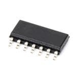
| 描述 | IC GATE NAND 4CH 2-INP 14-SOIC逻辑门 2-5.5V Quad 2-Input NAND |
| 产品分类 | |
| 品牌 | ON Semiconductor |
| 产品手册 | |
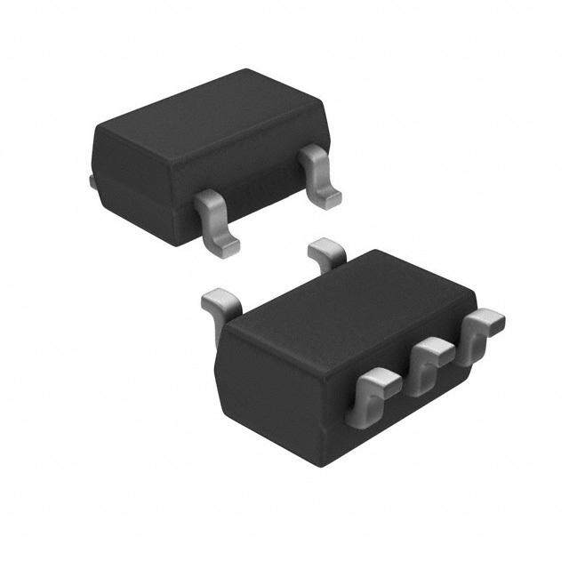
| 产品图片 |
|
| rohs | 符合RoHS无铅 / 符合限制有害物质指令(RoHS)规范要求 |
| 产品系列 | 逻辑集成电路,逻辑门,ON Semiconductor MC74VHC00DR2G74VHC |
| 数据手册 | |
| 产品型号 | MC74VHC00DR2G |
| 不同V、最大CL时的最大传播延迟 | 7.5ns @ 5V,50pF |
| 产品 | NAND |
| 产品种类 | 逻辑门 |
| 传播延迟时间 | 11.4 ns |
| 低电平输出电流 | 8 mA |
| 供应商器件封装 | 14-SOICN |
| 其它名称 | MC74VHC00DR2GOSCT |
| 包装 | 剪切带 (CT) |
| 商标 | ON Semiconductor |
| 安装类型 | 表面贴装 |
| 安装风格 | SMD/SMT |
| 封装 | Reel |
| 封装/外壳 | 14-SOIC(0.154",3.90mm 宽) |
| 封装/箱体 | SOIC-14 |
| 工作温度 | -55°C ~ 125°C |
| 工厂包装数量 | 2500 |
| 最大工作温度 | + 125 C |
| 最小工作温度 | - 55 C |
| 栅极数量 | 4 Gate |
| 标准包装 | 1 |
| 特性 | - |
| 电压-电源 | 2 V ~ 5.5 V |
| 电流-输出高,低 | 8mA,8mA |
| 电流-静态(最大值) | 2µA |
| 电源电压-最大 | 5.5 V |
| 电源电压-最小 | 2 V |
| 电路数 | 4 |
| 系列 | MC74VHC00 |
| 输入/输出线数量 | 2 / 1 |
| 输入数 | 2 |
| 输入线路数量 | 2 |
| 输出线路数量 | 1 |
| 逻辑电平-低 | 0.5V |
| 逻辑电平-高 | 1.5V |
| 逻辑类型 | 与非门 |
| 逻辑系列 | 74VHC |
| 高电平输出电流 | - 8 mA |


PDF Datasheet 数据手册内容提取
MC74VHC00 Quad 2-Input NAND Gate The MC74VHC00 is an advanced high speed CMOS 2−input NAND gate fabricated with silicon gate CMOS technology. It achieves high speed operation similar to equivalent Bipolar Schottky TTL while maintaining CMOS low power dissipation. The internal circuit is composed of three stages, including a buffer http://onsemi.com output which provides high noise immunity and stable output. The inputs tolerate voltages up to 7 V, allowing the interface of 5 V MARKING systems to 3 V systems. DIAGRAMS Features 14 • High Speed: tPD = 3.7 ns (Typ) at VCC = 5 V VHC00G • Low Power Dissipation: I = 2 (cid:2)A (Max) at T = 25°C SO−14 AWLYWW CC A • High Noise Immunity: V = V = 28% V D SUFFIX 1 NIH NIL CC CASE 751A • Power Down Protection Provided on Inputs • Balanced Propagation Delays • 14 Designed for 2 V to 5.5 V Operating Range • VHC Low Noise: V = 0.8 V (Max) OLP 00 • Pin and Function Compatible with Other Standard Logic Families TSSOP−14 ALYW(cid:2) DT SUFFIX (cid:2) • Latchup Performance Exceeds 300 mA CASE 948G 1 • ESD Performance: HBM > 2000 V; Machine Model > 200 V • Chip Complexity: 32 FETs or 8 Equivalent Gates • A = Assembly Location These Devices are Pb−Free and are RoHS Compliant L, WL = Wafer Lot Y = Year W, WW = Work Week G, (cid:2) = Pb−Free Device VCC B4 A4 Y4 B3 A3 Y3 14 13 12 11 10 9 8 ORDERING INFORMATION See detailed ordering and shipping information in the package dimensions section on page 4 of this data sheet. 1 2 3 4 5 6 7 A1 B1 Y1 A2 B2 Y2 GND Figure 1. Pinout: 14−Lead Packages (Top View) FUNCTION TABLE Inputs Output A B Y L L H L H H H L H H H L © Semiconductor Components Industries, LLC, 2014 1 Publication Order Number: September, 2014 − Rev. 7 MC74VHC00/D
MC74VHC00 1 A1 3 2 Y1 B1 4 A2 6 5 Y2 B2 Y = AB 9 A3 8 10 Y3 B3 12 A4 11 13 Y4 B4 Figure 2. Logic Diagram MAXIMUM RATINGS Symbol Parameter Value Unit VCC Positive DC Supply Voltage −0.5 to +7.0 V VIN Digital Input Voltage −0.5 to +7.0 V VOUT DC Output Voltage −0.5 to VCC +0.5 V IIK Input Diode Current −20 mA IOK Output Diode Current (cid:2)20 mA IOUT DC Output Current, per Pin (cid:2)25 mA ICC DC Supply Current, VCC and GND Pins (cid:2)75 mA PD Power Dissipation in Still Air SOIC Package 200 mW TSSOP 180 TSTG Storage Temperature Range −65 to +150 °C VESD ESD Withstand Voltage Human Body Model (Note 1) >2000 V Machine Model (Note 2) >200 Charged Device Model (Note 3) N/A ILATCH−UP Latch−Up Performance Above VCC and Below GND at 125°C (Note 4) (cid:2)300 mA (cid:3) Thermal Resistance, Junction to Ambient SOIC Package 143 °C/W JA TSSOP 164 Stresses exceeding those listed in the Maximum Ratings table may damage the device. If any of these limits are exceeded, device functionality should not be assumed, damage may occur and reliability may be affected. 1. Tested to EIA/JESD22−A114−A 2. Tested to EIA/JESD22−A115−A 3. Tested to JESD22−C101−A 4. Tested to EIA/JESD78 RECOMMENDED OPERATING CONDITIONS Symbol Characteristics Min Max Unit VCC DC Supply Voltage 2.0 5.5 V VIN DC Input Voltage 0 5.5 V VOUT DC Output Voltage 0 VCC V TA Operating Temperature Range, All Package Types −55 125 °C tr, tf Input Rise or Fall Time VCC = 3.3 V + 0.3 V 0 100 ns/V VCC = 5.0 V + 0.5 V 0 20 Functional operation above the stresses listed in the Recommended Operating Ranges is not implied. Extended exposure to stresses beyond the Recommended Operating Ranges limits may affect device reliability. http://onsemi.com 2
MC74VHC00 ÎÎÎÎÎÎÎÎÎÎÎÎÎÎÎÎÎÎÎÎÎÎÎÎÎÎÎÎÎÎÎÎÎ DC ELECTRICAL CHARACTERISTICS ÎÎÎÎÎÎÎÎÎÎÎÎÎÎÎÎÎÎÎÎÎÎÎÎÎÎÎÎÎÎÎÎÎÎÎÎÎÎÎÎÎÎÎÎÎÎÎÎÎÎÎÎÎÎÎÎÎÎÎÎÎÎÎÎÎÎÎÎÎÎÎÎÎ TA = −40 to TA = −55 to ÎÎÎÎÎÎÎÎÎÎÎÎÎÎÎÎÎÎÎÎÎÎÎÎÎÎÎÎÎÎÎÎÎÎÎÎÎÎVCCÎÎÎÎÎÎÎÎÎÎÎTÎÎÎÎA = ÎÎÎ25°CÎÎÎÎÎÎÎÎÎÎÎÎÎÎÎÎ85ÎÎÎΰC ÎÎÎÎÎÎÎÎÎÎÎÎ+12ÎÎÎÎ5°CÎÎÎÎÎÎÎÎÎ Symbol Parameter Test Conditions V Min Typ Max Min Max Min Max Unit ÎÎÎÎÎÎÎÎÎÎÎÎÎÎÎÎÎÎÎÎÎÎÎÎÎÎÎÎÎÎÎÎÎÎÎÎÎÎÎÎÎÎÎÎÎÎÎÎÎÎÎÎÎÎÎÎÎÎÎÎÎÎÎÎÎÎÎÎÎÎÎÎÎÎÎÎÎÎÎÎÎÎÎÎÎÎÎÎ VIH High−Level Input 2.0 1.50 1.50 1.50 V ÎÎÎÎÎVÎoltaÎge ÎÎÎÎÎÎÎÎÎÎÎÎ3.0 tÎÎo ÎVCÎC xÎÎÎÎÎÎÎÎVCÎC xÎÎÎÎÎVCÎC x ÎÎÎÎÎÎ 5.5 0.7 0.7 0.7 ÎÎÎÎÎÎÎÎÎÎÎÎÎÎÎÎÎÎÎÎÎÎÎÎÎÎÎÎÎÎÎÎÎÎÎÎÎÎÎÎÎÎÎÎÎÎÎÎÎÎÎÎÎÎÎÎÎÎÎÎÎÎÎÎÎÎÎÎÎÎÎÎÎÎÎÎÎÎÎÎÎÎÎÎÎÎÎÎ VIL Low−Level Input 2.0 0.50 0.50 0.50 V ÎÎÎÎÎÎÎÎÎÎÎÎÎÎÎÎÎÎÎÎÎÎÎÎÎÎÎÎÎÎÎÎÎÎÎÎÎÎÎÎÎÎÎÎ Voltage 3.0 to VCC x VCC x VCC x ÎÎÎÎÎÎÎÎÎÎÎÎÎÎÎÎÎÎÎÎÎÎÎÎÎÎÎÎÎÎÎÎÎÎÎÎÎÎ5.5ÎÎÎÎÎÎÎÎÎÎÎÎÎÎÎÎÎÎ0ÎÎ.3 ÎÎÎÎÎÎÎÎÎÎ0ÎÎ.3 ÎÎÎÎÎÎÎÎÎÎ0.ÎÎÎÎ3 ÎÎÎÎ ÎÎVÎOH ÎÎHÎigh−ÎLevÎel ÎÎÎVinÎ = VÎIH oÎr VILÎÎÎÎÎ2.0ÎÎÎ1Î.9 ÎÎ2Î.0 ÎÎÎÎÎ1Î.9 ÎÎÎÎÎ1Î.9 ÎÎÎÎÎVÎ Output Voltage IOH = − 50 (cid:2)A 3.0 2.9 3.0 2.9 2.9 ÎÎÎÎÎÎÎÎÎÎÎÎÎÎÎÎÎÎÎÎÎÎÎÎÎÎÎÎÎÎÎÎÎÎÎÎÎÎÎÎÎÎÎÎÎÎÎÎÎÎÎÎÎÎÎÎÎÎÎÎÎÎÎÎÎÎÎÎÎÎÎÎÎÎÎ 4.5 4.4 4.5 4.4 4.4 ÎÎÎÎÎÎÎÎÎÎÎÎÎÎÎÎÎÎÎÎÎÎÎÎÎÎÎÎÎÎÎÎÎÎÎÎÎÎÎÎÎÎÎÎ Vin = VIH or VIL ÎÎÎÎÎÎÎÎÎÎÎÎÎIOÎH = −Î 4 mÎA ÎÎÎ3.0ÎÎÎ2.Î58 ÎÎÎÎÎÎÎÎ2.Î48 ÎÎÎÎÎ2.Î40 ÎÎÎÎÎÎ IOH = − 8 mA 4.5 3.94 3.80 3.70 ÎÎÎÎÎÎÎÎÎÎÎÎÎÎÎÎÎÎÎÎÎÎÎÎÎÎÎÎÎÎÎÎÎÎÎÎÎÎÎÎÎÎÎÎÎÎÎÎÎÎÎÎÎÎÎÎÎÎÎÎÎÎÎÎÎÎÎÎÎÎÎÎÎÎÎÎÎÎÎÎÎÎÎÎÎÎÎÎ VOL Low−Level Vin = VIH or VIL 2.0 0.0 0.1 0.1 0.1 V ÎÎÎÎÎOÎutpuÎt VoÎltagÎe ÎÎIOÎL = 5Î0 (cid:2)AÎÎÎÎÎÎ3.0ÎÎÎÎÎÎ0Î.0 ÎÎ0Î.1 ÎÎÎÎÎ0Î.1 ÎÎÎÎÎ0.ÎÎ1 ÎÎ ÎÎÎÎÎÎÎÎÎÎÎÎÎÎÎÎÎÎÎÎÎÎÎÎÎÎÎÎ4.5ÎÎÎÎÎÎÎÎÎÎÎÎ0ÎÎ.0 ÎÎÎÎ0ÎÎ.1 ÎÎÎÎÎÎÎÎÎÎ0ÎÎ.1 ÎÎÎÎÎÎÎÎÎÎ0.ÎÎÎ1 ÎÎ ÎÎÎÎÎÎÎÎÎÎÎVinÎ = VÎIH oÎr VILÎÎÎÎÎÎÎÎÎÎÎÎÎÎÎÎÎÎÎÎÎÎÎÎÎÎÎÎÎÎ IOL = 4 mA 3.0 0.36 0.44 0.55 ÎÎÎÎÎÎÎÎÎÎÎÎÎÎÎÎÎÎÎÎÎÎÎÎÎÎIOÎÎL = 8ÎÎ mAÎÎÎÎÎÎÎÎ4.5ÎÎÎÎÎÎÎÎÎÎÎÎÎÎÎÎÎÎ0ÎÎ.36 ÎÎÎÎÎÎÎÎÎÎ0.ÎÎ44 ÎÎÎÎÎÎÎÎÎÎ0.5ÎÎÎÎ5 ÎÎÎÎ ÎÎIÎin ÎÎIÎnputÎ LeaÎkageÎÎÎVinÎ = 5Î.5 VÎ or GÎNDÎÎÎ0Î to 5ÎÎ.5 ÎÎÎÎÎÎÎ(cid:2)Î0.1ÎÎÎÎÎ(cid:2)Î1.0 ÎÎÎÎÎ(cid:2)2ÎÎ.0 Î(cid:2)AÎ ÎÎÎÎÎÎÎÎÎÎCÎÎurreÎÎnt ÎÎÎÎÎÎÎÎÎÎÎÎÎÎÎÎÎÎÎÎÎÎÎÎÎÎÎÎÎÎÎÎÎÎÎÎÎÎÎÎÎÎÎÎÎÎÎÎÎÎÎÎÎÎÎÎÎÎÎÎÎÎÎÎÎÎÎÎÎÎÎÎÎÎ ÎÎICÎC ÎÎQÎuiesÎcenÎt SupÎplyÎÎVinÎ = VÎCC oÎr GNÎD ÎÎÎÎ5.5ÎÎÎÎÎÎÎÎÎ2Î.0 ÎÎÎÎÎ2Î0 ÎÎÎÎÎ4ÎÎ0 Î(cid:2)AÎ Current ÎÎÎÎÎÎÎÎÎÎÎÎÎÎÎÎÎÎÎÎÎÎÎÎÎÎÎÎÎÎÎÎÎÎÎÎÎÎÎÎÎÎÎÎ Product parametric performance is indicated in the Electrical Characteristics for the listed test conditions, unless otherwise noted. Product performance may not be indicated by the Electrical Characteristics if operated under different conditions. ÎÎÎÎÎÎÎÎÎÎÎÎÎÎÎÎÎÎÎÎÎÎÎÎÎÎÎÎÎÎÎÎÎ AC ELECTRICAL CHARACTERISTICS (Input tr = tf = 3.0 ns) ÎÎÎÎÎÎÎÎÎÎÎÎÎÎÎÎÎÎÎÎÎÎÎÎÎÎÎÎÎÎÎÎÎÎÎÎÎÎÎÎÎÎÎÎÎÎÎÎÎÎÎÎÎÎÎÎÎÎÎÎÎÎÎÎÎÎÎÎÎÎÎÎ TA = −40 to TA = −55 to ÎÎÎÎÎÎÎÎÎÎÎÎÎÎÎÎÎÎÎÎÎÎÎÎÎÎÎTA =ÎÎ 25°ÎÎÎC ÎÎÎÎÎÎÎÎ85ÎÎΰC ÎÎÎÎÎÎÎÎ+12ÎÎÎ5°CÎÎÎÎÎ ÎÎÎÎSymÎÎboÎÎÎÎl ÎÎPÎÎaramÎÎeterÎÎÎÎÎÎÎÎÎÎTÎÎest ÎÎConÎÎditioÎÎns ÎÎÎÎÎÎÎÎMÎÎin ÎÎÎÎTÎÎyp ÎÎÎÎMÎÎax ÎÎÎÎMÎÎin ÎÎÎÎMÎÎax ÎÎÎÎMÎÎin ÎÎÎÎMaÎÎÎÎx ÎÎUnÎÎit ÎÎtPÎLH, ÎÎPÎropaÎgatiÎon ÎÎÎVCÎC = Î3.3 ±Î 0.3Î V ÎCÎL = Î15 pÎF ÎÎÎÎÎ5Î.5 ÎÎ7Î.9 ÎÎ1Î.0 ÎÎ9Î.5 ÎÎ1Î.0 ÎÎ1ÎÎ0 ÎnsÎ ÎÎÎÎtPÎÎHL ÎÎÎDÎelayÎ, A oÎr B Îto YÎÎÎÎÎÎÎÎÎÎÎÎÎCÎÎL = ÎÎ50 pÎÎF ÎÎÎÎÎÎÎÎÎÎ8ÎÎ.0 ÎÎÎÎ1ÎÎ1.4 ÎÎÎÎ1ÎÎ.0 ÎÎÎÎ13ÎÎ.0 ÎÎÎÎ1ÎÎ.0 ÎÎÎÎ14ÎÎÎÎ.5 ÎÎÎÎ ÎÎÎÎÎÎÎÎÎÎÎVCÎC = Î5.0 ±Î 0.5Î V ÎCÎL = Î15 pÎF ÎÎÎÎÎ3Î.7 ÎÎ5Î.5 ÎÎ1Î.0 ÎÎ6Î.5 ÎÎ1Î.0 ÎÎ7.ÎÎ0 ÎÎ CL = 50 pF 5.2 7.5 1.0 8.5 1.0 9.5 ÎÎÎÎÎÎÎÎÎÎÎÎÎÎÎÎÎÎÎÎÎÎÎÎÎÎÎÎÎÎÎÎÎÎÎÎÎÎÎÎÎÎÎÎÎÎÎÎÎÎÎÎÎÎÎÎÎÎÎÎÎÎÎÎÎÎÎÎÎÎÎÎÎÎÎÎÎÎÎÎÎÎÎÎÎÎ Cin Input 4.0 10 10 10 pF ÎÎÎÎÎÎÎÎÎÎÎÎÎÎÎÎÎÎÎÎÎÎÎÎÎÎÎÎÎÎÎÎÎÎÎÎÎÎÎÎÎÎÎ Capacitance ÎÎÎÎÎÎÎÎÎÎÎÎÎÎÎÎÎÎÎÎÎÎÎÎÎÎÎÎÎÎÎÎÎÎÎÎÎÎÎÎÎÎÎ Typical @ 25°C, VCC = 5.0 V CPD Power Dissipation Capacitance (Note 5) 19 pF 5. CPD is defined as the value of the internal equivalent capacitance which is calculated from the operating current consumption without load. Average operating current can be obtained by the equation: ICC(OPR) = CPD (cid:2) VCC (cid:2) fin + ICC/4 (per gate). CPD is used to determine the no−load dynamic power consumption; PD = CPD (cid:2) VCC2 (cid:2) fin + ICC (cid:2) VCC. NOISE CHARACTERISTICS (Input tr = tf = 3.0 ns, CL = 50 pF, VCC = 5.0 V, Measured in SOIC Package) TA = 25°C Symbol Characteristic Typ Max Unit VOLP Quiet Output Maximum Dynamic VOL 0.3 0.8 V VOLV Quiet Output Minimum Dynamic VOL − 0.3 − 0.8 V VIHD Minimum High Level Dynamic Input Voltage 3.5 V VILD Maximum Low Level Dynamic Input Voltage 1.5 V http://onsemi.com 3
MC74VHC00 TEST POINT A or B VCC OUTPUT 50% GND DEVICE UNDER tPLH tPHL TEST CL* Y 50% VCC *Includes all probe and jig capacitance Figure 3. Switching Waveforms Figure 4. Test Circuit INPUT Figure 5. Input Equivalent Circuit ORDERING INFORMATION Device Package Shipping† MC74VHC00DR2G SOIC−14 2500 / Tape & Reel (Pb−Free) MC74VHC00DTG TSSOP−14* 96 Units / Rail (Pb−Free) MC74VHC00DTR2G TSSOP−14* 2500 / Tape & Reel (Pb−Free) †For information on tape and reel specifications, including part orientation and tape sizes, please refer to our Tape and Reel Packaging Specifications Brochure, BRD8011/D. *This package is inherently Pb−Free. http://onsemi.com 4
MC74VHC00 PACKAGE DIMENSIONS SOIC−14 CASE 751A−03 ISSUE K D A NOTES: B 1.DIMENSIONING AND TOLERANCING PER ASME Y14.5M, 1994. 2.CONTROLLING DIMENSION: MILLIMETERS. 14 8 3.DIMENSION b DOES NOT INCLUDE DAMBAR A3 PROTRUSION. ALLOWABLE PROTRUSION SHALL BE 0.13 TOTAL IN EXCESS OF AT MAXIMUM MATERIAL CONDITION. H E 4.DIMENSIONS D AND E DO NOT INCLUDE MOLD PROTRUSIONS. L 5.MAXIMUM MOLD PROTRUSION 0.15 PER SIDE. 1 7 DETAIL A MILLIMETERS INCHES 0.25 M B M 13Xb DIM MIN MAX MIN MAX A 1.35 1.75 0.054 0.068 0.25 M C A S B S A1 0.10 0.25 0.004 0.010 A3 0.19 0.25 0.008 0.010 DETAIL A b 0.35 0.49 0.014 0.019 h A D 8.55 8.75 0.337 0.344 X 45(cid:3) E 3.80 4.00 0.150 0.157 e 1.27 BSC 0.050 BSC H 5.80 6.20 0.228 0.244 h 0.25 0.50 0.010 0.019 e A1 C SEATING M ML 0.04 0(cid:3) 1.72 5(cid:3) 0.001 6(cid:3) 0.074 9(cid:3) PLANE SOLDERING FOOTPRINT* 6.50 14X 1.18 1 1.27 PITCH 14X 0.58 DIMENSIONS: MILLIMETERS *For additional information on our Pb−Free strategy and soldering details, please download the ON Semiconductor Soldering and Mounting Techniques Reference Manual, SOLDERRM/D. http://onsemi.com 5
MC74VHC00 PACKAGE DIMENSIONS TSSOP−14 CASE 948G ISSUE B 14X K REF NOTES: 1. DIMENSIONING AND TOLERANCING PER 0.10 (0.004) M T U S V S ANSI Y14.5M, 1982. 2. CONTROLLING DIMENSION: MILLIMETER. 0.15 (0.006) T U S 3. DIMENSION A DOES NOT INCLUDE MOLD FLASH, PROTRUSIONS OR GATE BURRS. N MOLD FLASH OR GATE BURRS SHALL NOT 0.25 (0.010) EXCEED 0.15 (0.006) PER SIDE. 2XL/2 14 8 4I.NTDEIMRLEENASDIO FNL ABS DHO OERS PNROOT TINRCULSUIODNE. M INTERLEAD FLASH OR PROTRUSION SHALL NOT EXCEED 0.25 (0.010) PER SIDE. L B 5. DIMENSION K DOES NOT INCLUDE −U− N DAMBAR PROTRUSION. ALLOWABLE PIN 1 DAMBAR PROTRUSION SHALL BE 0.08 IDENT. F (0.003) TOTAL IN EXCESS OF THE K DIMENSION AT MAXIMUM MATERIAL 1 7 DETAIL E CONDITION. 6. TERMINAL NUMBERS ARE SHOWN FOR REFERENCE ONLY. 7. DIMENSION A AND B ARE TO BE 0.15 (0.006) T U S A K DETERMINED AT DATUM PLANE −W−. −V− ÇÉÇÉK1ÇÉ MILLIMETERS INCHES DIM MIN MAX MIN MAX J J1 ÇÉÇÉÇÉ A 4.90 5.10 0.193 0.200 B 4.30 4.50 0.169 0.177 C −−− 1.20 −−− 0.047 SECTION N−N D 0.05 0.15 0.002 0.006 F 0.50 0.75 0.020 0.030 G 0.65 BSC 0.026 BSC H 0.50 0.60 0.020 0.024 −W− J 0.09 0.20 0.004 0.008 C J1 0.09 0.16 0.004 0.006 K 0.19 0.30 0.007 0.012 0.10 (0.004) K1 0.19 0.25 0.007 0.010 −T− SPELAATNIENG D G H DETAIL E ML 06 .(cid:3) 4 0 BS8C (cid:3) 00. 2(cid:3) 52 BS8C (cid:3) SOLDERING FOOTPRINT 7.06 1 0.65 PITCH 14X 14X 0.36 1.26 DIMENSIONS: MILLIMETERS ON Semiconductor and the are registered trademarks of Semiconductor Components Industries, LLC (SCILLC) or its subsidiaries in the United States and/or other countries. SCILLC owns the rights to a number of patents, trademarks, copyrights, trade secrets, and other intellectual property. A listing of SCILLC’s product/patent coverage may be accessed at www.onsemi.com/site/pdf/Patent−Marking.pdf. SCILLC reserves the right to make changes without further notice to any products herein. SCILLC makes no warranty, representation or guarantee regarding the suitability of its products for any particular purpose, nor does SCILLC assume any liability arising out of the application or use of any product or circuit, and specifically disclaims any and all liability, including without limitation special, consequential or incidental damages. “Typical” parameters which may be provided in SCILLC data sheets and/or specifications can and do vary in different applications and actual performance may vary over time. All operating parameters, including “Typicals” must be validated for each customer application by customer’s technical experts. SCILLC does not convey any license under its patent rights nor the rights of others. SCILLC products are not designed, intended, or authorized for use as components in systems intended for surgical implant into the body, or other applications intended to support or sustain life, or for any other application in which the failure of the SCILLC product could create a situation where personal injury or death may occur. Should Buyer purchase or use SCILLC products for any such unintended or unauthorized application, Buyer shall indemnify and hold SCILLC and its officers, employees, subsidiaries, affiliates, and distributors harmless against all claims, costs, damages, and expenses, and reasonable attorney fees arising out of, directly or indirectly, any claim of personal injury or death associated with such unintended or unauthorized use, even if such claim alleges that SCILLC was negligent regarding the design or manufacture of the part. SCILLC is an Equal Opportunity/Affirmative Action Employer. This literature is subject to all applicable copyright laws and is not for resale in any manner. PUBLICATION ORDERING INFORMATION LITERATURE FULFILLMENT: N. American Technical Support: 800−282−9855 Toll Free ON Semiconductor Website: www.onsemi.com Literature Distribution Center for ON Semiconductor USA/Canada P.O. Box 5163, Denver, Colorado 80217 USA Europe, Middle East and Africa Technical Support: Order Literature: http://www.onsemi.com/orderlit Phone: 303−675−2175 or 800−344−3860 Toll Free USA/Canada Phone: 421 33 790 2910 Fax: 303−675−2176 or 800−344−3867 Toll Free USA/Canada Japan Customer Focus Center For additional information, please contact your local Email: orderlit@onsemi.com Phone: 81−3−5817−1050 Sales Representative http://onsemi.com MC74VHC00/D 6