ICGOO在线商城 > 集成电路(IC) > 逻辑 - 缓冲器,驱动器,接收器,收发器 > MC74LVX4245DTR2G
 Datasheet下载
- 型号: MC74LVX4245DTR2G
- 制造商: ON Semiconductor
- 库位|库存: xxxx|xxxx
- 要求:
| 数量阶梯 | 香港交货 | 国内含税 |
| +xxxx | $xxxx | ¥xxxx |
查看当月历史价格
查看今年历史价格
MC74LVX4245DTR2G产品简介:
ICGOO电子元器件商城为您提供MC74LVX4245DTR2G由ON Semiconductor设计生产,在icgoo商城现货销售,并且可以通过原厂、代理商等渠道进行代购。 MC74LVX4245DTR2G价格参考¥5.85-¥11.74。ON SemiconductorMC74LVX4245DTR2G封装/规格:逻辑 - 缓冲器,驱动器,接收器,收发器, Transceiver, Non-Inverting 1 Element 8 Bit per Element 3-State Output 24-TSSOP。您可以下载MC74LVX4245DTR2G参考资料、Datasheet数据手册功能说明书,资料中有MC74LVX4245DTR2G 详细功能的应用电路图电压和使用方法及教程。
| 参数 | 数值 |
| 产品目录 | 集成电路 (IC)半导体 |
| 描述 | IC TXRX DUAL OCT 3ST LV 24TSSOP总线收发器 Dual Supply Octal Translating |
| 产品分类 | |
| 品牌 | ON Semiconductor |
| 产品手册 | |
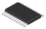
| 产品图片 |
|
| rohs | 符合RoHS无铅 / 符合限制有害物质指令(RoHS)规范要求 |
| 产品系列 | 逻辑集成电路,总线收发器,ON Semiconductor MC74LVX4245DTR2G74LVX |
| 数据手册 | |
| 产品型号 | MC74LVX4245DTR2G |
| 产品种类 | 总线收发器 |
| 传播延迟时间 | 10 ns |
| 低电平输出电流 | 24 mA |
| 供应商器件封装 | 24-TSSOP |
| 元件数 | 1 |
| 其它名称 | MC74LVX4245DTR2GOSDKR |
| 功能 | Bus Transceiver with Voltage Translation |
| 包装 | Digi-Reel® |
| 商标 | ON Semiconductor |
| 安装类型 | 表面贴装 |
| 安装风格 | SMD/SMT |
| 封装 | Reel |
| 封装/外壳 | 24-TSSOP(0.173",4.40mm 宽) |
| 封装/箱体 | TSSOP-24 |
| 工作温度 | -40°C ~ 85°C |
| 工厂包装数量 | 2500 |
| 最大功率耗散 | 200 mW |
| 最大工作温度 | + 85 C |
| 最小工作温度 | - 40 C |
| 极性 | Non-Inverting |
| 标准包装 | 1 |
| 每元件位数 | 8 |
| 每芯片的通道数量 | 8 |
| 电压-电源 | 2.7 V ~ 3.6 V,4.5 V ~ 5.5 V |
| 电流-输出高,低 | 12mA,12mA; 24mA,24mA |
| 电源电压-最大 | 3.6 V, 5.5 V |
| 电源电压-最小 | 2.7 V, 4.5 V |
| 电路数量 | 2 |
| 系列 | MC74LVX4245 |
| 输入电平 | CMOS |
| 输出电平 | CMOS |
| 输出类型 | 3-State |
| 逻辑类型 | CMOS |
| 逻辑系列 | 74LVX |
| 高电平输出电流 | - 24 mA |


- 商务部:美国ITC正式对集成电路等产品启动337调查
- 曝三星4nm工艺存在良率问题 高通将骁龙8 Gen1或转产台积电
- 太阳诱电将投资9.5亿元在常州建新厂生产MLCC 预计2023年完工
- 英特尔发布欧洲新工厂建设计划 深化IDM 2.0 战略
- 台积电先进制程称霸业界 有大客户加持明年业绩稳了
- 达到5530亿美元!SIA预计今年全球半导体销售额将创下新高
- 英特尔拟将自动驾驶子公司Mobileye上市 估值或超500亿美元
- 三星加码芯片和SET,合并消费电子和移动部门,撤换高东真等 CEO
- 三星电子宣布重大人事变动 还合并消费电子和移动部门
- 海关总署:前11个月进口集成电路产品价值2.52万亿元 增长14.8%


PDF Datasheet 数据手册内容提取
MC74LVX4245 Dual Supply Octal Translating Transceiver with 3−State Outputs The 74LVX4245 is a 24−pin dual−supply, octal translating www.onsemi.com transceiver that is designed to interface between a 5.0 V bus and a 3.0 V bus in a mixed 3.0 V / 5.0 V supply environment such as laptop MARKING computers using a 3.3 V CPU and 5.0 V LCD display. The A port DIAGRAMS interfaces with the 5V bus; the B port interfaces with the 3.0 V bus. The Transmit/Receive (T/R) input determines the direction of data 24 flow. Transmit (active−High) enables data from the A port to the B 24 port. Receive (active−Low) enables data from the B port to the A port. SOIC−24 LVX4245 The Output Enable (OE) input, when High, disables both A and B DW SUFFIX AWLYYWWG CASE 751E ports by placing them in 3−State. 1 1 Features • Bi−directional Interface Between 5.0 V and 3.0 V Buses 24 • Control Inputs Compatible with TTL Level • 5.0 V Data Flow at A Port and 3.0 V Data Flow at B Port 24 TSSOP−24 LVX 4245G • DT SUFFIX Outputs Source/Sink 24 mA at 5.0 V Bus and 12 mA at 3.0 V Bus ALYW CASE 948H • 1 Guaranteed Simultaneous Switching Noise Level and Dynamic Threshold Performance 1 • Available in SOIC and TSSOP Packages LVX4245 = Specific Device Code • Functionally Compatible with the 74 Series 245 A = Assembly Location • WL, L = Wafer Lot NLV Prefix for Automotive and Other Applications Requiring Y = Year Unique Site and Control Change Requirements; AEC−Q100 WW, W = Work Week Qualified and PPAP Capable G or (cid:2) = Pb−Free Package • These Devices are Pb−Free, Halogen Free/BFR Free and are RoHS (Note: Microdot may be in either location) Compliant PIN NAMES Pins Function VCCB VCCB OE B0 B1 B2 B3 B4 B5 B6 B7 GND OE Output Enable Input 24 23 22 21 20 19 18 17 16 15 14 13 T/R Transmit/Receive Input A0−A7 Side A 3−State Inputs or 3−State Outputs B0−B7 Side B 3−State Inputs or 3−State Outputs 1 2 3 4 5 6 7 8 9 10 11 12 ORDERING INFORMATION VCCA T/R A0 A1 A2 A3 A4 A5 A6 A7 GND GND See detailed ordering and shipping information in the package dimensions section on page 5 of this data sheet. Figure 1. 24−Lead Pinout (Top View) © Semiconductor Components Industries, LLC, 2011 1 Publication Order Number: July, 2017 − Rev. 6 MC74LVX4245/D
MC74LVX4245 OE 22 T/R 2 3 A0 21 B0 4 A1 20 B1 5 A2 19 B2 6 A3 18 B3 7 A4 17 B4 8 A5 16 B5 9 A6 15 B6 10 A7 14 B7 Figure 2. Logic Diagram INPUTS OPERATING MODE OE T/R Non−Inverting L L B Data to A Bus L H A Data to B Bus H X Z H = High Voltage Level; L = Low Voltage Level; Z = High Impedance State; X = High or Low Voltage Level and Transitions are Acceptable; For ICC reasons, Do Not Float Inputs www.onsemi.com 2
MC74LVX4245 ABSOLUTE MAXIMUM RATINGS Symbol Parameter Value Condition Unit VCCA, DC Supply Voltage −0.5 to +7.0 V VCCB VI DC Input Voltage OE, T/R −0.5 to VCCA +0.5 V VI/O DC Input/Output Voltage An −0.5 to VCCA +0.5 V Bn −0.5 to VCCB +0.5 V IIK DC Input Diode Current OE, T/R ±20 VI < GND mA IOK DC Output Diode Current ±50 VO < GND; VO > VCC mA IO DC Output Source/Sink Current ±50 mA ICC, DC Supply Current Per Output Pin ±50 mA IGND Maximum Current at ICCA ±200 Maximum Current at ICCB ±100 TSTG Storage Temperature Range −65 to +150 °C Latchup DC Latchup Source/Sink Current ±300 mA Stresses exceeding those listed in the Maximum Ratings table may damage the device. If any of these limits are exceeded, device functionality should not be assumed, damage may occur and reliability may be affected. RECOMMENDED OPERATING CONDITIONS Symbol Parameter Min Max Unit VCCA, Supply Voltage VCCA 4.5 5.5 V VCCB VCCB 2.7 3.6 VI Input Voltage OE, T/R 0 VCCA V VI/O Input/Output Voltage An 0 VCCA V Bn 0 VCCB TA Operating Free−Air Temperature −40 +85 °C (cid:2)t/(cid:2)V Minimum Input Edge Rate 0 8 ns/V VIN from 30% to 70% of VCC; VCC at 3.0V, 4.5V, 5.5V Functional operation above the stresses listed in the Recommended Operating Ranges is not implied. Extended exposure to stresses beyond the Recommended Operating Ranges limits may affect device reliability. DC ELECTRICAL CHARACTERISTICS TA = 25°C TA = −40 to +85°C Symbol Parameter Condition VCCA VCCB Typ Guaranteed Limits Unit VIHA Minimum HIGH An,OE 5.5 3.3 2.0 2.0 V Level T/R VOUT ≤ 0.1V 4.5 3.3 2.0 2.0 Input Voltage or VIHB Bn ≥ VCC − 0.1V 5.0 3.6 2.0 2.0 V 5.0 2.7 2.0 2.0 VILA Maximum LOW An,OE 5.5 3.3 0.8 0.8 V Level T/R VOUT ≤ 0.1V 4.5 3.3 0.8 0.8 Input Voltage or VILB Bn ≥ VCC − 0.1V 5.0 2.7 0.8 0.8 V 5.0 3.6 0.8 0.8 VOHA Minimum HIGH IOUT = −100(cid:3)A 4.5 3.0 4.50 4.40 4.40 V Level IOH = −24mA 4.5 3.0 4.25 3.86 3.76 Output Voltage VOHB IOUT = −100(cid:3)A 4.5 3.0 2.99 2.9 2.9 V IOH = −12mA 4.5 3.0 2.80 2.4 2.4 IOH = −8mA 4.5 2.7 2.50 2.4 2.4 VOLA Maximum LOW IOUT = 100(cid:3)A 4.5 3.0 0.002 0.10 0.10 V Level IOL = 24mA 4.5 3.0 0.18 0.36 0.44 Output Voltage VOLB IOUT = 100(cid:3)A 4.5 3.0 0.002 0.10 0.10 V IOL = 12mA 4.5 3.0 0.1 0.31 0.40 IOL = 8mA 4.5 2.7 0.1 0.31 0.40 www.onsemi.com 3
MC74LVX4245 DC ELECTRICAL CHARACTERISTICS TA = 25°C TA = −40 to +85°C Symbol Parameter Condition VCCA VCCB Typ Guaranteed Limits Unit IIN Max Input Leak- OE, (cid:3)A age T/R VI = VCCA, GND 5.5 3.6 ±0.1 ±1.0 Current IOZA Max 3−State Out- VI = VIH, VIL (cid:3)A put Leakage An OE = VCCA 5.5 3.6 ±0.5 ±5.0 VO = VCCA, GND IOZB Max 3−State Out- VI = VIH, VIL (cid:3)A put Leakage Bn OE = VCCA 5.5 3.6 ±0.5 ±5.0 VO = VCCB, GND (cid:2)ICC Mpearx Iinmpuumt ICCT An,TO/RE VI=VCCA−2.1V 5.5 3.6 1.0 1.35 1.5 mA Bn VI=VCCB−0.6V 5.5 3.6 0.35 0.5 mA ICCA Quiescent VCCA An=VCCA or GND (cid:3)A Supply Current Bn=VCCB or GND 5.5 3.6 8 80 OE=GND T/R=GND ICCB Quiescent VCCB An=VCCA or GND (cid:3)A Supply Current Bn=VCCB or GND 5.5 3.6 5 50 OE=GND T/R=VCCA VOLPA Quiet Output Max Notes 1, 2 5.0 3.3 1.5 V VOLPB Dynamic VOL 5.0 3.3 1.2 VOLVA Quiet Output Min Notes 1, 2 5.0 3.3 −1.2 V VOLVB Dynamic VOL 5.0 3.3 −0.8 VIHDA Min HIGH Level 5.0 3.3 2.0 V VIHDB Dynamic Input Notes 1, 3 5.0 3.3 2.0 Voltage VILDA Max LOW Level 5.0 3.3 0.8 V VILDB Dynamic Input Notes 1, 3 5.0 3.3 0.8 Voltage Product parametric performance is indicated in the Electrical Characteristics for the listed test conditions, unless otherwise noted. Product performance may not be indicated by the Electrical Characteristics if operated under different conditions. 1. Worst case package. 2. Max number of outputs defined as (n). Data inputs are driven 0V to VCC level; one output at GND. 3. Max number of data inputs (n) switching. (n−1) inputs switching 0V to VCC level. Input under test switching: VCC level to threshold (VIHD), 0V to threshold (VILD), f = 1MHz. CAPACITIVE CHARACTERISTICS Symbol Parameter Condition Typical Unit CIN Input Capacitance VCCA = 5.0V; VCCB = 3.3V 4.5 pF CI/O Input/Output Capacitance VCCA = 5.0V; VCCB = 3.3V 15 pF CPD Power Dissipation Capacitance B→A VCCA = 5.0V 55 pF (Measured at 10MHz) A→B VCCB = 3.3V 40 www.onsemi.com 4
MC74LVX4245 AC ELECTRICAL CHARACTERISTICS TA = −40 to +85°C TA = −40 to +85°C CL = 50pF CL = 50pF VCCA = 5V ±0.5V VCCA = 5V ±0.5V VCCB = 3.3V ±0.3V VCCB = 2.7V Typ Symbol Parameter Min (Note 4) Max Min Max Unit tPHL Propagation Delay A to B 1.0 5.1 9.0 1.0 10.0 ns tPLH 1.0 5.3 9.0 1.0 10.0 tPHL Propagation Delay B to A 1.0 5.4 9.0 1.0 10.0 ns tPLH 1.0 5.5 9.0 1.0 10.0 tPZL Output Enable Time OE to B 1.0 6.5 10.5 1.0 11.5 ns tPZH 1.0 6.7 10.5 1.0 11.5 tPZL Output Enable Time OE to A 1.0 5.2 9.5 1.0 10.0 ns tPZH 1.0 5.8 9.5 1.0 10.0 tPHZ Output Disable Time OE to B 1.0 6.0 10.0 1.0 10.0 ns tPLZ 1.0 3.3 7.0 1.0 7.5 tPHZ Output Disable Time OE to A 1.0 3.9 7.5 1.0 7.5 ns tPLZ 1.0 2.9 7.0 1.0 7.5 tOSHL Output to Output Skew, Data to Output (Note 5) 1.0 1.5 1.5 ns tOSLH 4. Typical values at VCCA = 5.0V; VCCB = 3.3V at 25°C. 5. Skew is defined as the absolute value of the difference between the actual propagation delay for any two separate outputs of the same device. The specification applies to any outputs switching in the same direction, either HIGH−to−LOW (tOSHL) or LOW−to−HIGH (tOSLH); parameter guaranteed by design. ORDERING INFORMATION Device Package Shipping† MC74LVX4245DWG 30 Units / Rail SOIC−24 MC74LVX4245DWR2G (Pb−Free) 1000 / Tape & Reel MC74LVX4245DTG 62 Units / Rail TSSOP−24 MC74LVX4245DTR2G 2500 / Tape & Reel (Pb−Free) NLVLVX4245DTR2G* 2500 / Tape & Reel †For information on tape and reel specifications, including part orientation and tape sizes, please refer to our Tape and Reel Packaging Specifications Brochure, BRD8011/D. *NLV Prefix for Automotive and Other Applications Requiring Unique Site and Control Change Requirements; AEC−Q100 Qualified and PPAP Capable. www.onsemi.com 5
MC74LVX4245 Dual Supply Octal Translating Transceiver The 74LVX4245 is a is a dual−supply device well capable of bidirectional signal voltage translation. This level shifting LOW VOLTAGE CPU LOCAL BUS ability provides an excellent interface between low voltage CPU local bus and a standard 5.0 V I/O bus. The device control inputs can be controlled by either the low voltage VCCB VCCB CPU and core logic or a bus arbitrator with 5.0 V I/O levels. LVX4245 LVX4245 The LVX4245 is ideal for mixed voltage applications such as notebook computers using a 3.3 V CPU and 5.0 V VCCA VCCA peripheral devices. Applications: EISA - ISA - MCA Mixed Mode Dual Supply Interface Solutions (5V I/O LEVELS) The LVX4245 is designed to solve 3.0 V / 5.0 V interfaces when CMOS devices cannot tolerate I/O levels above their Figure 3. 3.3V/5V Interface Block Diagram applied V . If an I/O pin of a 3.0 V device is driven by a 5.0 CC V device, the P−Channel transistor in the 3.0 V device will Powering Up the LVX4245 conduct − causing current flow from the I/O bus to the 3.0 V When powering up the LVX4245, please note that if the power supply. The result may be destruction of the 3.0 V V pin is powered−up well in advance of the V pin, CCB CCA device through latchup effects. A current limiting resistor several milliamps of either I or I current will result. CCA CCB may be used to prevent destruction, but it causes speed If the V pin is powered−up in advance of the V pin CCA CCB degradation and needless power dissipation. then only nanoamps of Icc current will result. In actuality the A better solution is provided in the LVX4245. It provides V can be powered “slightly” before the V without CCB CCA two different output levels that easily handle the dual voltage the current penalty, but this “setup time” is dependent on the interface. The A port is a dedicated 5.0 V port; the B port is power−up ramp rate of the V pins. With a ramp rate of CC a dedicated 3.0 V port. approximately 50 mV/ns (50V/(cid:3)s) a 25 ns setup time was Since the LVX4245 is a ‘245 transceiver, the user may observed (V before V ). With a 7.0 V/(cid:3)s rate, the CCB CCA either use it for bidirectional or unidirectional applications. setup time was about 140ns. When all is said and done, the The center 20 pins are configured to match a ‘245 pinout. safest powerup strategy is to simply power V before CCA This enables the user to easily replace this level shifter with V . One more note: if the V ramp rate is faster than CCB CCB a 3.0 V ‘245 device without additional layout work or re− the V ramp rate then power problems might still occur, CCA manufacture of the circuit board (when both buses are 3.0 V). even if the V powerup began prior to the V powerup. CCA CCB www.onsemi.com 6
MC74LVX4245 MICROCHANNEL/ EISA/ISA/AT LOCAL 5V 5V BUS 3V BUS 3V KEYBOARD CONTROLLER CACHE SRAM SUPER 5V 3V I/O VCCA VCCB CPU CORE 386/486 LOGIC LVX4245 A PORT B PORT TRANSCEIVERS A0:7 B0:7 ROM BIOS PCMCIA CONTROLLER MEMORY VGA DRIVER CONTROLLER Figure 4. MC74LVX4245 Fits Into a System with 3V Subsystem and 5V Subsystem VCCA MC74LVX4245 VCCB (T/R) DIR VCCB A0 OE A1 B0 A2 B1 STANDARD A3 B2 74 SERIES A4 `245 B3 A5 B4 A6 B5 A7 B6 GND B7 GND GND Figure 5. MC74LVX4245 Pin Arrangement Is Compatible to 20−Pin 74 Series ‘245s www.onsemi.com 7
MC74LVX4245 VCC An, Bn 50% VCC 50% VCC 0V tPLH tPHL VOH Bn, An 50% VCC 50% VCC VOL WAVEFORM 1 - PROPAGATION DELAYS tR = tF = 2.5ns, 10% to 90%; f = 1MHz; tW = 500ns VCCA OE, T/R 50% VCC 50% VCC 0V tPZH tPHZ VCC VOH - 0.3V An, Bn 50% VCC ≈ 0V tPZL tPLZ ≈ VCC An, Bn 50% VCC VOL + 0.3V GND WAVEFORM 2 - OUTPUT ENABLE AND DISABLE TIMES tR = tF = 2.5ns, 10% to 90%; f = 1MHz; tW = 500ns Figure 6. AC Waveforms VCC 2 × VCC OPEN PULSE R1 DUT GENERATOR RT CL RL TEST SWITCH tPLH, tPHL, tPZH, tPHZ Open tPZL, tPLZ 2 × VCC CL = 50pF or equivalent (Includes jig and probe capacitance) RL = R1 = 500(cid:4) or equivalent RT = ZOUT of pulse generator (typically 50(cid:4)) Figure 7. Test Circuit www.onsemi.com 8
MC74LVX4245 PACKAGE DIMENSIONS SOIC−24 DW SUFFIX CASE 751E−04 ISSUE F NOTES: 1. DIMENSIONING AND TOLERANCING PER ASME D A H Y14.5M, 1994. 2. CONTROLLING DIMENSION: MILLIMETERS. 0.25 C B 3. DIMENSIONS b AND c APPLY TO THE FLAT SEC- TION OF THE LEAD AND ARE MEASURED BE- TWEEN 0.10 AND 0.25 FROM THE LEAD TIP. 24 13 4. DIMENSIONS D AND E1 DO NOT INCLUDE MOLD FLASH, PROTRUSIONS OR GATE BURRS. MOLD FLASH, PROTRUSIONS OR GATE BURRS SHALL E 1 E1 L C NFLOATS EHX OCRE EPDR O0.T1R5 UmSmIO PNE SRH SAIDLLE .N IONTTE ERXLCEEAEDD 12 DETAIL A 0.25 PER SIDE. DIMENSIONS D AND E1 ARE DETERMINED AT DATUM H. 5. A1 IS DEFINED AS THE VERTICAL DISTANCE 24Xb FROM THE SEATING PLANE TO THE LOWEST POINT ON THE PACKAGE BODY. PIN 1 INDICATOR 0.25 M C A S B S MILLIMETERS TOP VIEW NOTE 3 DIM MIN MAX A 2.35 2.65 h A x 45(cid:3) A1 0.13 0.29 b 0.35 0.49 M c 0.23 0.32 D 15.25 15.54 E 10.30 BSC c E1 7.40 7.60 NOTAE1 5 e C SPELAATNIENG NOTE 3 DETAIL A he 0.12.527 BS0C.75 SIDE VIEW END VIEW L 0.41 0.90 M 0 (cid:3) 8 (cid:3) RECOMMENDED SOLDERING FOOTPRINT* 24X 24X 1.62 0.52 11.00 1 1.27 PITCH DIMENSIONS: MILLIMETERS *For additional information on our Pb−Free strategy and soldering details, please download the ON Semiconductor Soldering and Mounting Techniques Reference Manual, SOLDERRM/D. www.onsemi.com 9
MC74LVX4245 PACKAGE DIMENSIONS TSSOP−24 DT SUFFIX CASE 948H ISSUE B NOTE 4 NOTES: D A 1. DIMENSIONING AND TOLERANCING PER ASME Y14.5M, 1994. NOTE 6 NOTE 6 L2 2. CONTROLLING DIMENSION: MILLIMETERS. B 3. DIMENSION b DOES NOT INCLUDE DAMBAR PROTRUSION. 24 13 DAMBAR PROTRUSION SHALL BE 0.08 MAX AT MMC. DAMBAR GAUGE PLANE CANNOT BE LOCATED ON THE LOWER RADIUS OF THE FOOT. 4. DIMENSION D DOES NOT INCLUDE MOLD FLASH, PROTRUSIONS OR GATE BURRS. MOLD FLASH, PROTRUSIONS L OR GATE BURRS SHALL NOT EXCEED 0.15 PER SIDE. DIMEN- NOTE 5 E1 E C SION D IS DETERMINED AT DATUM PLANE H. 5. DIMENSION E1 DOES NOT INCLUDE INTERLEAD FLASH OR DETAIL A PROTRUSION. INTERLEAD FLASH OR PROTRUSION SHALL NOT EXCEED 0.25 PER SIDE. DIMENSION E1 IS DETERMINED AT DA- TUM PLANE H. PRIENF 1ERENCE1 12 0.15 C B S 67.. DA1A TISU MDESF AIN AENDD A BS A TRHEE DVEETRETRICMAINL EDDIS ATTA NDCATEU FMR OPMLA TNHEE H S.EAT- e 2X 12 TIPS ING PLANE TO THE LOWEST POINT ON THE PACKAGE BODY. 24Xb MILLIMETERS 0.10 M C B S A S DIM MIN MAX A --- 1.20 TOP VIEW NOTE 3 A1 0.05 0.15 b 0.19 0.30 A H DETAIL A c 0.09 0.20 A1 D 7.70 7.90 0.05 C E 6.40 BSC E1 4.30 4.50 e 0.65 BSC 0.10 C L 0.50 0.75 c 24X SIDE VIEW C SPELAATNIENG END VIEW M LM2 00 (cid:3).25 BSC8 (cid:3) RECOMMENDED SOLDERING FOOTPRINT 24X0.42 24X 1.15 6.70 0.65 PITCH DIMENSIONS: MILLIMETERS ON Semiconductor and are trademarks of Semiconductor Components Industries, LLC dba ON Semiconductor or its subsidiaries in the United States and/or other countries. ON Semiconductor owns the rights to a number of patents, trademarks, copyrights, trade secrets, and other intellectual property. A listing of ON Semiconductor’s product/patent coverage may be accessed at www.onsemi.com/site/pdf/Patent−Marking.pdf. ON Semiconductor reserves the right to make changes without further notice to any products herein. ON Semiconductor makes no warranty, representation or guarantee regarding the suitability of its products for any particular purpose, nor does ON Semiconductor assume any liability arising out of the application or use of any product or circuit, and specifically disclaims any and all liability, including without limitation special, consequential or incidental damages. Buyer is responsible for its products and applications using ON Semiconductor products, including compliance with all laws, regulations and safety requirements or standards, regardless of any support or applications information provided by ON Semiconductor. “Typical” parameters which may be provided in ON Semiconductor data sheets and/or specifications can and do vary in different applications and actual performance may vary over time. All operating parameters, including “Typicals” must be validated for each customer application by customer’s technical experts. ON Semiconductor does not convey any license under its patent rights nor the rights of others. ON Semiconductor products are not designed, intended, or authorized for use as a critical component in life support systems or any FDA Class 3 medical devices or medical devices with a same or similar classification in a foreign jurisdiction or any devices intended for implantation in the human body. Should Buyer purchase or use ON Semiconductor products for any such unintended or unauthorized application, Buyer shall indemnify and hold ON Semiconductor and its officers, employees, subsidiaries, affiliates, and distributors harmless against all claims, costs, damages, and expenses, and reasonable attorney fees arising out of, directly or indirectly, any claim of personal injury or death associated with such unintended or unauthorized use, even if such claim alleges that ON Semiconductor was negligent regarding the design or manufacture of the part. ON Semiconductor is an Equal Opportunity/Affirmative Action Employer. This literature is subject to all applicable copyright laws and is not for resale in any manner. PUBLICATION ORDERING INFORMATION LITERATURE FULFILLMENT: N. American Technical Support: 800−282−9855 Toll Free ON Semiconductor Website: www.onsemi.com Literature Distribution Center for ON Semiconductor USA/Canada 19521 E. 32nd Pkwy, Aurora, Colorado 80011 USA Europe, Middle East and Africa Technical Support: Order Literature: http://www.onsemi.com/orderlit Phone: 303−675−2175 or 800−344−3860 Toll Free USA/Canada Phone: 421 33 790 2910 Fax: 303−675−2176 or 800−344−3867 Toll Free USA/Canada Japan Customer Focus Center For additional information, please contact your local Email: orderlit@onsemi.com Phone: 81−3−5817−1050 Sales Representative ◊ www.onsemi.com MC74LVX4245/D 10