ICGOO在线商城 > 集成电路(IC) > 逻辑 - 缓冲器,驱动器,接收器,收发器 > MC74ACT541DTR2G
 Datasheet下载
- 型号: MC74ACT541DTR2G
- 制造商: ON Semiconductor
- 库位|库存: xxxx|xxxx
- 要求:
| 数量阶梯 | 香港交货 | 国内含税 |
| +xxxx | $xxxx | ¥xxxx |
查看当月历史价格
查看今年历史价格
MC74ACT541DTR2G产品简介:
ICGOO电子元器件商城为您提供MC74ACT541DTR2G由ON Semiconductor设计生产,在icgoo商城现货销售,并且可以通过原厂、代理商等渠道进行代购。 MC74ACT541DTR2G价格参考¥1.92-¥2.66。ON SemiconductorMC74ACT541DTR2G封装/规格:逻辑 - 缓冲器,驱动器,接收器,收发器, Buffer, Non-Inverting 1 Element 8 Bit per Element 3-State Output 20-TSSOP。您可以下载MC74ACT541DTR2G参考资料、Datasheet数据手册功能说明书,资料中有MC74ACT541DTR2G 详细功能的应用电路图电压和使用方法及教程。
ON Semiconductor的MC74ACT541DTR2G是一款逻辑缓冲器/驱动器/接收器,属于74ACT系列。它具有八路非反相三态总线收发器和线路驱动器功能,适用于多种应用场景。以下是该型号的主要应用场景:

 1. 数据通信与接口扩展
   MC74ACT541DTR2G常用于数据通信系统中,作为数据总线的扩展或隔离元件。它可以将一个单向的数据流转换为双向通信,支持多个设备之间的数据传输。例如,在计算机主板、嵌入式系统或工业控制系统中,它可以帮助扩展I/O端口,增强系统的灵活性和可扩展性。

 2. 信号调理与电平转换
   在不同电压电平的电路之间进行信号传输时,MC74ACT541DTR2G可以起到电平转换的作用。它能够确保信号在不同电压域之间安全、可靠地传输,避免信号失真或损坏。例如,在3.3V和5V系统之间进行通信时,该器件可以确保信号的完整性和稳定性。

 3. 多处理器系统中的总线管理
   在多处理器系统或多核处理器架构中,MC74ACT541DTR2G可以用于管理多个处理器之间的数据总线。它可以通过控制三态输出来实现总线共享,确保多个处理器不会同时占用同一总线,从而避免冲突并提高系统的可靠性。

 4. 存储器扩展与缓存
   该器件还可以用于存储器扩展模块中,帮助管理存储器访问。它可以作为存储器控制器的一部分,负责在不同的存储器模块之间进行数据传递,确保数据的正确读取和写入。此外,它还可以用于缓存设计,提升系统的响应速度。

 5. 工业自动化与控制
   在工业自动化领域,MC74ACT541DTR2G可用于PLC(可编程逻辑控制器)或其他控制设备中,作为输入/输出接口的扩展。它可以处理来自传感器、执行器等外部设备的信号,并将其传输到主控单元,实现对生产过程的精确控制。

 6. 消费电子与家电
   在消费电子产品如电视、音响、智能家居设备中,MC74ACT541DTR2G可以用于内部信号的传输与处理,确保各个模块之间的通信顺畅。它还能够在不同模块之间提供隔离,防止干扰,提升产品的性能和稳定性。

总之,MC74ACT541DTR2G凭借其强大的信号处理能力和广泛的适用性,成为众多电子系统中不可或缺的关键组件。
| 参数 | 数值 |
| 产品目录 | 集成电路 (IC)半导体 |
| 描述 | IC BUFF/DVR TRI-ST 8BIT 20TSSOP缓冲器和线路驱动器 5V Octal 3-State |
| 产品分类 | |
| 品牌 | ON Semiconductor |
| 产品手册 | |
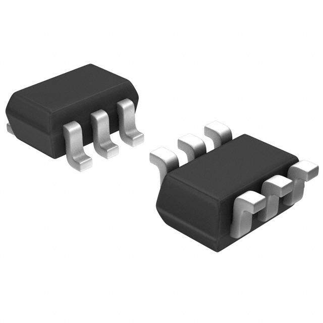
| 产品图片 |
|
| rohs | 符合RoHS无铅 / 符合限制有害物质指令(RoHS)规范要求 |
| 产品系列 | 逻辑集成电路,缓冲器和线路驱动器,ON Semiconductor MC74ACT541DTR2G74ACT |
| 数据手册 | |
| 产品型号 | MC74ACT541DTR2G |
| 产品种类 | Logic- Buffers |
| 传播延迟时间 | 7.5 ns at 5 V |
| 低电平输出电流 | 24 mA |
| 供应商器件封装 | 20-TSSOP |
| 元件数 | 1 |
| 其它名称 | MC74ACT541DTR2GOSDKR |
| 包装 | Digi-Reel® |
| 商标 | ON Semiconductor |
| 安装类型 | 表面贴装 |
| 安装风格 | SMD/SMT |
| 封装 | Reel |
| 封装/外壳 | 20-TSSOP(0.173",4.40mm 宽) |
| 封装/箱体 | TSSOP-20 |
| 工作温度 | -40°C ~ 85°C |
| 工厂包装数量 | 2500 |
| 最大功率耗散 | 200 mW |
| 最大工作温度 | + 85 C |
| 最小工作温度 | - 40 C |
| 极性 | Non-Inverting |
| 标准包装 | 1 |
| 每元件位数 | 8 |
| 每芯片的通道数量 | 8 |
| 电压-电源 | 4.5 V ~ 5.5 V |
| 电流-输出高,低 | 24mA,24mA |
| 电源电压-最大 | 5.5 V |
| 电源电压-最小 | 4.5 V |
| 系列 | MC74ACT541 |
| 输入线路数量 | 8 |
| 输出类型 | 3-State |
| 输出线路数量 | 3 |
| 逻辑类型 | CMOS |
| 逻辑系列 | ACT |
| 高电平输出电流 | - 24 mA |


- 商务部:美国ITC正式对集成电路等产品启动337调查
- 曝三星4nm工艺存在良率问题 高通将骁龙8 Gen1或转产台积电
- 太阳诱电将投资9.5亿元在常州建新厂生产MLCC 预计2023年完工
- 英特尔发布欧洲新工厂建设计划 深化IDM 2.0 战略
- 台积电先进制程称霸业界 有大客户加持明年业绩稳了
- 达到5530亿美元!SIA预计今年全球半导体销售额将创下新高
- 英特尔拟将自动驾驶子公司Mobileye上市 估值或超500亿美元
- 三星加码芯片和SET,合并消费电子和移动部门,撤换高东真等 CEO
- 三星电子宣布重大人事变动 还合并消费电子和移动部门
- 海关总署:前11个月进口集成电路产品价值2.52万亿元 增长14.8%


PDF Datasheet 数据手册内容提取
MC74AC540, MC74ACT540, MC74AC541, MC74ACT541 Octal Buffer/Line Driver with 3-State Outputs The MC74AC540/74ACT540 and MC74AC541/74ACT541 are octal buffer/line drivers designed to be employed as memory and www.onsemi.com address drivers, clock drivers and bus oriented transmitter/receivers. The MC74AC541/74ACT541 is a noninverting option of the MC74AC540/74ACT540. These devices are similar in function to the SOIC−20W MC74AC240/74ACT240 and MC74AC244/74ACT244 while DW SUFFIX CASE 751D providing flow−through architecture (inputs on opposite side from 1 outputs). This pinout arrangement makes these devices especially useful as output ports for microprocessors, allowing ease of layout and greater PC board density. TSSOP−20 Features DT SUFFIX • 3−State Outputs CASE 948E • Inputs and Outputs Opposite Side of Package, Allowing Easier 1 Interface to Microprocessors • Outputs Source/Sink 24 mA ORDERING INFORMATION • MC74AC540/74ACT540 Provides Inverted Outputs See detailed ordering and shipping information in the package • dimensions section on page 8 of this data sheet. MC74AC541/74ACT541 Provides Noninverted Outputs • ′ACT540 and ′ACT541 Have TTL Compatible Inputs DEVICE MARKING INFORMATION • These are Pb−Free Devices See general marking information in the device marking section on page 8 of this data sheet. TRUTH TABLE Inputs Outputs OE1 OE2 D ′540 ′541 L L H L H H X X Z Z X H X Z Z L L L H L H = HIGH Voltage Level L = LOW Voltage Level X = Immaterial Z = High Impedance © Semiconductor Components Industries, LLC, 2015 1 Publication Order Number: March, 2015 − Rev. 9 MC74AC540/D
MC74AC540, MC74ACT540, MC74AC541, MC74ACT541 OE1 1 20 VCC OE1 1 20 VCC 2 19 OE2 2 19 OE2 3 18 3 18 4 17 4 17 5 16 5 16 6 15 6 15 7 14 7 14 8 13 8 13 9 12 9 12 GND 10 11 GND 10 11 Figure 1. MC74AC540/74ACT540 Figure 2. MC74AC541/74ACT541 www.onsemi.com 2
MC74AC540, MC74ACT540, MC74AC541, MC74ACT541 MAXIMUM RATINGS Symbol Parameter Value Unit VCC DC Supply Voltage (Referenced to GND) −0.5 to +7.0 V VIN DC Input Voltage (Referenced to GND) −0.5 to VCC +0.5 V VOUT DC Output Voltage (Referenced to GND) (Note 1) −0.5 to VCC +0.5 V IIK DC Input Diode Current ±20 mA IOK DC Output Diode Current ±50 mA IOUT DC Output Sink/Source Current ±50 mA ICC DC Supply Current, per Output Pin ±50 mA IGND DC Ground Current, per Output Pin ±100 mA TSTG Storage Temperature Range (cid:2)65 to (cid:3)150 (cid:2)C TL Lead temperature, 1 mm from Case for 10 Seconds 260 (cid:2)C TJ Junction Temperature Under Bias 140 (cid:2)C (cid:2)JA Thermal Resistance (Note 2) SOIC 65.8 (cid:2)C/W TSSOP 110.7 MSL Moisture Sensitivity Level 1 FR Flammability Rating Oxygen Index: 30% − 35% UL 94 V−0 @ 0.125 in VESD ESD Withstand Voltage Human Body Model (Note 3) > 2000 V Machine Model (Note 4) > 200 Charged Device Model (Note 5) > 1000 ILatchup Latchup Performance Above VCC and Below GND at 85(cid:2)C (Note 6) ±100 mA Stresses exceeding those listed in the Maximum Ratings table may damage the device. If any of these limits are exceeded, device functionality should not be assumed, damage may occur and reliability may be affected. 1. IOUT absolute maximum rating must be observed. 2. The package thermal impedance is calculated in accordance with JESD 51−7. 3. Tested to EIA/JESD22−A114−A. 4. Tested to EIA/JESD22−A115−A. 5. Tested to JESD22−C101−A. 6. Tested to EIA/JESD78. RECOMMENDED OPERATING CONDITIONS Symbol Parameter Min Typ Max Unit ′AC 2.0 5.0 6.0 VCC Supply Voltage ′ACT 4.5 5.0 5.5 V VIN, VOUT DC Input Voltage, Output Voltage (Ref. to GND) 0 − VCC V VCC @ 3.0 V − 150 − Input Rise and Fall Time (Note 1) tr, tf ′AC Devices except Schmitt Inputs VCC @ 4.5 V − 40 − ns/V VCC @ 5.5 V − 25 − Input Rise and Fall Time (Note 2) VCC @ 4.5 V − 10 − tr, tf ′ACT Devices except Schmitt Inputs VCC @ 5.5 V − 8.0 − ns/V TA Operating Ambient Temperature Range −40 25 85 °C IOH Output Current − High − − −24 mA IOL Output Current − Low − − 24 mA Functional operation above the stresses listed in the Recommended Operating Ranges is not implied. Extended exposure to stresses beyond the Recommended Operating Ranges limits may affect device reliability. 1. VIN from 30% to 70% VCC; see individual Data Sheets for devices that differ from the typical input rise and fall times. 2. VIN from 0.8 V to 2.0 V; see individual Data Sheets for devices that differ from the typical input rise and fall times. www.onsemi.com 3
MC74AC540, MC74ACT540, MC74AC541, MC74ACT541 DC CHARACTERISTICS 74AC 74AC VCC TA = +25°C TA = −40°C to +85°C Symbol Parameter (V) Typ Guaranteed Limits Unit Conditions VIH Minimum High Level 3.0 1.5 2.1 2.1 VOUT = 0.1 V Input Voltage 4.5 2.25 3.15 3.15 V or VCC − 0.1 V 5.5 2.75 3.85 3.85 VIL Maximum Low Level 3.0 1.5 0.9 0.9 VOUT = 0.1 V Input Voltage 4.5 2.25 1.35 1.35 V or VCC − 0.1 V 5.5 2.75 1.65 1.65 VOH Minimum High Level 3.0 2.99 2.9 2.9 IOUT = −50 (cid:3)A Output Voltage 4.5 4.49 4.4 4.4 V 5.5 5.49 5.4 5.4 *VIN = VIL or VIH 3.0 − 2.56 2.46 −12 mA V 4.5 − 3.86 3.76 IOH −24 mA 5.5 − 4.86 4.76 −24 mA VOL Maximum Low Level 3.0 0.002 0.1 0.1 IOUT = 50 (cid:3)A Output Voltage 4.5 0.001 0.1 0.1 V 5.5 0.001 0.1 0.1 *VIN = VIL or VIH 3.0 − 0.36 0.44 12 mA V 4.5 − 0.36 0.44 IOL 24 mA 5.5 − 0.36 0.44 24 mA IIN MLeaaxkimaguem C Iunrpruetnt 5.5 − ±0.1 ±1.0 (cid:3)A VI = VCC, GND IOZ Maximum VI (OE) = VIL, VIH 3-State 5.5 − ±0.5 ±5.0 (cid:3)A VI = VCC, GND Current VO = VCC, GND IOLD †Minimum Dynamic 5.5 − − 75 mA VOLD = 1.65 V Max Output Current IOHD 5.5 − − −75 mA VOHD = 3.85 V Min ICC MSuapxpimlyu Cmu Qrreunietscent 5.5 − 8.0 80 (cid:3)A VIN = VCC or GND *All outputs loaded; thresholds on input associated with output under test. †Maximum test duration 2.0 ms, one output loaded at a time. NOTE: IIN and ICC @ 3.0 V are guaranteed to be less than or equal to the respective limit @ 5.5 V VCC. www.onsemi.com 4
MC74AC540, MC74ACT540, MC74AC541, MC74ACT541 AC CHARACTERISTICS (For Figures and Waveforms − See AND8277/D at www.onsemi.com) 74AC 74AC TA = +25°C TA = −40°C to +85°C CL = 50 pF CL = 50 pF VCC* Fig. Symbol Parameter (V) Min Typ Max Min Max Unit No. Propagation Delay 3.3 1.5 5.5 7.5 1.0 8.0 tPLH Data to Output (′AC540) 5.0 1.5 4.0 6.0 1.0 6.5 ns 3−5 Propagation Delay 3.3 1.5 5.0 7.0 1.0 7.5 tPHL Data to Output (′AC540) 5.0 1.5 4.0 5.5 1.0 6.0 ns 3−5 Output Enable Time 3.3 3.0 8.5 11 2.5 12 tPZH (′AC540) 5.0 2.0 6.5 8.5 2.0 9.5 ns 3−7 Output Enable Time 3.3 2.5 7.5 10 2.0 11 tPZL (′AC540) 5.0 2.0 6.0 7.5 1.5 8.5 ns 3−8 Output Disable Time 3.3 2.5 8.5 13 1.5 14 tPHZ (′AC540) 5.0 1.5 7.5 10.5 1.0 11 ns 3−7 Output Disable Time 3.3 2.0 7.0 10 2.0 11 tPLZ (′AC540) 5.0 1.5 6.0 8.0 1.5 9.0 ns 3−8 Propagation Delay 3.3 2.0 5.5 8.0 1.5 9.0 tPLH Data to Output (′AC541) 5.0 1.5 4.0 6.0 1.0 6.5 ns 3−5 Propagation Delay 3.3 2.0 5.5 8.0 1.5 8.5 tPHL Data to Output (′AC541) 5.0 1.5 4.0 6.0 1.0 6.5 ns 3−5 Output Enable Time 3.3 3.0 8.0 11.5 3.0 12.5 tPZH (′AC541) 5.0 2.0 6.0 8.5 1.5 9.5 ns 3−7 Output Enable Time 3.3 2.5 7.0 10 2.5 11.5 tPZL (′AC541) 5.0 1.5 5.5 7.5 1.0 8.5 ns 3−8 Output Disable Time 3.3 3.5 9.0 12.5 2.5 14 tPHZ (′AC541) 5.0 2.0 7.0 9.5 1.0 10.5 ns 3−7 Output Disable Time 3.3 2.5 6.5 9.5 2.0 10.5 tPLZ (′AC541) 5.0 2.0 5.5 7.5 1.0 8.5 ns 3−8 *Voltage Range 3.3 V is 3.3 V ±0.3 V. Voltage Range 5.0 V is 5.0 V ±0.5 V. www.onsemi.com 5
MC74AC540, MC74ACT540, MC74AC541, MC74ACT541 DC CHARACTERISTICS 74ACT 74ACT VCC TA = +25°C TA = −40°C to +85°C Symbol Parameter (V) Typ Guaranteed Limits Unit Conditions VIH Minimum High Level 4.5 1.5 2.0 2.0 V VOUT = 0.1 V Input Voltage 5.5 1.5 2.0 2.0 or VCC − 0.1 V VIL Maximum Low Level 4.5 1.5 0.8 0.8 V VOUT = 0.1 V Input Voltage 5.5 1.5 0.8 0.8 or VCC − 0.1 V VOH Minimum High Level 4.5 4.49 4.4 4.4 V IOUT = −50 (cid:3)A Output Voltage 5.5 5.49 5.4 5.4 *VIN = VIL or VIH 4.5 − 3.86 3.76 V IOH −24 mA 5.5 − 4.86 4.76 −24 mA VOL Maximum Low Level 4.5 0.001 0.1 0.1 V IOUT = 50 (cid:3)A Output Voltage 5.5 0.001 0.1 0.1 *VIN = VIL or VIH 4.5 − 0.36 0.44 V 24 mA 5.5 − 0.36 0.44 IOL 24 mA IIN MLeaaxkimaguem C Iunrpruetnt 5.5 − ±0.1 ±1.0 (cid:3)A VI = VCC, GND (cid:4)ICCT Additional Max. ICC/Input 5.5 0.6 − 1.5 mA VI = VCC −2.1 V IOZ Maximum VI (OE) = VIL, VIH 3-State 5.5 − ±0.5 ±5.0 (cid:3)A VI = VCC, GND Current VO = VCC, GND IOLD †Minimum Dynamic 5.5 − − 75 mA VOLD = 1.65 V Max Output Current IOHD 5.5 − − −75 mA VOHD = 3.85 V Min ICC MSuapxpimlyu Cmu Qrreunietscent 5.5 − 8.0 80 (cid:3)A VIN = VCC or GND *All outputs loaded; thresholds on input associated with output under test. †Maximum test duration 2.0 ms, one output loaded at a time. www.onsemi.com 6
MC74AC540, MC74ACT540, MC74AC541, MC74ACT541 AC CHARACTERISTICS (For Figures and Waveforms − See AND8277/D at www.onsemi.com) 74ACT 74ACT Symbol Parameter VCC* TA = +25°C TA = −40°C to +85°C Unit Fig. (V) CL = 50 pF CL = 50 pF No. Min Typ Max Min Max Propagation Delay tPLH Data to Output (′ACT540) 5.0 1.0 − 7.0 1.0 7.5 ns 3−5 Propagation Delay tPHL Data to Output (′ACT540) 5.0 1.0 − 8.0 1.0 8.5 ns 3−5 Output Enable Time tPZH (′ACT540) 5.0 1.0 − 10.5 1.0 11.5 ns 3−7 Output Enable Time tPZL (′ACT540) 5.0 1.0 − 9.5 1.0 10.5 ns 3−8 Output Disable Time tPHZ (′ACT540) 5.0 1.0 − 12.0 1.0 12.5 ns 3−7 Output Disable Time tPLZ (′ACT540) 5.0 1.5 − 9.0 1.0 10 ns 3−8 Propagation Delay tPLH Data to Output (′ACT541) 5.0 1.5 − 7.5 1.0 8.0 ns 3−5 Propagation Delay tPHL Data to Output (′ACT541) 5.0 1.5 − 7.5 1.0 8.0 ns 3−5 Output Enable Time tPZH (′ACT541) 5.0 2.0 − 10.0 1.0 11.0 ns 3−7 Output Enable Time tPZL (′ACT541) 5.0 1.5 − 9.5 1.0 10.5 ns 3−8 Output Disable Time tPHZ (′ACT541) 5.0 2.0 − 11.0 1.0 12.0 ns 3−7 Output Disable Time tPLZ (′ACT541) 5.0 2.0 − 9.0 1.0 10 ns 3−8 *Voltage Range 5.0 V is 5.0 V ±0.5 V. CAPACITANCE Symbol Parameter Value Typ Unit Test Conditions CIN Input Capacitance 4.5 pF VCC = 5.0 V CPD Power Dissipation Capacitance 30 pF VCC = 5.0 V www.onsemi.com 7
MC74AC540, MC74ACT540, MC74AC541, MC74ACT541 ORDERING INFORMATION Device Package Shipping† MC74AC540DWG SOIC−20 38 Units / Rail (Pb−Free) MC74AC540DWR2G SOIC−20 1000 / Tape & Reel (Pb−Free) MC74ACT540DWG SOIC−20 38 Units / Rail (Pb−Free) MC74ACT540DWR2G SOIC−20 1000 / Tape & Reel (Pb−Free) MC74ACT540DTR2G TSSOP−20 2500 / Tape & Reel (Pb−Free) MC74AC541DWG SOIC−20 38 Units / Rail (Pb−Free) MC74AC541DWR2G SOIC−20 1000 / Tape & Reel (Pb−Free) MC74ACT541DWG SOIC−20 38 Units / Rail (Pb−Free) MC74ACT541DWR2G SOIC−20 1000 / Tape & Reel (Pb−Free) MC74AC541DTR2G TSSOP−20 2500 / Tape & Reel (Pb−Free) MC74ACT541DTG TSSOP−20 75 Units / Rail (Pb−Free) MC74ACT541DTR2G TSSOP−20 2500 / Tape & Reel (Pb−Free) †For information on tape and reel specifications, including part orientation and tape sizes, please refer to our Tape and Reel Packaging Specifications Brochure, BRD8011/D. *These packages are inherently Pb−Free. MARKING DIAGRAMS SOIC−20W TSSOP−20 20 20 AC AC54x 54x AWLYYWWG ALYW(cid:3) (cid:3) 1 1 20 20 ACT ACT54x 54x AWLYYWWG ALYW(cid:3) (cid:3) 1 1 x = 0 or 1 A = Assembly Location WL, L = Wafer Lot YY, Y = Year WW, W = Work Week G or (cid:3) = Pb−Free Package (Note: Microdot may be in either location) www.onsemi.com 8
MC74AC540, MC74ACT540, MC74AC541, MC74ACT541 PACKAGE DIMENSIONS TSSOP−20 DT SUFFIX CASE 948E−02 ISSUE C NOTES: 20X K REF K 1. DIMENSIONING AND TOLERANCING PER ANSI Y14.5M, 1982. 0.15 (0.006) T U S 0.10 (0.004) M T U S V S K1 2. CONTROLLING DIMENSION: ÍÍÍÍ MILLIMETER. 3. DIMENSION A DOES NOT INCLUDE ÍÍÍÍ MOLD FLASH, PROTRUSIONS OR GATE 20 11 J J1 BURRS. MOLD FLASH OR GATE BURRS 2X L/2 ÍÍÍÍ SHALL NOT EXCEED 0.15 (0.006) PER SIDE. 4. DIMENSION B DOES NOT INCLUDE B SECTION N−N INTERLEAD FLASH OR PROTRUSION. INTERLEAD FLASH OR PROTRUSION L −U− SHALL NOT EXCEED 0.25 (0.010) PER SIDE. PIN 1 5. DIMENSION K DOES NOT INCLUDE IDENT 0.25 (0.010) DAMBAR PROTRUSION. ALLOWABLE N DAMBAR PROTRUSION SHALL BE 0.08 1 10 (0.003) TOTAL IN EXCESS OF THE K DIMENSION AT MAXIMUM MATERIAL M CONDITION. 6. TERMINAL NUMBERS ARE SHOWN FOR 0.15 (0.006) T U S REFERENCE ONLY. 7. DIMENSION A AND B ARE TO BE A DETERMINED AT DATUM PLANE −W−. N MILLIMETERS INCHES −V− F DIM MIN MAX MIN MAX A 6.40 6.60 0.252 0.260 DETAIL E B 4.30 4.50 0.169 0.177 C --- 1.20 --- 0.047 D 0.05 0.15 0.002 0.006 F 0.50 0.75 0.020 0.030 −W− G 0.65 BSC 0.026 BSC C H 0.27 0.37 0.011 0.015 J 0.09 0.20 0.004 0.008 J1 0.09 0.16 0.004 0.006 D G H K 0.19 0.30 0.007 0.012 DETAIL E K1 0.19 0.25 0.007 0.010 0.100 (0.004) ML 06 (cid:2).40 BSC8 (cid:2) 00 (cid:2).252 BSC8 (cid:2) −T− SEATING PLANE SOLDERING FOOTPRINT* 7.06 1 0.65 PITCH 16X 16X 0.36 1.26 DIMENSIONS: MILLIMETERS *For additional information on our Pb−Free strategy and soldering details, please download the ON Semiconductor Soldering and Mounting Techniques Reference Manual, SOLDERRM/D. www.onsemi.com 9
MC74AC540, MC74ACT540, MC74AC541, MC74ACT541 PACKAGE DIMENSIONS SOIC−20W DW SUFFIX CASE 751D−05 ISSUE G D NOTES: A (cid:2) 1. DIMENSIONS ARE IN MILLIMETERS. 2. INTERPRET DIMENSIONS AND TOLERANCES PER ASME Y14.5M, 1994. 3. DIMENSIONS D AND E DO NOT INCLUDE MOLD M 20 11 PROTRUSION. 4. MAXIMUM MOLD PROTRUSION 0.15 PER SIDE. B (cid:2) 5. DIMENSION B DOES NOT INCLUDE DAMBAR H M 45 PROTRUSION. ALLOWABLE PROTRUSION 10X 0.25 E hX SDCHIOMANELDNLI STBIIOEO NN0.. 1A3T TMOATXAILM IUNM E MXCATEESRSI AOLF B 1 10 MILLIMETERS DIM MIN MAX A 2.35 2.65 A1 0.10 0.25 20X B B B 0.35 0.49 C 0.23 0.32 0.25 M T A S B S D 12.65 12.95 E 7.40 7.60 e 1.27 BSC H 10.05 10.55 h 0.25 0.75 A L 0.50 0.90 (cid:2) 0 (cid:2) 7 (cid:2) L SEATING 18X e A1 TPLANE C ON Semiconductor and the are registered trademarks of Semiconductor Components Industries, LLC (SCILLC) or its subsidiaries in the United States and/or other countries. SCILLC owns the rights to a number of patents, trademarks, copyrights, trade secrets, and other intellectual property. A listing of SCILLC’s product/patent coverage may be accessed at www.onsemi.com/site/pdf/Patent−Marking.pdf. SCILLC reserves the right to make changes without further notice to any products herein. SCILLC makes no warranty, representation or guarantee regarding the suitability of its products for any particular purpose, nor does SCILLC assume any liability arising out of the application or use of any product or circuit, and specifically disclaims any and all liability, including without limitation special, consequential or incidental damages. “Typical” parameters which may be provided in SCILLC data sheets and/or specifications can and do vary in different applications and actual performance may vary over time. All operating parameters, including “Typicals” must be validated for each customer application by customer’s technical experts. SCILLC does not convey any license under its patent rights nor the rights of others. SCILLC products are not designed, intended, or authorized for use as components in systems intended for surgical implant into the body, or other applications intended to support or sustain life, or for any other application in which the failure of the SCILLC product could create a situation where personal injury or death may occur. Should Buyer purchase or use SCILLC products for any such unintended or unauthorized application, Buyer shall indemnify and hold SCILLC and its officers, employees, subsidiaries, affiliates, and distributors harmless against all claims, costs, damages, and expenses, and reasonable attorney fees arising out of, directly or indirectly, any claim of personal injury or death associated with such unintended or unauthorized use, even if such claim alleges that SCILLC was negligent regarding the design or manufacture of the part. SCILLC is an Equal Opportunity/Affirmative Action Employer. This literature is subject to all applicable copyright laws and is not for resale in any manner. PUBLICATION ORDERING INFORMATION LITERATURE FULFILLMENT: N. American Technical Support: 800−282−9855 Toll Free ON Semiconductor Website: www.onsemi.com Literature Distribution Center for ON Semiconductor USA/Canada P.O. Box 5163, Denver, Colorado 80217 USA Europe, Middle East and Africa Technical Support: Order Literature: http://www.onsemi.com/orderlit Phone: 303−675−2175 or 800−344−3860 Toll Free USA/Canada Phone: 421 33 790 2910 Fax: 303−675−2176 or 800−344−3867 Toll Free USA/Canada Japan Customer Focus Center For additional information, please contact your local Email: orderlit@onsemi.com Phone: 81−3−5817−1050 Sales Representative www.onsemi.com MC74AC540/D 10
Mouser Electronics Authorized Distributor Click to View Pricing, Inventory, Delivery & Lifecycle Information: O N Semiconductor: MC74AC540DWG MC74AC540DWR2G MC74AC541DTR2G MC74AC541DWG MC74AC541DWR2G MC74ACT540DTR2G MC74ACT540DWG MC74ACT540DWR2G MC74ACT541DTG MC74ACT541DTR2G MC74ACT541DWG MC74ACT541DWR2G