
 Datasheet下载
- 型号: MC74AC74DR2G
- 制造商: ON Semiconductor
- 库位|库存: xxxx|xxxx
- 要求:
| 数量阶梯 | 香港交货 | 国内含税 |
| +xxxx | $xxxx | ¥xxxx |
查看当月历史价格
查看今年历史价格
MC74AC74DR2G产品简介:
ICGOO电子元器件商城为您提供MC74AC74DR2G由ON Semiconductor设计生产,在icgoo商城现货销售,并且可以通过原厂、代理商等渠道进行代购。 MC74AC74DR2G价格参考¥1.11-¥1.11。ON SemiconductorMC74AC74DR2G封装/规格:逻辑 - 触发器, 。您可以下载MC74AC74DR2G参考资料、Datasheet数据手册功能说明书,资料中有MC74AC74DR2G 详细功能的应用电路图电压和使用方法及教程。
| 参数 | 数值 |
| 产品目录 | 集成电路 (IC)半导体 |
| 描述 | IC D-TYPE POS TRG DUAL 14SOIC触发器 2-6V CMOS Dual D-Type Pos. Edge |
| 产品分类 | |
| 品牌 | ON Semiconductor |
| 产品手册 | |
| 产品图片 |
|
| rohs | 符合RoHS无铅 / 符合限制有害物质指令(RoHS)规范要求 |
| 产品系列 | 逻辑集成电路,触发器,ON Semiconductor MC74AC74DR2G74AC |
| 数据手册 | |
| 产品型号 | MC74AC74DR2G |
| 不同V、最大CL时的最大传播延迟 | 10ns @ 5V,50pF |
| 产品目录页面 | |
| 产品种类 | 触发器 |
| 传播延迟时间 | 14 ns |
| 低电平输出电流 | 24 mA |
| 元件数 | 2 |
| 其它名称 | MC74AC74DR2GOSDKR |
| 功能 | 设置(预设)和复位 |
| 包装 | Digi-Reel® |
| 商标 | ON Semiconductor |
| 安装类型 | 表面贴装 |
| 安装风格 | SMD/SMT |
| 封装 | Reel |
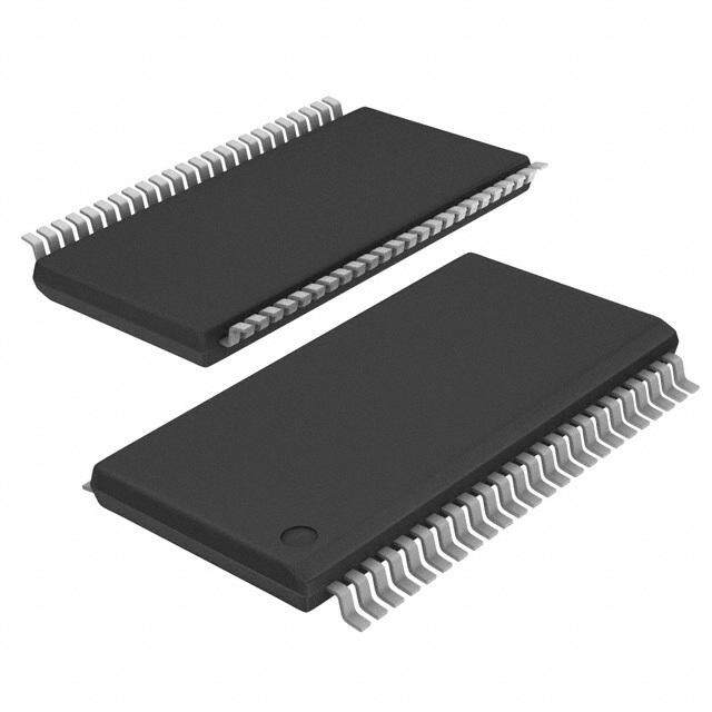
| 封装/外壳 | 14-SOIC(0.154",3.90mm 宽) |
| 封装/箱体 | SOIC-14 |
| 工作温度 | -40°C ~ 85°C (TA) |
| 工厂包装数量 | 2500 |
| 最大工作温度 | + 85 C |
| 最小工作温度 | - 40 C |
| 极性 | Inverting/Non-Inverting |
| 标准包装 | 1 |
| 每元件位数 | 1 |
| 电压-电源 | 2 V ~ 6 V |
| 电流-输出高,低 | 24mA,24mA |
| 电流-静态 | 4µA |
| 电源电压-最大 | 6 V |
| 电源电压-最小 | 2 V |
| 电路数量 | 2 |
| 类型 | D 型 |
| 系列 | MC74AC74 |
| 触发器类型 | 正边沿 |
| 输入电容 | 4.5pF |
| 输入类型 | Single-Ended |
| 输入线路数量 | 1 |
| 输出类型 | 差分 |
| 输出线路数量 | 1 |
| 逻辑类型 | D-Type Edge Triggered Flip-Flop |
| 逻辑系列 | 74AC |
| 频率-时钟 | 160MHz |
| 高电平输出电流 | - 24 mA |


PDF Datasheet 数据手册内容提取
MC74AC74, MC74ACT74 Dual D-Type Positive Edge-Triggered Flip-Flop The MC74AC74/74ACT74 is a dual D−type flip−flop with Asynchronous Clear and Set inputs and complementary (Q,Q) outputs. Information at the input is transferred to the outputs on the positive edge of the clock pulse. Clock triggering occurs at a voltage www.onsemi.com level of the clock pulse and is not directly related to the transition time of the positive-going pulse. After the Clock Pulse input threshold MARKING DIAGRAMS voltage has been passed, the Data input is locked out and information present will not be transferred to the outputs until the next rising edge 14 of the Clock Pulse input. Asynchronous Inputs: SOIC−14 xxx74G LOW input to S (Set) sets Q to HIGH level D SUFFIX AWLYWW D 14 CASE 751A LOW input to CD (Clear) sets Q to LOW level 1 Clear and Set are independent of clock 1 Simultaneous LOW on C and S makes both Q and Q HIGH D D 14 Features • xxx Outputs Source/Sink 24 mA TSSOP−14 74 • ′ACT74 Has TTL Compatible Inputs DT SUFFIX ALYW(cid:2) • 1 CASE 948G (cid:2) These are Pb−Free Devices 14 1 VCC CD2 D2 CP2 SD2 Q2 Q2 14 13 12 11 10 9 8 xxx = AC or ACT A = Assembly Location WL or L = Wafer Lot D1 CD1 Q1 CP2SD2 Q2 YWW or W== YWeoarrk Week CP1SD1 Q1 D2 CD2 Q2 G or (cid:2) = Pb−Free Package (Note: Microdot may be in either location) 1 2 3 4 5 6 7 CD1 D1 CP1 SD1 Q1 Q1 GND ORDERING INFORMATION Figure 1. Pinout: 14−Lead Packages Conductors See detailed ordering and shipping information in the package (Top View) dimensions section on page 7 of this data sheet. PIN ASSIGNMENT PIN FUNCTION D1, D2 Data Inputs CP1, CP2 Clock Pulse Inputs CD1, CD2 Direct Clear Inputs SD1, SD2 Direct Set Inputs Q1, Q1, Q2, Outputs Q2 © Semiconductor Components Industries, LLC, 2015 1 Publication Order Number: January, 2015 − Rev. 8 MC74AC74/D
MC74AC74, MC74ACT74 TRUTH TABLE (Each Half) Inputs Outputs Q1 Q1 SD CD CP D Q Q SD1 CD1 D1 CP1 L H X X H L H L X X L H L L X X H H H H H H L H H L L H H H L X Q0 Q0 Q2 Q2 SD2 CD2 NOTE: H = HIGH Voltage Level L = LOW Voltage Level D2 CP2 X = Immaterial; = LOW-to-HIGH Clock Transition Q0(Q0) = Previous Q(Q) before LOW-to-HIGH Transition of Clock Figure 2. Logic Symbol SD D Q CP Q CD NOTE: This diagram is provided only for the understanding of logic operations and should not be used to estimate propagation delays. Figure 3. Logic Diagram www.onsemi.com 2
MC74AC74, MC74ACT74 MAXIMUM RATINGS Symbol Parameter Value Unit VCC DC Supply Voltage (cid:2)0.5 to (cid:3)7.0 V VI DC Input Voltage (cid:2)0.5 (cid:4) VI (cid:4) VCC (cid:3)0.5 V VO DC Output Voltage (Note 1) (cid:2)0.5 (cid:4) VO (cid:4) VCC (cid:3)0.5 V IIK DC Input Diode Current (cid:5)20 mA IOK DC Output Diode Current (cid:5)50 mA IO DC Output Sink/Source Current (cid:5)50 mA ICC DC Supply Current per Output Pin (cid:5)50 mA IGND DC Ground Current per Output Pin (cid:5)50 mA TSTG Storage Temperature Range (cid:2)65 to (cid:3)150 °C TL Lead temperature, 1 mm from Case for 10 Seconds 260 °C TJ Junction temperature under Bias (cid:3)150 °C (cid:2) Thermal Resistance (Note 2) SOIC 125 °C/W JA TSSOP 170 PD Power Dissipation in Still Air at 85°C SOIC 125 mW TSSOP 170 MSL Moisture Sensitivity Level 1 FR Flammability Rating Oxygen Index: 30% − 35% UL 94 V−0 @ 0.125 in VESD ESD Withstand Voltage Human Body Model (Note 3) > 2000 V Machine Model (Note 4) > 200 Charged Device Model (Note 5) > 1000 ILatch−Up Latch−Up Performance Above VCC and Below GND at 85°C (Note 6) (cid:5)100 mA Stresses exceeding those listed in the Maximum Ratings table may damage the device. If any of these limits are exceeded, device functionality should not be assumed, damage may occur and reliability may be affected. 1. IO absolute maximum rating must be observed. 2. The package thermal impedance is calculated in accordance with JESD51−7. 3. Tested to EIA/JESD22−A114−A. 4. Tested to EIA/JESD22−A115−A. 5. Tested to JESD22−C101−A. 6. Tested to EIA/JESD78. RECOMMENDED OPERATING CONDITIONS Symbol Parameter Min Typ Max Unit ′AC 2.0 5.0 6.0 VCC Supply Voltage ′ACT 4.5 5.0 5.5 V Vin, Vout DC Input Voltage, Output Voltage (Ref. to GND) 0 − VCC V VCC @ 3.0 V − 150 − Input Rise and Fall Time (Note ) tr, tf ′AC Devices except Schmitt Inputs VCC @ 4.5 V − 40 − ns/V VCC @ 5.5 V − 25 − Input Rise and Fall Time (Note ) VCC @ 4.5 V − 10 − tr, tf ′ACT Devices except Schmitt Inputs VCC @ 5.5 V − 8.0 − ns/V TJ Junction Temperature (PDIP) − − 140 °C TA Operating Ambient Temperature Range −40 25 85 °C IOH Output Current − High − − −24 mA IOL Output Current − Low − − 24 mA Functional operation above the stresses listed in the Recommended Operating Ranges is not implied. Extended exposure to stresses beyond the Recommended Operating Ranges limits may affect device reliability. 1. Vin from 30% to 70% VCC; see individual Data Sheets for devices that differ from the typical input rise and fall times. 2. Vin from 0.8 V to 2.0 V; see individual Data Sheets for devices that differ from the typical input rise and fall times. www.onsemi.com 3
MC74AC74, MC74ACT74 DC CHARACTERISTICS 74AC 74AC Symbol Parameter V(VCC) TA = +25°C −4T0A°C = to Unit Conditions +85°C Typ Guaranteed Limits VIH Minimum High Level 3.0 1.5 2.1 2.1 VOUT = 0.1 V Input Voltage 4.5 2.25 3.15 3.15 V or VCC − 0.1 V 5.5 2.75 3.85 3.85 VIL Maximum Low Level 3.0 1.5 0.9 0.9 VOUT = 0.1 V Input Voltage 4.5 2.25 1.35 1.35 V or VCC − 0.1 V 5.5 2.75 1.65 1.65 VOH Minimum High Level 3.0 2.99 2.9 2.9 IOUT = −50 (cid:3)A Output Voltage 4.5 4.49 4.4 4.4 V 5.5 5.49 5.4 5.4 *VIN = VIL or VIH 3.0 − 2.56 2.46 −12 mA V 4.5 − 3.86 3.76 IOH −24 mA 5.5 − 4.86 4.76 −24 mA VOL Maximum Low Level 3.0 0.002 0.1 0.1 IOUT = 50 (cid:3)A Output Voltage 4.5 0.001 0.1 0.1 V 5.5 0.001 0.1 0.1 *VIN = VIL or VIH 3.0 − 0.36 0.44 12 mA V 4.5 − 0.36 0.44 IOL 24 mA 5.5 − 0.36 0.44 24 mA IIN MLeaaxkimaguem C Iunrpruetnt 5.5 − ±0.1 ±1.0 (cid:3)A VI = VCC, GND IOLD †Minimum Dynamic 5.5 − − 75 mA VOLD = 1.65 V Max Output Current IOHD 5.5 − − −75 mA VOHD = 3.85 V Min ICC MSuapxpimlyu Cmu Qrreunietscent 5.5 − 4.0 40 (cid:3)A VIN = VCC or GND *All outputs loaded; thresholds on input associated with output under test. †Maximum test duration 2.0 ms, one output loaded at a time. NOTE: IIN and ICC @ 3.0 V are guaranteed to be less than or equal to the respective limit @ 5.5 V VCC. AC CHARACTERISTICS 74AC 74AC Symbol Parameter VCC* TA = +25°C TtAo = + −8450°C°C Unit Fig. (V) CL = 50 pF CL = 50 pF No. Min Typ Max Min Max Maximum Clock 3.3 100 125 − 95 − fmax Frequency 5.0 140 160 − 125 − MHz 3−3 Propagation Delay 3.3 5.0 8.0 12.5 4.0 13.0 tPLH CDn or SDn to Qn or Qn 5.0 3.5 6.0 9.0 3.0 10.0 ns 3−6 Propagation Delay 3.3 4.0 10.5 12.0 3.5 13.5 tPHL CDn or SDn to Qn or Qn 5.0 3.0 8.0 9.5 2.5 10.5 ns 3−6 Propagation Delay 3.3 4.5 8.0 13.5 4.0 16.0 tPLH CPn to Qn or Qn 5.0 3.5 6.0 10.0 3.0 10.5 ns 3−6 Propagation Delay 3.3 3.5 8.0 14.0 3.5 14.5 tPHL CPn to Qn or Qn 5.0 2.5 6.0 10.0 2.5 10.5 ns 3−6 *Voltage Range 3.3 V is 3.3 V ±0.3 V. Voltage Range 5.0 V is 5.0 V ±0.5 V. www.onsemi.com 4
MC74AC74, MC74ACT74 AC OPERATING REQUIREMENTS 74AC 74AC Symbol Parameter VCC* TA = +25°C TtAo = + −8450°C°C Unit Fig. (V) CL = 50 pF CL = 50 pF No. Typ Guaranteed Minimum Set-up Time, HIGH or LOW 3.3 1.5 4.0 4.5 ts Dn to CPn 5.0 1.0 3.0 3.0 ns 3−9 Hold Time, HIGH or LOW 3.3 −2.0 0.5 0.5 th Dn to CPn 5.0 −1.5 0.5 0.5 ns 3−9 CPn or CDn or SDn 3.3 3.0 5.5 7.0 tw Pulse Width 5.0 2.5 4.5 5.0 ns 3−6 Recovery TIme 3.3 −2.5 0 0 trec CDn or SDn to CP 5.0 −2.0 0 0 ns 3−9 *Voltage Range 3.3 V is 3.3 V ±0.3 V. Voltage Range 5.0 V is 5.0 V ±0.5 V. www.onsemi.com 5
MC74AC74, MC74ACT74 DC CHARACTERISTICS 74ACT 74ACT Symbol Parameter V(VCC) TA = +25°C −4T0A°C = to Unit Conditions +85°C Typ Guaranteed Limits VIH Minimum High Level 4.5 1.5 2.0 2.0 VOUT = 0.1 V V Input Voltage 5.5 1.5 2.0 2.0 or VCC − 0.1 V VIL Maximum Low Level 4.5 1.5 0.8 0.8 VOUT = 0.1 V V Input Voltage 5.5 1.5 0.8 0.8 or VCC − 0.1 V VOH Minimum High Level 4.5 4.49 4.4 4.4 IOUT = −50 (cid:3)A V Output Voltage 5.5 5.49 5.4 5.4 *VIN = VIL or VIH 4.5 − 3.86 3.76 V −24 mA 5.5 − 4.86 4.76 IOH −24 mA VOL Maximum Low Level 4.5 0.001 0.1 0.1 IOUT = 50 (cid:3)A V Output Voltage 5.5 0.001 0.1 0.1 *VIN = VIL or VIH 4.5 − 0.36 0.44 V 24 mA 5.5 − 0.36 0.44 IOL 24 mA IIN MLeaaxkimaguem C Iunrpruetnt 5.5 − ±0.1 ±1.0 (cid:3)A VI = VCC, GND (cid:4)ICCT Additional Max. ICC/Input 5.5 0.6 − 1.5 mA VI = VCC −2.1 V IOLD †Minimum Dynamic 5.5 − − 75 mA VOLD = 1.65 V Max Output Current IOHD 5.5 − − −75 mA VOHD = 3.85 V Min ICC MSuapxpimlyu Cmu Qrreunietscent 5.5 − 4.0 40 (cid:3)A VIN = VCC or GND *All outputs loaded; thresholds on input associated with output under test. †Maximum test duration 2.0 ms, one output loaded at a time. AC CHARACTERISTICS 74ACT 74ACT Symbol Parameter VCC* TA = +25°C TtAo = + −8450°C°C Unit Fig. (V) CL = 50 pF CL = 50 pF No. Min Typ Max Min Max Maximum Clock fmax Frequency 5.0 145 210 − 125 − MHz 3−3 Propagation Delay tPLH CDn or SDn to Qn or Qn 5.0 3.0 5.5 9.5 2.5 10.5 ns 3−6 Propagation Delay tPHL CDn or SDn to Qn or Qn 5.0 3.0 6.0 10.0 3.0 11.5 ns 3−6 Propagation Delay tPLH CPn to Qn or Qn 5.0 4.0 7.5 11.0 4.0 13.0 ns 3−6 Propagation Delay tPHL CPn to Qn or Qn 5.0 3.5 6.0 10.0 3.0 11.5 ns 3−6 *Voltage Range 5.0 V is 5.0 V ±0.5 V. www.onsemi.com 6
MC74AC74, MC74ACT74 AC OPERATING REQUIREMENTS 74ACT 74ACT Symbol Parameter VCC* TA = +25°C TtAo = + −8450°C°C Unit Fig. (V) CL = 50 pF CL = 50 pF No. Typ Guaranteed Minimum Set-up Time, HIGH or LOW ts Dn to CPn 5.0 1.0 3.0 3.5 ns 3−9 Hold Time, HIGH or LOW th Dn to CPn 5.0 −0.5 1.0 1.0 ns 3−9 CPn or CDn or SDn tw Pulse Width 5.0 3.0 5.0 6.0 ns 3−6 Recovery TIme trec CDn or SDn to CP 5.0 −2.5 0 0 ns 3−9 *Voltage Range 5.0 V is 5.0 V ±0.5 V. CAPACITANCE Value Symbol Parameter Unit Test Conditions Typ CIN Input Capacitance 4.5 pF VCC = 5.0 V CPD Power Dissipation Capacitance 35 pF VCC = 5.0 V ORDERING INFORMATION Device Package Shipping† MC74AC74DG SOIC−14 55 Units/Rail (Pb−Free) MC74AC74DR2G SOIC−14 2500/Tape & Reel (Pb−Free) MC74AC74DTR2G TSSOP−14 2500/Tape & Reel (Pb−Free) MC74ACT74DG SOIC−14 55 Units/Rail (Pb−Free) MC74ACT74DR2G SOIC−14 2500/Tape & Reel (Pb−Free) MC74ACT74DTR2G TSSOP−14 2500/Tape & Reel (Pb−Free) †For information on tape and reel specifications, including part orientation and tape sizes, please refer to our Tape and Reel Packaging Specifications Brochure, BRD8011/D. www.onsemi.com 7
MC74AC74, MC74ACT74 PACKAGE DIMENSIONS SOIC−14 NB CASE 751A−03 ISSUE K D A NOTES: B 1.DIMENSIONING AND TOLERANCING PER ASME Y14.5M, 1994. 2.CONTROLLING DIMENSION: MILLIMETERS. 14 8 3.DIMENSION b DOES NOT INCLUDE DAMBAR A3 PROTRUSION. ALLOWABLE PROTRUSION SHALL BE 0.13 TOTAL IN EXCESS OF AT MAXIMUM MATERIAL CONDITION. H E 4.DIMENSIONS D AND E DO NOT INCLUDE MOLD PROTRUSIONS. L 5.MAXIMUM MOLD PROTRUSION 0.15 PER SIDE. 1 7 DETAIL A MILLIMETERS INCHES 0.25 M B M 13Xb DIM MIN MAX MIN MAX A 1.35 1.75 0.054 0.068 0.25 M C A S B S A1 0.10 0.25 0.004 0.010 A3 0.19 0.25 0.008 0.010 DETAIL A b 0.35 0.49 0.014 0.019 h A D 8.55 8.75 0.337 0.344 X 45(cid:3) E 3.80 4.00 0.150 0.157 e 1.27 BSC 0.050 BSC H 5.80 6.20 0.228 0.244 h 0.25 0.50 0.010 0.019 e A1 C SEATING M ML 0.04 0(cid:3) 1.72 5(cid:3) 0.001 6(cid:3) 0.074 9(cid:3) PLANE SOLDERING FOOTPRINT* 6.50 14X 1.18 1 1.27 PITCH 14X 0.58 DIMENSIONS: MILLIMETERS *For additional information on our Pb−Free strategy and soldering details, please download the ON Semiconductor Soldering and Mounting Techniques Reference Manual, SOLDERRM/D. www.onsemi.com 8
MC74AC74, MC74ACT74 PACKAGE DIMENSIONS TSSOP−14 CASE 948G ISSUE B 14X K REF NOTES: 1. DIMENSIONING AND TOLERANCING PER ANSI 0.10 (0.004) M T U S V S Y14.5M, 1982. 2. CONTROLLING DIMENSION: MILLIMETER. 0.15 (0.006) T U S 3. DIMENSION A DOES NOT INCLUDE MOLD FLASH, PROTRUSIONS OR GATE BURRS. N MOLD FLASH OR GATE BURRS SHALL NOT 0.25 (0.010) EXCEED 0.15 (0.006) PER SIDE. 2XL/2 14 8 4. DFLIMAESNHS OIORN P BR ODTOREUSS NIOONT. I NINCTLEURDLEE AINDT EFLRALSEHAD M OR PROTRUSION SHALL NOT EXCEED 0.25 (0.010) PER SIDE. L B 5. DIMENSION K DOES NOT INCLUDE DAMBAR −U− N PROTRUSION. ALLOWABLE DAMBAR PIN 1 PROTRUSION SHALL BE 0.08 (0.003) TOTAL IN IDENT. F EXCESS OF THE K DIMENSION AT MAXIMUM MATERIAL CONDITION. 1 7 DETAIL E 6. TERMINAL NUMBERS ARE SHOWN FOR REFERENCE ONLY. 7. DIMENSION A AND B ARE TO BE DETERMINED AT DATUM PLANE −W−. 0.15 (0.006) T U S A K MILLIMETERS INCHES −V− K1 DIM MIN MAX MIN MAX ÇÉÇÉÇÉ A 4.90 5.10 0.193 0.200 B 4.30 4.50 0.169 0.177 J J1 ÇÉÇÉÇÉ C −−− 1.20 −−− 0.047 D 0.05 0.15 0.002 0.006 F 0.50 0.75 0.020 0.030 SECTION N−N G 0.65 BSC 0.026 BSC H 0.50 0.60 0.020 0.024 J 0.09 0.20 0.004 0.008 −W− J1 0.09 0.16 0.004 0.006 C K 0.19 0.30 0.007 0.012 K1 0.19 0.25 0.007 0.010 0.10 (0.004) L 6.40 BSC 0.252 BSC M 0 (cid:3) 8 (cid:3) 0 (cid:3) 8 (cid:3) −T− SEATING D G H DETAIL E PLANE SOLDERING FOOTPRINT* 7.06 1 0.65 PITCH 14X 14X 0.36 1.26 DIMENSIONS: MILLIMETERS *For additional information on our Pb−Free strategy and soldering details, please download the ON Semiconductor Soldering and Mounting Techniques Reference Manual, SOLDERRM/D. www.onsemi.com 9
MC74AC74, MC74ACT74 ON Semiconductor and the are registered trademarks of Semiconductor Components Industries, LLC (SCILLC) or its subsidiaries in the United States and/or other countries. SCILLC owns the rights to a number of patents, trademarks, copyrights, trade secrets, and other intellectual property. A listing of SCILLC’s product/patent coverage may be accessed at www.onsemi.com/site/pdf/Patent−Marking.pdf. SCILLC reserves the right to make changes without further notice to any products herein. SCILLC makes no warranty, representation or guarantee regarding the suitability of its products for any particular purpose, nor does SCILLC assume any liability arising out of the application or use of any product or circuit, and specifically disclaims any and all liability, including without limitation special, consequential or incidental damages. “Typical” parameters which may be provided in SCILLC data sheets and/or specifications can and do vary in different applications and actual performance may vary over time. All operating parameters, including “Typicals” must be validated for each customer application by customer’s technical experts. SCILLC does not convey any license under its patent rights nor the rights of others. SCILLC products are not designed, intended, or authorized for use as components in systems intended for surgical implant into the body, or other applications intended to support or sustain life, or for any other application in which the failure of the SCILLC product could create a situation where personal injury or death may occur. Should Buyer purchase or use SCILLC products for any such unintended or unauthorized application, Buyer shall indemnify and hold SCILLC and its officers, employees, subsidiaries, affiliates, and distributors harmless against all claims, costs, damages, and expenses, and reasonable attorney fees arising out of, directly or indirectly, any claim of personal injury or death associated with such unintended or unauthorized use, even if such claim alleges that SCILLC was negligent regarding the design or manufacture of the part. SCILLC is an Equal Opportunity/Affirmative Action Employer. This literature is subject to all applicable copyright laws and is not for resale in any manner. PUBLICATION ORDERING INFORMATION LITERATURE FULFILLMENT: N. American Technical Support: 800−282−9855 Toll Free ON Semiconductor Website: www.onsemi.com Literature Distribution Center for ON Semiconductor USA/Canada P.O. Box 5163, Denver, Colorado 80217 USA Europe, Middle East and Africa Technical Support: Order Literature: http://www.onsemi.com/orderlit Phone: 303−675−2175 or 800−344−3860 Toll Free USA/Canada Phone: 421 33 790 2910 Fax: 303−675−2176 or 800−344−3867 Toll Free USA/Canada Japan Customer Focus Center For additional information, please contact your local Email: orderlit@onsemi.com Phone: 81−3−5817−1050 Sales Representative www.onsemi.com MC74AC74/D 10