ICGOO在线商城 > 集成电路(IC) > 接口 - 驱动器,接收器,收发器 > MC3486D
 Datasheet下载
- 型号: MC3486D
- 制造商: Texas Instruments
- 库位|库存: xxxx|xxxx
- 要求:
| 数量阶梯 | 香港交货 | 国内含税 |
| +xxxx | $xxxx | ¥xxxx |
查看当月历史价格
查看今年历史价格
MC3486D产品简介:
ICGOO电子元器件商城为您提供MC3486D由Texas Instruments设计生产,在icgoo商城现货销售,并且可以通过原厂、代理商等渠道进行代购。 MC3486D价格参考¥3.33-¥8.22。Texas InstrumentsMC3486D封装/规格:接口 - 驱动器,接收器,收发器, 接收器 0/4 RS422,RS423 16-SOIC。您可以下载MC3486D参考资料、Datasheet数据手册功能说明书,资料中有MC3486D 详细功能的应用电路图电压和使用方法及教程。
| 参数 | 数值 |
| 产品目录 | 集成电路 (IC)半导体 |
| 描述 | IC QUAD DIFF LINE REC 16-SOICRS-422接口集成电路 Quad Line |
| 产品分类 | |
| 品牌 | Texas Instruments |
| 产品手册 | |
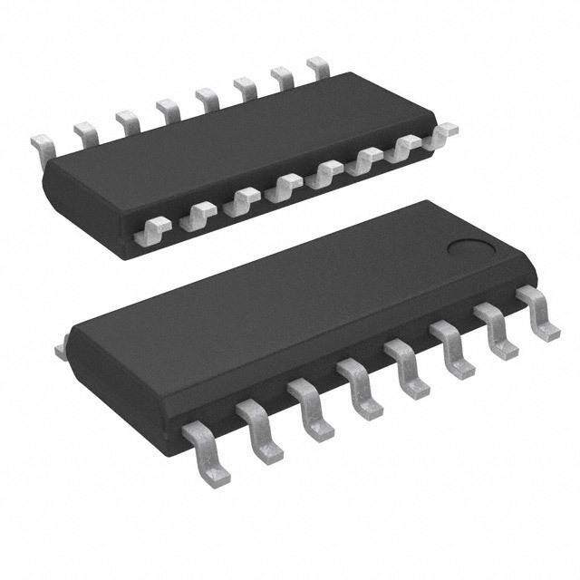
| 产品图片 |
|
| rohs | 符合RoHS无铅 / 符合限制有害物质指令(RoHS)规范要求 |
| 产品系列 | 接口 IC,RS-422接口集成电路,Texas Instruments MC3486D- |
| 数据手册 | |
| 产品型号 | MC3486D |
| 产品目录页面 | |
| 产品种类 | RS-422接口集成电路 |
| 供应商器件封装 | 16-SOIC N |
| 其它名称 | 296-7037-5 |
| 功能 | Receiver |
| 包装 | 管件 |
| 协议 | RS422,RS423 |
| 单位重量 | 141.700 mg |
| 双工 | - |
| 商标 | Texas Instruments |
| 安装类型 | 表面贴装 |
| 安装风格 | SMD/SMT |
| 封装 | Tube |
| 封装/外壳 | 16-SOIC(0.154",3.90mm 宽) |
| 封装/箱体 | SOIC-16 |
| 工作温度 | 0°C ~ 70°C |
| 工作电源电压 | 240 V |
| 工厂包装数量 | 40 |
| 接收器滞后 | - |
| 接收机数量 | 4 |
| 数据速率 | - |
| 最大工作温度 | + 70 C |
| 最小工作温度 | 0 C |
| 标准包装 | 40 |
| 电压-电源 | 4.75 V ~ 5.25 V |
| 电源电流 | 85 mA |
| 类型 | 接收器 |
| 系列 | MC3486 |
| 驱动器/接收器数 | 0/4 |


- 商务部:美国ITC正式对集成电路等产品启动337调查
- 曝三星4nm工艺存在良率问题 高通将骁龙8 Gen1或转产台积电
- 太阳诱电将投资9.5亿元在常州建新厂生产MLCC 预计2023年完工
- 英特尔发布欧洲新工厂建设计划 深化IDM 2.0 战略
- 台积电先进制程称霸业界 有大客户加持明年业绩稳了
- 达到5530亿美元!SIA预计今年全球半导体销售额将创下新高
- 英特尔拟将自动驾驶子公司Mobileye上市 估值或超500亿美元
- 三星加码芯片和SET,合并消费电子和移动部门,撤换高东真等 CEO
- 三星电子宣布重大人事变动 还合并消费电子和移动部门
- 海关总署:前11个月进口集成电路产品价值2.52万亿元 增长14.8%


PDF Datasheet 数据手册内容提取
MC3486 QUADRUPLE DIFFERENTIAL LINE RECEIVER WITH 3-STATE OUTPUTS SLLS097C – JUNE 1980 – REVISED FEBRUARY 2002 (cid:0) Meets or Exceeds the Requirements of D, N, OR NS PACKAGE ANSI Standards EIA/TIA-422-B and (TOP VIEW) EIA/TIA-423-B and ITU Recommendations V.10 and V.11 1B 1 16 VCC (cid:0) 1A 2 15 4B 3-State, TTL-Compatible Outputs (cid:0) 1Y 3 14 4A Fast Transition Times 1,2EN 4 13 4Y (cid:0) Operates From Single 5-V Supply 2Y 5 12 3,4EN (cid:0) Designed to Be Interchangeable With 2A 6 11 3Y Motorola MC3486 2B 7 10 3A GND 8 9 3B description The MC3486 is a monolithic quadruple differential line receiver designed to meet the specifications of ANSI Standards TIA/EIA-422-B and TIA/EIA-423-B and ITU Recommendations V.10 and V.11. The MC3486 offers four independent differential-input line receivers that have TTL-compatible outputs. The outputs utilize 3-state circuitry to provide a high-impedance state at any output when the appropriate output enable is at a low logic level. The MC3486 is designed for optimum performance when used with the MC3487 quadruple differential line driver. It is supplied in a 16-pin package and operates from a single 5-V supply. The MC3486 is characterized for operation from 0°C to 70°C. AVAILABLE OPTIONS PACKAGED DEVICES PLASTIC PLASTIC TA SMALL OUTLINE DIP (D, NS) (N) MC3486D 0°C to 70°C MC3486N MC3486NS The D package is available taped and reeled. Add the suffix R to the device type (e.g., MC3486DR). The NS package is only available taped and reeled. Please be aware that an important notice concerning availability, standard warranty, and use in critical applications of TexasInstruments semiconductor products and disclaimers thereto appears at the end of this data sheet. Motorola is a trademark of Motorola, Incorporated. PRODUCTION DATA information is current as of publication date. Copyright 2002, Texas Instruments Incorporated Products conform to specifications per the terms of Texas Instruments standard warranty. Production processing does not necessarily include testing of all parameters. POST OFFICE BOX 655303 • DALLAS, TEXAS 75265 1
MC3486 QUADRUPLE DIFFERENTIAL LINE RECEIVER WITH 3-STATE OUTPUTS SLLS097C – JUNE 1980 – REVISED FEBRUARY 2002 FUNCTION TABLE (each receiver) DIFFERENTIAL INPUTS OUTPUT EENNAABBLLEE A–B Y VID ≤ 0.2 V H H –0.2 V < VID < 0.2 V H ? VID ≤ –0.2 V H L Irrelevant L Z Open H ? H = high level, L = low level, Z = high impedance (off), ? = indeterminate logic diagram (positive logic) 4 1,2EN 2 1A 3 1 1Y 1B 6 2A 5 7 2Y 2B 12 3,4EN 10 3A 11 9 3Y 3B 14 4A 13 15 4Y 4B schematics of inputs and outputs EQUIVALENT OF EACH INPUT EQUIVALENT OF OUTPUT ENABLE TYPICAL OF ALL OUTPUTS EXCEPT OUTPUT ENABLE VCC VCC 8.3 kΩ 85 Ω VCC NOM NOM 16.8 kΩ 960 Ω Output 4.9 kΩ NOM NOM Enable NOM Input Output 960 Ω NOM 2 POST OFFICE BOX 655303 • DALLAS, TEXAS 75265
MC3486 QUADRUPLE DIFFERENTIAL LINE RECEIVER WITH 3-STATE OUTPUTS SLLS097C – JUNE 1980 – REVISED FEBRUARY 2002 absolute maximum ratings over operating free-air temperature range (unless otherwise noted)† Supply voltage, VCC (see Note 1) . . . . . . . . . . . . . . . . . . . . . . . . . . . . . . . . . . . . . . . . . . . . . . . . . . . . . . . . . . . . . 8 V Input voltage, VI (A or B inputs) . . . . . . . . . . . . . . . . . . . . . . . . . . . . . . . . . . . . . . . . . . . . . . . . . . . . . . . . . . . . . ±15 V Differential input voltage, V (see Note 2) . . . . . . . . . . . . . . . . . . . . . . . . . . . . . . . . . . . . . . . . . . . . . . . . . . . ±25 V ID Enable input voltage . . . . . . . . . . . . . . . . . . . . . . . . . . . . . . . . . . . . . . . . . . . . . . . . . . . . . . . . . . . . . . . . . . . . . . . . . 8 V Low-level output current, I . . . . . . . . . . . . . . . . . . . . . . . . . . . . . . . . . . . . . . . . . . . . . . . . . . . . . . . . . . . . . . 50 mA OL Package thermal impedance, θ (see Note 3): D package . . . . . . . . . . . . . . . . . . . . . . . . . . . . . . . . . . . 73°C/W JA N package . . . . . . . . . . . . . . . . . . . . . . . . . . . . . . . . . . . 67°C/W NS package . . . . . . . . . . . . . . . . . . . . . . . . . . . . . . . . . 67°C/W Lead temperature 1,6 mm (1/16 inch) from case for 10 seconds . . . . . . . . . . . . . . . . . . . . . . . . . . . . . . . 260°C Storage temperature range, T . . . . . . . . . . . . . . . . . . . . . . . . . . . . . . . . . . . . . . . . . . . . . . . . . . . –65°C to 150°C stg †Stresses beyond those listed under “absolute maximum ratings” may cause permanent damage to the device. These are stress ratings only, and functional operation of the device at these or any other conditions beyond those indicated under “recommended operating conditions” is not implied. Exposure to absolute-maximum-rated conditions for extended periods may affect device reliability. NOTES: 1. All voltage values, except differential-input voltage, are with respect to network ground terminal. 2. Differential-input voltage is measured at the noninverting input with respect to the corresponding inverting input. 3. The package thermal impedance is calculated in accordance with JESD 51-7. recommended operating conditions MIN NOM MAX UNIT VCC Supply voltage 4.75 5 5.25 V VIC Common-mode input voltage ±7 V VID Differential input voltage ±6 V VIH High-level enable input voltage 2 V VIL Low-level enable input voltage 0.8 V TA Operating free-air temperature 0 70 °C POST OFFICE BOX 655303 • DALLAS, TEXAS 75265 3
MC3486 QUADRUPLE DIFFERENTIAL LINE RECEIVER WITH 3-STATE OUTPUTS SLLS097C – JUNE 1980 – REVISED FEBRUARY 2002 electrical characteristics over recommended ranges of common-mode input voltage, supply voltage, and operating free-air temperature (unless otherwise noted) PARAMETER TEST CONDITIONS MIN MAX UNIT VIT+ Differential input high-threshold voltage VO = 2.7 V, IO = –0.4 mA 0.2 V VIT– Differential input low-threshold voltage VO = 0.5 V, IO = –8 mA –0.2† V VIK Enable-input clamp voltage II = –10 mA –1.5 V VVOOHH HHiigghh-lleevveell oouuttppuutt vvoollttaaggee VIIDD = 0.4 V,, IOO = –0.4 mA,, 22.77 VV See Note 4 and Figure 1 VVOOLL LLooww-lleevveell oouuttppuutt vvoollttaaggee VIIDD = –0.4 V,, IOO = 8 mA,, 00.55 VV See Note 4 and Figure 1 VIL = 0.8 V, VID = –3 V, VO = 2.7 V 40 IIOOZZ HHiigghh-iimmppeeddaannccee-ssttaattee oouuttppuutt ccuurrrreenntt µµAA VIL = 0.8 V, VID = 3 V, VO = 0.5 V –40 VI = –10 V –3.25 IIIIBB DDiiffffeerreennttiiaall-iinnppuutt bbiiaass ccuurrrreenntt VCCCC = 0 V or 5.25 V,, VI = –3 V –1.5 mmAA Other inputs at 0 V VI = 3 V 1.5 VI = 10 V 3.25 VI = 5.25 V 100 IIIIHH HHiigghh-lleevveell eennaabbllee iinnppuutt ccuurrrreenntt µµAA VI = 2.7 V 20 IIL Low-level enable input current VI = –0.5 V –100 µA IOS Short-circuit output current VID = 3 V, VO = 0, See Note 5 –15 –100 mA ICC Supply current VIL = 0 85 mA †The algebraic convention, in which the least positive (most negative) limit is designated as minimum, is used in this data sheet for threshold voltages only. NOTES: 4. Refer to ANSI Standards TIA/EIA-422-B and TIA/EIA-423-B for exact conditions. 5. Only one output should be shorted at a time. switching characteristics, V = 5 V, C = 15 pF, T = 25°C CC L A PARAMETER TEST CONDITIONS MIN TYP MAX UNIT tPHL Propagation delay time, high- to low-level output 28 35 ns SSeeee FFiigguurree 22 tPLH Propagation delay time, low- to high-level output 27 30 ns tPZH Output enable time to high level 13 30 ns tPZL Output enable time to low level 20 30 ns SSeeee FFiigguurree 33 tPHZ Output disable time from high level 26 35 ns tPLZ Output disable time from low level 27 35 ns 4 POST OFFICE BOX 655303 • DALLAS, TEXAS 75265
MC3486 QUADRUPLE DIFFERENTIAL LINE RECEIVER WITH 3-STATE OUTPUTS SLLS097C – JUNE 1980 – REVISED FEBRUARY 2002 PARAMETER MEASUREMENT INFORMATION 500 Ω VID 500 Ω VOH IOL IOH (+) (–) 2 V VOL Figure 1. V , V OH OL 3 V Generator Output 51 Ω (see Note A) Input 1.5 V 1.5 V 0 V CL = 15 pF tPLH tPHL (see Note B) VOH 1.5 V Output 1.3 V 1.3 V 2 V VOL TEST CIRCUIT VOLTAGE WAVEFORMS NOTES: A. The input pulse is supplied by a generator having the following characteristics: PRR ≤ 1 MHz, duty cycle = 50%, tr ≤ 6 ns, tf ≤ 6 ns. B. CL includes probe and stray capacitance. Figure 2. Test Circuit and Voltage Waveforms POST OFFICE BOX 655303 • DALLAS, TEXAS 75265 5
MC3486 QUADRUPLE DIFFERENTIAL LINE RECEIVER WITH 3-STATE OUTPUTS SLLS097C – JUNE 1980 – REVISED FEBRUARY 2002 PARAMETER MEASUREMENT INFORMATION SW1 –1.5 V Output 1.5 V SW2 2 kΩ 5 V 5 kΩ See Note C CL = 15 pF (see Note B) SW3 Generator (see Note A) 51 Ω TEST CIRCUIT 3 V 3 V tPZL tPZH SW1 to 1.5 V 1.5 V Input 1.5 V SW2 Open Input SW1 to – 1.5 V SW3 Closed 0 V 0 V SW2 Closed tPZH tPZL SW3 Open VOH 4.5 V Output Output 1.5 V 1.5 V 1.3 V VOL 3 V tPHZ 3 V SW1 to 1.5 V tPLZ SW1 to – 1.5 V Input 1.5 V SW2 Closed SW2 Closed Input SW3 Closed SW3 Closed 0 V 0 V tPHZ tPLZ 1.3 V VOH 0.5 V Output 0.5 V Output VOL 1.3 V NOTES: A. The input pulse is supplied by a generator having the following characteristics: PRR ≤ 1 MHz, duty cycle = 50%, tr ≤ 6 ns, tf ≤ 6 ns. B. CL includes probe and stray capacitance. C. All diodes are 1N916 or equivalent. Figure 3. Test Circuit and Voltage Waveforms 6 POST OFFICE BOX 655303 • DALLAS, TEXAS 75265
PACKAGE OPTION ADDENDUM www.ti.com 24-Aug-2018 PACKAGING INFORMATION Orderable Device Status Package Type Package Pins Package Eco Plan Lead/Ball Finish MSL Peak Temp Op Temp (°C) Device Marking Samples (1) Drawing Qty (2) (6) (3) (4/5) MC3486D ACTIVE SOIC D 16 40 Green (RoHS CU NIPDAU Level-1-260C-UNLIM 0 to 70 MC3486 & no Sb/Br) MC3486DE4 ACTIVE SOIC D 16 40 Green (RoHS CU NIPDAU Level-1-260C-UNLIM 0 to 70 MC3486 & no Sb/Br) MC3486DG4 ACTIVE SOIC D 16 40 Green (RoHS CU NIPDAU Level-1-260C-UNLIM 0 to 70 MC3486 & no Sb/Br) MC3486DR ACTIVE SOIC D 16 2500 Green (RoHS CU NIPDAU Level-1-260C-UNLIM 0 to 70 MC3486 & no Sb/Br) MC3486DRE4 ACTIVE SOIC D 16 2500 Green (RoHS CU NIPDAU Level-1-260C-UNLIM 0 to 70 MC3486 & no Sb/Br) MC3486N ACTIVE PDIP N 16 25 Green (RoHS CU NIPDAU N / A for Pkg Type 0 to 70 MC3486N & no Sb/Br) MC3486NE4 ACTIVE PDIP N 16 25 Green (RoHS CU NIPDAU N / A for Pkg Type 0 to 70 MC3486N & no Sb/Br) MC3486NSR ACTIVE SO NS 16 2000 Green (RoHS CU NIPDAU Level-1-260C-UNLIM 0 to 70 MC3486 & no Sb/Br) (1) The marketing status values are defined as follows: ACTIVE: Product device recommended for new designs. LIFEBUY: TI has announced that the device will be discontinued, and a lifetime-buy period is in effect. NRND: Not recommended for new designs. Device is in production to support existing customers, but TI does not recommend using this part in a new design. PREVIEW: Device has been announced but is not in production. Samples may or may not be available. OBSOLETE: TI has discontinued the production of the device. (2) RoHS: TI defines "RoHS" to mean semiconductor products that are compliant with the current EU RoHS requirements for all 10 RoHS substances, including the requirement that RoHS substance do not exceed 0.1% by weight in homogeneous materials. Where designed to be soldered at high temperatures, "RoHS" products are suitable for use in specified lead-free processes. TI may reference these types of products as "Pb-Free". RoHS Exempt: TI defines "RoHS Exempt" to mean products that contain lead but are compliant with EU RoHS pursuant to a specific EU RoHS exemption. Green: TI defines "Green" to mean the content of Chlorine (Cl) and Bromine (Br) based flame retardants meet JS709B low halogen requirements of <=1000ppm threshold. Antimony trioxide based flame retardants must also meet the <=1000ppm threshold requirement. (3) MSL, Peak Temp. - The Moisture Sensitivity Level rating according to the JEDEC industry standard classifications, and peak solder temperature. (4) There may be additional marking, which relates to the logo, the lot trace code information, or the environmental category on the device. Addendum-Page 1
PACKAGE OPTION ADDENDUM www.ti.com 24-Aug-2018 (5) Multiple Device Markings will be inside parentheses. Only one Device Marking contained in parentheses and separated by a "~" will appear on a device. If a line is indented then it is a continuation of the previous line and the two combined represent the entire Device Marking for that device. (6) Lead/Ball Finish - Orderable Devices may have multiple material finish options. Finish options are separated by a vertical ruled line. Lead/Ball Finish values may wrap to two lines if the finish value exceeds the maximum column width. Important Information and Disclaimer:The information provided on this page represents TI's knowledge and belief as of the date that it is provided. TI bases its knowledge and belief on information provided by third parties, and makes no representation or warranty as to the accuracy of such information. Efforts are underway to better integrate information from third parties. TI has taken and continues to take reasonable steps to provide representative and accurate information but may not have conducted destructive testing or chemical analysis on incoming materials and chemicals. TI and TI suppliers consider certain information to be proprietary, and thus CAS numbers and other limited information may not be available for release. In no event shall TI's liability arising out of such information exceed the total purchase price of the TI part(s) at issue in this document sold by TI to Customer on an annual basis. Addendum-Page 2
PACKAGE MATERIALS INFORMATION www.ti.com 26-Jan-2013 TAPE AND REEL INFORMATION *Alldimensionsarenominal Device Package Package Pins SPQ Reel Reel A0 B0 K0 P1 W Pin1 Type Drawing Diameter Width (mm) (mm) (mm) (mm) (mm) Quadrant (mm) W1(mm) MC3486DR SOIC D 16 2500 330.0 16.4 6.5 10.3 2.1 8.0 16.0 Q1 MC3486NSR SO NS 16 2000 330.0 16.4 8.2 10.5 2.5 12.0 16.0 Q1 PackMaterials-Page1
PACKAGE MATERIALS INFORMATION www.ti.com 26-Jan-2013 *Alldimensionsarenominal Device PackageType PackageDrawing Pins SPQ Length(mm) Width(mm) Height(mm) MC3486DR SOIC D 16 2500 333.2 345.9 28.6 MC3486NSR SO NS 16 2000 367.0 367.0 38.0 PackMaterials-Page2
None
None
None
None
IMPORTANTNOTICE TexasInstrumentsIncorporated(TI)reservestherighttomakecorrections,enhancements,improvementsandotherchangestoits semiconductorproductsandservicesperJESD46,latestissue,andtodiscontinueanyproductorserviceperJESD48,latestissue.Buyers shouldobtainthelatestrelevantinformationbeforeplacingordersandshouldverifythatsuchinformationiscurrentandcomplete. TI’spublishedtermsofsaleforsemiconductorproducts(http://www.ti.com/sc/docs/stdterms.htm)applytothesaleofpackagedintegrated circuitproductsthatTIhasqualifiedandreleasedtomarket.AdditionaltermsmayapplytotheuseorsaleofothertypesofTIproductsand services. ReproductionofsignificantportionsofTIinformationinTIdatasheetsispermissibleonlyifreproductioniswithoutalterationandis accompaniedbyallassociatedwarranties,conditions,limitations,andnotices.TIisnotresponsibleorliableforsuchreproduced documentation.Informationofthirdpartiesmaybesubjecttoadditionalrestrictions.ResaleofTIproductsorserviceswithstatements differentfromorbeyondtheparametersstatedbyTIforthatproductorservicevoidsallexpressandanyimpliedwarrantiesforthe associatedTIproductorserviceandisanunfairanddeceptivebusinesspractice.TIisnotresponsibleorliableforanysuchstatements. BuyersandotherswhoaredevelopingsystemsthatincorporateTIproducts(collectively,“Designers”)understandandagreethatDesigners remainresponsibleforusingtheirindependentanalysis,evaluationandjudgmentindesigningtheirapplicationsandthatDesignershave fullandexclusiveresponsibilitytoassurethesafetyofDesigners'applicationsandcomplianceoftheirapplications(andofallTIproducts usedinorforDesigners’applications)withallapplicableregulations,lawsandotherapplicablerequirements.Designerrepresentsthat,with respecttotheirapplications,Designerhasallthenecessaryexpertisetocreateandimplementsafeguardsthat(1)anticipatedangerous consequencesoffailures,(2)monitorfailuresandtheirconsequences,and(3)lessenthelikelihoodoffailuresthatmightcauseharmand takeappropriateactions.DesigneragreesthatpriortousingordistributinganyapplicationsthatincludeTIproducts,Designerwill thoroughlytestsuchapplicationsandthefunctionalityofsuchTIproductsasusedinsuchapplications. TI’sprovisionoftechnical,applicationorotherdesignadvice,qualitycharacterization,reliabilitydataorotherservicesorinformation, including,butnotlimitedto,referencedesignsandmaterialsrelatingtoevaluationmodules,(collectively,“TIResources”)areintendedto assistdesignerswhoaredevelopingapplicationsthatincorporateTIproducts;bydownloading,accessingorusingTIResourcesinany way,Designer(individuallyor,ifDesignerisactingonbehalfofacompany,Designer’scompany)agreestouseanyparticularTIResource solelyforthispurposeandsubjecttothetermsofthisNotice. TI’sprovisionofTIResourcesdoesnotexpandorotherwisealterTI’sapplicablepublishedwarrantiesorwarrantydisclaimersforTI products,andnoadditionalobligationsorliabilitiesarisefromTIprovidingsuchTIResources.TIreservestherighttomakecorrections, enhancements,improvementsandotherchangestoitsTIResources.TIhasnotconductedanytestingotherthanthatspecifically describedinthepublisheddocumentationforaparticularTIResource. Designerisauthorizedtouse,copyandmodifyanyindividualTIResourceonlyinconnectionwiththedevelopmentofapplicationsthat includetheTIproduct(s)identifiedinsuchTIResource.NOOTHERLICENSE,EXPRESSORIMPLIED,BYESTOPPELOROTHERWISE TOANYOTHERTIINTELLECTUALPROPERTYRIGHT,ANDNOLICENSETOANYTECHNOLOGYORINTELLECTUALPROPERTY RIGHTOFTIORANYTHIRDPARTYISGRANTEDHEREIN,includingbutnotlimitedtoanypatentright,copyright,maskworkright,or otherintellectualpropertyrightrelatingtoanycombination,machine,orprocessinwhichTIproductsorservicesareused.Information regardingorreferencingthird-partyproductsorservicesdoesnotconstitutealicensetousesuchproductsorservices,orawarrantyor endorsementthereof.UseofTIResourcesmayrequirealicensefromathirdpartyunderthepatentsorotherintellectualpropertyofthe thirdparty,oralicensefromTIunderthepatentsorotherintellectualpropertyofTI. TIRESOURCESAREPROVIDED“ASIS”ANDWITHALLFAULTS.TIDISCLAIMSALLOTHERWARRANTIESOR REPRESENTATIONS,EXPRESSORIMPLIED,REGARDINGRESOURCESORUSETHEREOF,INCLUDINGBUTNOTLIMITEDTO ACCURACYORCOMPLETENESS,TITLE,ANYEPIDEMICFAILUREWARRANTYANDANYIMPLIEDWARRANTIESOF MERCHANTABILITY,FITNESSFORAPARTICULARPURPOSE,ANDNON-INFRINGEMENTOFANYTHIRDPARTYINTELLECTUAL PROPERTYRIGHTS.TISHALLNOTBELIABLEFORANDSHALLNOTDEFENDORINDEMNIFYDESIGNERAGAINSTANYCLAIM, INCLUDINGBUTNOTLIMITEDTOANYINFRINGEMENTCLAIMTHATRELATESTOORISBASEDONANYCOMBINATIONOF PRODUCTSEVENIFDESCRIBEDINTIRESOURCESOROTHERWISE.INNOEVENTSHALLTIBELIABLEFORANYACTUAL, DIRECT,SPECIAL,COLLATERAL,INDIRECT,PUNITIVE,INCIDENTAL,CONSEQUENTIALOREXEMPLARYDAMAGESIN CONNECTIONWITHORARISINGOUTOFTIRESOURCESORUSETHEREOF,ANDREGARDLESSOFWHETHERTIHASBEEN ADVISEDOFTHEPOSSIBILITYOFSUCHDAMAGES. UnlessTIhasexplicitlydesignatedanindividualproductasmeetingtherequirementsofaparticularindustrystandard(e.g.,ISO/TS16949 andISO26262),TIisnotresponsibleforanyfailuretomeetsuchindustrystandardrequirements. WhereTIspecificallypromotesproductsasfacilitatingfunctionalsafetyorascompliantwithindustryfunctionalsafetystandards,such productsareintendedtohelpenablecustomerstodesignandcreatetheirownapplicationsthatmeetapplicablefunctionalsafetystandards andrequirements.Usingproductsinanapplicationdoesnotbyitselfestablishanysafetyfeaturesintheapplication.Designersmust ensurecompliancewithsafety-relatedrequirementsandstandardsapplicabletotheirapplications.DesignermaynotuseanyTIproductsin life-criticalmedicalequipmentunlessauthorizedofficersofthepartieshaveexecutedaspecialcontractspecificallygoverningsuchuse. Life-criticalmedicalequipmentismedicalequipmentwherefailureofsuchequipmentwouldcauseseriousbodilyinjuryordeath(e.g.,life support,pacemakers,defibrillators,heartpumps,neurostimulators,andimplantables).Suchequipmentincludes,withoutlimitation,all medicaldevicesidentifiedbytheU.S.FoodandDrugAdministrationasClassIIIdevicesandequivalentclassificationsoutsidetheU.S. TImayexpresslydesignatecertainproductsascompletingaparticularqualification(e.g.,Q100,MilitaryGrade,orEnhancedProduct). Designersagreethatithasthenecessaryexpertisetoselecttheproductwiththeappropriatequalificationdesignationfortheirapplications andthatproperproductselectionisatDesigners’ownrisk.Designersaresolelyresponsibleforcompliancewithalllegalandregulatory requirementsinconnectionwithsuchselection. DesignerwillfullyindemnifyTIanditsrepresentativesagainstanydamages,costs,losses,and/orliabilitiesarisingoutofDesigner’snon- compliancewiththetermsandprovisionsofthisNotice. MailingAddress:TexasInstruments,PostOfficeBox655303,Dallas,Texas75265 Copyright©2018,TexasInstrumentsIncorporated