ICGOO在线商城 > 集成电路(IC) > 线性 - 放大器 - 仪表,运算放大器,缓冲器放大器 > MC33202DMR2G
 Datasheet下载
- 型号: MC33202DMR2G
- 制造商: ON Semiconductor
- 库位|库存: xxxx|xxxx
- 要求:
| 数量阶梯 | 香港交货 | 国内含税 |
| +xxxx | $xxxx | ¥xxxx |
查看当月历史价格
查看今年历史价格
MC33202DMR2G产品简介:
ICGOO电子元器件商城为您提供MC33202DMR2G由ON Semiconductor设计生产,在icgoo商城现货销售,并且可以通过原厂、代理商等渠道进行代购。 MC33202DMR2G价格参考¥5.17-¥5.17。ON SemiconductorMC33202DMR2G封装/规格:线性 - 放大器 - 仪表,运算放大器,缓冲器放大器, General Purpose Amplifier 2 Circuit Rail-to-Rail Micro8™。您可以下载MC33202DMR2G参考资料、Datasheet数据手册功能说明书,资料中有MC33202DMR2G 详细功能的应用电路图电压和使用方法及教程。
| 参数 | 数值 |
| -3db带宽 | - |
| 产品目录 | 集成电路 (IC)半导体 |
| 描述 | IC OPAMP GP 2.2MHZ RRO MICRO8运算放大器 - 运放 1.8-12V Dual Rail to Rail -40 to 105 Cel |
| 产品分类 | Linear - Amplifiers - Instrumentation, OP Amps, Buffer Amps集成电路 - IC |
| 品牌 | ON Semiconductor |
| 产品手册 | |
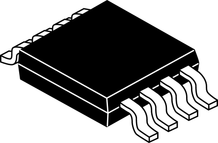
| 产品图片 |
|
| rohs | 符合RoHS无铅 / 符合限制有害物质指令(RoHS)规范要求 |
| 产品系列 | 放大器 IC,运算放大器 - 运放,ON Semiconductor MC33202DMR2G- |
| 数据手册 | |
| 产品型号 | MC33202DMR2G |
| PCN设计/规格 | |
| 产品目录页面 | |
| 产品种类 | 运算放大器 - 运放 |
| 供应商器件封装 | Micro8™ |
| 共模抑制比—最小值 | 60 dB |
| 关闭 | No Shutdown |
| 其它名称 | MC33202DMR2GOSCT |
| 包装 | 剪切带 (CT) |
| 压摆率 | 1 V/µs |
| 商标 | ON Semiconductor |
| 增益带宽生成 | 2.2 MHz |
| 增益带宽积 | 2.2MHz |
| 安装类型 | 表面贴装 |
| 安装风格 | SMD/SMT |
| 封装 | Reel |
| 封装/外壳 | 8-TSSOP,8-MSOP(0.118",3.00mm 宽) |
| 封装/箱体 | MSOP-8 |
| 工作温度 | -40°C ~ 105°C |
| 工作电源电压 | 1.8 V to 12 V, +/- 0.9 V to +/- 6 V |
| 工厂包装数量 | 4000 |
| 技术 | Bipolar |
| 放大器类型 | Low Voltage Amplifier |
| 最大双重电源电压 | +/- 6 V |
| 最大工作温度 | + 105 C |
| 最小双重电源电压 | +/- 0.9 V |
| 最小工作温度 | - 40 C |
| 标准包装 | 1 |
| 电压-电源,单/双 (±) | 1.8 V ~ 12 V, ±0.9 V ~ 6 V |
| 电压-输入失调 | 8mV |
| 电流-电源 | 900µA |
| 电流-输入偏置 | 80nA |
| 电流-输出/通道 | 80mA |
| 电源电流 | 1.8 mA |
| 电路数 | 2 |
| 系列 | MC33202 |
| 转换速度 | 1 V/us |
| 输入偏压电流—最大 | 200 nA |
| 输入参考电压噪声 | 25 nV |
| 输入补偿电压 | 8 mV |
| 输出电流 | 80 mA |
| 输出类型 | 满摆幅 |
| 通道数量 | 2 Channel |


- 商务部:美国ITC正式对集成电路等产品启动337调查
- 曝三星4nm工艺存在良率问题 高通将骁龙8 Gen1或转产台积电
- 太阳诱电将投资9.5亿元在常州建新厂生产MLCC 预计2023年完工
- 英特尔发布欧洲新工厂建设计划 深化IDM 2.0 战略
- 台积电先进制程称霸业界 有大客户加持明年业绩稳了
- 达到5530亿美元!SIA预计今年全球半导体销售额将创下新高
- 英特尔拟将自动驾驶子公司Mobileye上市 估值或超500亿美元
- 三星加码芯片和SET,合并消费电子和移动部门,撤换高东真等 CEO
- 三星电子宣布重大人事变动 还合并消费电子和移动部门
- 海关总署:前11个月进口集成电路产品价值2.52万亿元 增长14.8%


PDF Datasheet 数据手册内容提取
MC33201, MC33202, MC33204, NCV33201, NCV33202, NCV33204 Low Voltage, Rail-to-Rail Operational Amplifiers www.onsemi.com The MC33201/2/4 family of operational amplifiers provide rail−to−rail operation on both the input and output. The inputs can be driven as high as 200mV beyond the supply rails without phase reversal on the outputs, and the output can swing within 50 mV of each PDIP−8 rail. This rail−to−rail operation enables the user to make full use of the P, VP SUFFIX CASE 626 supply voltage range available. It is designed to work at very low 8 supply voltages (±0.9 V) yet can operate with a supply of up to +12V 1 and ground. Output current boosting techniques provide a high output current capability while keeping the drain current of the amplifier to a SOIC−8 minimum. Also, the combination of low noise and distortion with a 8 D, VD SUFFIX high slew rate and drive capability make this an ideal amplifier for CASE 751 1 audio applications. Features Micro8(cid:2) • DM SUFFIX Low Voltage, Single Supply Operation 8 1 CASE 846A (+1.8 V and Ground to +12 V and Ground) • Input Voltage Range Includes both Supply Rails • Output Voltage Swings within 50 mV of both Rails • No Phase Reversal on the Output for Over−driven Input Signals PDIP−14 • P, VP SUFFIX High Output Current (ISC = 80 mA, Typ) CASE 646 • Low Supply Current (I = 0.9 mA, Typ) 14 D • 600 (cid:2) Output Drive Capability 1 • Extended Operating Temperature Ranges (−40° to +105°C and −55° to +125°C) SOIC−14 D, VD SUFFIX • Typical Gain Bandwidth Product = 2.2 MHz 14 CASE 751A • 1 NCV Prefix for Automotive and Other Applications Requiring Unique Site and Control Change Requirements; AEC−Q100 Qualified and PPAP Capable TSSOP−14 • 14 DTB SUFFIX These Devices are Pb−Free and are RoHS Compliant 1 CASE 948G ORDERING INFORMATION See detailed ordering and shipping information in the package dimensions section on page 10 of this data sheet. DEVICE MARKING INFORMATION See general marking information in the device marking section on page 11 of this data sheet. © Semiconductor Components Industries, LLC, 2014 1 Publication Order Number: July, 2018 − Rev. 18 MC33201/D
MC33201, MC33202, MC33204, NCV33201, NCV33202, NCV33204 PIN CONNECTIONS MC33201 MC33204 All Case Styles All Case Styles NC 1 8 NC Output 1 1 14 Output 4 2 13 2 7 VCC Inputs 1 1 4 Inputs 4 Inputs 3 12 3 6 Output VCC 4 11 VEE VEE 4 5 NC 5 10 Inputs 2 2 3 Inputs 3 (Top View) 6 9 Output 2 7 8 Output 3 MC33202 (Top View) All Case Styles Output 1 1 8 VCC 2 7 Output 2 1 Inputs 1 3 6 Inputs 2 2 VEE 4 5 (Top View) VCC VCC VEE VCC Vin(cid:2)- Vout Vin(cid:2)+ VCC VEE This device contains 70 active transistors (each amplifier). Figure 1. Circuit Schematic (Each Amplifier) www.onsemi.com 2
MC33201, MC33202, MC33204, NCV33201, NCV33202, NCV33204 MAXIMUM RATINGS Rating Symbol Value Unit Supply Voltage (VCC to VEE) VS +13 V Input Differential Voltage Range VIDR Note 1 V Common Mode Input Voltage Range (Note 2) VCM VCC +0.5 V to V VEE −0.5 V Output Short Circuit Duration ts Note 3 sec Maximum Junction Temperature TJ +150 °C Storage Temperature Tstg −65 to +150 °C Maximum Power Dissipation PD Note 3 mW DC ELECTRICAL CHARACTERISTICS (TA = 25°C) Characteristic VCC = 2.0 V VCC = 3.3 V VCC = 5.0 V Unit Input Offset Voltage mV VIO (max) MC33201, NCV33201V ±8.0 ±8.0 ±6.0 MC33202, NCV33202, V ±10 ±10 ±8.0 MC33204, NCV33204, V ±12 ±12 ±10 Output Voltage Swing VOH (RL = 10 k(cid:2)) 1.9 3.15 4.85 Vmin VOL (RL = 10 k(cid:2)) 0.10 0.15 0.15 Vmax Power Supply Current mA per Amplifier (ID) 1.125 1.125 1.125 Specifications at VCC = 3.3 V are guaranteed by the 2.0 V and 5.0 V tests. VEE = GND. DC ELECTRICAL CHARACTERISTICS (VCC = +5.0 V, VEE = Ground, TA = 25°C, unless otherwise noted.) Characteristic Figure Symbol Min Typ Max Unit Input Offset Voltage (VCM 0 V to 0.5 V, VCM 1.0 V to 5.0 V) 3 ⎮VIO⎮ mV MC33201/NCV33201V: TA = +25°C − − 6.0 MC33201: TA = −40° to +105°C − − 9.0 MC33201V/NCV33201V: TA = −55° to +125°C − − 13 MC33202/NCV33202, V: TA = +25°C − − 8.0 MC33202/NCV33202: TA = −40° to +105°C − − 11 MC33202V/NCV33202V: TA = −55° to +125°C (Note 4) − − 14 MC33204/NCV33204V: TA = +25°C − − 10 MC33204: TA = −40° to +105°C − − 13 MC33204V/NCV33204V: TA = −55° to +125°C (Note 4) − − 17 Input Offset Voltage Temperature Coefficient (RS = 50 (cid:2)) 4 (cid:3)VIO/(cid:3)T (cid:4)V/°C TA = −40° to +105°C − 2.0 − TA = −55° to +125°C − 2.0 − Input Bias Current (VCM = 0 V to 0.5 V, VCM = 1.0 V to 5.0 V) 5, 6 ⎮IIB⎮ nA TA = +25°C − 80 200 TA = −40° to +105°C − 100 250 TA = −55° to +125°C − − 500 Stresses exceeding those listed in the Maximum Ratings table may damage the device. If any of these limits are exceeded, device functionality should not be assumed, damage may occur and reliability may be affected. 1. The differential input voltage of each amplifier is limited by two internal parallel back−to−back diodes. For additional differential input voltage range, use current limiting resistors in series with the input pins. 2. The input common mode voltage range is limited by internal diodes connected from the inputs to both supply rails. Therefore, the voltage on either input must not exceed either supply rail by more than 500 mV. 3. Power dissipation must be considered to ensure maximum junction temperature (TJ) is not exceeded. (See Figure 2) 4. All NCV devices are qualified for Automotive use. www.onsemi.com 3
MC33201, MC33202, MC33204, NCV33201, NCV33202, NCV33204 DC ELECTRICAL CHARACTERISTICS (cont.) (VCC = +5.0 V, VEE = Ground, TA = 25°C, unless otherwise noted.) Characteristic Figure Symbol Min Typ Max Unit Input Offset Current (VCM = 0 V to 0.5 V, VCM = 1.0 V to 5.0 V) − ⎮IIO⎮ nA TA = +25°C − 5.0 50 TA = −40° to +105°C − 10 100 TA = −55° to +125°C − − 200 Common Mode Input Voltage Range − VICR VEE − VCC V Large Signal Voltage Gain (VCC = +5.0 V, VEE = −5.0 V) 7 AVOL kV/V RL = 10 k(cid:2) 50 300 − RL = 600 (cid:2) 25 250 − Output Voltage Swing (VID = ±0.2 V) 8, 9, 10 V RL = 10 k(cid:2) VOH 4.85 4.95 − RL = 10 k(cid:2) VOL − 0.05 0.15 RL = 600 (cid:2) VOH 4.75 4.85 − RL = 600 (cid:2) VOL − 0.15 0.25 Common Mode Rejection (Vin = 0 V to 5.0 V) 11 CMR 60 90 − dB Power Supply Rejection Ratio 12 PSRR (cid:4)V/V VCC/VEE = 5.0 V/GND to 3.0 V/GND 500 25 − Output Short Circuit Current (Source and Sink) 13, 14 ISC 50 80 − mA Power Supply Current per Amplifier (VO = 0 V) 15 ID mA TA = −40° to +105°C − 0.9 1.125 TA = −55° to +125°C − 0.9 1.125 AC ELECTRICAL CHARACTERISTICS (VCC = +5.0 V, VEE = Ground, TA = 25°C, unless otherwise noted.) Characteristic Figure Symbol Min Typ Max Unit Slew Rate 16, 26 SR V/(cid:4)s (VS = ±2.5 V, VO = −2.0 V to +2.0 V, RL = 2.0 k(cid:2), AV = +1.0) 0.5 1.0 − Gain Bandwidth Product (f = 100 kHz) 17 GBW − 2.2 − MHz Gain Margin (RL = 600 (cid:2), CL = 0 pF) 20, 21, 22 AM − 12 − dB Phase Margin (RL = 600 (cid:2), CL = 0 pF) 20, 21, 22 (cid:2)M − 65 − Deg Channel Separation (f = 1.0 Hz to 20 kHz, AV = 100) 23 CS − 90 − dB Power Bandwidth (VO = 4.0 Vpp, RL = 600 (cid:2), THD ≤ 1 %) BWP − 28 − kHz Total Harmonic Distortion (RL = 600 (cid:2), VO = 1.0 Vpp, AV = 1.0) 24 THD % f = 1.0 kHz − 0.002 − f = 10 kHz − 0.008 − Open Loop Output Impedance ⎮ZO⎮ (cid:2) (VO = 0 V, f = 2.0 MHz, AV = 10) − 100 − Differential Input Resistance (VCM = 0 V) Rin − 200 − k(cid:2) Differential Input Capacitance (VCM = 0 V) Cin − 8.0 − pF Equivalent Input Noise Voltage (RS = 100 (cid:2)) 25 en nV/ f = 10 Hz − 25 − Hz f = 1.0 kHz − 20 − Equivalent Input Noise Current 25 in pA/ f = 10 Hz − 0.8 − Hz f = 1.0 kHz − 0.2 − www.onsemi.com 4
MC33201, MC33202, MC33204, NCV33201, NCV33202, NCV33204 W) m 2500 40 PATION ( 2000 8 and 14 Pin DIP Pkg RS (%) 35 33(cid:3)6 (0MV CaCCm3 3p=2l i+f0i(cid:2)e45r).s 0w tVeasfeter dlo tfsrom R DISSI 1500 TSSOP-14 Pkg MPLIFIE 3205 (cid:3)(cid:3)(cid:3)DVTAEIP E= P =2a 5Gc°knCadge OWE SO-14 Pkg OF A 20 UM P 1000 AGE 15 M T MAXI 500 SOPIkCg-8 RCEN 10 , x) PE 5.0 a m D( 0 0 P -(cid:2)55 -(cid:2)40 -(cid:2)25 0 25 50 85 125 -10 -(cid:2)8.0 -(cid:2)6.0 -(cid:2)4.0 -(cid:2)2.0 0 2.0 4.0 6.0 8.0 10 TA, AMBIENT TEMPERATURE (°C) VIO, INPUT OFFSET VOLTAGE (mV) Figure 2. Maximum Power Dissipation Figure 3. Input Offset Voltage Distribution versus Temperature 50 200 360 amplifiers tested from VCC = +(cid:2)5.0 V 3 (MC33204) wafer lots nA) VEE = Gnd 40 (cid:3)VCC = +(cid:2)5.0 V T (160 (cid:3)VEE = Gnd EN %) (cid:3)TA = 25°C RR OF AMPLIFIERS ( 3200 (cid:3)DIP Package , INPUT BIAS CU18200 VCM > 1.0 V VCM = 0 V to 0.5 V E 10 B40 G I A I T N E 0 0 RC -(cid:2)50 -(cid:2)40 -(cid:2)30 -(cid:2)20 -10 0 10 20 30 40 50 -(cid:2)55 -(cid:2)40 -(cid:2)25 0 25 70 85 125 E P TCVIO, INPUT OFFSET VOLTAGE TEMPERATURE COEFFICIENT ((cid:4)V/°C) TA, AMBIENT TEMPERATURE (°C) Figure 4. Input Offset Voltage Figure 5. Input Bias Current Temperature Coefficient Distribution versus Temperature 150 V) 300 V/ A) 100 N (k T (n 50 GAI 260 RREN 0 TAGE 220 U L C O AS -(cid:2)50 P V I, INPUT BIIB---(cid:2)112050000 VVTACE EC= ==2 5G1°2nC dV , OPEN LOOVOL118400 VVR(cid:3)CELV EC=O == 6= 0G+ 00(cid:2)n5. 5d(cid:2).0 V V to 4.5 V A -(cid:2)250 100 0 2.0 4.0 6.0 8.0 10 12 -(cid:2)55 -(cid:2)40 -(cid:2)25 0 25 70 85 105 125 VCM, INPUT COMMON MODE VOLTAGE (V) TA, AMBIENT TEMPERATURE (°C) Figure 6. Input Bias Current Figure 7. Open Loop Voltage Gain versus versus Common Mode Voltage Temperature www.onsemi.com 5
MC33201, MC33202, MC33204, NCV33201, NCV33202, NCV33204 12 V) VCC RL = 600 (cid:2) E ( TA = -(cid:2)55°C V)pp 10 TA = 25°C VOLTAG TA = 125°C TA = 25°C VCC - 0.2 V TAGE ( 8.0 ATION VCC - 0.4 V L 6.0 R O U V T OUTPUT 4.0 TPUT SA VVCEEC == -+(cid:2)(cid:2)55..00 VV TA = 25°C VEE + 0.4 V V,O2.0 , OUSAT TA = 125°C TA = -(cid:2)55°C VEE + 0.2 V 0 V VEE ±1.0 ±(cid:2)2.0 ±(cid:2)3.0 ±(cid:2)4.0 ±(cid:2)5.0 ±(cid:2)6.0 0 5.0 10 15 20 VCC,⎮VEE⎮ SUPPLY VOLTAGE (V) IL, LOAD CURRENT (mA) Figure 8. Output Voltage Swing Figure 9. Output Saturation Voltage versus Supply Voltage versus Load Current 12 100 B) d N ( V)pp9.0 CTIO 80 E ( JE AG RE 60 PUT VOLT 6.0 VCC = +(cid:2)6.0 V ON MODE 40 V,OUTO3.0 RATVAVEL E=== =2+6 501-°0.(cid:2)06C (cid:2).0 V MR, COMM 20 VTVACE EC= ==- (cid:2)-+5(cid:2)(cid:2)566°..0 0t o VV +125°C C 0 0 1.0 k 10 k 100 k 1.0 M 10 100 1.0 k 10 k 100 k 1.0 M f, FREQUENCY (Hz) f, FREQUENCY (Hz) Figure 10. Output Voltage Figure 11. Common Mode Rejection versus Frequency versus Frequency A) m B)120 NT (100 JECTION (d18000 PSR+ UIT CURRE 80 Source RE RC 60 PLY 60 T CI Sink P R SU PSR- HO 40 ER 40 T S W U R, PO 20 VVCEEC == -+(cid:2)(cid:2)66..00 VV OUTP 20 VVCEEC == -+(cid:2)(cid:2)66..00 VV PS TA = -(cid:2)55° to +125°C , TA = 25°C C 0 S 0 10 100 1.0 k 10 k 100 k 1.0 M I 0 1.0 2.0 3.0 4.0 5.0 6.0 f, FREQUENCY (Hz) ⎮Vout⎮, OUTPUT VOLTAGE (V) Figure 12. Power Supply Rejection Figure 13. Output Short Circuit Current versus Frequency versus Output Voltage www.onsemi.com 6
MC33201, MC33202, MC33204, NCV33201, NCV33202, NCV33204 NT (mA)150 VCC = +(cid:2)5.0 V R (mA) 2.0 CURRE125 VEE = Gnd MPLIFIE 1.6 CUIT 100 Source ER A 1.2 TA = 125°C R P OUTPUT SHORT CI 572055 Sink SUPPLY CURRENT 00..84 TA =T 2A5 =° C-(cid:2)55°C , , ISC -0(cid:2)55 -(cid:2)40 -(cid:2)25 0 25 70 85 105 125 ICC ±0(cid:2)0 ±1.0 ±(cid:2)2.0 ±(cid:2)3.0 ±(cid:2)4.0 ±(cid:2)5.0 ±(cid:2)6.0 TA, AMBIENT TEMPERATURE (°C) VCC, ⎮VEE⎮, SUPPLY VOLTAGE (V) Figure 14. Output Short Circuit Current Figure 15. Supply Current per Amplifier versus Temperature versus Supply Voltage with No Load 2.0 VCC = +(cid:2)2.5 V MHz) 4.0 VCC = +(cid:2)2.5 V μV/ s) 1.5 VVEOE = = ± -(cid:2)2(cid:2)2.0.5 V V PRODUCT ( 3.0 Vf =E E1 0=0 - k(cid:2)2H.5z V E ( +Slew Rate H AT 1.0 DT 2.0 R WI W D E -Slew Rate N L A S B R, 0.5 N 1.0 S AI G W, B G 0 0 -(cid:2)55 -(cid:2)40 -(cid:2)25 0 25 70 85 105 125 -(cid:2)55 -(cid:2)40 -(cid:2)25 0 25 70 85 105 125 TA, AMBIENT TEMPERATURE (°C) TA, AMBIENT TEMPERATURE (°C) Figure 16. Slew Rate Figure 17. Gain Bandwidth Product versus Temperature versus Temperature 70 40 70 40 E GAIN (dB) 50 VTRASL === 26±50(cid:2)6°0C. 0(cid:2) V 80 REES) E GAIN (dB) 50 RCTALL === 26050 p°0FC (cid:2) 80 REES) G G G G A E A E P VOLT 30 1A 120ASE (D P VOLT 30 2A 1A 120 ASE (D O 2A H O H O 10 160P O 10 160 P A , OPEN LVOL-10 1122AABB ---- PPGGhhaaaaiinnss,,ee CC,, LLCC LL== ==30 0 30p00 Fp 0pF FpF 1B2B 200(cid:2), EXCESS A , OPEN LVOL-10 1122AABB ---- PPGGhhaaaaiinnss,,ee VV,, SSVV SS== ==±± (cid:2)(cid:2)±±61(cid:2)(cid:2)..6100.. 00VV VV 2B 1B 200(cid:2), EXCESS -(cid:2)30 240 -(cid:2)30 240 10 k 100 k 1.0 M 10 M 10 k 100 k 1.0 M 10 M f, FREQUENCY (Hz) f, FREQUENCY (Hz) Figure 18. Voltage Gain and Phase Figure 19. Voltage Gain and Phase versus Frequency versus Frequency www.onsemi.com 7
MC33201, MC33202, MC33204, NCV33201, NCV33202, NCV33204 70 70 75 75 Phase Margin Phase Margin S) 60 60 S) E E 60 60 E E ARGIN (DEGR 543000 VVRCEL EC= ==6 0-+0(cid:2)(cid:2)66 (cid:2)..00 VV 453000 MARGIN (dB) ARGIN (DEGR 45 VTVACE EC= ==2 5-+°(cid:2)(cid:2)6C6..00 VV 45 MARGIN (dB) , PHASE MM 1200 CL = 100 pF 1200 A, GAIN M , PHASE MM3105 Gain Margin 3105 A, GAIN M (cid:2) (cid:2) Gain Margin 0 0 0 0 -(cid:2)55 -(cid:2)40 -(cid:2)25 0 25 70 85 105 125 10 100 1.0 k 10 k 100 k TA, AMBIENT TEMPERATURE (°C) RT, DIFFERENTIAL SOURCE RESISTANCE ((cid:2)) Figure 20. Gain and Phase Margin Figure 21. Gain and Phase Margin versus Temperature versus Differential Source Resistance 80 16 150 VCC = +(cid:2)6.0 V EES) 70 Phase Margin VREL E= =6 0-0(cid:2)6 (cid:2).0 V 14 dB)120 AV = 100 GR 60 AV = 100 12 B) N ( N (DE 50 Gain Margin TA = 25°C 10 GIN (d RATIO 90 E MARGI 4300 86..00 AIN MAR EL SEPA 60 AV = 10 S G N HA 20 4.0 , M AN VCC = +(cid:2)6.0 V (cid:2), PM 10 2.0 A CS, CH 30 VTVAEO E == = 28 5-.0°(cid:2)6 CV.0p pV 0 0 0 10 100 1.0 k 100 1.0 k 10 k CL, CAPACITIVE LOAD (pF) f, FREQUENCY (Hz) Figure 22. Gain and Phase Margin Figure 23. Channel Separation versus Capacitive Load versus Frequency Hz) z) STORTION (%) 11.00 VVTACO C == = 22 5+.0°(cid:2) C5V.0pp V VREL E= =6 0-0(cid:2)5 (cid:2).0 V VOLTAGE (nV/ 4500 VVTACE EC= ==2 5-+°(cid:2)(cid:2)6C6..00 VV 54..00 URRENT (pA/ H THD, TOTAL HARMONIC DI00.00.00.11110 AAAAVVVV ==== 1111.0000000 100 1.0 k 10 k 100 k e , EQUIVALENT INPUT NOISE n312100000 100 1.0 kNNooiissee VCoultraregne1t0 k 1003210 k...000 i , INPUT REFERRED NOISE Cn f, FREQUENCY (Hz) f, FREQUENCY (Hz) Figure 24. Total Harmonic Distortion Figure 25. Equivalent Input Noise Voltage versus Frequency and Current versus Frequency www.onsemi.com 8
MC33201, MC33202, MC33204, NCV33201, NCV33202, NCV33204 DETAILED OPERATING DESCRIPTION General Information Circuit Information The MC33201/2/4 family of operational amplifiers are Rail−to−rail performance is achieved at the input of the unique in their ability to swing rail−to−rail on both the input amplifiers by using parallel NPN−PNP differential input and the output with a completely bipolar design. This offers stages. When the inputs are within 800 mV of the negative low noise, high output current capability and a wide rail, the PNP stage is on. When the inputs are more than 800 common mode input voltage range even with low supply mV greater than V , the NPN stage is on. This switching of EE voltages. Operation is guaranteed over an extended input pairs will cause a reversal of input bias currents (see temperature range and at supply voltages of 2.0 V, 3.3 V and Figure 6). Also, slight differences in offset voltage may be 5.0V and ground. noted between the NPN and PNP pairs. Cross−coupling Since the common mode input voltage range extends from techniques have been used to keep this change to a minimum. V to V , it can be operated with either single or split In addition to its rail−to−rail performance, the output stage CC EE voltage supplies. The MC33201/2/4 are guaranteed not to is current boosted to provide 80 mA of output current, latch or phase reverse over the entire common mode range, enabling the op amp to drive 600 (cid:2) loads. Because of this however, the inputs should not be allowed to exceed high output current capability, care should be taken not to maximum ratings. exceed the 150°C maximum junction temperature. E (2.0 mV/DIV) VRCTVACELL EC=== ==261 500-+°00(cid:2)(cid:2)6C6 (cid:2)p..00F VV E (50 mV/DIV) VVRCTACELL EC=== ==261 500-+°00(cid:2)(cid:2)6C6 (cid:2)p..00F VV G G A A OLT OLT V V T T U U P P T T U U O O , O , O V V t, TIME (5.0 (cid:4)s/DIV) t, TIME (10 (cid:4)s/DIV) Figure 26. Noninverting Amplifier Slew Rate Figure 27. Small Signal Transient Response VCC = +(cid:2)6.0 V V/DIV) RVEL E= =6 0-0(cid:2)6 (cid:2).0 V GE (2.0 CATAVL === 2115.00°0C pF A T L O V T U P T U O , O V t, TIME (10 (cid:4)s/DIV) Figure 28. Large Signal Transient Response Surface mount board layout is a critical portion of the total between the board and the package. With the correct pad design. The footprint for the semiconductor packages must be geometry, the packages will self−align when subjected to a the correct size to ensure proper solder connection interface solder reflow process. www.onsemi.com 9
MC33201, MC33202, MC33204, NCV33201, NCV33202, NCV33204 ORDERING INFORMATION Operational Device Operating Package Shipping† Amplifier Function Temperature Range MC33201DG SOIC−8 98 Units / Rail TA= −40° to +105°C (Pb−Free) MC33201DR2G 2500 / Tape & Reel Single MC33201VDG 98 Units / Rail MC33201VDR2G TA = −55° to 125°C 2500 / Tape & Reel NCV33201VDR2G 2500 / Tape & Reel MC33202DG SOIC−8 98 Units / Rail (Pb−Free) MC33202DR2G 2500 / Tape & Reel TA= −40 ° to +105°C MC33202DMR2G Micro−8 (Pb−Free) 4000 / Tape & Reel Dual NCV33202DMR2G* MC33202VDG SOIC−8 98 Units / Rail (Pb−Free) MC33202VDR2G TA = −55° to 125°C 2500 / Tape & Reel NCV33202VDR2G* MC33204DG SO−14 55 Units / Rail (Pb−Free) MC33204DR2G 2500 Units / Tape & Reel TA= −40 ° to +105°C MC33204DTBG TSSOP−14 96 Units / Rail (Pb−Free) MC33204DTBR2G 2500 Units / Tape & Reel Quad MC33204VDG SO−14 55 Units / Rail (Pb−Free) MC33204VDR2G NCV33204DR2G* TA = −55° to 125°C 2500 Units / Tape & Reel NCV33204DTBR2G* TSSOP−14 2500 Units / Tape & Reel (Pb−Free) †For information on tape and reel specifications, including part orientation and tape sizes, please refer to our Tape and Reel Packaging Specifications Brochure, BRD8011/D. *NCV Prefix for Automotive and Other Applications Requiring Unique Site and Control Change Requirements; AEC−Q100 Qualified and PPAP Capable. www.onsemi.com 10
MC33201, MC33202, MC33204, NCV33201, NCV33202, NCV33204 MARKING DIAGRAMS SOIC−8 SOIC−8 PDIP−8 PDIP−8 Micro−8 SO−14 D SUFFIX VD SUFFIX P SUFFIX VP SUFFIX DM SUFFIX D SUFFIX CASE 751 CASE 751 CASE 626 CASE 626 CASE 846A CASE 751A 8 8 8 8 8 14 * ** 3320x 320xV MC3320xP MC33202VP 3202 AL Y(cid:2)W AL Y(cid:2)W Y Y W AWWGL Y Y W AWWGL AYW(cid:2) MACW33LY20W4WDG (cid:2) 1 1 1 1 1 1 SO−14 PDIP−14 PDIP−14 TSSOP−14 VD SUFFIX P SUFFIX VP SUFFIX DTB SUFFIX CASE 751A CASE 646 CASE 646 CASE 948G 14 14 14 14 14 * MC33204VDG MC33204P MC33204VP * AWLYWW AWLYYWWG AWLYYWWG MC33 MC33 204 204V ALYW(cid:2) ALYW(cid:2) 1 1 1 (cid:2) (cid:2) 1 1 x = 1 or 2 A = Assembly Location WL, L = Wafer Lot YY, Y = Year WW, W = Work Week G = Pb−Free Package (cid:2) = Pb−Free Package (Note: Microdot may be in either location) *This marking diagram applies to NCV3320xV **This marking diagram applies to NCV33202DMR2G www.onsemi.com 11
MC33201, MC33202, MC33204, NCV33201, NCV33202, NCV33204 PACKAGE DIMENSIONS PDIP−8 P, VP SUFFIX CASE 626−05 ISSUE N D A NOTES: 1. DIMENSIONING AND TOLERANCING PER ASME Y14.5M, 1994. E 2. CONTROLLING DIMENSION: INCHES. H 3. DIMENSIONS A, A1 AND L ARE MEASURED WITH THE PACK- AGE SEATED IN JEDEC SEATING PLANE GAUGE GS−3. 8 5 4. DIMENSIONS D, D1 AND E1 DO NOT INCLUDE MOLD FLASH OR PROTRUSIONS. MOLD FLASH OR PROTRUSIONS ARE E1 NOT TO EXCEED 0.10 INCH. 5. DIMENSION E IS MEASURED AT A POINT 0.015 BELOW DATUM 1 4 PLANE H WITH THE LEADS CONSTRAINED PERPENDICULAR TO DATUM C. 6. DIMENSION E3 IS MEASURED AT THE LEAD TIPS WITH THE NOTE 8 c LEADS UNCONSTRAINED. b2 B 7. DATUM PLANE H IS COINCIDENT WITH THE BOTTOM OF THE END VIEW LEADS, WHERE THE LEADS EXIT THE BODY. TOP VIEW WITH LEADS CONSTRAINED 8. PACKAGE CONTOUR IS OPTIONAL (ROUNDED OR SQUARE CORNERS). NOTE 5 INCHES MILLIMETERS A2 DIM MIN MAX MIN MAX e/2 A A −−−− 0.210 −−− 5.33 NOTE 3 A1 0.015 −−−− 0.38 −−− A2 0.115 0.195 2.92 4.95 L b 0.014 0.022 0.35 0.56 b2 0.060 TYP 1.52 TYP C 0.008 0.014 0.20 0.36 D 0.355 0.400 9.02 10.16 SEATING A1 PLANE D1 0.005 −−−− 0.13 −−− E 0.300 0.325 7.62 8.26 C M E1 0.240 0.280 6.10 7.11 D1 e 0.100 BSC 2.54 BSC e eB eB −−−− 0.430 −−− 10.92 L 0.115 0.150 2.92 3.81 8Xb END VIEW M −−−− 10° −−− 10° 0.010 M C A M B M NOTE 6 SIDE VIEW www.onsemi.com 12
MC33201, MC33202, MC33204, NCV33201, NCV33202, NCV33204 PACKAGE DIMENSIONS SOIC−8 NB CASE 751−07 ISSUE AK NOTES: −X− 1. DIMENSIONING AND TOLERANCING PER ANSI Y14.5M, 1982. A 2. CONTROLLING DIMENSION: MILLIMETER. 3. DIMENSION A AND B DO NOT INCLUDE MOLD PROTRUSION. 4. MAXIMUM MOLD PROTRUSION 0.15 (0.006) 8 5 PER SIDE. 5. DIMENSION D DOES NOT INCLUDE DAMBAR B S 0.25 (0.010) M Y M PROTRUSION. ALLOWABLE DAMBAR PROTRUSION SHALL BE 0.127 (0.005) TOTAL 1 IN EXCESS OF THE D DIMENSION AT −Y− 4 K 6. 7M5A1X−I0M1U TMH RMUA T7E51R−IA0L6 CAROEN DOIBTSIOONL.ETE. NEW STANDARD IS 751−07. G MILLIMETERS INCHES DIM MIN MAX MIN MAX A 4.80 5.00 0.189 0.197 C NX 45(cid:3) B 3.80 4.00 0.150 0.157 SEATING C 1.35 1.75 0.053 0.069 PLANE D 0.33 0.51 0.013 0.020 −Z− G 1.27 BSC 0.050 BSC H 0.10 0.25 0.004 0.010 0.10 (0.004) J 0.19 0.25 0.007 0.010 H D M J K 0.40 1.27 0.016 0.050 M 0 (cid:3) 8 (cid:3) 0 (cid:3) 8 (cid:3) N 0.25 0.50 0.010 0.020 0.25 (0.010)M Z Y S X S S 5.80 6.20 0.228 0.244 SOLDERING FOOTPRINT* 1.52 0.060 7.0 4.0 0.275 0.155 0.6 1.270 0.024 0.050 (cid:3) (cid:4) mm SCALE 6:1 inches *For additional information on our Pb−Free strategy and soldering details, please download the ON Semiconductor Soldering and Mounting Techniques Reference Manual, SOLDERRM/D. www.onsemi.com 13
MC33201, MC33202, MC33204, NCV33201, NCV33202, NCV33204 PACKAGE DIMENSIONS Micro8 DM SUFFIX CASE 846A−02 ISSUE H DD NOTES: 1. DIMENSIONING AND TOLERANCING PER ANSI Y14.5M, 1982. 2. CONTROLLING DIMENSION: MILLIMETER. 3. DIMENSION A DOES NOT INCLUDE MOLD FLASH, PROTRUSIONS OR GATE BURRS. MOLD FLASH, PROTRUSIONS OR GATE BURRS SHALL NOT EXCEED 0.15 (0.006) PER SIDE. HE E 4. DIMENSION B DOES NOT INCLUDE INTERLEAD FLASH OR PROTRUSION. INTERLEAD FLASH OR PROTRUSION SHALL NOT EXCEED 0.25 (0.010) PER SIDE. 5. 846A-01 OBSOLETE, NEW STANDARD 846A-02. MILLIMETERS INCHES DIM MIN NOM MAX MIN NOM MAX PIN 1 ID e A −− −− 1.10 −− −− 0.043 b8 PL A1 0.05 0.08 0.15 0.002 0.003 0.006 b 0.25 0.33 0.40 0.010 0.013 0.016 0.08 (0.003) M T B S A S c 0.13 0.18 0.23 0.005 0.007 0.009 D 2.90 3.00 3.10 0.114 0.118 0.122 E 2.90 3.00 3.10 0.114 0.118 0.122 e 0.65 BSC 0.026 BSC SEATING L 0.40 0.55 0.70 0.016 0.021 0.028 −T− PLANE HE 4.75 4.90 5.05 0.187 0.193 0.199 0.038 (0.0015) A A1 c L SOLDERING FOOTPRINT* 1.04 0.38 8X0.041 0.015 8X 3.20 4.24 5.28 0.126 0.167 0.208 0.65 (cid:3) (cid:4) 6X0.0256 SCALE 8:1 mm inches *For additional information on our Pb−Free strategy and soldering details, please download the ON Semiconductor Soldering and Mounting Techniques Reference Manual, SOLDERRM/D. www.onsemi.com 14
MC33201, MC33202, MC33204, NCV33201, NCV33202, NCV33204 PACKAGE DIMENSIONS PDIP−14 CASE 646−06 ISSUE R NOTES: 1. DIMENSIONING AND TOLERANCING PER ASME Y14.5M, 1994. D A 2. CONTROLLING DIMENSION: INCHES. 14 8 E 3. DIMENSIONS A, A1 AND L ARE MEASURED WITH THE PACK- H AGE SEATED IN JEDEC SEATING PLANE GAUGE GS−3. 4. DIMENSIONS D, D1 AND E1 DO NOT INCLUDE MOLD FLASH OR PROTRUSIONS. MOLD FLASH OR PROTRUSIONS ARE NOT TO EXCEED 0.10 INCH. E1 5. DIMENSION E IS MEASURED AT A POINT 0.015 BELOW DATUM PLANE H WITH THE LEADS CONSTRAINED PERPENDICULAR TO DATUM C. 6. DIMENSION E3 IS MEASURED AT THE LEAD TIPS WITH THE 1 7 c LEADS UNCONSTRAINED. NOTE 8 TOP VIEW b2 B WITH LEEANDSD C VOINESWTRAINED 78.. DLPEAAACTDUKSAM,G PWEL HACENORENE TH TO IHSUE RC LOISEI NAODCPSITD IEEOXNNITTA WLT H(IRTEHO B UTONHDDEY EB.DO OTTRO SMQ OUFA RTEHE NOTE 5 CORNERS). A2 INCHES MILLIMETERS A DIM MIN MAX MIN MAX NOTE 3 A −−−− 0.210 −−− 5.33 L A1 0.015 −−−− 0.38 −−− A2 0.115 0.195 2.92 4.95 b 0.014 0.022 0.35 0.56 SEATING A1 PLANE b2 0.060 TYP 1.52 TYP C 0.008 0.014 0.20 0.36 C M D 0.735 0.775 18.67 19.69 D1 D1 0.005 −−−− 0.13 −−− e eB E 0.300 0.325 7.62 8.26 14Xb END VIEW E1 0.240 0.280 6.10 7.11 e 0.100 BSC 2.54 BSC 0.010 M C A M B M NOTE 6 eB −−−− 0.430 −−− 10.92 SIDE VIEW L 0.115 0.150 2.92 3.81 M −−−− 10° −−− 10° www.onsemi.com 15
MC33201, MC33202, MC33204, NCV33201, NCV33202, NCV33204 PACKAGE DIMENSIONS SOIC−14 CASE 751A−03 ISSUE K D A NOTES: B 1.DIMENSIONING AND TOLERANCING PER ASME Y14.5M, 1994. 2.CONTROLLING DIMENSION: MILLIMETERS. 14 8 3.DIMENSION b DOES NOT INCLUDE DAMBAR A3 PROTRUSION. ALLOWABLE PROTRUSION SHALL BE 0.13 TOTAL IN EXCESS OF AT MAXIMUM MATERIAL CONDITION. H E 4.DIMENSIONS D AND E DO NOT INCLUDE MOLD PROTRUSIONS. L 5.MAXIMUM MOLD PROTRUSION 0.15 PER SIDE. 1 7 DETAIL A MILLIMETERS INCHES 0.25 M B M 13Xb DIM MIN MAX MIN MAX A 1.35 1.75 0.054 0.068 0.25 M C A S B S A1 0.10 0.25 0.004 0.010 A3 0.19 0.25 0.008 0.010 DETAIL A b 0.35 0.49 0.014 0.019 h A X 45(cid:3) DE 83..5850 84..7050 00..135307 00..135474 e 1.27 BSC 0.050 BSC H 5.80 6.20 0.228 0.244 h 0.25 0.50 0.010 0.019 e A1 C SEATING M ML 0.04 0(cid:3) 1.72 5(cid:3) 0.010 6(cid:3) 0.047 9(cid:3) PLANE SOLDERING FOOTPRINT* 6.50 14X 1.18 1 1.27 PITCH 14X 0.58 DIMENSIONS: MILLIMETERS *For additional information on our Pb−Free strategy and soldering details, please download the ON Semiconductor Soldering and Mounting Techniques Reference Manual, SOLDERRM/D. www.onsemi.com 16
MC33201, MC33202, MC33204, NCV33201, NCV33202, NCV33204 PACKAGE DIMENSIONS TSSOP−14 CASE 948G ISSUE B 14X K REF NOTES: 1. DIMENSIONING AND TOLERANCING PER 0.10 (0.004) M T U S V S ANSI Y14.5M, 1982. 2. CONTROLLING DIMENSION: MILLIMETER. 0.15 (0.006) T U S 3. DIMENSION A DOES NOT INCLUDE MOLD FLASH, PROTRUSIONS OR GATE BURRS. N MOLD FLASH OR GATE BURRS SHALL NOT 0.25 (0.010) EXCEED 0.15 (0.006) PER SIDE. 14 8 4. DIMENSION B DOES NOT INCLUDE 2XL/2 INTERLEAD FLASH OR PROTRUSION. M INTERLEAD FLASH OR PROTRUSION SHALL NOT EXCEED 0.25 (0.010) PER SIDE. L B 5. DIMENSION K DOES NOT INCLUDE −U− N DAMBAR PROTRUSION. ALLOWABLE PIN 1 DAMBAR PROTRUSION SHALL BE 0.08 IDENT. F (0.003) TOTAL IN EXCESS OF THE K DIMENSION AT MAXIMUM MATERIAL 1 7 DETAIL E CONDITION. 6. TERMINAL NUMBERS ARE SHOWN FOR REFERENCE ONLY. 7. DIMENSION A AND B ARE TO BE 0.15 (0.006) T U S A K DETERMINED AT DATUM PLANE −W−. −V− ÇÉÇÉK1ÇÉ MILLIMETERS INCHES DIM MIN MAX MIN MAX ÇÉÇÉÇÉ A 4.90 5.10 0.193 0.200 J J1 B 4.30 4.50 0.169 0.177 ÇÇÇ C −−− 1.20 −−− 0.047 SECTION N−N D 0.05 0.15 0.002 0.006 F 0.50 0.75 0.020 0.030 G 0.65 BSC 0.026 BSC H 0.50 0.60 0.020 0.024 −W− J 0.09 0.20 0.004 0.008 C J1 0.09 0.16 0.004 0.006 K 0.19 0.30 0.007 0.012 0.10 (0.004) K1 0.19 0.25 0.007 0.010 −T− SPELAATNIENG D G H DETAIL E ML 06 .(cid:3) 4 0 BS8C (cid:3) 00. 2(cid:3) 52 BS8C (cid:3) SOLDERING FOOTPRINT 7.06 1 0.65 PITCH 14X 14X 0.36 1.26 DIMENSIONS: MILLIMETERS Micro8 is a trademark of International Rectifier. ON Semiconductor and are trademarks of Semiconductor Components Industries, LLC dba ON Semiconductor or its subsidiaries in the United States and/or other countries. ON Semiconductor owns the rights to a number of patents, trademarks, copyrights, trade secrets, and other intellectual property. A listing of ON Semiconductor’s product/patent coverage may be accessed at www.onsemi.com/site/pdf/Patent−Marking.pdf. ON Semiconductor reserves the right to make changes without further notice to any products herein. ON Semiconductor makes no warranty, representation or guarantee regarding the suitability of its products for any particular purpose, nor does ON Semiconductor assume any liability arising out of the application or use of any product or circuit, and specifically disclaims any and all liability, including without limitation special, consequential or incidental damages. Buyer is responsible for its products and applications using ON Semiconductor products, including compliance with all laws, regulations and safety requirements or standards, regardless of any support or applications information provided by ON Semiconductor. “Typical” parameters which may be provided in ON Semiconductor data sheets and/or specifications can and do vary in different applications and actual performance may vary over time. All operating parameters, including “Typicals” must be validated for each customer application by customer’s technical experts. ON Semiconductor does not convey any license under its patent rights nor the rights of others. ON Semiconductor products are not designed, intended, or authorized for use as a critical component in life support systems or any FDA Class 3 medical devices or medical devices with a same or similar classification in a foreign jurisdiction or any devices intended for implantation in the human body. Should Buyer purchase or use ON Semiconductor products for any such unintended or unauthorized application, Buyer shall indemnify and hold ON Semiconductor and its officers, employees, subsidiaries, affiliates, and distributors harmless against all claims, costs, damages, and expenses, and reasonable attorney fees arising out of, directly or indirectly, any claim of personal injury or death associated with such unintended or unauthorized use, even if such claim alleges that ON Semiconductor was negligent regarding the design or manufacture of the part. ON Semiconductor is an Equal Opportunity/Affirmative Action Employer. This literature is subject to all applicable copyright laws and is not for resale in any manner. PUBLICATION ORDERING INFORMATION LITERATURE FULFILLMENT: N. American Technical Support: 800−282−9855 Toll Free ON Semiconductor Website: www.onsemi.com Literature Distribution Center for ON Semiconductor USA/Canada 19521 E. 32nd Pkwy, Aurora, Colorado 80011 USA Europe, Middle East and Africa Technical Support: Order Literature: http://www.onsemi.com/orderlit Phone: 303−675−2175 or 800−344−3860 Toll Free USA/Canada Phone: 421 33 790 2910 Fax: 303−675−2176 or 800−344−3867 Toll Free USA/Canada For additional information, please contact your local Email: orderlit@onsemi.com Sales Representative ◊ www.onsemi.com MC33201/D 17
Mouser Electronics Authorized Distributor Click to View Pricing, Inventory, Delivery & Lifecycle Information: O N Semiconductor: NCV33202VDR2G NCV33204DR2G NCV33204DTBR2G MC33201DG MC33201DR2G MC33201VDG MC33201VDR2G MC33202DG MC33202DMR2G MC33202DR2G MC33202VDG MC33202VDR2G MC33204DG MC33204DR2G MC33204DTBG MC33204DTBR2G MC33204VDG MC33204VDR2G NCV33201VDR2G SCY33202DR2G SCY33201DR2G