ICGOO在线商城 > 集成电路(IC) > 接口 - 驱动器,接收器,收发器 > MC10H116DG
 Datasheet下载
- 型号: MC10H116DG
- 制造商: ON Semiconductor
- 库位|库存: xxxx|xxxx
- 要求:
| 数量阶梯 | 香港交货 | 国内含税 |
| +xxxx | $xxxx | ¥xxxx |
查看当月历史价格
查看今年历史价格
MC10H116DG产品简介:
ICGOO电子元器件商城为您提供MC10H116DG由ON Semiconductor设计生产,在icgoo商城现货销售,并且可以通过原厂、代理商等渠道进行代购。 MC10H116DG价格参考。ON SemiconductorMC10H116DG封装/规格:接口 - 驱动器,接收器,收发器, 接收器 0/3 16-SOIC。您可以下载MC10H116DG参考资料、Datasheet数据手册功能说明书,资料中有MC10H116DG 详细功能的应用电路图电压和使用方法及教程。
| 参数 | 数值 |
| 产品目录 | 集成电路 (IC)半导体 |
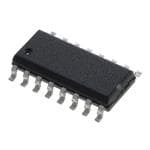
| 描述 | IC RECEIVER TRPL LINE ECL 16SOIC缓冲器和线路驱动器 Triple Diff Amplifier |
| 产品分类 | |
| 品牌 | ON Semiconductor |
| 产品手册 | |
| 产品图片 |
|
| rohs | 符合RoHS无铅 / 符合限制有害物质指令(RoHS)规范要求 |
| 产品系列 | 逻辑集成电路,缓冲器和线路驱动器,ON Semiconductor MC10H116DG10H |
| 数据手册 | |
| 产品型号 | MC10H116DG |
| 产品种类 | Logic- Receiver/Drivers |
| 供应商器件封装 | 16-SOIC |
| 其它名称 | MC10H116DGOS |
| 包装 | 管件 |
| 协议 | - |
| 双工 | - |
| 商标 | ON Semiconductor |
| 安装类型 | 表面贴装 |
| 安装风格 | SMD/SMT |
| 封装 | Tube |
| 封装/外壳 | 16-SOIC(0.154",3.90mm 宽) |
| 封装/箱体 | SO-16 |
| 工作温度 | 0°C ~ 75°C |
| 工厂包装数量 | 48 |
| 接收器滞后 | - |
| 数据速率 | - |
| 最大功率耗散 | 85 mW |
| 最大工作温度 | + 75 C |
| 最小工作温度 | 0 C |
| 标准包装 | 48 |
| 电压-电源 | 4.94 V ~ 5.46 V |
| 电源电压-最大 | - 5.46 V |
| 电源电压-最小 | - 4.94 V |
| 电源电流 | 21 mA |
| 类型 | 接收器 |
| 系列 | MC10H116 |
| 输入线路数量 | 3 |
| 逻辑类型 | Triple Line Receiver |
| 逻辑系列 | 10H |
| 驱动器/接收器数 | 0/3 |


- 商务部:美国ITC正式对集成电路等产品启动337调查
- 曝三星4nm工艺存在良率问题 高通将骁龙8 Gen1或转产台积电
- 太阳诱电将投资9.5亿元在常州建新厂生产MLCC 预计2023年完工
- 英特尔发布欧洲新工厂建设计划 深化IDM 2.0 战略
- 台积电先进制程称霸业界 有大客户加持明年业绩稳了
- 达到5530亿美元!SIA预计今年全球半导体销售额将创下新高
- 英特尔拟将自动驾驶子公司Mobileye上市 估值或超500亿美元
- 三星加码芯片和SET,合并消费电子和移动部门,撤换高东真等 CEO
- 三星电子宣布重大人事变动 还合并消费电子和移动部门
- 海关总署:前11个月进口集成电路产品价值2.52万亿元 增长14.8%


PDF Datasheet 数据手册内容提取
MC10H116 Triple Line Receiver Description The MC10H116 is a triple differential amplifier designed for use in sensing differential signals over long lines and is a functional/pinout duplication of the MC10116, with 100% improvement in propagation www.onsemi.com delay and no increase in power supply current. For termination information see AND8020. Features • Propagation Delay, 1.0ns Typical 16 20 16 • Power Dissipation 85mW Typ/Pkg (same as MECL 10K™) 1 1 1 • Improved Noise Margin 150mV (Over Operating Voltage and PDIP−16 PLCC−20 SOIC−16 Temperature Range) P SUFFIX FN SUFFIX D SUFFIX • Voltage Compensated CASE 648−08 CASE 775−02 CASE 751B−05 • MECL 10K Compatible • These Devices are Pb-Free, Halogen Free and are RoHS Compliant MARKING DIAGRAMS* 4 2 *VBB to be used to supply bias to the MC10H116 only and bypassed 5 3 (when used) with 0.01(cid:2)(cid:3)F to 0.1(cid:3)F capacitor to ground (0V). VBB can source < 1.0mA. 120 9 6 The MC10H116 is designed to be used in sensing differential signals 16 16 10 7 odveevric leo nugs elifnuel sa.s T ah eS cbhiamsi tst utrpigpglye (rV, oBrB i)n i so tmheard ea papvlaicialatbiolen st ow mhearkee a the MC10H116P 10H116G 12 14 stable reference voltage is necessary. AWLYYWWG 10H116G AWLYWW Active current sources provide these receivers with excellent 1 AWLYYWW 1 13 15 common−mode noise rejection. If any amplifier in a package is not 11 used, one input of that amplifier must be connected to VBB to prevent VBB* unbalancing the current−source bias network. The MC10H116 does not have internal−input pull− down resistors. VCC1 = Pin 1 This provides high impedance to the amplifier input and facilitates A = Assembly Location VCC2 = Pin 16 differential connections. WL = Wafer Lot VEE = Pin 8 • ALopwpl iLceavtieoln Rs:eceiver •Voltage Level YY = Year When input pin with • Schmitt Trigger Interface WW = Work Week bubble goes positive it’s respective output pin with bubble goes positive. *For additional marking information, refer to Application Note AND8002/D. Figure 1. Logic Diagram ORDERING INFORMATION Device Package Shipping† VCC1 1 16 VCC2 MC10H116DG SOIC−16 48 Units/Tube AOUT 2 15 COUT (Pb-Free) AOUT 3 14 COUT MC10H116DR2G SOIC−16 2500/Tape & Reel AIN 4 13 CIN (Pb-Free) AIN 5 12 CIN MC10H116FNG PLCC−20 46 Units/Tube BOUT 6 11 VBB (Pb-Free) BOUT 7 10 BIN MC10H116FNR2G PLCC−20 500/Tape & Reel (Pb-Free) VEE 8 9 BIN MC10H116PG PDIP−16 25 Units/Tube Pin assignment is for Dual−in−Line Package. (Pb-Free) For PLCC pin assignment, see TND309, the Pin Conversion Tables, page 9. †For information on tape and reel specifications, in- cluding part orientation and tape sizes, please refer Figure 2. Dip Pin Assignment to our Tape and Reel Packaging Specifications Brochure, BRD8011/D. © Semiconductor Components Industries, LLC, 2016 1 Publication Order Number: August, 2016 − Rev. 11 MC10H116/D
MC10H116 Table 1. MAXIMUM RATINGS Symbol Characteristic Rating Unit VEE Power Supply (VCC = 0) −8.0 to 0 Vdc VI Input Voltage (VCC = 0) 0 to VEE Vdc Iout Output Current mA Continuous 50 Surge 100 TA Operating Temperature Range 0 to +75 °C Tstg Storage Temperature Range °C Plastic −55 to +150 Ceramic −55 to +165 Stresses exceeding those listed in the Maximum Ratings table may damage the device. If any of these limits are exceeded, device functionality should not be assumed, damage may occur and reliability may be affected. Table 2. ELECTRICAL CHARACTERISTICS (VEE = −5.2 V ±5%) (Note 2) 0° 25° 75° Symbol Characteristic Min Max Min Max Min Max Unit IE Power Supply Current − 23 − 21 − 23 mA IinH Input Current High − 150 − 95 − 95 (cid:3)A ICBO Input Leakage Current − 1.5 − 1.0 − 1.0 (cid:3)A VBB Reference Voltage −1.38 −1.27 −1.35 −1.25 −1.31 −1.19 Vdc VOH High Output Voltage −1.02 −0.84 −0.98 −0.81 −0.92 −0.735 Vdc VOL Low Output Voltage −1.95 −1.63 −1.95 −1.63 −1.95 −1.60 Vdc VIH High Input Voltage (Note 1) −1.17 −0.84 −1.13 −0.81 −1.07 −0.735 Vdc VIL Low Input Voltage (Note 1) −1.95 −1.48 −1.95 −1.48 −1.95 −1.45 Vdc VCMR Common Mode Range (Note 4) − − −2.85 to −0.8 − − Vdc VPP Input Sensitivity (Note 3) − − 150 typ − − mVPP 1. When VBB is used as the reference voltage. 2. Each MECL 10H™ series circuit has been designed to meet the specifications shown in the test table, after thermal equilibrium has been established. The circuit is in a test socket or mounted on a printed circuit board and transverse air flow greater than 500lfpm is maintained. Outputs are terminated through a 50ohm resistor to −2.0 V. 3. Differential input not to exceed 1.0Vdc. 4. 150mVp−p differential input required to obtain full logic swing on output. Table 3. AC CHARACTERISTICS 0° 25° 75° Symbol Characteristic Min Max Min Max Min Max Unit tpd Propagation Delay 0.4 1.3 0.4 1.3 0.45 1.45 ns tr Rise Time 0.5 1.5 0.5 1.6 0.5 1.7 ns tf Fall Time 0.5 1.5 0.5 1.6 0.5 1.7 ns NOTE:Device will meet the specifications after thermal equilibrium has been established when mounted in a test socket or printed circuit board with maintained transverse airflow greater than 500lfpm. Electrical parameters are guaranteed only over the declared operating temperature range. Functional operation of the device exceeding these conditions is not implied. Device specification limit values are applied individually under normal operating conditions and not valid simultaneously. www.onsemi.com 2
MC10H116 PACKAGE DIMENSIONS 20 LEAD PLLC CASE 775−02 ISSUE F B 0.007 (0.180) M T L-M S N S −N− Y BRK U 0.007 (0.180) M T L-M S N S D −L− −M− Z W D 20 1 X G1 0.010 (0.250) S T L-M S N S V VIEW D−D A 0.007 (0.180) M T L-M S N S Z R 0.007 (0.180) M T L-M S N S H 0.007 (0.180) M T L-M S N S C E K1 0.004 (0.100) K G J −T− SEATING PLANE F 0.007 (0.180) M T L-M S N S VIEW S G1 VIEW S 0.010 (0.250) S T L-M S N S NOTES: 1. DIMENSIONS AND TOLERANCING PER ANSI Y14.5M, INCHES MILLIMETERS 1982. DIM MIN MAX MIN MAX 2. DIMENSIONS IN INCHES. A 0.385 0.395 9.78 10.03 3. DATUMS −L−, −M−, AND −N− DETERMINED WHERE TOP OF LEAD SHOULDER EXITS PLASTIC BODY AT MOLD B 0.385 0.395 9.78 10.03 PARTING LINE. C 0.165 0.180 4.20 4.57 4. DIMENSION G1, TRUE POSITION TO BE MEASURED AT E 0.090 0.110 2.29 2.79 DATUM −T−, SEATING PLANE. F 0.013 0.021 0.33 0.53 5. DIMENSIONS R AND U DO NOT INCLUDE MOLD FLASH. G 0.050 BSC 1.27 BSC ALLOWABLE MOLD FLASH IS 0.010 (0.250) PER SIDE. H 0.026 0.032 0.66 0.81 6. DIMENSIONS IN THE PACKAGE TOP MAY BE SMALLER J 0.020 −−− 0.51 −−− THAN THE PACKAGE BOTTOM BY UP TO 0.012 (0.300). K 0.025 −−− 0.64 −−− DIMENSIONS R AND U ARE DETERMINED AT THE R 0.350 0.356 8.89 9.04 OUTERMOST EXTREMES OF THE PLASTIC BODY U 0.350 0.356 8.89 9.04 EXCLUSIVE OF MOLD FLASH, TIE BAR BURRS, GATE V 0.042 0.048 1.07 1.21 BURRS AND INTERLEAD FLASH, BUT INCLUDING ANY W 0.042 0.048 1.07 1.21 MISMATCH BETWEEN THE TOP AND BOTTOM OF THE X 0.042 0.056 1.07 1.42 PLASTIC BODY. 7. DPRIMOETNRSUIOSINO NH ODOR EINST NROUTS IIONCNL. U TDHEE DDAAMMBBAARR YZ −2− −(cid:2) 0.1002 0(cid:2) −−2 −(cid:2) 01.05 0(cid:2) PROTRUSION(S) SHALL NOT CAUSE THE H DIMENSION G1 0.310 0.330 7.88 8.38 TO BE GREATER THAN 0.037 (0.940). THE DAMBAR K1 0.040 −−− 1.02 −−− INTRUSION(S) SHALL NOT CAUSE THE H DIMENSION TO BE SMALLER THAN 0.025 (0.635). www.onsemi.com 3
MC10H116 PACKAGE DIMENSIONS SOIC−16 CASE 751B−05 ISSUE K −A− NOTES: 1. DIMENSIONING AND TOLERANCING PER ANSI Y14.5M, 1982. 2. CONTROLLING DIMENSION: MILLIMETER. 16 9 3. DIMENSIONS A AND B DO NOT INCLUDE MOLD PROTRUSION. 4. MAXIMUM MOLD PROTRUSION 0.15 (0.006) PER SIDE. −B− P8 PL 5. DIMENSION D DOES NOT INCLUDE DAMBAR PROTRUSION. ALLOWABLE DAMBAR PROTRUSION 1 8 0.25 (0.010) M B S SHALL BE 0.127 (0.005) TOTAL IN EXCESS OF THE D DIMENSION AT MAXIMUM MATERIAL CONDITION. MILLIMETERS INCHES DIM MIN MAX MIN MAX G A 9.80 10.00 0.386 0.393 B 3.80 4.00 0.150 0.157 C 1.35 1.75 0.054 0.068 D 0.35 0.49 0.014 0.019 F K R X 45(cid:2) F 0.40 1.25 0.016 0.049 G 1.27 BSC 0.050 BSC J 0.19 0.25 0.008 0.009 C K 0.10 0.25 0.004 0.009 M 0 (cid:2) 7 (cid:2) 0 (cid:2) 7 (cid:2) −T− SEATING P 5.80 6.20 0.229 0.244 PLANE M J R 0.25 0.50 0.010 0.019 D 16 PL 0.25 (0.010) M T B S A S SOLDERING FOOTPRINT STYLE 1: STYLE 2: STYLE 3: STYLE 4: PIN 1. COLLECTOR PIN 1. CATHODE PIN 1. COLLECTOR, DYE #1 PIN 1. COLLECTOR, DYE #1 8X 2. BASE 2. ANODE 2. BASE, #1 2. COLLECTOR, #1 6.40 3. EMITTER 3. NO CONNECTION 3. EMITTER, #1 3. COLLECTOR, #2 4. NO CONNECTION 4. CATHODE 4. COLLECTOR, #1 4. COLLECTOR, #2 16X1.12 5. EMITTER 5. CATHODE 5. COLLECTOR, #2 5. COLLECTOR, #3 6. BASE 6. NO CONNECTION 6. BASE, #2 6. COLLECTOR, #3 1 16 7. COLLECTOR 7. ANODE 7. EMITTER, #2 7. COLLECTOR, #4 8. COLLECTOR 8. CATHODE 8. COLLECTOR, #2 8. COLLECTOR, #4 9. BASE 9. CATHODE 9. COLLECTOR, #3 9. BASE, #4 10. EMITTER 10. ANODE 10. BASE, #3 10. EMITTER, #4 16X 11. NO CONNECTION 11. NO CONNECTION 11. EMITTER, #3 11. BASE, #3 0.58 12. EMITTER 12. CATHODE 12. COLLECTOR, #3 12. EMITTER, #3 13. BASE 13. CATHODE 13. COLLECTOR, #4 13. BASE, #2 14. COLLECTOR 14. NO CONNECTION 14. BASE, #4 14. EMITTER, #2 15. EMITTER 15. ANODE 15. EMITTER, #4 15. BASE, #1 16. COLLECTOR 16. CATHODE 16. COLLECTOR, #4 16. EMITTER, #1 1.27 STYLE 5: STYLE 6: STYLE 7: PITCH PIN 1. DRAIN, DYE #1 PIN 1. CATHODE PIN 1. SOURCE N‐CH 2. DRAIN, #1 2. CATHODE 2. COMMON DRAIN (OUTPUT) 3. DRAIN, #2 3. CATHODE 3. COMMON DRAIN (OUTPUT) 8 9 4. DRAIN, #2 4. CATHODE 4. GATE P‐CH 5. DRAIN, #3 5. CATHODE 5. COMMON DRAIN (OUTPUT) 6. DRAIN, #3 6. CATHODE 6. COMMON DRAIN (OUTPUT) DIMENSIONS: MILLIMETERS 7. DRAIN, #4 7. CATHODE 7. COMMON DRAIN (OUTPUT) 8. DRAIN, #4 8. CATHODE 8. SOURCE P‐CH *For additional information on our Pb-Free 9. GATE, #4 9. ANODE 9. SOURCE P‐CH strategy and soldering details, please 10. SOURCE, #4 10. ANODE 10. COMMON DRAIN (OUTPUT) download the ON Semiconductor Soldering 11. GATE, #3 11. ANODE 11. COMMON DRAIN (OUTPUT) 12. SOURCE, #3 12. ANODE 12. COMMON DRAIN (OUTPUT) and Mounting Techniques Reference Man- 13. GATE, #2 13. ANODE 13. GATE N‐CH ual, SOLDERRM/D. 14. SOURCE, #2 14. ANODE 14. COMMON DRAIN (OUTPUT) 15. GATE, #1 15. ANODE 15. COMMON DRAIN (OUTPUT) 16. SOURCE, #1 16. ANODE 16. SOURCE N‐CH www.onsemi.com 4
MC10H116 PACKAGE DIMENSIONS PDIP−16 CASE 648−08 ISSUE V NOTES: 1. DIMENSIONING AND TOLERANCING PER ASME Y14.5M, 1994. D A 2. CONTROLLING DIMENSION: INCHES. 16 9 E 3. DIMENSIONS A, A1 AND L ARE MEASURED WITH THE PACK- H AGE SEATED IN JEDEC SEATING PLANE GAUGE GS−3. 4. DIMENSIONS D, D1 AND E1 DO NOT INCLUDE MOLD FLASH OR PROTRUSIONS. MOLD FLASH OR PROTRUSIONS ARE NOT TO EXCEED 0.10 INCH. E1 5. DIMENSION E IS MEASURED AT A POINT 0.015 BELOW DATUM PLANE H WITH THE LEADS CONSTRAINED PERPENDICULAR TO DATUM C. 6. DIMENSION eB IS MEASURED AT THE LEAD TIPS WITH THE 1 8 c LEADS UNCONSTRAINED. NOTE 8 TOP VIEW b2 B WITH LEEANDSD C VOINESWTRAINED 78.. DLPEAAACTDUKSAM,G PWEL HACENORENE TH TO IHSUE RC LOISEI NAODCPSITD IEEOXNNITTA WLT H(IRTEHO B UTONHDDEY EB.DO OTTRO SMQ OUFA RTEHE NOTE 5 CORNERS). A2 e/2 A INCHES MILLIMETERS DIM MIN MAX MIN MAX NOTE 3 A −−−− 0.210 −−− 5.33 L A1 0.015 −−−− 0.38 −−− A2 0.115 0.195 2.92 4.95 b 0.014 0.022 0.35 0.56 b2 0.060 TYP 1.52 TYP A1 C SPELAATNIENG M CD 00..070385 00..071745 108.2.607 109.3.669 D1 D1 0.005 −−−− 0.13 −−− e eB E 0.300 0.325 7.62 8.26 16Xb END VIEW E1 0.240 0.280 6.10 7.11 e 0.100 BSC 2.54 BSC 0.010 M C A M B M NOTE 6 eB −−−− 0.430 −−− 10.92 SIDE VIEW L 0.115 0.150 2.92 3.81 M −−−− 10° −−− 10° STYLE 1: STYLE 2: PIN 1. CATHODE PIN 1. COMMON DRAIN 2. CATHODE 2. COMMON DRAIN 3. CATHODE 3. COMMON DRAIN 4. CATHODE 4. COMMON DRAIN 5. CATHODE 5. COMMON DRAIN 6. CATHODE 6. COMMON DRAIN 7. CATHODE 7. COMMON DRAIN 8. CATHODE 8. COMMON DRAIN 9. ANODE 9. GATE 10. ANODE 10. SOURCE 11. ANODE 11. GATE 12. ANODE 12. SOURCE 13. ANODE 13. GATE 14. ANODE 14. SOURCE 15. ANODE 15. GATE 16. ANODE 16. SOURCE MECL is a trademark of Semiconductor Components Industries, LLC (SCILLC) or its subsidiaries in the United States and/or other countries. ON Semiconductor and are trademarks of Semiconductor Components Industries, LLC dba ON Semiconductor or its subsidiaries in the United States and/or other countries. ON Semiconductor owns the rights to a number of patents, trademarks, copyrights, trade secrets, and other intellectual property. A listing of ON Semiconductor’s product/patent coverage may be accessed at www.onsemi.com/site/pdf/Patent-Marking.pdf. ON Semiconductor reserves the right to make changes without further notice to any products herein. ON Semiconductor makes no warranty, representation or guarantee regarding the suitability of its products for any particular purpose, nor does ON Semiconductor assume any liability arising out of the application or use of any product or circuit, and specifically disclaims any and all liability, including without limitation special, consequential or incidental damages. Buyer is responsible for its products and applications using ON Semiconductor products, including compliance with all laws, regulations and safety requirements or standards, regardless of any support or applications information provided by ON Semiconductor. “Typical” parameters which may be provided in ON Semiconductor data sheets and/or specifications can and do vary in different applications and actual performance may vary over time. All operating parameters, including “Typicals” must be validated for each customer application by customer’s technical experts. ON Semiconductor does not convey any license under its patent rights nor the rights of others. ON Semiconductor products are not designed, intended, or authorized for use as a critical component in life support systems or any FDA Class 3 medical devices or medical devices with a same or similar classification in a foreign jurisdiction or any devices intended for implantation in the human body. Should Buyer purchase or use ON Semiconductor products for any such unintended or unauthorized application, Buyer shall indemnify and hold ON Semiconductor and its officers, employees, subsidiaries, affiliates, and distributors harmless against all claims, costs, damages, and expenses, and reasonable attorney fees arising out of, directly or indirectly, any claim of personal injury or death associated with such unintended or unauthorized use, even if such claim alleges that ON Semiconductor was negligent regarding the design or manufacture of the part. ON Semiconductor is an Equal Opportunity/Affirmative Action Employer. This literature is subject to all applicable copyright laws and is not for resale in any manner. PUBLICATION ORDERING INFORMATION LITERATURE FULFILLMENT: N. American Technical Support: 800−282−9855 Toll Free ON Semiconductor Website: www.onsemi.com Literature Distribution Center for ON Semiconductor USA/Canada 19521 E. 32nd Pkwy, Aurora, Colorado 80011 USA Europe, Middle East and Africa Technical Support: Order Literature: http://www.onsemi.com/orderlit Phone: 303−675−2175 or 800−344−3860 Toll Free USA/Canada Phone: 421 33 790 2910 Fax: 303−675−2176 or 800−344−3867 Toll Free USA/Canada Japan Customer Focus Center For additional information, please contact your local Email: orderlit@onsemi.com Phone: 81−3−5817−1050 Sales Representative www.onsemi.com MC10H116/D 5