ICGOO在线商城 > 集成电路(IC) > 逻辑器件 - 转换器,电平移位器 > MC100LVEL90DWG

 Datasheet下载
- 型号: MC100LVEL90DWG
- 制造商: ON Semiconductor
- 库位|库存: xxxx|xxxx
- 要求:
| 数量阶梯 | 香港交货 | 国内含税 |
| +xxxx | $xxxx | ¥xxxx |
查看当月历史价格
查看今年历史价格
MC100LVEL90DWG产品简介:
ICGOO电子元器件商城为您提供MC100LVEL90DWG由ON Semiconductor设计生产,在icgoo商城现货销售,并且可以通过原厂、代理商等渠道进行代购。 MC100LVEL90DWG价格参考。ON SemiconductorMC100LVEL90DWG封装/规格:逻辑器件 - 转换器,电平移位器, Mixed Signal Translator Unidirectional 1 Circuit 3 Channel 20-SOIC。您可以下载MC100LVEL90DWG参考资料、Datasheet数据手册功能说明书,资料中有MC100LVEL90DWG 详细功能的应用电路图电压和使用方法及教程。
| 参数 | 数值 |
| 产品目录 | 集成电路 (IC)半导体 |
| 描述 | IC XLATOR TRPL ECL-LVPECL 20SOIC转换 - 电压电平 -3.3V/-5V Triple ECL to LVPECL |
| 产品分类 | 逻辑 - 变换器集成电路 - IC |
| 品牌 | ON Semiconductor |
| 产品手册 | |
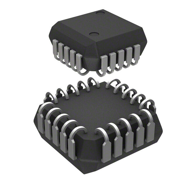
| 产品图片 |
|
| rohs | 符合RoHS无铅 / 符合限制有害物质指令(RoHS)规范要求 |
| 产品系列 | 逻辑集成电路,转换 - 电压电平,ON Semiconductor MC100LVEL90DWG100LVEL |
| 数据手册 | |
| 产品型号 | MC100LVEL90DWG |
| 产品种类 | 转换 - 电压电平 |
| 传播延迟时间 | 0.67 ns |
| 传播延迟(最大值) | 0.67ns |
| 位数 | 3 |
| 供应商器件封装 | 20-SOIC |
| 其它名称 | MC100LVEL90DWGOS |
| 包装 | 管件 |
| 商标 | ON Semiconductor |
| 安装类型 | 表面贴装 |
| 安装风格 | SMD/SMT |
| 封装 | Tube |
| 封装/外壳 | 20-SOIC(0.295",7.50mm 宽) |
| 封装/箱体 | SOIC-20 Wide |
| 工作温度 | -40°C ~ 85°C |
| 工厂包装数量 | 38 |
| 差分-输入:输出 | 无/无 |
| 数据速率 | - |
| 最大工作温度 | + 85 C |
| 最小工作温度 | - 40 C |
| 标准包装 | 38 |
| 电压-电源 | 3 V ~ 3.8 V |
| 电源电压-最大 | - 5.5 V, + 3.8 V |
| 电源电压-最小 | - 3 V |
| 类型 | ECL to LVPECL |
| 系列 | MC100LVEL90 |
| 输入类型 | ECL |
| 输出/通道数 | 1 |
| 输出类型 | LVPECL |
| 通道数 | 3 |
| 逻辑功能 | 变换器 |
| 零件号别名 | MC100LVEL59DWG |


- 商务部:美国ITC正式对集成电路等产品启动337调查
- 曝三星4nm工艺存在良率问题 高通将骁龙8 Gen1或转产台积电
- 太阳诱电将投资9.5亿元在常州建新厂生产MLCC 预计2023年完工
- 英特尔发布欧洲新工厂建设计划 深化IDM 2.0 战略
- 台积电先进制程称霸业界 有大客户加持明年业绩稳了
- 达到5530亿美元!SIA预计今年全球半导体销售额将创下新高
- 英特尔拟将自动驾驶子公司Mobileye上市 估值或超500亿美元
- 三星加码芯片和SET,合并消费电子和移动部门,撤换高东真等 CEO
- 三星电子宣布重大人事变动 还合并消费电子和移动部门
- 海关总署:前11个月进口集成电路产品价值2.52万亿元 增长14.8%


PDF Datasheet 数据手册内容提取
MC100LVEL90 -3.3(cid:2)V / -5(cid:2)V Triple ECL Input to LVPECL Output Translator Description The MC100LVEL90 is a triple ECL to LVPECL translator. The device receives either −3.3 V or −5 V differential ECL signals, determined by the www.onsemi.com V supply level, and translates them to +3.3 V differential LVPECL EE output signals. To accomplish the level translation, the LVEL90 requires three power rails. The V supply should be connected to the positive supply, and the CC V pin should be connected to the negative power supply. The GND EE pins, as expected, are connected to the system ground plane. Both V EE and V should be bypassed to ground via 0.01 (cid:2)F capacitors. CC Under open input conditions, the D input will be biased at V /2 and EE SOIC−20 WB the D input will be pulled to VEE. This condition will force the Q output DW SUFFIX to a LOW, ensuring stability. CASE 751D The V pin, an internally generated voltage supply, is available to this BB device only. For single-ended input conditions, the unused differential input is connected to V as a switching reference voltage. V may also BB BB rebias AC coupled inputs. When used, decouple VBB and VCC via a MARKING DIAGRAM* 0.01 (cid:2)F capacitor and limit current sourcing or sinking to 0.5mA. When not used, V should be left open. BB 20 Features • 500ps Propagation Delays • 100LVEL90 ESD Protection: > 2kV HBM, > 200V MM AWLYYWWG • The 100 Series Contains Temperature Compensation • Operating Range: V = 3.0V to 3.8V; CC 1 V = −3.0V to −5.5 V; GND = 0 V EE • Internal Input Pulldown Resistors A = Assembly Location • WL = Wafer Lot Q Output will Default LOW with Inputs Open or at V EE YY = Year • Meets or Exceeds JEDEC Spec EIA/JESD78 IC Latchup Test WW = Work Week • G = Pb-Free Package Moisture Sensitivity: Level 3 (Pb-Free) For Additional Information, see Application Note AND8003/D • *For additional marking information, refer to Flammability Rating: UL 94 V−0 @ 0.125 in, Application Note AND8002/D. Oxygen Index: 28 to 34 • Transistor Count = 261 devices • These Devices are Pb-Free, Halogen Free and are RoHS Compliant ORDERING INFORMATION Device Package Shipping† MC100LVEL90DWG SOIC−20 WB 38 Units/Tube (Pb-Free) MC100LVEL90DWR2G SOIC−20 WB 1000/Tape & Reel (Pb-Free) †For information on tape and reel specifications, in- cluding part orientation and tape sizes, please refer to our Tape and Reel Packaging Specifications Brochure, BRD8011/D. © Semiconductor Components Industries, LLC, 2016 1 Publication Order Number: July, 2016 − Rev. 12 MC100LVEL90/D
MC100LVEL90 VCC Q0 Q0 GND Q1 Q1 GND Q2 Q2 VCC Table 1. PIN DESCRIPTION 20 19 18 17 16 15 14 13 12 11 PIN FUNCTION LVPECL LVPECL LVPECL Dn, Dn ECL Inputs Qn, Qn LVPECL Outputs ECL VBB ECL Reference Voltage Output ECL ECL ECL VCC Positive Supply VEE Negative Supply GND Ground 1 2 3 4 5 6 7 8 9 10 VCC D0 D0 BB D1 D1 BB D2 D2 VEE V V L L C C E E * All VCC pins are tied together on the die. Warning: All VCC, VEE, and GND pins must be externally connected to Power Supply to guarantee proper operation. Figure 1. Logic Diagram and Pinout: 20-Lead SOIC (Top View) Table 2. MAXIMUM RATINGS Symbol Parameter Condition 1 Condition 2 Rating Unit VCC PECL Power Supply GND = 0V 8 to 0 V VEE NECL Power Supply GND = 0V −8 to 0 V VI NECL Mode Input Voltage GND = 0V VI ≥ VEE −6 to 0 V Iout Output Current Continuous 50 mA Surge 100 IBB ECL VBB Sink/Source ± 0.5 mA TA Operating Temperature Range −40 to +85 °C Tstg Storage Temperature Range −65 to +150 °C (cid:3)JA Thermal Resistance (Junction-to-Ambient) 0lfpm SOIC−20 WB 90 °C/W 500lfpm 60 (cid:3)JC Thermal Resistance (Junction-to-Case) Standard Board SOIC−20 WB 30 to 35 °C/W Tsol Wave Solder 265 °C Stresses exceeding those listed in the Maximum Ratings table may damage the device. If any of these limits are exceeded, device functionality should not be assumed, damage may occur and reliability may be affected. www.onsemi.com 2
MC100LVEL90 Table 3. NECL INPUT DC CHARACTERISTICS (VCC= 3.3V; VEE= −3.3V; GND= 0V (Note 1)) −40°C 25°C 85°C Symbol Characteristic Min Typ Max Min Typ Max Min Typ Max Unit IEE VEE Power Supply Current 8.0 6.0 8.0 8.0 mA VIH Input HIGH Voltage (Single-Ended) −1165 −880 −1165 −880 −1165 −880 mV VIL Input LOW Voltage (Single-Ended) −1810 −1475 −1810 −1475 −1810 −1475 mV ECL VBB Output Voltage Reference −1.38 −1.26 −1.38 −1.26 −1.38 −1.26 V VIHCMR Input HIGH Voltage Common Mode V Range (Differential) (Note 2) Vpp < 500mV VEE+1.3 −0.4 VEE+1.2 −0.4 VEE+1.2 −0.4 Vpp ≥ 500mV VEE+1.5 −0.4 VEE+1.4 −0.4 VEE+1.4 IIH Input HIGH Current 150 150 150 (cid:2)A IIL Input LOW Current (cid:2)A D 0.5 0.5 0.5 D −600 −600 −600 NOTE:Device will meet the specifications after thermal equilibrium has been established when mounted in a test socket or printed circuit board with maintained transverse airflow greater than 500lfpm. Electrical parameters are guaranteed only over the declared operating temperature range. Functional operation of the device exceeding these conditions is not implied. Device specification limit values are applied individually under normal operating conditions and not valid simultaneously. 1. Input parameters vary 1:1 with GND. VEE can vary −3.0V to −5.5V. 2. VIHCMR min varies 1:1 with VEE. VIHCMR max varies 1:1 with GND. Table 4. LVPECL OUTPUT DC CHARACTERISTICS (VCC= 3.3V; VEE= −3.3V; GND= 0V (Note 1)) −40°C 25°C 85°C Symbol Characteristic Min Typ Max Min Typ Max Min Typ Max Unit ICC VCC Power Supply Current 24 20 24 26 mA VOH Output HIGH Voltage (Note 2) 2215 2295 2420 2275 2345 2420 2275 2345 2420 mV VOL Output LOW Voltage (Note 2) 1470 1605 1745 1490 1600 1680 1490 1595 1680 mV NOTE:Device will meet the specifications after thermal equilibrium has been established when mounted in a test socket or printed circuit board with maintained transverse airflow greater than 500lfpm. Electrical parameters are guaranteed only over the declared operating temperature range. Functional operation of the device exceeding these conditions is not implied. Device specification limit values are applied individually under normal operating conditions and not valid simultaneously. 1. Output parameters vary 1:1 with VCC. VCC can vary +0.5V / −0.3V. VEE can vary −3.0V to −5.5V. 2. Outputs are terminated through a 50(cid:4)(cid:5) resistor to VCC−2 volts. www.onsemi.com 3
MC100LVEL90 Table 5. AC CHARACTERISTICS (VCC = 3.0V to 3.8V; VEE= −3.0V to −5.5V; GND = 0V) −40°C 25°C 85°C Symbol Characteristic Min Typ Max Min Typ Max Min Typ Max Unit fmax Maximum Toggle Frequency 560 650 700 MHz tPLH Propagation Delay ps tPHL Diff 390 590 420 620 460 660 D to Q S.E. 340 640 370 670 410 710 tSKEW Skew ps Output-to-Output (Note 1) 20 100 20 100 20 100 Part-to-Part (Diff) (Note 1) 200 200 200 Duty Cycle (Diff) (Note 2) 25 25 25 tJITTER Random Clock Jitter TBD TBD TBD ps VPP Input Voltage Swing (Differential Configuration) 150 1000 150 1000 150 1000 mV (Note 3) tr Output Rise/Fall Times Q 230 500 230 500 230 500 ps tf (20% − 80%) NOTE:Device will meet the specifications after thermal equilibrium has been established when mounted in a test socket or printed circuit board with maintained transverse airflow greater than 500lfpm. Electrical parameters are guaranteed only over the declared operating temperature range. Functional operation of the device exceeding these conditions is not implied. Device specification limit values are applied individually under normal operating conditions and not valid simultaneously. 1. Skews are valid across specified voltage range, part-to-part skew is for a given temperature. 2. Duty cycle skew is the difference between a TPLH and TPHL propagation delay through a device. 3. VPP (min) is swing measured single-ended on each input in differential configuration. The device has a DC gain of ≈40. Q Zo = 50 (cid:5) D Driver Receiver Device Device Q Zo = 50 (cid:5) D 50 (cid:5) 50 (cid:5) VTT VTT = VCC − 2.0 V Figure 2. Typical Termination for Output Driver and Device Evaluation (See Application Note AND8020/D − Termination of ECL Logic Devices.) Resource Reference of Application Notes AN1405/D − ECL Clock Distribution Techniques AN1406/D − Designing with PECL (ECL at +5.0 V) AN1503/D − ECLinPS I/O SPiCE Modeling Kit AN1504/D − Metastability and the ECLinPS Family AN1568/D − Interfacing Between LVDS and ECL AN1672/D − The ECL Translator Guide AND8001/D − Odd Number Counters Design AND8002/D − Marking and Date Codes AND8020/D − Termination of ECL Logic Devices AND8066/D − Interfacing with ECLinPS AND8090/D − AC Characteristics of ECL Devices www.onsemi.com 4
MC100LVEL90 PACKAGE DIMENSIONS SOIC−20 WB CASE 751D−05 ISSUE H D A (cid:2) NOTES: 1. DIMENSIONS ARE IN MILLIMETERS. M 20 11 2. INTERPRET DIMENSIONS AND TOLERANCES B PER ASME Y14.5M, 1994. (cid:2) 3. DIMENSIONS D AND E DO NOT INCLUDE MOLD H 5M E X 45 4. PMRAOXTIMRUUMS IMONO.LD PROTRUSION 0.15 PER SIDE. 2 h 5. DIMENSION B DOES NOT INCLUDE DAMBAR 0. PROTRUSION. ALLOWABLE PROTRUSION SHALL BE 0.13 TOTAL IN EXCESS OF B 1 10 DIMENSION AT MAXIMUM MATERIAL CONDITION. MILLIMETERS 20X b B DIM MIN MAX A 2.35 2.65 0.25 M T A S B S A1 0.10 0.25 b 0.35 0.49 c 0.23 0.32 D 12.65 12.95 E 7.40 7.60 A e 1.27 BSC H 10.05 10.55 L h 0.25 0.75 SEATING L 0.50 0.90 18X e A1 PLANE c (cid:2) 0 (cid:2) 7 (cid:2) T RECOMMENDED SOLDERING FOOTPRINT* 20X 20X 1.30 0.52 20 11 11.00 1 10 1.27 PITCH DIMENSIONS: MILLIMETERS *For additional information on our Pb-Free strategy and soldering details, please download the ON Semiconductor Soldering and Mounting Techniques Reference Manual, SOLDERRM/D. ECLinPS are registered trademarks of Semiconductor Components Industries, LLC (SCILLC) or its subsidiaries in the United States and/or other countries. ON Semiconductor and are trademarks of Semiconductor Components Industries, LLC dba ON Semiconductor or its subsidiaries in the United States and/or other countries. ON Semiconductor owns the rights to a number of patents, trademarks, copyrights, trade secrets, and other intellectual property. A listing of ON Semiconductor’s product/patent coverage may be accessed at www.onsemi.com/site/pdf/Patent-Marking.pdf. ON Semiconductor reserves the right to make changes without further notice to any products herein. ON Semiconductor makes no warranty, representation or guarantee regarding the suitability of its products for any particular purpose, nor does ON Semiconductor assume any liability arising out of the application or use of any product or circuit, and specifically disclaims any and all liability, including without limitation special, consequential or incidental damages. Buyer is responsible for its products and applications using ON Semiconductor products, including compliance with all laws, regulations and safety requirements or standards, regardless of any support or applications information provided by ON Semiconductor. “Typical” parameters which may be provided in ON Semiconductor data sheets and/or specifications can and do vary in different applications and actual performance may vary over time. All operating parameters, including “Typicals” must be validated for each customer application by customer’s technical experts. ON Semiconductor does not convey any license under its patent rights nor the rights of others. ON Semiconductor products are not designed, intended, or authorized for use as a critical component in life support systems or any FDA Class 3 medical devices or medical devices with a same or similar classification in a foreign jurisdiction or any devices intended for implantation in the human body. Should Buyer purchase or use ON Semiconductor products for any such unintended or unauthorized application, Buyer shall indemnify and hold ON Semiconductor and its officers, employees, subsidiaries, affiliates, and distributors harmless against all claims, costs, damages, and expenses, and reasonable attorney fees arising out of, directly or indirectly, any claim of personal injury or death associated with such unintended or unauthorized use, even if such claim alleges that ON Semiconductor was negligent regarding the design or manufacture of the part. ON Semiconductor is an Equal Opportunity/Affirmative Action Employer. This literature is subject to all applicable copyright laws and is not for resale in any manner. PUBLICATION ORDERING INFORMATION LITERATURE FULFILLMENT: N. American Technical Support: 800−282−9855 Toll Free ON Semiconductor Website: www.onsemi.com Literature Distribution Center for ON Semiconductor USA/Canada 19521 E. 32nd Pkwy, Aurora, Colorado 80011 USA Europe, Middle East and Africa Technical Support: Order Literature: http://www.onsemi.com/orderlit Phone: 303−675−2175 or 800−344−3860 Toll Free USA/Canada Phone: 421 33 790 2910 Fax: 303−675−2176 or 800−344−3867 Toll Free USA/Canada Japan Customer Focus Center For additional information, please contact your local Email: orderlit@onsemi.com Phone: 81−3−5817−1050 Sales Representative www.onsemi.com MC100LVEL90/D 5
Mouser Electronics Authorized Distributor Click to View Pricing, Inventory, Delivery & Lifecycle Information: O N Semiconductor: MC100LVEL90DWG MC100LVEL90DWR2G