ICGOO在线商城 > 集成电路(IC) > 时钟/计时 - 延迟线 > MC100EP196FAG
 Datasheet下载
- 型号: MC100EP196FAG
- 制造商: ON Semiconductor
- 库位|库存: xxxx|xxxx
- 要求:
| 数量阶梯 | 香港交货 | 国内含税 |
| +xxxx | $xxxx | ¥xxxx |
查看当月历史价格
查看今年历史价格
MC100EP196FAG产品简介:
ICGOO电子元器件商城为您提供MC100EP196FAG由ON Semiconductor设计生产,在icgoo商城现货销售,并且可以通过原厂、代理商等渠道进行代购。 MC100EP196FAG价格参考。ON SemiconductorMC100EP196FAG封装/规格:时钟/计时 - 延迟线, Delay Line IC Programmable 1024 Tap 2.36ns ~ 12.258ns 32-LQFP。您可以下载MC100EP196FAG参考资料、Datasheet数据手册功能说明书,资料中有MC100EP196FAG 详细功能的应用电路图电压和使用方法及教程。
MC100EP196FAG 是 ON Semiconductor(安森美半导体)生产的一款时钟/计时 - 延迟线芯片。该型号属于 ECL(Emitter Coupled Logic,发射极耦合逻辑)系列,主要用于信号延迟和定时控制应用。以下是其主要应用场景:

 1. 通信系统
   - 在高速通信设备中,MC100EP196FAG 可用于信号同步和延迟调整。例如,在光纤通信、无线基站或卫星通信系统中,它可以精确控制信号的传输时间,确保数据包按时到达目的地,避免数据丢失或误码。

 2. 雷达和导航系统
   - 雷达系统需要精确的时间延迟来测量目标距离。MC100EP196FAG 可以提供亚纳秒级的延迟精度,帮助生成准确的脉冲信号,从而提高雷达系统的分辨率和探测能力。
   - 在导航系统中,它可用于校正信号传播延迟,确保定位精度。

 3. 医疗设备
   - 在超声波成像设备中,MC100EP196FAG 可用于生成精确的延迟信号,控制超声波探头的发射和接收时间,从而提高图像质量。
   - 在心电图(ECG)或其他生物信号监测设备中,它可以帮助实现信号的同步采集和处理。

 4. 测试与测量仪器
   - 在示波器、频谱分析仪等测试设备中,该芯片可用于信号延迟校准,确保测量结果的准确性。
   - 它还可以用于生成精确的触发信号,配合其他测试设备完成复杂的功能测试。

 5. 工业自动化
   - 在工业控制系统中,MC100EP196FAG 可用于延迟控制,确保多个传感器或执行器之间的信号同步。
   - 在高速生产线中,它可以优化信号传输时间,减少延迟对生产效率的影响。

 6. 航空航天与国防
   - 在航空航天领域,该芯片可用于飞行器的导航、制导和控制系统的信号延迟调整。
   - 在国防应用中,它可以支持导弹制导、电子对抗等高精度延迟需求的场景。

 7. 音频与视频处理
   - 在音频设备中,MC100EP196FAG 可用于多声道音频信号的延迟调整,确保声音的空间定位效果。
   - 在视频处理设备中,它可用于帧同步或信号延迟补偿,提升显示效果。

 总结
MC100EP196FAG 的核心优势在于其高精度的延迟控制能力和低抖动特性,适用于对时间延迟要求严格的高性能应用。无论是通信、医疗还是工业领域,这款芯片都能为信号同步和定时控制提供可靠的解决方案。
| 参数 | 数值 |
| 产品目录 | 集成电路 (IC)半导体 |
| 描述 | IC DELAY LN 1024TAP PROG 32LQFP延迟线/计时元素 3.3V/5V ECL Programmable Delay |
| 产品分类 | |
| 品牌 | ON Semiconductor |
| 产品手册 | |
| 产品图片 |
|
| rohs | 符合RoHS无铅 / 符合限制有害物质指令(RoHS)规范要求 |
| 产品系列 | 时钟和计时器IC,延迟线/计时元素,ON Semiconductor MC100EP196FAG100EP |
| 数据手册 | |
| 产品型号 | MC100EP196FAG |
| 产品种类 | 延迟线/计时元素 |
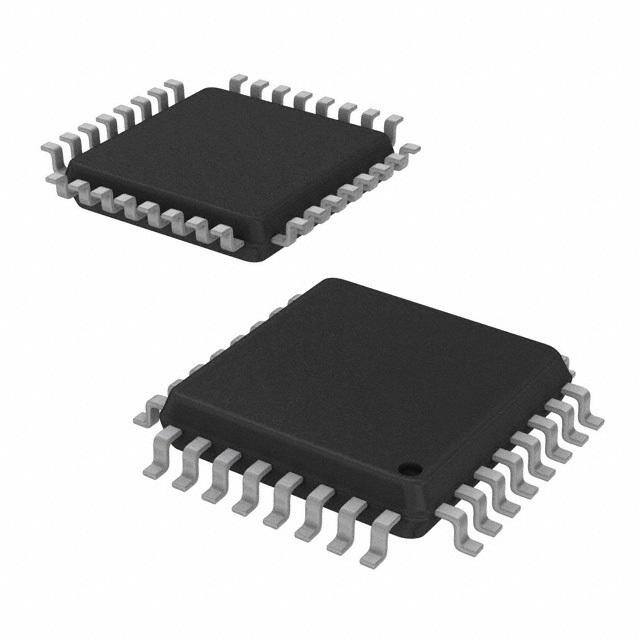
| 供应商器件封装 | 32-LQFP(7x7) |
| 其它名称 | MC100EP196FAGOS |
| 功能 | 可编程 |
| 包装 | 托盘 |
| 可用总延迟 | 2.36ns ~ 12.258ns |
| 商标 | ON Semiconductor |
| 安装类型 | 表面贴装 |
| 安装风格 | SMD/SMT |
| 封装 | Tray |
| 封装/外壳 | 32-LQFP |
| 封装/箱体 | LQFP-32 |
| 工作温度 | -40°C ~ 85°C |
| 工厂包装数量 | 250 |
| 延迟到第一抽头 | 2.36ns |
| 抽头/步数 | 1024 |
| 抽头增量 | 10ps |
| 最大工作温度 | + 85 C |
| 最小工作温度 | - 40 C |
| 标准包装 | 250 |
| 独立延迟数 | 1 |
| 电压-电源 | 3 V ~ 3.6 V |
| 电源电压-最大 | +/- 3.6 V |
| 电源电压-最小 | +/- 3 V |
| 系列 | MC100EP196 |
| 零件号别名 | MC100EP196BMNG |


PDF Datasheet 数据手册内容提取
MC100EP196 3.3V ECL Programmable Delay Chip with FTUNE The MC100EP196 is a programmable delay chip (PDC) designed primarily for clock deskewing and timing adjustment. It provides variable delay of a differential NECL/PECL input transition. It has similar architecture to the EP195 with the added feature of further tuneability in http://onsemi.com delay using the FTUNE pin. The FTUNE input takes an analog voltage from V to V to fine tune the output delay from 0 to 60 ps. CC EE MARKING The delay section consists of a programmable matrix of gates and DIAGRAM* multiplexers as shown in the logic diagram, Figure 2. The delay increment of the EP196 has a digitally selectable resolution of about 10 ps and a net range of up to 10.2 ns. The required delay is selected by the 10 data select inputs D[9:0] values and controlled by the LEN (pin 10). A LOW level on MC100 LEN allows a transparent LOAD mode of real time delay values by EP196 D[9:0]. A LOW to HIGH transition on LEN will LOCK and HOLD LQFP−32 AWLYYWWG current values present against any subsequent changes in D[10:0]. The FA SUFFIX 32 approximate delay values for varying tap numbers correlating to D0 (LSB) CASE 873A through D9 (MSB) are shown in Table 5. 1 Because the EP196 is designed using a chain of multiplexers, it has a fixed minimum delay of 2.4 ns. An additional pin, D10, is provided for A = Assembly Location controlling Pins 14 and 15, CASCADE and CASCADE, also latched WL = Wafer Lot by LEN, in cascading multiple PDCs for increased programmable YY = Year WW = Work Week range. The cascade logic allows full control of multiple PDCs. G = Pb−Free Package Switching devices from all “1” states on D[0:9] with SETMAX LOW to all “0” states on D[0:9] with SETMAX HIGH will increase the *For additional marking information, refer to delay equivalent to “D0”, the minimum increment. Application Note AND8002/D. Select input pins, D[10:0], may be threshold controlled by combinations of interconnects between V (pin 7) and V (pin 8) EF CF for LVCMOS, ECL, or LVTTL level signals. LVTTL and LVCMOS ORDERING INFORMATION operation is available in PECL mode only. For LVCMOS input levels, See detailed ordering and shipping information in the package leave VCF and VEF open. For ECL operation, short VCF and VEF dimensions section on page 17 of this data sheet. (pins 7 and 8). For LVTTL level operation, connect a 1.5 V supply reference to V and leave open V pin. The 1.5 V reference voltage CF EF to V pin can be accomplished by placing a 2.2 k(cid:2) resistor between CF V and V for 3.3 V power supply. *For additional information on our Pb−Free strategy CF EE and soldering details, please download the The V pin, an internally generated voltage supply, is available to BB ON Semiconductor Soldering and Mounting this device only. For single−ended input conditions, the unused Techniques Reference Manual, SOLDERRM/D. differential input is connected to V as a switching reference voltage. BB V may also rebias AC coupled inputs. When used, decouple V BB BB and V via a 0.01 (cid:3)F capacitor and limit current sourcing or sinking CC to 0.5 mA. When not used, V should be left open. BB The 100 Series contains temperature compensation. • • Maximum Frequency > 1.2 GHz Typical Open Input Default State • • Programmable Range: 0 ns to 10 ns Safety Clamp on Inputs • • Delay Range: 2.4 ns to 12.4 ns A Logic High on the EN Pin Will Force Q to Logic • 10 ps Increments Low • PECL Mode Operating Range: • D[10:0] Can Accept Either ECL, LVCMOS, or LVTTL VCC = 3.0 V to 3.6 V with VEE = 0 V Inputs • NECL Mode Operating Range: • VBB Output Reference Voltage • VCC = 0 V with VEE = −3.0 V to −3.6 V These are Pb−Free Devices* © Semiconductor Components Industries, LLC,2014 1 Publication Order Number: June, 2014 − Rev. 16 MC100EP196/D
MC100EP196 VEE D0 VCC Q Q VCC VCCFTUNE 24 23 22 21 20 19 18 17 D1 25 16 EN D2 26 15 CASCADE D3 27 14 CASCADE VEE 28 13 VCC MC100EP196 D4 29 12 SETMAX D5 30 11 SETMIN 31 10 D6 LEN D7 32 9 VEE 1 2 3 4 5 6 7 8 D8 D9 D10 IN IN VBB VEF VCF Figure 1. 32−Lead LQFP Pinout (Top View) http://onsemi.com 2
MC100EP196 Table 1. PIN DESCRIPTION Pin Name I/O Default State Description 23, 25, 26, 27, D[0:9] LVCMOS, LVTTL, LOW Single−ended Parallel Data Inputs [0:9]. Internal 75 k(cid:2) to VEE. 29, 30, 31, 32, ECL Input (Note 1) 1, 2 3 D[10] LVCMOS, LVTTL, LOW Single−ended CASCADE/CASCADE Control Input. Internal 75 k(cid:2) ECL Input to VEE. (Note 1) 4 IN ECL Input LOW Noninverted Differential Input. Internal 75 k(cid:2) to VEE. 5 IN ECL Input HIGH Inverted Differential Input. Internal 75 k(cid:2) to VEE. 6 VBB − − ECL Reference Voltage Output 7 VEF − − Reference Voltage for ECL Mode Connection 8 VCF − − LVCMOS, ECL, OR LVTTL Input Mode Select 9, 28 VEE − − Negative Supply Voltage. All VEE Pins must be Externally Connec- ted to Power Supply to Guarantee Proper Operation. (Note 2) 13, 18, 19, 22 VCC − − Positive Supply Voltage. All VCC Pins must be externally Connec- ted to Power Supply to Guarantee Proper Operation. (Note 2) 10 LEN ECL Input LOW Single−ended D pins LOAD / HOLD input. Internal 75 k(cid:2) to VEE. 11 SETMIN ECL Input LOW Single−ended Minimum Delay Set Logic Input. Internal 75 k(cid:2) to VEE. (Note 1) 12 SETMAX ECL Input LOW Single−ended Maximum Delay Set Logic Input. Internal 75 k(cid:2) to VEE. (Note 1) 14 CASCADE ECL Output − Inverted Differential Cascade Output for D[10] Input. Typically Ter- minated with 50 (cid:2) to VTT = VCC − 2 V. 15 CASCADE ECL Output − Noninverted Differential Cascade Output for D[10] Input. Typically Terminated with 50 (cid:2) to VTT = VCC − 2 V. 16 EN ECL Input LOW Single−ended Output Enable Pin. Internal 75 k(cid:2) to VEE. 17 FTUNE Analog Input − Fine Tuning Input. 21 Q ECL Output − Noninverted Differential Output. Typically Terminated with 50 (cid:2) to VTT = VCC − 2 V. 20 Q ECL Output − Inverted Differential Output. Typically Terminated with 50 (cid:2) to VTT = VCC − 2 V. 1. SETMIN will override SETMAX if both are high. SETMAX and SETMIN will override all D[0:10] inputs. 2. All VCC and VEE pins must be externally connected to Power Supply to guarantee proper operation. http://onsemi.com 3
MC100EP196 Table 2. CONTROL PIN Pin State Function EN LOW (Note 3) Input Signal is Propagated to the Output HIGH Output Holds Logic Low State LEN LOW (Note 3) Transparent or LOAD mode for real time delay values present on D[0:10]. HIGH LOCK and HOLD mode for delay values on D[0:10]; further changes on D[0:10] are not recognized and do not affect delay. SETMIN LOW (Note 3) Output Delay set by D[0:10] HIGH Set Minimum Output Delay SETMAX LOW (Note 3) Output Delay set by D[0:10] HIGH Set Maximum Output Delay D10 LOW CASCADE Output LOW, CASCADE Output HIGH HIGH CASCADE Output LOW, CASCADE Output High 3. Internal pulldown resistor will provide a logic LOW if pin is left unconnected. Table 3. CONTROL D[0:10] INTERFACE Pin State Function VCF VEF Pin (Note 4) ECL Mode V No Connect LVCMOS Mode CF VCF 1.5 V (cid:2) 100 mV LVTTL Mode (Note 5) 4. Short VCF (pin 8) and VEF (pin 7). 5. When Operating in LVTTL Mode, the reference voltage can be provided by connecting an external resistor, RCF (suggested resistor value is 2.2 k(cid:2) (cid:2)5%), between VCF and VEE pins. Table 4. DATA INPUT ALLOWED OPERATING VOLTAGE MODE TABLE CONTROL DATA SELECT INPUTS PINS (D [0:10]) POWER SUPPLY LVCMOS LVTTL LVPECL LVNECL PECL Mode Operating Range YES YES YES N/A NECL Mode Operating Range N/A N/A N/A YES http://onsemi.com 4
MC100EP196 Q Q 0 1 1D* G 00 11 11GD*GD* D0 E T 0 1 D1 GA 2D* ER G P Y A L 0 1 D2 DE ns) 4GD* Y 10 ps OX. 2.4 0 1 D3 ATEL PPR M A 8GD* OXI LAY R E P D 0 161GD* T LATCH D4 ELAY) AP MINIMUM 0 1 10 BI D5 ATE D XED G FI 2D* = ( ( 3G D G * 6 0 1 D 4D* 6G E E 7 D D 0 1 D A A C C S S 128GD* CA CA 8 0 1 D 56D* 2G h c 0 Lat D1 9 0 1 D 12D* 5G N N X LE ET MI ET MA S S B F F E UNE IN IN EN VB VC VE VE T F Figure 2. Logic Diagram http://onsemi.com 5
MC100EP196 Table 5. THEORETICAL DELTA DELAY VALUES D(9:0) Value SETMIN SETMAX Programmable Delay* XXXXXXXXXX H L 0 ps 0000000000 L L 0 ps 0000000001 L L 10 ps 0000000010 L L 20 ps 0000000011 L L 30 ps 0000000100 L L 40 ps 0000000101 L L 50 ps 0000000110 L L 60 ps 0000000111 L L 70 ps 0000001000 L L 80 ps 0000010000 L L 160 ps 0000100000 L L 320 ps 0001000000 L L 640 ps 0010000000 L L 1280 ps 0100000000 L L 2560 ps 1000000000 L L 5120 ps 1111111111 L L 10230 ps XXXXXXXXXX L H 10240 ps *Fixed minimum delay not included. Table 6. TYPICAL FTUNE DELAY PIN Input Range Output Range VCC−VEE (V) 0 − 60 (ps) http://onsemi.com 6
MC100EP196 15000 14000 13000 85 °C 12000 11000 25 °C 10000 −40 °C s) 9000 p Y ( 8000 A L E D 7000 6000 5000 4000 3000 2000 1000 0 0 100 200 300 400 500 600 700 800 900 1000 Decimal Value of Select Inputs (D[9:0]) Figure 3. Measured Delay vs. Select Inputs Table 7. ATTRIBUTES Characteristics Value Internal Input Pulldown Resistor 75 k(cid:2) Internal Input Pullup Resistor N/A ESD Protection Human Body Model > 2 kV Machine Model > 100 V Charged Device Model > 2 kV Moisture Sensitivity, Indefinite Time Out of Drypack (Note 1) Pb−Free Pkg LQFP−32 Level 2 Flammability RatingOxygen Index: 28 to 34 UL 94 V−0 @ 0.125 in Transistor Count 1237 Devices Meets or exceeds JEDEC Spec EIA/JESD78 IC Latchup Test 1. For additional information, see Application Note AND8003/D. http://onsemi.com 7
MC100EP196 Table 8. MAXIMUM RATINGS Symbol Parameter Condition 1 Condition 2 Rating Units VCC PECL Mode Power Supply VEE = 0 V 6 V VEE NECL Mode Power Supply VCC = 0 V −6 V VI PECL Mode Input Voltage VEE = 0 V VI ≤ VCC 6 V NECL Mode Input Voltage VCC = 0 V VI ≥ VEE −6 V Iout Output Current Continuous 50 mA Surge 100 mA IBB VBB Sink/Source ± 0.5 mA TA Operating Temperature Range −40 to +85 °C Tstg Storage Temperature Range −65 to +150 °C (cid:4) Thermal Resistance (Junction−to−Ambient) 0 lfpm LQFP−32 80 °C/W JA 500 lfpm LQFP−32 55 °C/W (cid:4) Thermal Resistance (Junction−to−Case) Standard Board LQFP−32 12 to 17 °C/W JC Tsol Wave Solder Pb−Free 265 °C Stresses exceeding those listed in the Maximum Ratings table may damage the device. If any of these limits are exceeded, device functionality should not be assumed, damage may occur and reliability may be affected. http://onsemi.com 8
MC100EP196 Table 9. DC CHARACTERISTICS, PECL VCC = 3.3 V, VEE = 0 V (Note 2) −40°C 25°C 85°C Symbol Characteristic Min Typ Max Min Typ Max Min Typ Max Unit IEE Power Supply Current 100 125 160 110 130 170 110 135 175 mA VOH Output HIGH Voltage (Note 3) 2155 2300 2405 2155 2300 2405 2155 2300 2405 mV VOL Output LOW Voltage (Note 3) 1305 1520 1605 1305 1500 1605 1305 1485 1605 mV VIH Input HIGH Voltage (Single−Ended) mV LVPECL 2075 2420 2075 2420 2075 2420 LVCMOS 2000 3300 2000 3300 2000 3300 LVTTL 2000 3300 2000 3300 2000 3300 VIL Input LOW Voltage (Single−Ended) mV LVPECL 1305 1675 1305 1675 1305 1675 LVCMOS 0 800 0 800 0 800 LVTTL 0 800 0 800 0 800 VBB Output Voltage Reference 1775 1875 1975 1775 1875 1975 1775 1875 1975 mV VCF LVTTL Mode Input Detect Voltage 1.4 1.5 1.6 1.4 1.5 1.6 1.4 1.5 1.6 V @ IVCF = 700 (cid:3)A VEF Reference Voltage for 1900 1960 2050 1875 1953 2050 1850 1945 2050 mV ECL Mode Connection VIHCMR Input HIGH Voltage Common Mode 2.0 3.3 2.0 3.3 2.0 3.3 V Range (Differential Configuration) (Note 4) IIH Input HIGH Current (PECL) (cid:3)A IN, IN, EN, LEN, SETMIN, SETMAX 150 150 150 IIHH FTUNE Input High Current @ VCC 50 87 150 50 84 150 50 82 150 (cid:3)A IIL Input LOW Current (PECL) (cid:3)A IN, IN, EN, LEN, SETMIN, SETMAX 0.5 0.5 0.5 IILL FTUNE Input LOW Current @VEE −10 0 10 −10 0 10 −10 0 10 (cid:3)A NOTE:Device will meet the specifications after thermal equilibrium has been established when mounted in a test socket or printed circuit board with maintained transverse airflow greater than 500 lfpm. Electrical parameters are guaranteed only over the declared operating temperature range. Functional operation of the device exceeding these conditions is not implied. Device specification limit values are applied individually under normal operating conditions and not valid simultaneously. 2. Input and output parameters vary 1:1 with VCC. VEE can vary +0.3 V to −0.3 V. 3. All loading with 50 (cid:2) to VCC − 2.0 V. 4. VIHCMR min varies 1:1 with VEE, VIHCMR max varies 1:1 with VCC. The VIHCMR range is referenced to the most positive side of the differential input signal. http://onsemi.com 9
MC100EP196 Table 10. DC CHARACTERISTICS, NECL VCC = 0 V, VEE = −3.3 V (Note 5) −40°C 25°C 85°C Symbol Characteristic Min Typ Max Min Typ Max Min Typ Max Unit IEE Power Supply Current 100 125 160 110 130 170 110 135 175 mA VOH Output HIGH Voltage (Note 6) −1145 −1000 −895 −1145 −1000 −895 −1145 −1000 −895 mV VOL Output LOW Voltage (Note 6) −1995 −1780 −1695 −1995 −1800 −1695 −1995 −1815 −1695 mV VIH Input HIGH Voltage (Single−Ended) mV LVNECL −1225 −880 −1225 −880 −1225 −880 VIL Input LOW Voltage (Single−Ended) mV LVNECL −1995 −1625 −1995 −1625 −1995 −1625 VBB Output Voltage Reference −1525 −1425 −1325 −1525 −1425 −1325 −1525 −1425 −1325 mV VEF Reference Voltage for ECL Mode −1400 −1340 −1250 −1425 −1347 −1250 −1450 −1355 −1250 mV Connection VIHCMR Input HIGH Voltage Common Mode VEE+2.0 0 VEE+2.0 0 VEE+2.0 0 V Range (Differential Configuration) (Note 7) IIH Input HIGH Current (cid:3)A IN, IN, EN, LEN, SETMIN, SETMAX 150 150 150 IIHH FTUNE Input High Current @ VCC 50 87 150 50 84 150 50 82 150 (cid:3)A IIL Input LOW Current (cid:3)A IN, IN, EN, LEN, SETMIN, SETMAX 0.5 0.5 0.5 IILL FTUNE Input LOW Current @ VEE −10 0 10 −10 0 10 −10 0 10 (cid:3)A NOTE:Device will meet the specifications after thermal equilibrium has been established when mounted in a test socket or printed circuit board with maintained transverse airflow greater than 500 lfpm. Electrical parameters are guaranteed only over the declared operating temperature range. Functional operation of the device exceeding these conditions is not implied. Device specification limit values are applied individually under normal operating conditions and not valid simultaneously. 5. Input and output parameters vary 1:1 with VCC. VEE can vary +0.3 V to −0.3 V. 6. All loading with 50 (cid:2) to VCC − 2.0 V. 7. VIHCMR min varies 1:1 with VEE, VIHCMR max varies 1:1 with VCC. The VIHCMR range is referenced to the most positive side of the differential input signal. http://onsemi.com 10
MC100EP196 Table 11. AC CHARACTERISTICS VCC = 0 V; VEE = −3.0 V to −3.6 V or VCC = 3.0 V to 3.6 V; VEE = 0 V (Note 8) −40°C 25°C 85°C Symbol Characteristic Min Typ Max Min Typ Max Min Typ Max Unit fmax Maximum Frequency 1.2 1.2 1.2 GHz tPLH Propagation Delay ps tPHL IN to Q; D(0−9) = 0 1810 2210 2610 1960 2360 2760 2180 2580 2980 IN to Q; D(0−9) = 1023 9500 11496 13500 10000 12258 14000 10955 13454 15955 EN to Q; D(0−9) = 0 1780 2277 2780 1930 2430 2930 2150 2650 3150 D10 to CASCADE 350 450 550 380 477 580 420 520 620 tRANGE Programmable Range ps {D(0−9) = HI} − {D(0−9) = LO} 8600 9285 10000 9200 9897 10700 9900 10875 12000 (cid:5)t Step Delay (Note 9) ps D0 High 7 11 13 D1 High 23 30 32 D2 High 39 48 53 D3 High 58 67 73 D4 High 90 137 185 100 149 200 90 154 225 D5 High 245 293 335 260 313 370 270 337 410 D6 High 530 590 650 560 629 710 600 681 770 D7 High 1060 1158 1265 1130 1237 1355 1200 1353 1520 D8 High 2160 2317 2490 2290 2472 2680 2450 2712 3015 D9 High 4335 4647 5010 4590 4955 5385 4935 5440 6015 Mono Monotonicity (Note 10) ps tSKEW Duty Cycle Skew (Note 11) ps |tPHL−tPLH| 20 22 27 ts Setup Time ps D to LEN 150 −10 150 −70 150 −70 D to IN (Note 12) 100 −130 100 −150 100 −165 EN to IN (Note 13) 150 −105 150 −120 150 −140 th Hold Time ps LEN to D 225 170 200 70 200 60 IN to EN (Note 14) 450 275 450 305 450 325 tR Release Time ps EN to IN (Note 15) 150 −105 150 −120 150 −140 SET MAX to LEN 400 70 400 110 400 160 SET MIN to LEN 300 165 350 180 350 205 tjit Random Clock Jitter 3 3 3 ps @ 1.2 GHz, SETMAX Delay VPP Input Voltage Swing 150 800 1200 150 800 1200 150 800 1200 mV (Differential Configuration) tr Output Rise/Fall Time ps tf 20−80% (Q) 85 110 130 95 120 145 110 135 160 20−80% (CASCADE) 100 150 200 110 160 210 125 175 225 NOTE:Device will meet the specifications after thermal equilibrium has been established when mounted in a test socket or printed circuit board with maintained transverse airflow greater than 500 lfpm. Electrical parameters are guaranteed only over the declared operating temperature range. Functional operation of the device exceeding these conditions is not implied. Device specification limit values are applied individually under normal operating conditions and not valid simultaneously. 8. Measured using a 750 mV source, 50% duty cycle clock source. All loading with 50 (cid:2) to VCC − 2.0 V. 9. Specification limits represent the amount of delay added with the assertion of each individual delay control pin. The various combinations of asserted delay control inputs will typically realize D0 resolution steps across the specified programmable range. 10.The monotonicity indicates the increased delay value for each binary count increment on the control inputs D(0−9). 11.Duty cycle skew guaranteed only for differential operation measured from the cross point of the input to the cross point of the output. 12.This setup time defines the amount of time prior to the input signal the delay tap of the device must be set. 13.This setup time is the minimum time that EN must be asserted prior to the next transition of IN/IN to prevent an output response greater than VCC − 1425 mV to that IN/IN transition. 14.This hold time is the minimum time that EN must remain asserted after a negative going IN or positive going IN to prevent an output response greater than VCC − 1425 mV to that IN/IN transition. 15.This release time is the minimum time that EN must be deasserted prior to the next IN/IN transition to ensure an output response that meets the specified IN to Q propagation delay and transition times. http://onsemi.com 11
MC100EP196 IN VINPP = VIH(D) − VIL(D) IN Q VOUTPP = VOH(Q) − VOL(Q) Q tPHL tPLH Figure 4. AC Reference Measurement Using the FTUNE Analog Input FTUNE pin will be capable even under worst case The analog FTUNE pin on the EP196 device is intended conditions of covering a digital resolution. Typically, the to add more delay in a tunable gate to enhance the 10 ps analog input will be driven by an external DAC to provide a digital control with very fine analog output steps. The final resolution capabilities of the fully digital EP196. The level resolution of the device will be dependent on the width of the of resolution obtained is dependent on the voltage applied to DAC chosen. the FTUNE pin. To determine the voltage range necessary for the FTUNE To provide this further level of resolution, the FTUNE pin input, Figure 5 should be used. There are numerous voltage must be capable of adjusting the additional delay finer than ranges which can be used to cover a given delay range; users the 10 ps digital resolution (See Logic Diagram). This requirement is easily achieved because a 60 ps additional are given the flexibility to determine which one best fits their delay can be obtained over the entire FTUNE voltage range designs. (See Figure 5). This extra analog range ensures that the 90 80 VCC = 0 V VEE = −3.3 V −40°C 70 25°C 60 s) 50 p AY ( 40 L E D 30 20 85°C 10 0 −10 −3.3 −2.97 −2.64 −2.31 −1.98 −1.65 −1.32 −0.99 −0.66 −0.33 0 VEE VCC FTUNE VOLTAGE (V) Figure 5. Typical EP196 Delay versus FTUNE Voltage http://onsemi.com 12
MC100EP196 Cascading Multiple EP196s expanded for larger EP196 chains. The D10 input of the To increase the programmable range of the EP196, EP196 is the cascade control pin and when assert internal cascade circuitry has been included. This circuitry HIGH switches output pin CASCADE to HIGH and pin CASCADE to LOW. With the interconnect scheme of allows for the cascading of multiple EP196s without the Figure 6 when D10 is asserted, it signals the need for a larger need for any external gating. Furthermore, this capability programmable range than is achievable with a single device. requires only one more address line per added E196. The A11 address can be added to generate a cascade output Obviously, cascading multiple programmable delay chips for the next EP196. For a 2−device configuration, A11 is not will result in a larger programmable range; however, this required. increase is at the expense of a longer minimum delay. Figure 6 illustrates the interconnect scheme for cascading two EP196s. As can be seen, this scheme can easily be Need if Chip #3 is used ADDRESS BUS A11 A10 A9 A8 A7A6 A5A4 A3 A2 A1 A0 D7 D6 D5 D4 VEE D3 D2 D1 D7 D6 D5 D4 VEE D3 D2 D1 D8 VEE D8 VEE D9 D0 D9 D0 D10 VCC D10 VCC EP196 EP196 IN Q IN Q INPUT OUTPUT IN Q IN Q CHIP #2 CHIP #1 VBB VCC VBB VCC VEF VCC VEF VCC E E E E VCF N AX AD AD FTUNE VCF N AX AD AD FTUNE MI M C C MI M C C EE EN ET ET CC AS AS N EE EN ET ET CC AS AS N V L S S V C C E V L S S V C C E DAC Figure 6. Cascading Interconnect Architecture http://onsemi.com 13
MC100EP196 An expansion of the latch section of the block diagram is chip #2 will be deasserted and the SETMAX pin asserted, pictured in Figure 7. Use of this diagram will simplify the resulting in the device delay to be the maximum delay. explanation of how the SETMIN and SETMAX circuitry Table 12 shows the delay time of two EP196 chips in works in cascade. When D10 of chip #1 in Figure 5 is LOW, cascade. this device’s cascade output will also be LOW while the To expand this cascading scheme to more devices, one CASCADE output will be HIGH. In this condition, the simply needs to connect the D10 pin from the next chip to SETMIN pin of chip #2 will be asserted HIGH and thus all the address bus and CASCADE outputs to the next chip in of the latches of chip #2 will be reset and the device will be the same manner as pictured in Figure 6. The only addition set at its minimum delay. to the logic is the increase of one line to the address bus for Chip #1, on the other hand, will have both SETMIN and cascade control of the second programmable delay chip. SETMAX deasserted so that its delay will be controlled Furthermore, to fully utilize EP196, the FTUNE pin can entirely by the address bus A0−A9. If the delay needed is be used for additional delay and for finer resolution than greater than can be achieved with 1023 gate delays 10 ps. As shown in Figure 5, an analog voltage input from (1111111111 on the A0−A9 address bus), D10 will be DAC can adjust the FTUNE pin with an extra 60 ps of delay asserted to signal the need to cascade the delay to the next for each chip. EP196 device. When D10 is asserted, the SETMIN pin of TO SELECT MULTIPLEXERS BIT 0 BIT 1 BIT 2 BIT 3 BIT 4 BIT 5 BIT 6 BIT 7 BIT 8 BIT 9 D0 Q0 D1 Q1 D2 Q2 D3 Q3 D4 Q4 D5 Q5 D6 Q6 D7 Q7 D8 Q8 D9 Q9 LEN LEN LEN LEN LEN LEN LEN LEN LEN LEN Set Reset Set Reset Set Reset Set Reset Set Reset Set Reset Set Reset Set Reset Set Reset Set Reset SET MIN SET MAX Figure 7. Expansion of the Latch Section of the EP196 Block Diagram http://onsemi.com 14
MC100EP196 Table 12. CASCADED DELAY VALUE OF TWO EP196S VARIABLE INPUT TO CHIP #1 AND SETMIN FOR CHIP #2 INPUT FOR CHIP #1 Total D10 D9 D8 D7 D6 D5 D4 D3 D2 D1 D0 Delay Value Delay Value 0 0 0 0 0 0 0 0 0 0 0 0 ps 4400 ps 0 0 0 0 0 0 0 0 0 0 1 10 ps 4410 ps 0 0 0 0 0 0 0 0 0 1 0 20 ps 4420 ps 0 0 0 0 0 0 0 0 0 1 1 30 ps 4430 ps 0 0 0 0 0 0 0 0 1 0 0 40 ps 4440 ps 0 0 0 0 0 0 0 0 1 0 1 50 ps 4450 ps 0 0 0 0 0 0 0 0 1 1 0 60 ps 4460 ps 0 0 0 0 0 0 0 0 1 1 1 70 ps 4470 ps 0 0 0 0 0 0 0 1 0 0 0 80 ps 4480 ps 0 0 0 0 0 0 1 0 0 0 0 160 ps 4560 ps 0 0 0 0 0 1 0 0 0 0 0 320 ps 4720 ps 0 0 0 0 1 0 0 0 0 0 0 640 ps 5040 ps 0 0 0 1 0 0 0 0 0 0 0 1280 ps 5680 ps 0 0 1 0 0 0 0 0 0 0 0 2560 ps 6960 ps 0 1 0 0 0 0 0 0 0 0 0 5120 ps 9520 ps 0 1 1 1 1 1 1 1 1 1 1 10230 ps 14630 ps VARIABLE INPUT TO CHIP #1 AND SETMAX FOR CHIP #2 INPUT FOR CHIP #1 Total D10 D9 D8 D7 D6 D5 D4 D3 D2 D1 D0 Delay Value Delay Value 1 0 0 0 0 0 0 0 0 0 0 10240 ps 14640 ps 1 0 0 0 0 0 0 0 0 0 1 10250 ps 14650 ps 1 0 0 0 0 0 0 0 0 1 0 10260 ps 14660 ps 1 0 0 0 0 0 0 0 0 1 1 10270 ps 14670 ps 1 0 0 0 0 0 0 0 1 0 0 10280 ps 14680 ps 1 0 0 0 0 0 0 0 1 0 1 10290 ps 14690 ps 1 0 0 0 0 0 0 0 1 1 0 10300 ps 14700 ps 1 0 0 0 0 0 0 0 1 1 1 10310 ps 14710 ps 1 0 0 0 0 0 0 1 0 0 0 10320 ps 14720 ps 1 0 0 0 0 0 1 0 0 0 0 10400 ps 14800 ps 1 0 0 0 0 1 0 0 0 0 0 10560 ps 14960 ps 1 0 0 0 1 0 0 0 0 0 0 10880 ps 15280 ps 1 0 0 1 0 0 0 0 0 0 0 11520 ps 15920 ps 1 0 1 0 0 0 0 0 0 0 0 12800 ps 17200 ps 1 1 0 0 0 0 0 0 0 0 0 15360 ps 19760 ps 1 1 1 1 1 1 1 1 1 1 1 20470 ps 24870 ps http://onsemi.com 15
MC100EP196 Multi−Channel Deskewing Figure 8. One signal channel can be used as reference and the The most practical application for EP196 is in multiple other EP196s can be used to adjust the delay to eliminate the channel delay matching. Slight differences in impedance timing skews. Nearly any high−speed system can be fine tuned (as small as 10 ps) to reduce the skew to extremely and cable length can create large timing skews within a tight tolerances using the available FTUNE pin. high−speed system. To deskew multiple signal channels, each channel can be sent through each EP196 as shown in EP196 IN Q IN Q #1 EP196 IN Q IN Q #2 EP196 IN Q IN Q #N Digital Data Control DAC Logic Figure 8. Multiple Channel Deskewing Diagram http://onsemi.com 16
MC100EP196 Q Zo = 50 (cid:2) D Driver Receiver Device Device Q Zo = 50 (cid:2) D 50 (cid:2) 50 (cid:2) VTT VTT = VCC − 2.0 V Figure 9. Typical Termination for Output Driver and Device Evaluation (See Application Note AND8020/D − Termination of ECL Logic Devices.) ORDERING INFORMATION Device Package Shipping† MC100EP196FAG LQFP−32 250 Units / Tray (Pb−Free) MC100EP196FAR2G LQFP−32 2000 / Tape & Reel (Pb−Free) †For information on tape and reel specifications, including part orientation and tape sizes, please refer to our Tape and Reel Packaging Specifications Brochure, BRD8011/D. Resource Reference of Application Notes AN1405/D − ECL Clock Distribution Techniques AN1406/D − Designing with PECL (ECL at +5.0 V) AN1503/D − ECLinPS(cid:2) I/O SPiCE Modeling Kit AN1504/D − Metastability and the ECLinPS Family AN1568/D − Interfacing Between LVDS and ECL AN1672/D − The ECL Translator Guide AND8001/D − Odd Number Counters Design AND8002/D − Marking and Date Codes AND8020/D − Termination of ECL Logic Devices AND8066/D − Interfacing with ECLinPS AND8090/D − AC Characteristics of ECL Devices http://onsemi.com 17
MC100EP196 PACKAGE DIMENSIONS 32 LEAD LQFP CASE 873A−02 ISSUE C − Z − −, U A1 A 4X 0.20 (0.008) AB T-U Z T−, − 32 25 − 1 AE −T− −U− P B V AE B1 DETAIL Y V1 DETAIL Y BASE Z 8 17 METAL U - ÉÉN T C 9 A −Z− 4X ÉÉ M 9 S1 0.20 (0.008) AC T-U Z ÉF É D 8) 0 S ÉÉ 0 (0.0 8XM(cid:3) J 0.2 R DETAIL AD G SECTION AE−AE −AB− E C SEATING −AC− PLANE 0.10 (0.004) AC H W K Q(cid:3) 0) DETAIL AD X GE PLANE 50 (0.01 GAU 0.2 NOTES: MILLIMETERS INCHES 1. DIMENSIONING AND TOLERANCING PER ANSI Y14.5M, 1982. DIM MIN MAX MIN MAX 2. CONTROLLING DIMENSION: A 7.000 BSC 0.276 BSC MILLIMETER. A1 3.500 BSC 0.138 BSC 3. DATUM PLANE −AB− IS LOCATED AT B 7.000 BSC 0.276 BSC BOTTOM OF LEAD AND IS COINCIDENT B1 3.500 BSC 0.138 BSC WITH THE LEAD WHERE THE LEAD C 1.400 1.600 0.055 0.063 EXITS THE PLASTIC BODY AT THE D 0.300 0.450 0.012 0.018 BOTTOM OF THE PARTING LINE. E 1.350 1.450 0.053 0.057 4. DATUMS −T−, −U−, AND −Z− TO BE F 0.300 0.400 0.012 0.016 DETERMINED AT DATUM PLANE −AB−. G 0.800 BSC 0.031 BSC 5. DIMENSIONS S AND V TO BE H 0.050 0.150 0.002 0.006 DETERMINED AT SEATING PLANE −AC−. J 0.090 0.200 0.004 0.008 6. DIMENSIONS A AND B DO NOT INCLUDE K 0.450 0.750 0.018 0.030 MPROOLTDR PURSOIOTNR UISS I0O.2N5. 0 A(0L.L0O10W) APBELRE SIDE. M 12(cid:3) REF 12(cid:3) REF DIMENSIONS A AND B DO INCLUDE N 0.090 0.160 0.004 0.006 MOLD MISMATCH AND ARE P 0.400 BSC 0.016 BSC DETERMINED AT DATUM PLANE −AB−. Q 1(cid:3) 5 (cid:3) 1(cid:3) 5 (cid:3) 7. DIMENSION D DOES NOT INCLUDE R 0.150 0.250 0.006 0.010 DAMBAR PROTRUSION. DAMBAR S 9.000 BSC 0.354 BSC PROTRUSION SHALL NOT CAUSE THE S1 4.500 BSC 0.177 BSC D DIMENSION TO EXCEED 0.520 (0.020). V 9.000 BSC 0.354 BSC 8. MINIMUM SOLDER PLATE THICKNESS V1 4.500 BSC 0.177 BSC SHALL BE 0.0076 (0.0003). W 0.200 REF 0.008 REF 9. EXACT SHAPE OF EACH CORNER MAY X 1.000 REF 0.039 REF VARY FROM DEPICTION. http://onsemi.com 18
MC100EP196 ECLinPS is a trademark of Semiconductor Components Industries, LLC. ON Semiconductor and are registered trademarks of Semiconductor Components Industries, LLC (SCILLC). SCILLC owns the rights to a number of patents, trademarks, copyrights, trade secrets, and other intellectual property. A listing of SCILLC’s product/patent coverage may be accessed at www.onsemi.com/site/pdf/Patent−Marking.pdf. SCILLC reserves the right to make changes without further notice to any products herein. SCILLC makes no warranty, representation or guarantee regarding the suitability of its products for any particular purpose, nor does SCILLC assume any liability arising out of the application or use of any product or circuit, and specifically disclaims any and all liability, including without limitation special, consequential or incidental damages. “Typical” parameters which may be provided in SCILLC data sheets and/or specifications can and do vary in different applications and actual performance may vary over time. All operating parameters, including “Typicals” must be validated for each customer application by customer’s technical experts. SCILLC does not convey any license under its patent rights nor the rights of others. SCILLC products are not designed, intended, or authorized for use as components in systems intended for surgical implant into the body, or other applications intended to support or sustain life, or for any other application in which the failure of the SCILLC product could create a situation where personal injury or death may occur. Should Buyer purchase or use SCILLC products for any such unintended or unauthorized application, Buyer shall indemnify and hold SCILLC and its officers, employees, subsidiaries, affiliates, and distributors harmless against all claims, costs, damages, and expenses, and reasonable attorney fees arising out of, directly or indirectly, any claim of personal injury or death associated with such unintended or unauthorized use, even if such claim alleges that SCILLC was negligent regarding the design or manufacture of the part. SCILLC is an Equal Opportunity/Affirmative Action Employer. This literature is subject to all applicable copyright laws and is not for resale in any manner. PUBLICATION ORDERING INFORMATION LITERATURE FULFILLMENT: N. American Technical Support: 800−282−9855 Toll Free ON Semiconductor Website: www.onsemi.com Literature Distribution Center for ON Semiconductor USA/Canada P.O. Box 5163, Denver, Colorado 80217 USA Europe, Middle East and Africa Technical Support: Order Literature: http://www.onsemi.com/orderlit Phone: 303−675−2175 or 800−344−3860 Toll Free USA/Canada Phone: 421 33 790 2910 Fax: 303−675−2176 or 800−344−3867 Toll Free USA/Canada Japan Customer Focus Center For additional information, please contact your local Email: orderlit@onsemi.com Phone: 81−3−5817−1050 Sales Representative http://onsemi.com MC100EP196/D 19