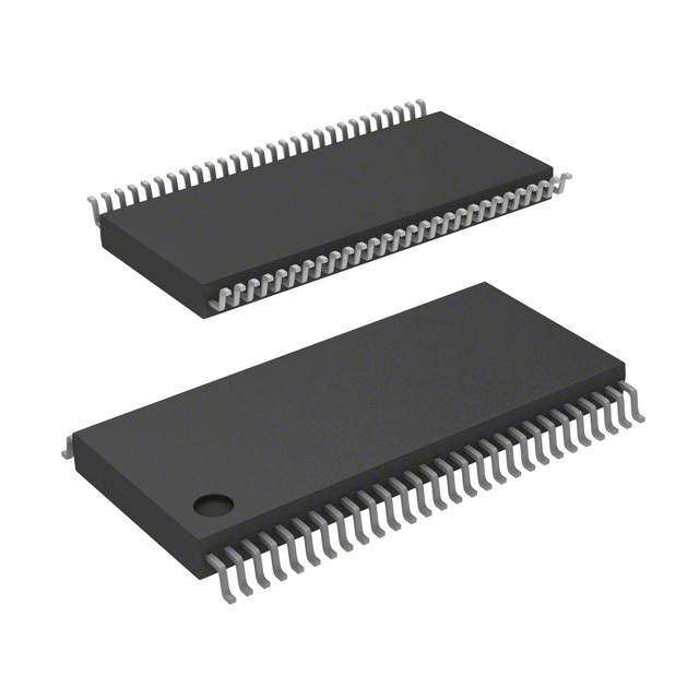
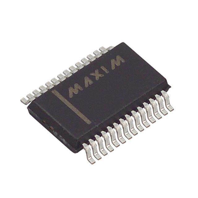
ICGOO在线商城 > 集成电路(IC) > 接口 - 驱动器,接收器,收发器 > MAX3318EIDBR
- 型号: MAX3318EIDBR
- 制造商: Texas Instruments
- 库位|库存: xxxx|xxxx
- 要求:
| 数量阶梯 | 香港交货 | 国内含税 |
| +xxxx | $xxxx | ¥xxxx |
查看当月历史价格
查看今年历史价格
MAX3318EIDBR产品简介:
ICGOO电子元器件商城为您提供MAX3318EIDBR由Texas Instruments设计生产,在icgoo商城现货销售,并且可以通过原厂、代理商等渠道进行代购。 MAX3318EIDBR价格参考。Texas InstrumentsMAX3318EIDBR封装/规格:接口 - 驱动器,接收器,收发器, 全 收发器 2/2 RS232 20-SSOP。您可以下载MAX3318EIDBR参考资料、Datasheet数据手册功能说明书,资料中有MAX3318EIDBR 详细功能的应用电路图电压和使用方法及教程。
| 参数 | 数值 |
| 产品目录 | 集成电路 (IC)半导体 |
| 描述 | IC RS232 2.5V IEC ESD 20-SSOPRS-232接口集成电路 2.5-V 460-KBPS RS-232 Transceiver |
| Duplex | Full Duplex |
| 产品分类 | |
| 品牌 | Texas Instruments |
| 产品手册 | |
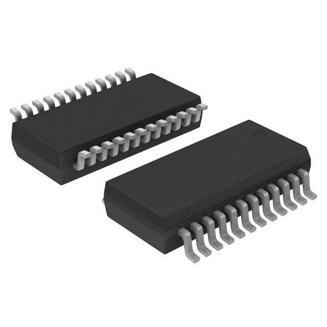
| 产品图片 |
|
| rohs | 符合RoHS无铅 / 符合限制有害物质指令(RoHS)规范要求 |
| 产品系列 | 接口 IC,RS-232接口集成电路,Texas Instruments MAX3318EIDBR- |
| 数据手册 | |
| 产品型号 | MAX3318EIDBR |
| 产品培训模块 | http://www.digikey.cn/PTM/IndividualPTM.page?site=cn&lang=zhs&ptm=7892 |
| 产品目录页面 | |
| 产品种类 | RS-232接口集成电路 |
| 传播延迟时间ns | 0.175 us |
| 供应商器件封装 | 20-SSOP |
| 关闭 | Yes |
| 其它名称 | 296-19846-6 |
| 制造商产品页 | http://www.ti.com/general/docs/suppproductinfo.tsp?distId=10&orderablePartNumber=MAX3318EIDBR |
| 功能 | Transceiver |
| 包装 | Digi-Reel® |
| 协议 | RS232 |
| 单位重量 | 156.700 mg |
| 双工 | 全 |
| 商标 | Texas Instruments |
| 安装类型 | 表面贴装 |
| 安装风格 | SMD/SMT |
| 封装 | Reel |
| 封装/外壳 | 20-SSOP(0.209",5.30mm 宽) |
| 封装/箱体 | SSOP-20 |
| 工作温度 | -40°C ~ 85°C |
| 工作温度范围 | - 40 C to + 85 C |
| 工作电源电压 | 2.5 V |
| 工厂包装数量 | 2000 |
| 接收器滞后 | 300mV |
| 接收机数量 | 2 Receiver |
| 数据速率 | 460Kbps |
| 最大工作温度 | + 85 C |
| 最小工作温度 | - 40 C |
| 标准包装 | 1 |
| 激励器数量 | 2 Driver |
| 电压-电源 | 2.25 V ~ 3 V |
| 电源电流 | 2 mA |
| 类型 | 收发器 |
| 系列 | MAX3318E |
| 输入/输出端数量 | 8 |
| 驱动器/接收器数 | 2/2 |




PDF Datasheet 数据手册内容提取
MAX3318E www.ti.com SLLS741A–JUNE2006–REVISEDOCTOBER2013 2.5-V 460-kbps RS-232 TRANSCEIVER WITH ±15-kV ESD PROTECTION CheckforSamples:MAX3318E FEATURES DESCRIPTION 1 • ESDProtectionforRS-232I/OPins The MAX3318E is a dual-driver, dual-receiver, RS- 232-compatible transceiver. The device features – ±15kV(Human-BodyModel) auto-power-down plus and enhanced electrostatic – ±8kV(IEC61000-4-2,ContactDischarge) discharge (ESD) protection integrated into the chip. – ±15kV(IEC61000-4-2,Air-GapDischarge) Driver output and receiver input are protected to ±15 kV using the IEC 61000-4-2 Air-Gap Discharge • 300-μAOperatingSupplyCurrent method, ±8 kV using the IEC 61000-4-2 Contact • 1-μALow-PowerStandby(WithReceivers Discharge method, and ±15 kV using the Human- Active)Mode BodyModel(HBM). • DesignedtoTransmitataDataRateof The device operates at a data rate of 460 kbps. The 460kbps transceiver has a proprietary low-dropout driver • Auto-Power-DownPlusOptionFeatures output stage, enabling RS-232-compatible operation FlexiblePower-SavingMode from a 2.25-V to 3-V supply with a dual charge pump. The charge pump requires only four 0.1-μF • OperatesFromaSingle2.25-Vto3-VV CC capacitors and features a logic-level output (READY) Supply that asserts when the charge pump is regulating and thedeviceisreadytobegintransmitting. APPLICATIONS The MAX3318E achieves a 1-μA supply current using • Battery-PoweredSystems the auto-power-down feature. This device • PDAs automatically enters a low-power power-down mode • CellularPhones when the RS-232 cable is disconnected or the drivers of the connected peripherals are inactive for more • Notebooks than 30 s. The device turns on again when it senses • Hand-HeldEquipment a valid transition at any driver or receiver input. Auto • Pagers power down saves power without changes to the existingBIOSoroperatingsystem. This device is available in two space-saving packages:20-pinSSOPand20-pinTSSOP. DB OR PW PACKAGE (TOP VIEW) READY 1 20 FORCEOFF C1+ 2 19 VCC V+ 3 18 GND C1− 4 17 DOUT1 C2+ 5 16 RIN1 C2− 6 15 ROUT1 V− 7 14 FORCEON DOUT2 8 13 DIN1 RIN2 9 12 DIN2 ROUT2 10 11 INVALID 1 Pleasebeawarethatanimportantnoticeconcerningavailability,standardwarranty,anduseincriticalapplicationsof TexasInstrumentssemiconductorproductsanddisclaimerstheretoappearsattheendofthisdatasheet. PRODUCTIONDATAinformationiscurrentasofpublicationdate. Copyright©2006–2013,TexasInstrumentsIncorporated Products conform to specifications per the terms of the Texas Instruments standard warranty. Production processing does not necessarilyincludetestingofallparameters.
MAX3318E SLLS741A–JUNE2006–REVISEDOCTOBER2013 www.ti.com This integrated circuit can be damaged by ESD. Texas Instruments recommends that all integrated circuits be handled with appropriateprecautions.Failuretoobserveproperhandlingandinstallationprocedurescancausedamage. ESDdamagecanrangefromsubtleperformancedegradationtocompletedevicefailure.Precisionintegratedcircuitsmaybemore susceptibletodamagebecauseverysmallparametricchangescouldcausethedevicenottomeetitspublishedspecifications. DETAILED DESCRIPTION Flexible control options for power management are featured when the serial port and driver inputs are inactive. The auto-power-down plus feature functions when FORCEON is low and FORCEOFF is high. During this mode of operation, if the device does not sense valid signal transitions on all receiver and driver inputs for approximately 30 s, the built-in charge pump and drivers are powered down, reducing the supply current to 1 μA. Bydisconnectingtheserialportorplacingtheperipheraldriversoff,auto-power-downpluscanbedisabledwhen FORCEON and FORCEOFF are high. With auto-power-down plus enabled, the device activates automatically when a valid signal is applied to any receiver or driver input. INVALID is high (valid data) if any receiver input voltage is greater than 2.7 V or less than –2.7 V, or has been between –0.3 V and 0.3 V for less than 30 μs (typical number). INVALID is low (invalid data) if all receiver input voltage are between –0.3 V and 0.3 V for more than30μs(typicalnumber). FUNCTIONTABLE(1) INPUTCONDITIONS OUTPUTSTATES VALID RECEIVER RS-232 OPERATING FORCEON FORCEOFF ORDRIVER LEVEL DRIVER RECEIVER INVALID READY MODE EDGE PRESENTAT WITHIN30s RECEIVER Auto-Power-DownPlusConditions Normaloperation, H H No No Active Active L H auto-power-down plusdisabled Normaloperation, H H No Yes Active Active H H auto-power-down plusdisabled Normaloperation, L H Yes No Active Active L H auto-power-down plusenabled Normaloperation, L H Yes Yes Active Active H H auto-power-down plusenabled Powerdown, L H No No Z Active L L auto-power-down plusenabled Powerdown, L H No Yes Z Active H L auto-power-down plusenabled Manualpower X L X No Z Active L L down Manualpower X L X Yes Z Active H L down Auto-Power-DownConditions Powerdown,auto INVALID INVALID X No Z Active L L powerdown enabled Normaloperation, INVALID INVALID X Yes Active Active H H autopowerdown enabled (1) H=highlevel,L=lowlevel,X=irrelevant,Z=highimpedance 2 SubmitDocumentationFeedback Copyright©2006–2013,TexasInstrumentsIncorporated ProductFolderLinks:MAX3318E
MAX3318E www.ti.com SLLS741A–JUNE2006–REVISEDOCTOBER2013 LOGICDIAGRAM(POSITIVELOGIC) 13 17 DIN1 DOUT1 12 8 DIN2 DOUT2 20 11 FORCEOFF INVALID Auto-Power-Down Plus 14 1 FORCEON READY 15 16 ROUT1 RIN1 5 kW 10 9 ROUT2 RIN2 5 kW TERMINALFUNCTIONS TERMINAL DESCRIPTION NAME NO. C1+ 2 Positivevoltage-doublercharge-pumpcapacitor C1– 4 Negativevoltage-doublercharge-pumpcapacitor C2+ 5 Positiveinvertingcharge-pumpcapacitor C2– 6 Negativeinvertingcharge-pumpcapacitor DIN 12,13 CMOSdriverinputs DOUT 8,17 RS-232driveroutputs Force-offinput,activelow.Drivelowtopowerdowntransmittersandchargepump.Thisoverridesautopower FORCEOFF 20 downandFORCEON(seeFunctionTable). Force-oninput,activehigh.Drivehightooverrideautopowerdown,keepingtransmitterson(FORCEOFF FORCEON 14 mustbehigh)(seeFunctionTable). GND 18 Ground Validsignaldetectoroutput,activelow.AlogichighindicatesthatavalidRS-232levelispresentonareceiver INVALID 11 input. Readytotransmitoutput,activehigh.READYisenabledhighwhenV–goesbelow–3.5Vandthedeviceis READY 1 readytotransmit. RIN 9,16 RS-232receiverinputs ROUT 10,15 CMOSreceiveroutputs V+ 3 2×V generatedbythechargepump CC V– 7 –2×V generatedbythechargepump CC V 19 2.25-Vto3-Vsingle-supplyvoltage CC Copyright©2006–2013,TexasInstrumentsIncorporated SubmitDocumentationFeedback 3 ProductFolderLinks:MAX3318E
MAX3318E SLLS741A–JUNE2006–REVISEDOCTOBER2013 www.ti.com Absolute Maximum Ratings(1) overoperatingfree-airtemperaturerange(unlessotherwisenoted) MIN MAX UNIT V toGND –0.3 6 V CC V+toGND(2) –0.3 7 V V–toGND(2) –7 0.3 V V++IV-I(2) 13 V DIN,FORCEON,FORCEOFFtoGND –0.3 6 Inputvoltage V RINtoGND ±25 DOUTtoGND ±13.2 Outputvoltage V ROUT,INVALID,READYtoGND –0.3 V +0.3 CC Short-circuitduration DOUTtoGND Continuous 16-pinSSOP(derate7.14mW/°Cabove70°C) 571 Continuouspowerdissipation(T =70°C) 20-pinSSOP(derate8mW/°Cabove70°C 640 mW A 20-pinTSSOP(derate7mW/°Cabove70°C) 559 Storagetemperaturerange –65 150 °C Leadtemperature(soldering,10s) 300 °C (1) Stressesbeyondthoselistedunder"absolutemaximumratings"maycausepermanentdamagetothedevice.Thesearestressratings only,andfunctionaloperationofthedeviceattheseoranyotherconditionsbeyondthoseindicatedunder"recommendedoperating conditions"isnotimplied.Exposuretoabsolute-maximum-ratedconditionsforextendedperiodsmayaffectdevicereliability. (2) V+andV–canhavemaximummagnitudesof7V,buttheirabsolutedifferencecannotexceed13V. Recommended Operating Conditions SeeFigure4 MIN NOM MAX UNIT Supplyvoltage 2.25 2.5 3 V DIN,FORCEOFF, V Driverandcontrolhigh-levelinputvoltage V =2.5Vto3V 0.7×V 5.5 V IH FORCEON CC CC DIN,FORCEOFF, V Driverandcontrollow-levelinputvoltage V =2.5Vto3V 0 0.3×V V IL FORCEON CC CC V Receiverinputvoltage –25 25 V I MAX3318EC 0 70 T Operatingfree-airtemperature °C A MAX3318EI –40 85 4 SubmitDocumentationFeedback Copyright©2006–2013,TexasInstrumentsIncorporated ProductFolderLinks:MAX3318E
MAX3318E www.ti.com SLLS741A–JUNE2006–REVISEDOCTOBER2013 Supply Current Section Electrical Characteristics V =2.25Vto3V,C1–C4=0.1μF,T =T toT (unlessotherwisenoted) CC A MIN MAX PARAMETER TESTCONDITIONS MIN TYP(1) MAX UNIT DCCharacteristics(V =2.5V,T =25°C) CC A Auto-power-downplussupplycurrent FORCEON=GND,FORCEOFF=V ,AllRINandDINidle 1 10 μA CC Auto-power-downsupplycurrent FORCEOFF=GND 1 10 μA Supplycurrent FORCEON=FORCEOFF=V ,Noload 0.3 2 mA CC (1) TypicalvaluesareatV =2.5V,T =25°C. CC A ESD Protection PARAMETER TESTCONDITIONS TYP UNIT HBM ±15 RIN,DOUT IEC61000-4-2Air-GapDischargemethod ±15 kV IEC61000-4-2ContactDischargemethod ±8 Driver Section Electrical Characteristics overrecommendedrangesofsupplyvoltageandoperatingfree-airtemperature, V =2.25Vto3V,C1–C4=0.1μF,T =T toT (unlessotherwisenoted)(seeFigure4) CC A MIN MAX PARAMETER TESTCONDITIONS MIN TYP(1) MAX UNIT Driverinputhysteresis 0.3 V Inputleakagecurrent FORCEON,DIN,FORCEOFF ±0.01 ±1 μA Outputvoltageswing Alldriveroutputsloadedwith3kΩtoground ±3.7 ±4 V Outputresistance V =0,Driveroutput=±2V 300 10M Ω CC Outputshort-circuitcurrent(2) ±25 ±60 mA Outputleakagecurrent V =0or2.25Vto3V,V =±12V,Driversdisabled ±25 μA CC OUT (1) TypicalvaluesareatV =2.5V,T =25°C. CC A (2) Short-circuitdurationsshouldbecontrolledtopreventexceedingthedeviceabsolutepowerdissipationratings,andnotmorethanone outputshouldbeshortedatatime. Driver Section Switching Characteristics overrecommendedrangesofsupplyvoltageandoperatingfree-airtemperature, V =2.25Vto3V,C1–C4=0.1μF,T =T toT (unlessotherwisenoted)(seeFigure1) CC A MIN MAX PARAMETER TESTCONDITIONS MIN TYP(1) MAX UNIT Maximumdatarate R =3kΩ,C =1000pF,Onetransmitterswitching 460 kbps L L |t –t | Driverskew(2) 100 ns PHL PLH V =2.5V,T =25°C,R =3kΩto7kΩ, CC A L Transition-regionslewrate Measuredfrom3Vto–3Vor–3Vto3V, 4 30 V/μs C =150pFto2500pF L (1) TypicalvaluesareatV =2.5V,T =25°C. CC A (2) Pulseskewisdefinedas|t –t |ofeachchannelofthesamedevice. PLH PHL Copyright©2006–2013,TexasInstrumentsIncorporated SubmitDocumentationFeedback 5 ProductFolderLinks:MAX3318E
MAX3318E SLLS741A–JUNE2006–REVISEDOCTOBER2013 www.ti.com Receiver Section Electrical Characteristics overrecommendedrangesofsupplyvoltageandoperatingfree-airtemperature, V =2.25Vto3V,C1–C4=0.1μF,T =T toT (unlessotherwisenoted)(seeFigure4) CC A MIN MAX PARAMETER TESTCONDITIONS MIN TYP(1) MAX UNIT Inputvoltagerange –25 25 V Inputthresholdlow T =25°C 0.3×V V A CC Inputthresholdhigh T =25°C 0.7×V V A CC Inputhysteresis 0.3 V Inputresistance T =25°C 3 5 7 kΩ A Outputleakagecurrent ±0.05 ±10 μA Outputvoltagelow I =0.5mA 0.1×V V OUT CC Outputvoltagehigh I =–0.5mA 0.9×V V OUT CC (1) TypicalvaluesareatV =2.5V,T =25°C. CC A Receiver Section Switching Characteristics overrecommendedrangesofsupplyvoltageandoperatingfree-airtemperature, V =2.25Vto3V,C1–C4=0.1μF,T =T toT (unlessotherwisenoted)(seeFigure4) CC A MIN MAX PARAMETER TESTCONDITIONS TYP(1) UNIT t 0.175 PHL Receiverpropagationdelay RINtoROUT,C =150pF μs L t 0.175 PLH |t –t | Receiverskew(2) 50 ns PHL PLH (1) TypicalvaluesareatV =2.5V,T =25°C. CC A (2) Pulseskewisdefinedas|t –t |ofeachchannelofthesamedevice. PLH PHL Auto-Power-Down Plus Section Electrical Characteristics overrecommendedrangesofsupplyvoltageandoperatingfree-airtemperature, V =2.25Vto3V,C1–C4=0.1μF,T =T toT (unlessotherwisenoted)(seeFigure4) CC A MIN MAX PARAMETER TESTCONDITIONS MIN MAX UNIT Positivethreshold 2.7 ReceiverinputthresholdtoINVALIDhigh V Negativethreshold –2.7 ReceiverinputthresholdINVALIDlow –0.3 0.3 V INVALID,READYvoltagelow I =0.5mA 0.1×V V OUT CC INVALID,READYvoltagehigh I =–0.5mA 0.8×V V OUT CC Auto-Power-Down Plus Section Switching Characteristics overrecommendedrangesofsupplyvoltageandoperatingfree-airtemperature, V =2.25Vto3V,C1–C4=0.1μF,T =T toT (unlessotherwisenoted)(seeFigure4) CC A MIN MAX PARAMETER TESTCONDITIONS MIN TYP(1) MAX UNIT t ReceiverpositiveornegativethresholdtoINVALIDhigh V =2.5V 1 μs INVH CC t ReceiverpositiveornegativethresholdtoINVALIDlow V =2.5V 30 μs INVL CC t Receiverordriveredgetodriverenabled V =2.5V 100 μs WU CC t Receiverordriveredgetodrivershutdown V =2.5V 15 30 60 s AUTOPRDN CC (1) TypicalvaluesareatV =2.5V,T =25°C. CC A 6 SubmitDocumentationFeedback Copyright©2006–2013,TexasInstrumentsIncorporated ProductFolderLinks:MAX3318E
MAX3318E www.ti.com SLLS741A–JUNE2006–REVISEDOCTOBER2013 PARAMETER MEASUREMENT INFORMATION 3 V RS-232 Input Output 0 V Generator 50 W (see Note B) RL C(sLe e Note A) tTHL tTLH 3 V 3 V 3 V VOH Output FORCEOFF −3 V −3 V VOL SR(tr)(cid:1) 6V t ort TEST CIRCUIT THL TLH VOLTAGE WAVEFORMS NOTES: A. CL includes probe and jig capacitance. B. The pulse generator has the following characteristics: PRR = 250 kbit/s, ZO = 50 W , 50% duty cycle, tr ≤ 10 ns, tf ≤ 10 ns. Figure1.DriverSlewRate 2.25 V RS-232 Input 1.125 V 1.125 V Output 0 V Generator 50 W (see Note B) RL C(sLe e Note A) tPHL tPLH VOH 3 V Output 50% 50% FORCEOFF VOL TEST CIRCUIT VOLTAGE WAVEFORMS NOTES: A. CL includes probe and jig capacitance. B. The pulse generator has the following characteristics: PRR = 250 kbit/s, ZO = 50 W , 50% duty cycle, tr ≤ 10 ns, tf ≤ 10 ns. Figure2.DriverPulseSkew 3 V Input 0 V 0 V −3 V Output Generator 50 W tPHL tPLH (see Note B) CL (see Note A) VOH Output 50% 50% VOL TEST CIRCUIT VOLTAGE WAVEFORMS NOTES: A. CL includes probe and jig capacitance. B. The pulse generator has the following characteristics: ZO = 50 W , 50% duty cycle, tr ≤ 10 ns, tf ≤ 10 ns. Figure3.ReceiverPropagationDelayTimes Copyright©2006–2013,TexasInstrumentsIncorporated SubmitDocumentationFeedback 7 ProductFolderLinks:MAX3318E
MAX3318E SLLS741A–JUNE2006–REVISEDOCTOBER2013 www.ti.com PARAMETER MEASUREMENT INFORMATION Receiver } Invalid Inputs Region Driver Inputs Driver Outputs INVALID VCC Output tINVL tINVH 0 tWU tWU VCC Ready 0 Output V+ VCC 0 V− VOLTAGE WAVEFORMS ÎÎVÎalidÎ RS-Î232Î LevÎel, INÎVALÎID HÎighÎÎ ROUT 2.7 ÎV ÎÎÎÎÎÎÎÎÎÎÎ Generator (see Note B) 50 W ÎÎÎÎÎIndeÎtermÎinatÎe ÎÎÎÎ 0.3 V ÎÎÎÎÎÎÎÎÎÎÎÎÎÎÎÎÎÎÎÎÎÎÎÎ If Signal Remains Within This Region 0 ÎV ÎFoÎr MoÎre TÎhan Î30 m Îs, INÎVALÎID IsÎ LowΆ Î −0.3 V ÎÎÎÎÎÎÎÎÎÎÎÎ Indeterminate Auto-Power- INVALID ÎÎÎÎÎÎÎÎÎÎÎÎ Down Plus −2.7 V CL = 30 pF ÎÎÎÎÎÎÎÎÎÎÎÎ Valid RS-232 Level, INVALID High (see Note A) FORCEON †Auto power down disables drivers and reduces supply current to 1 m A. DIN DOUT FORCEOFF TEST CIRCUIT Figure4. INVALID PropagationDelayTimesandSupplyEnablingTime 8 SubmitDocumentationFeedback Copyright©2006–2013,TexasInstrumentsIncorporated ProductFolderLinks:MAX3318E
MAX3318E www.ti.com SLLS741A–JUNE2006–REVISEDOCTOBER2013 PARAMETER MEASUREMENT INFORMATION 2.5 V + 0.1 (cid:1)F 19 CBYPASS 2 VCC 3 + C1+ V+ + C1 C3 4 0.1 (cid:1)F C1− 0.1 (cid:1)F 5 7 + C2+ V− C2 C4 6 + 0.1 (cid:1)F C2− 0.1 (cid:1)F 13 DIN1 DOUT1 17 RS-232-Compatible Outputs 12DIN2 DOUT2 8 15ROUT1 RRIINN11 16 RS-232-Compatible Inputs 5k 10ROUT2 RIN2 9 5k 1 READY To Power-Management Unit Auto-Power- INVALID 11 Down Plus VCC 14 FORCEOFF 20 FORCEON GND 18 Figure5.TypicalApplicationCircuit Copyright©2006–2013,TexasInstrumentsIncorporated SubmitDocumentationFeedback 9 ProductFolderLinks:MAX3318E
MAX3318E SLLS741A–JUNE2006–REVISEDOCTOBER2013 www.ti.com REVISION HISTORY ChangesfromOriginal(June2006)toRevisionA Page • UpdateddocumenttonewTIdatasheetformat-nospecificationchanges. ....................................................................... 1 • RemovedOrderingInformationTable. ................................................................................................................................. 2 • UpdatedTERMINALFUNCTIONStabletofixinconsistency. .............................................................................................. 3 10 SubmitDocumentationFeedback Copyright©2006–2013,TexasInstrumentsIncorporated ProductFolderLinks:MAX3318E
PACKAGE OPTION ADDENDUM www.ti.com 6-Feb-2020 PACKAGING INFORMATION Orderable Device Status Package Type Package Pins Package Eco Plan Lead/Ball Finish MSL Peak Temp Op Temp (°C) Device Marking Samples (1) Drawing Qty (2) (6) (3) (4/5) MAX3318ECDBR ACTIVE SSOP DB 20 2000 Green (RoHS NIPDAU Level-1-260C-UNLIM 0 to 70 MP318EC & no Sb/Br) MAX3318ECPW ACTIVE TSSOP PW 20 70 Green (RoHS NIPDAU Level-1-260C-UNLIM 0 to 70 MP318EC & no Sb/Br) MAX3318ECPWR ACTIVE TSSOP PW 20 2000 Green (RoHS NIPDAU Level-1-260C-UNLIM 0 to 70 MP318EC & no Sb/Br) MAX3318EIDB ACTIVE SSOP DB 20 70 Green (RoHS NIPDAU Level-1-260C-UNLIM -40 to 85 MP318EI & no Sb/Br) MAX3318EIDBG4 ACTIVE SSOP DB 20 70 Green (RoHS NIPDAU Level-1-260C-UNLIM -40 to 85 MP318EI & no Sb/Br) MAX3318EIDBR ACTIVE SSOP DB 20 2000 Green (RoHS NIPDAU Level-1-260C-UNLIM -40 to 85 MP318EI & no Sb/Br) MAX3318EIPW ACTIVE TSSOP PW 20 70 Green (RoHS NIPDAU Level-1-260C-UNLIM -40 to 85 MP318EI & no Sb/Br) MAX3318EIPWR ACTIVE TSSOP PW 20 2000 Green (RoHS NIPDAU Level-1-260C-UNLIM -40 to 85 MP318EI & no Sb/Br) MAX3318EIPWRG4 ACTIVE TSSOP PW 20 2000 Green (RoHS NIPDAU Level-1-260C-UNLIM -40 to 85 MP318EI & no Sb/Br) (1) The marketing status values are defined as follows: ACTIVE: Product device recommended for new designs. LIFEBUY: TI has announced that the device will be discontinued, and a lifetime-buy period is in effect. NRND: Not recommended for new designs. Device is in production to support existing customers, but TI does not recommend using this part in a new design. PREVIEW: Device has been announced but is not in production. Samples may or may not be available. OBSOLETE: TI has discontinued the production of the device. (2) RoHS: TI defines "RoHS" to mean semiconductor products that are compliant with the current EU RoHS requirements for all 10 RoHS substances, including the requirement that RoHS substance do not exceed 0.1% by weight in homogeneous materials. Where designed to be soldered at high temperatures, "RoHS" products are suitable for use in specified lead-free processes. TI may reference these types of products as "Pb-Free". RoHS Exempt: TI defines "RoHS Exempt" to mean products that contain lead but are compliant with EU RoHS pursuant to a specific EU RoHS exemption. Green: TI defines "Green" to mean the content of Chlorine (Cl) and Bromine (Br) based flame retardants meet JS709B low halogen requirements of <=1000ppm threshold. Antimony trioxide based flame retardants must also meet the <=1000ppm threshold requirement. (3) MSL, Peak Temp. - The Moisture Sensitivity Level rating according to the JEDEC industry standard classifications, and peak solder temperature. Addendum-Page 1
PACKAGE OPTION ADDENDUM www.ti.com 6-Feb-2020 (4) There may be additional marking, which relates to the logo, the lot trace code information, or the environmental category on the device. (5) Multiple Device Markings will be inside parentheses. Only one Device Marking contained in parentheses and separated by a "~" will appear on a device. If a line is indented then it is a continuation of the previous line and the two combined represent the entire Device Marking for that device. (6) Lead/Ball Finish - Orderable Devices may have multiple material finish options. Finish options are separated by a vertical ruled line. Lead/Ball Finish values may wrap to two lines if the finish value exceeds the maximum column width. Important Information and Disclaimer:The information provided on this page represents TI's knowledge and belief as of the date that it is provided. TI bases its knowledge and belief on information provided by third parties, and makes no representation or warranty as to the accuracy of such information. Efforts are underway to better integrate information from third parties. TI has taken and continues to take reasonable steps to provide representative and accurate information but may not have conducted destructive testing or chemical analysis on incoming materials and chemicals. TI and TI suppliers consider certain information to be proprietary, and thus CAS numbers and other limited information may not be available for release. In no event shall TI's liability arising out of such information exceed the total purchase price of the TI part(s) at issue in this document sold by TI to Customer on an annual basis. Addendum-Page 2
PACKAGE MATERIALS INFORMATION www.ti.com 11-Oct-2013 TAPE AND REEL INFORMATION *Alldimensionsarenominal Device Package Package Pins SPQ Reel Reel A0 B0 K0 P1 W Pin1 Type Drawing Diameter Width (mm) (mm) (mm) (mm) (mm) Quadrant (mm) W1(mm) MAX3318ECDBR SSOP DB 20 2000 330.0 16.4 8.2 7.5 2.5 12.0 16.0 Q1 MAX3318ECPWR TSSOP PW 20 2000 330.0 16.4 6.95 7.1 1.6 8.0 16.0 Q1 MAX3318EIDBR SSOP DB 20 2000 330.0 16.4 8.2 7.5 2.5 12.0 16.0 Q1 MAX3318EIPWR TSSOP PW 20 2000 330.0 16.4 6.95 7.1 1.6 8.0 16.0 Q1 PackMaterials-Page1
PACKAGE MATERIALS INFORMATION www.ti.com 11-Oct-2013 *Alldimensionsarenominal Device PackageType PackageDrawing Pins SPQ Length(mm) Width(mm) Height(mm) MAX3318ECDBR SSOP DB 20 2000 367.0 367.0 38.0 MAX3318ECPWR TSSOP PW 20 2000 367.0 367.0 38.0 MAX3318EIDBR SSOP DB 20 2000 367.0 367.0 38.0 MAX3318EIPWR TSSOP PW 20 2000 367.0 367.0 38.0 PackMaterials-Page2
None
None
PACKAGE OUTLINE DB0020A SSOP - 2 mm max height SCALE 2.000 SMALL OUTLINE PACKAGE C 8.2 TYP 7.4 A 0.1 C PIN 1 INDEX AREA SEATING PLANE 18X 0.65 20 1 2X 7.5 5.85 6.9 NOTE 3 10 11 0.38 20X 0.22 5.6 B 0.1 C A B 5.0 NOTE 4 2 MAX (0.15) TYP 0.25 SEE DETAIL A GAGE PLANE 0 -8 0.95 0.05 MIN 0.55 DETA 15AIL A TYPICAL 4214851/B 08/2019 NOTES: 1. All linear dimensions are in millimeters. Any dimensions in parenthesis are for reference only. Dimensioning and tolerancing per ASME Y14.5M. 2. This drawing is subject to change without notice. 3. This dimension does not include mold flash, protrusions, or gate burrs. Mold flash, protrusions, or gate burrs shall not exceed 0.15 mm per side. 4. This dimension does not include interlead flash. Interlead flash shall not exceed 0.25 mm per side. 5. Reference JEDEC registration MO-150. www.ti.com
EXAMPLE BOARD LAYOUT DB0020A SSOP - 2 mm max height SMALL OUTLINE PACKAGE 20X (1.85) SYMM (R0.05) TYP 1 20X (0.45) 20 SYMM 18X (0.65) 10 11 (7) LAND PATTERN EXAMPLE EXPOSED METAL SHOWN SCALE: 10X SOLDER MASK METAL METAL UNDER SOLDER MASK OPENING SOLDER MASK OPENING EXPOSED METAL EXPOSED METAL 0.07 MAX 0.07 MIN ALL AROUND ALL AROUND NON-SOLDER MASK SOLDER MASK DEFINED DEFINED (PREFERRED) SOLDE15.000 R MASK DETAILS 4214851/B 08/2019 NOTES: (continued) 6. Publication IPC-7351 may have alternate designs. 7. Solder mask tolerances between and around signal pads can vary based on board fabrication site. www.ti.com
EXAMPLE STENCIL DESIGN DB0020A SSOP - 2 mm max height SMALL OUTLINE PACKAGE 20X (1.85) SYMM (R0.05) TYP 1 20X (0.45) 20 SYMM 18X (0.65) 10 11 (7) SOLDER PASTE EXAMPLE BASED ON 0.125 mm THICK STENCIL SCALE: 10X 4214851/B 08/2019 NOTES: (continued) 8. Laser cutting apertures with trapezoidal walls and rounded corners may offer better paste release. IPC-7525 may have alternate design recommendations. 9. Board assembly site may have different recommendations for stencil design. www.ti.com
IMPORTANTNOTICEANDDISCLAIMER TI PROVIDES TECHNICAL AND RELIABILITY DATA (INCLUDING DATASHEETS), DESIGN RESOURCES (INCLUDING REFERENCE DESIGNS), APPLICATION OR OTHER DESIGN ADVICE, WEB TOOLS, SAFETY INFORMATION, AND OTHER RESOURCES “AS IS” AND WITH ALL FAULTS, AND DISCLAIMS ALL WARRANTIES, EXPRESS AND IMPLIED, INCLUDING WITHOUT LIMITATION ANY IMPLIED WARRANTIES OF MERCHANTABILITY, FITNESS FOR A PARTICULAR PURPOSE OR NON-INFRINGEMENT OF THIRD PARTY INTELLECTUAL PROPERTY RIGHTS. These resources are intended for skilled developers designing with TI products. You are solely responsible for (1) selecting the appropriate TI products for your application, (2) designing, validating and testing your application, and (3) ensuring your application meets applicable standards, and any other safety, security, or other requirements. These resources are subject to change without notice. TI grants you permission to use these resources only for development of an application that uses the TI products described in the resource. Other reproduction and display of these resources is prohibited. No license is granted to any other TI intellectual property right or to any third party intellectual property right. TI disclaims responsibility for, and you will fully indemnify TI and its representatives against, any claims, damages, costs, losses, and liabilities arising out of your use of these resources. TI’s products are provided subject to TI’s Terms of Sale (www.ti.com/legal/termsofsale.html) or other applicable terms available either on ti.com or provided in conjunction with such TI products. TI’s provision of these resources does not expand or otherwise alter TI’s applicable warranties or warranty disclaimers for TI products. Mailing Address: Texas Instruments, Post Office Box 655303, Dallas, Texas 75265 Copyright © 2020, Texas Instruments Incorporated

 Datasheet下载


