ICGOO在线商城 > 集成电路(IC) > 接口 - 驱动器,接收器,收发器 > MAX3227IDB
 Datasheet下载
- 型号: MAX3227IDB
- 制造商: Texas Instruments
- 库位|库存: xxxx|xxxx
- 要求:
| 数量阶梯 | 香港交货 | 国内含税 |
| +xxxx | $xxxx | ¥xxxx |
查看当月历史价格
查看今年历史价格
MAX3227IDB产品简介:
ICGOO电子元器件商城为您提供MAX3227IDB由Texas Instruments设计生产,在icgoo商城现货销售,并且可以通过原厂、代理商等渠道进行代购。 MAX3227IDB价格参考¥5.65-¥11.46。Texas InstrumentsMAX3227IDB封装/规格:接口 - 驱动器,接收器,收发器, 全 收发器 1/1 RS232 16-SSOP。您可以下载MAX3227IDB参考资料、Datasheet数据手册功能说明书,资料中有MAX3227IDB 详细功能的应用电路图电压和使用方法及教程。
| 参数 | 数值 |
| 产品目录 | 集成电路 (IC)半导体 |
| 描述 | IC RS232 3V5.5V 15KVESD 16-SSOPRS-232接口集成电路 3 to 5.5V Single Ch RS-232 Line Drv/Rcvr |
| Duplex | Full Duplex |
| 产品分类 | |
| 品牌 | Texas Instruments |
| 产品手册 | |
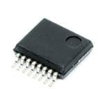
| 产品图片 |
|
| rohs | 符合RoHS无铅 / 符合限制有害物质指令(RoHS)规范要求 |
| 产品系列 | 接口 IC,RS-232接口集成电路,Texas Instruments MAX3227IDB- |
| 数据手册 | |
| 产品型号 | MAX3227IDB |
| 产品种类 | RS-232接口集成电路 |
| 传播延迟时间ns | 0.15 us |
| 供应商器件封装 | 16-SSOP |
| 关闭 | Yes |
| 其它名称 | 296-33383-5 |
| 功能 | Transceiver |
| 包装 | 管件 |
| 协议 | RS232 |
| 单位重量 | 128.600 mg |
| 双工 | 全 |
| 商标 | Texas Instruments |
| 安装类型 | 表面贴装 |
| 安装风格 | SMD/SMT |
| 封装 | Tube |
| 封装/外壳 | 16-SSOP(0.209",5.30mm 宽) |
| 封装/箱体 | SSOP-16 |
| 工作温度 | -40°C ~ 85°C |
| 工作温度范围 | - 40 C to + 85 C |
| 工作电源电压 | 3 V to 5.5 V |
| 工厂包装数量 | 80 |
| 接收器滞后 | 500mV |
| 接收机数量 | 1 Receiver |
| 数据速率 | 1Mbps |
| 最大工作温度 | + 85 C |
| 最小工作温度 | - 40 C |
| 标准包装 | 80 |
| 激励器数量 | 1 Driver |
| 电压-电源 | 3 V ~ 5.5 V |
| 电源电流 | 2 mA |
| 类型 | 收发器 |
| 系列 | MAX3227 |
| 输入/输出端数量 | 4 |
| 驱动器/接收器数 | 1/1 |


- 商务部:美国ITC正式对集成电路等产品启动337调查
- 曝三星4nm工艺存在良率问题 高通将骁龙8 Gen1或转产台积电
- 太阳诱电将投资9.5亿元在常州建新厂生产MLCC 预计2023年完工
- 英特尔发布欧洲新工厂建设计划 深化IDM 2.0 战略
- 台积电先进制程称霸业界 有大客户加持明年业绩稳了
- 达到5530亿美元!SIA预计今年全球半导体销售额将创下新高
- 英特尔拟将自动驾驶子公司Mobileye上市 估值或超500亿美元
- 三星加码芯片和SET,合并消费电子和移动部门,撤换高东真等 CEO
- 三星电子宣布重大人事变动 还合并消费电子和移动部门
- 海关总署:前11个月进口集成电路产品价值2.52万亿元 增长14.8%


PDF Datasheet 数据手册内容提取
MAX3227 3-V TO 5.5-V SINGLE-CHANNEL RS-232 LINE DRIVER/RECEIVER WITH – 15-kV ESD PROTECTION www.ti.com SLLS673A–AUGUST2005–REVISEDFEBRUARY2006 FEATURES APPLICATIONS • MeetsorExceedstheRequirementsof • Battery-Powered,Hand-Held,andPortable TIA/EIA-232-FandITUv.28Standards Equipment • OperatesWith3-Vto5.5-VV Supply • PDAsandPalmtopPCs CC • OperatesatLeast1Mbit/s • Notebooks,Sub-Notebooks,andLaptops • LowStandbyCurrent...1m ATyp • DigitalCameras • MobilePhonesandWirelessDevices • ExternalCapacitors...4· 0.1m F • Accepts5-VLogicInputWith3.3-VSupply DB PACKAGE • DesignedtoBeInterchangeableWithMaxim™ (TOP VIEW) MAX3227 READY 1 16 FORCEOFF • Latch-UpPerformanceExceeds100mAPer JESD78,ClassII C1+ 2 15 VCC V+ 3 14 GND • ESDProtectionforRS-232I/OPins C1− 4 13 DOUT – – 15kV–Human-BodyModel C2+ 5 12 FORCEON – – 8kV–IEC61000-4-2,ContactDischarge C2− 6 11 DIN – – 8kV–IEC61000-4-2,Air-GapDischarge V− 7 10 INVALID • Auto-PowerdownPlusFeatureAutomatically RIN 8 9 ROUT DisablesDriversforPowerSavings • PackagedinPlasticShrinkSmall-Outline Package DESCRIPTION/ORDERING INFORMATION The MAX3227 consists of one line driver, one line receiver, and a dual charge-pump circuit with – 15-kV ESD protection pin to pin (serial-port connection pins, including GND). The device meets the requirements of TIA/EIA-232-F and provides the electrical interface between an asynchronous communication controller and the serial-port connector. The charge pump and four small external capacitors allow operation from a single 3-V to 5.5-V supply. This device operates at data-signaling rates of 1 Mbit/s in normal operating mode and a maximum of 30-V/m s driver output slew rate. This device also features a logic-level output (READY) that asserts when the chargepumpisregulatingandthedeviceisreadytobegintransmitting. The MAX3227 achieves a 1-m A supply current using the auto-powerdown plus feature. This device automatically enters a low-power powerdown mode when the RS-232 cable is disconnected or the drivers of the connected peripheralsareinactiveformorethan30s.Theyturnonagainwhenthey sense a valid transition at any driver or receiverinput.Auto-powerdownsavespowerwithoutchangestotheexistingBIOSoroperatingsystem. The MAX3227C is characterized for operation from 0(cid:176) C to 70(cid:176) C. The MAX3227I is characterized for operation from–40(cid:176) Cto85(cid:176) C. AVAILABLEOPTIONS PACKAGEDDEVICE TA SHRINKSMALLOUTLINE (DB)(1) 0(cid:176) Cto70(cid:176) C MAX3227CDB –40(cid:176) Cto85(cid:176) C MAX3227IDB (1) TheDBpackageisavailabletapedandreeled.AddthesuffixRto devicetype(e.g.,MAX3227CDBR). Pleasebeawarethatanimportantnoticeconcerningavailability,standardwarranty,anduseincriticalapplicationsofTexas Instrumentssemiconductorproductsanddisclaimerstheretoappearsattheendofthisdatasheet. Alltrademarksarethepropertyoftheirrespectiveowners. PRODUCTIONDATAinformationiscurrentasofpublicationdate. Copyright©2005–2006,TexasInstrumentsIncorporated Products conform to specifications per the terms of the Texas Instruments standard warranty. Production processing does not necessarilyincludetestingofallparameters.
MAX3227 3-V TO 5.5-V SINGLE-CHANNEL RS-232 LINE DRIVER/RECEIVER WITH – 15-kV ESD PROTECTION www.ti.com SLLS673A–AUGUST2005–REVISEDFEBRUARY2006 FUNCTIONTABLE(1) INPUTCONDITIONS OUTPUTSTATES RECEIVER VALID OR DRIVER RS-232 OPERATINGMODE FORCEON FORCEOFF LEVEL DRIVER RECEIVER INVALID READY EDGE PRESENTAT WITHIN RECEIVER 30s Auto-PowerdownPlusConditions Normaloperation, H H NO NO Active Active L H auto-powerdownplusdisabled Normaloperation, H H NO YES Active Active H H auto-powerdownplusdisabled Normaloperation, L H YES NO Active Active L H auto-powerdownplusenabled Normaloperation, L H YES YES Active Active H H auto-powerdownplusenabled Powerdown, L H NO NO Z Active L L auto-powerdownplusenabled Powerdown, L H NO YES Z Active H L auto-powerdownplusenabled X L X NO Z Active L L Manualpowerdown X L X YES Z Active H L Manualpowerdown Auto-PowerdownConditions Powerdown, INVALID INVALID X NO Z Active L L auto-powerdownenabled Normaloperation, INVALID INVALID X YES Active Active H H auto-powerdownenabled (1) H=highlevel,L=lowlevel,X=irrelevant,Z=highimpedance 2 SubmitDocumentationFeedback
MAX3227 3-V TO 5.5-V SINGLE-CHANNEL RS-232 LINE DRIVER/RECEIVER WITH – 15-kV ESD PROTECTION www.ti.com SLLS673A–AUGUST2005–REVISEDFEBRUARY2006 TERMINALFUNCTIONS TERMINAL DESCRIPTION NAME NO. C1+ 2 Positiveterminalofvoltage-doublercharge-pumpcapacitor C1– 4 Negativeterminalofvoltage-doublercharge-pumpcapacitor C2+ 5 Positiveterminalofinvertingcharge-pumpcapacitor C2– 6 Negativeterminalofinvertingcharge-pumpcapacitor DIN 11 CMOSdriverinput DOUT 13 RS-232driveroutput Force-offinput,activelow.Drivelowtoshutdowndrivers,receivers,andchargepump.Thisoverridesauto-shutdown FORCEOFF 16 andFORCEON(seeFunctionTable). Force-oninput,activehigh.Drivehightooverridepowerdown,keepingdriversandreceiverson(FORCEOFFmustbe FORCEON 12 high)(seeFunctionTable). GND 14 Ground INVALID 10 Validsignaldetectoroutput,activelow.AlogichighindicatesthatavalidRS-232levelispresentonareceiverinput. Readytotransmitoutput,activehigh.READYisenabledhighwhenV–goesbelow–3.5Vandthedeviceisreadyto READY 1 transmit. RIN 8 RS-232receiverinput ROUT 9 CMOSreceiveroutput V+ 3 +2· V generatedbythechargepump CC V– 7 –2· V generatedbythechargepump CC V 15 3-Vto5.5-Vsingle-supplyvoltage CC LOGICDIAGRAM(POSITIVELOGIC) 11 13 DIN DOUT 16 FORCEOFF Auto-Powerdown 10 INVALID Plus 12 1 FORCEON READY 9 8 ROUT RIN SubmitDocumentationFeedback 3
MAX3227 3-V TO 5.5-V SINGLE-CHANNEL RS-232 LINE DRIVER/RECEIVER WITH – 15-kV ESD PROTECTION www.ti.com SLLS673A–AUGUST2005–REVISEDFEBRUARY2006 Absolute Maximum Ratings(1) overoperatingfree-airtemperaturerange(unlessotherwisenoted) MIN MAX UNIT V Supplyvoltagerange(2) –0.3 6 V CC V+ Positiveoutputsupplyvoltagerange(2) –0.3 7 V V– Negativeoutputsupplyvoltagerange(2) 0.3 –7 V V+–V– Supplyvoltagedifference(2) 13 V Driver(FORCEOFF,FORCEON) –0.3 6 V Inputvoltagerange V I Receiver –25 25 Driver –13.2 13.2 V Outputvoltagerange V O Receiver(INVALID,READY) –0.3 V +0.3 CC Short-circuitduration DOUTtoGND Unlimited q Packagethermalimpedance(3) 82 (cid:176) C/W JA Leadtemperature1,6mm(1/16in)fromcasefor10s 260 (cid:176) C T Storagetemperaturerange –65 150 (cid:176) C stg (1) Stressesbeyondthoselistedunder"absolutemaximumratings"maycausepermanentdamagetothedevice.Thesearestressratings only,andfunctionaloperationofthedeviceattheseoranyotherconditionsbeyondthoseindicatedunder"recommendedoperating conditions"isnotimplied.Exposuretoabsolute-maximum-ratedconditionsforextendedperiodsmayaffectdevicereliability. (2) AllvoltagesarewithrespecttonetworkGND. (3) ThepackagethermalimpedanceiscalculatedinaccordancewithJESD51-7. Recommended Operating Conditions(1) SeeFigure5 MIN NOM MAX UNIT V =3.3V 3 3.3 3.6 CC Supplyvoltage V V =5V 4.5 5 5.5 CC V =3.3V 2 5.5 CC V Driverandcontrolhigh-levelinputvoltage DIN,FORCEOFF,FORCEON V IH V =5V 2.4 5.5 CC V Driverandcontrollow-levelinputvoltage DIN,FORCEOFF,FORCEON 0 0.8 V IL V Receiverinputvoltage –25 25 V I MAX3227C 0 70 T Operatingfree-airtemperature (cid:176) C A MAX3227I –40 85 (1) TestconditionsareC1–C4=0.1m FatV =3.3V– 0.3V;C1=0.047m F,C2–C4=0.33m FatV =5V– 0.5V. CC CC Electrical Characteristics(1) overrecommendedrangesofsupplyvoltageandoperatingfree-airtemperature(unlessotherwisenoted)(seeFigure5) PARAMETER TESTCONDITIONS MIN TYP(2) MAX UNIT I Inputleakagecurrent FORCEOFF,FORCEON – 0.01 – 1 m A I Noload, Auto-powerdownplusdisabled 0.3 2 mA FORCEOFFandFORCEONatV CC Supplycurrent Poweredoff Noload,FORCEOFFatGND 1 10 ICC (T =25(cid:176) C) A Noload,FORCEOFFatVCC, m A Auto-powerdownplusenabled FORCEONatGND, 1 10 AllRINareopenorgrounded (1) TestconditionsareC1–C4=0.1m FatV =3.3V– 0.3V;C1=0.047m F,C2–C4=0.33m FatV =5V– 0.5V. CC CC (2) AlltypicalvaluesareatV =3.3VorV =5V,andT =25(cid:176) C. CC CC A 4 SubmitDocumentationFeedback
MAX3227 3-V TO 5.5-V SINGLE-CHANNEL RS-232 LINE DRIVER/RECEIVER WITH – 15-kV ESD PROTECTION www.ti.com SLLS673A–AUGUST2005–REVISEDFEBRUARY2006 DRIVER SECTION abc Electrical Characteristics(1) overrecommendedrangesofsupplyvoltageandoperatingfree-airtemperature(unlessotherwisenoted) (seeFigure1andFigure2) PARAMETER TESTCONDITIONS MIN TYP(2) MAX UNIT V High-leveloutputvoltage DOUTatR =3kW toGND, DIN=GND 5 5.4 V OH L V Low-leveloutputvoltage DOUTatR =3kW toGND, DIN=V –5 –5.4 V OL L CC I High-levelinputcurrent V =V – 0.01 – 1 m A IH I CC I Low-levelinputcurrent V atGND – 0.01 – 1 m A IL I V =3.6V, V =0V – 35 – 60 I Short-circuitoutputcurrent(3) CC O mA OS V =5.5V, V =0V – 35 – 60 CC O r Outputresistance V ,V+,andV–=0V, V =– 2V 300 10M W o CC O I Outputleakagecurrent FORCEOFF=GND, V =– 12V, V =0to5.5V – 25 m A off O CC (1) TestconditionsareC1–C4=0.1m FatV =3.3V– 0.3V;C1=0.047m F,C2–C4=0.33m FatV =5V– 0.5V. CC CC (2) AlltypicalvaluesareatV =3.3VorV =5V,andT =25(cid:176) C. CC CC A (3) Short-circuitdurationsshouldbecontrolledtopreventexceedingthedeviceabsolutepowerdissipationratings,andnotmorethanone outputshouldbeshortedatatime. Switching Characteristics(1) overrecommendedrangesofsupplyvoltageandoperatingfree-airtemperature(unlessotherwisenoted) (seeFigure1andFigure2) PARAMETER TESTCONDITIONS MIN TYP(2) MAX UNIT C =1000pF, R =3kW , L L 250 OneDINswitching, SeeFigure1 C =1000pF, R =3kW , OneDINswitching, Maximumdatarate L L 1000 kbit/s V =4.5V, SeeFigure1 CC C =250pF, R =3kW , OneDINswitching, L L 1000 V =3V, SeeFigure1 CC t Pulseskew(3) C =150pFto2500pF, R =3kW to7kW , SeeFigure2 25 ns sk(p) L L SR(tr) Slewrate, VCC=3.3V, RL=3kW to7kW , 24 150 V/m s transitionregion C =150pFto1000pF, SeeFigure1 L (1) TestconditionsareC1–C4=0.1m FatV =3.3V– 0.3V;C1=0.047m F,C2–C4=0.33m FatV =5V– 0.5V. CC CC (2) AlltypicalvaluesareatV =3.3VorV =5V,andT =25(cid:176) C. CC CC A (3) Pulseskewisdefinedas|t –t |ofeachchannelofthesamedevice. PLH PHL ESD Protection TERMINAL TESTCONDITIONS TYP UNIT NAME NO. Human-BodyModel – 15 DOUT 13 ContactDischarge(IEC61000-4-2) – 8 kV Air-GapDischarge(IEC61000-4-2) – 8 SubmitDocumentationFeedback 5
MAX3227 3-V TO 5.5-V SINGLE-CHANNEL RS-232 LINE DRIVER/RECEIVER WITH – 15-kV ESD PROTECTION www.ti.com SLLS673A–AUGUST2005–REVISEDFEBRUARY2006 RECEIVER SECTION abc Electrical Characteristics(1) overrecommendedrangesofsupplyvoltageandoperatingfree-airtemperature(unlessotherwisenoted)(seeFigure3) PARAMETER TESTCONDITIONS MIN TYP(2) MAX UNIT V High-leveloutputvoltage I =–1mA V –0.6 V –0.1 V OH OH CC CC V Low-leveloutputvoltage I =1.6mA 0.4 V OL OL V =3.3V 1.5 2.4 CC V Positive-goinginputthresholdvoltage V IT+ V =5V 1.8 2.4 CC V =3.3V 0.6 1.2 CC V Negative-goinginputthresholdvoltage V IT– V =5V 0.8 1.5 CC V Inputhysteresis(V –V ) 0.5 V hys IT+ IT– I Outputleakagecurrent – 0.05 – 10 m A off r Inputresistance V =– 3Vto– 25V 3 5 7 kW i I (1) TestconditionsareC1–C4=0.1m FatV =3.3V– 0.3V;C1=0.047m F,C2–C4=0.33m FatV =5V– 0.5V. CC CC (2) AlltypicalvaluesareatV =3.3VorV =5V,andT =25(cid:176) C. CC CC A Switching Characteristics(1) overrecommendedrangesofsupplyvoltageandoperatingfree-airtemperature(unlessotherwisenoted) PARAMETER TESTCONDITIONS TYP(2) UNIT t Propagationdelaytime,low-tohigh-leveloutput C =150pF,SeeFigure3 150 ns PLH L t Propagationdelaytime,high-tolow-leveloutput C =150pF,SeeFigure3 150 ns PHL L t Pulseskew(3) SeeFigure3 50 ns sk(p) (1) TestconditionsareC1–C4=0.1m FatV =3.3V– 0.3V;C1=0.047m F,C2–C4=0.33m FatV =5V– 0.5V. CC CC (2) AlltypicalvaluesareatV =3.3VorV =5V,andT =25(cid:176) C. CC CC A (3) Pulseskewisdefinedas|t –t |ofeachchannelofthesamedevice. PLH PHL ESD Protection TERMINAL TESTCONDITIONS TYP UNIT NAME NO. Human-BodyModel – 15 RIN 8 ContactDischarge(IEC61000-4-2) – 8 kV Air-GapDischarge(IEC61000-4-2) – 15 6 SubmitDocumentationFeedback
MAX3227 3-V TO 5.5-V SINGLE-CHANNEL RS-232 LINE DRIVER/RECEIVER WITH – 15-kV ESD PROTECTION www.ti.com SLLS673A–AUGUST2005–REVISEDFEBRUARY2006 AUTO-POWERDOWN SECTION xxx Electrical Characteristics overrecommendedrangesofsupplyvoltageandoperatingfree-airtemperature(unlessotherwisenoted)(seeFigure4) PARAMETER TESTCONDITIONS MIN MAX UNIT Receiverinputthreshold V FORCEON=GND,FORCEOFF=V 2.7 V T+(valid) forINVALIDhigh-leveloutputvoltage CC Receiverinputthreshold V FORCEON=GND,FORCEOFF=V –2.7 V T–(valid) forINVALIDhigh-leveloutputvoltage CC Receiverinputthreshold V FORCEON=GND,FORCEOFF=V –0.3 0.3 V T(invalid) forINVALIDlow-leveloutputvoltage CC V INVALID,READYoutputvoltagehigh I =–1mA,FORCEON=GND,FORCEOFF=V V –0.6 V OH OH CC CC V INVALID,READYoutputvoltagelow I =1.6mA,FORCEON=GND,FORCEOFF=V 0.4 V OL OL CC Switching Characteristics overrecommendedrangesofsupplyvoltageandoperatingfree-airtemperature(unlessotherwisenoted)(seeFigure4) PARAMETER MIN TYP(1) MAX UNIT t Propagationdelaytime,low-tohigh-leveloutput 1 m s INVH t Propagationdelaytime,high-tolow-leveloutput 30 m s INVL t Supplyenabletime 100 m s WU t Driverorreceiveredgetodriver'sshutdown V =5V 15 30 60 s AUTOPRDN CC (1) AlltypicalvaluesareatV =3.3VorV =5V,andT =25(cid:176) C. CC CC A SubmitDocumentationFeedback 7
MAX3227 3-V TO 5.5-V SINGLE-CHANNEL RS-232 LINE DRIVER/RECEIVER WITH – 15-kV ESD PROTECTION www.ti.com SLLS673A–AUGUST2005–REVISEDFEBRUARY2006 PARAMETER MEASUREMENT INFORMATION 3 V Input RS-232 0 V Output Generator (see Note B) 50 W CL tTHL tTLH RL (see Note A) 3 V 3 V VOH 3 V Output FORCEOFF −3 V −3 V VOL SR(tr)(cid:1) 6V TEST CIRCUIT t ort VOLTAGE WAVEFORMS THL TLH NOTES: A. CL includes probe and jig capacitance. B. The pulse generator has the following characteristics: PRR = 250 kbit/s, ZO = 50 W , 50% duty cycle, tr ≤ 10 ns, tf ≤ 10 ns. Figure1.DriverSlewRate 3 V RS-232 Input 1.5 V 1.5 V Output 0 V Generator 50 W (see Note B) RL C(sLe e Note A) tPHL tPLH VOH 3 V Output 50% 50% FORCEOFF VOL TEST CIRCUIT VOLTAGE WAVEFORMS NOTES: A. CL includes probe and jig capacitance. B. The pulse generator has the following characteristics: PRR = 250 kbit/s, ZO = 50 W , 50% duty cycle, tr ≤ 10 ns, tf ≤ 10 ns. Figure2.DriverPulseSkew 3 V or 0 V 3 V FORCEON Input 1.5 V 1.5 V −3 V Output Generator 50 W tPHL tPLH (see Note B) CL (see Note A) 3 V VOH FORCEOFF Output 50% 50% VOL TEST CIRCUIT VOLTAGE WAVEFORMS NOTES: A. CL includes probe and jig capacitance. B. The pulse generator has the following characteristics: ZO = 50 W , 50% duty cycle, tr ≤ 10 ns, tf ≤ 10 ns. Figure3.ReceiverPropagationDelayTimes 8 SubmitDocumentationFeedback
MAX3227 3-V TO 5.5-V SINGLE-CHANNEL RS-232 LINE DRIVER/RECEIVER WITH – 15-kV ESD PROTECTION www.ti.com SLLS673A–AUGUST2005–REVISEDFEBRUARY2006 PARAMETER MEASUREMENT INFORMATION (continued) Receiver } Invalid Inputs Region Transmitter Inputs Transmitter Outputs INVALIDVCC Output tINVL tINVH 0 tWU tWU VCC Output 0 V+ VCC 0 V− VOLTAGE WAVEFORMS Valid RS-232 Level, INVALID High ROUT (cid:0)(cid:1)(cid:0)(cid:1)(cid:0)(cid:1)(cid:0)(cid:1)(cid:0)(cid:1)(cid:0)(cid:1)(cid:0)(cid:1)(cid:0)(cid:1)(cid:0)(cid:1)(cid:0)(cid:1)(cid:0)(cid:1)(cid:0) 2.7 V Generator (see Note B) 50 W (cid:0)(cid:1)(cid:0)(cid:1)(cid:0)(cid:1)(cid:0)(cid:1)I(cid:0)(cid:1)nde(cid:0)(cid:1)term(cid:0)(cid:1)inat(cid:0)(cid:1)e (cid:0)(cid:1)(cid:0)(cid:1)(cid:0)(cid:1)(cid:0) (cid:0)(cid:1)(cid:0)(cid:1)(cid:0)(cid:1)(cid:0)(cid:1)(cid:0)(cid:1)(cid:0)(cid:1)(cid:0)(cid:1)(cid:0)(cid:1)(cid:0)(cid:1)(cid:0)(cid:1)(cid:0)(cid:1)(cid:0) 0.3 V If Signal Remains Within This Region 0 V for More Than 30 m s, INVALID Is Low† −0.3 V(cid:0)(cid:1)(cid:0)(cid:1)(cid:0)(cid:1)(cid:0)(cid:1)(cid:0)(cid:1)(cid:0)(cid:1)(cid:0)(cid:1)(cid:0)(cid:1)(cid:0)(cid:1)(cid:0)(cid:1)(cid:0)(cid:1)(cid:0) Auto-Powerdown (cid:0)(cid:1)(cid:0)(cid:1)(cid:0)(cid:1)(cid:0)(cid:1)I(cid:0)(cid:1)nde(cid:0)(cid:1)term(cid:0)(cid:1)inat(cid:0)(cid:1)e (cid:0)(cid:1)(cid:0)(cid:1)(cid:0)(cid:1)(cid:0) INVALID Plus −2.7 V(cid:0)(cid:1)(cid:0)(cid:1)(cid:0)(cid:1)(cid:0)(cid:1)(cid:0)(cid:1)(cid:0)(cid:1)(cid:0)(cid:1)(cid:0)(cid:1)(cid:0)(cid:1)(cid:0)(cid:1)(cid:0)(cid:1)(cid:0) CL = 30 pF Valid RS-232 Level, INVALID High (see Note A) †Auto-powerdown disables drivers and reduces supply current to 1 m A. DIN DOUT TEST CIRCUIT Figure4.INVALIDPropagationDelayTimesandDriverEnablingTime SubmitDocumentationFeedback 9
MAX3227 3-V TO 5.5-V SINGLE-CHANNEL RS-232 LINE DRIVER/RECEIVER WITH – 15-kV ESD PROTECTION www.ti.com SLLS673A–AUGUST2005–REVISEDFEBRUARY2006 APPLICATION INFORMATION 1 16 READY FORCEOFF 2 C1+ VCC 15 + 3 V+ Auto- − CBYPASS = 0.1 m F + + 14 C1 C3† Powerdown GND − − Plus 4 C1− 13 5 DOUT C2+ + 12 C2 FORCEON − 6 C2− 11 DIN 7 V− − 10 C4 INVALID + 8 9 RIN ROUT 5 kW †C3 can be connected to VCC or GND. NOTES: A. Resistor values shown are nominal. B. Nonpolarized ceramic capacitors are acceptable. If polarized tantalum or electrolytic capacitors are used, they should be connected as shown. VCC vs CAPACITOR VALUES VCC C1 C2, C3, and C4 3.3 V ± 0.3 V 0.1 m F 0.1 m F 5 V ± 0.5 V 0.047 m F 0.33 m F 3 V to 5.5 V 0.1 m F 0.47 m F Figure5.TypicalOperatingCircuitandCapacitorValues 10 SubmitDocumentationFeedback
PACKAGE OPTION ADDENDUM www.ti.com 28-May-2007 PACKAGING INFORMATION OrderableDevice Status(1) Package Package Pins Package EcoPlan(2) Lead/BallFinish MSLPeakTemp(3) Type Drawing Qty MAX3227CDB ACTIVE SSOP DB 16 80 Green(RoHS& CUNIPDAU Level-1-260C-UNLIM noSb/Br) MAX3227CDBE4 ACTIVE SSOP DB 16 80 Green(RoHS& CUNIPDAU Level-1-260C-UNLIM noSb/Br) MAX3227CDBG4 ACTIVE SSOP DB 16 80 Green(RoHS& CUNIPDAU Level-1-260C-UNLIM noSb/Br) MAX3227CDBR ACTIVE SSOP DB 16 2000 Green(RoHS& CUNIPDAU Level-1-260C-UNLIM noSb/Br) MAX3227CDBRE4 ACTIVE SSOP DB 16 2000 Green(RoHS& CUNIPDAU Level-1-260C-UNLIM noSb/Br) MAX3227CDBRG4 ACTIVE SSOP DB 16 2000 Green(RoHS& CUNIPDAU Level-1-260C-UNLIM noSb/Br) MAX3227IDB ACTIVE SSOP DB 16 80 Green(RoHS& CUNIPDAU Level-1-260C-UNLIM noSb/Br) MAX3227IDBE4 ACTIVE SSOP DB 16 80 Green(RoHS& CUNIPDAU Level-1-260C-UNLIM noSb/Br) MAX3227IDBG4 ACTIVE SSOP DB 16 80 Green(RoHS& CUNIPDAU Level-1-260C-UNLIM noSb/Br) MAX3227IDBR ACTIVE SSOP DB 16 2000 Green(RoHS& CUNIPDAU Level-1-260C-UNLIM noSb/Br) MAX3227IDBRE4 ACTIVE SSOP DB 16 2000 Green(RoHS& CUNIPDAU Level-1-260C-UNLIM noSb/Br) MAX3227IDBRG4 ACTIVE SSOP DB 16 2000 Green(RoHS& CUNIPDAU Level-1-260C-UNLIM noSb/Br) (1)Themarketingstatusvaluesaredefinedasfollows: ACTIVE:Productdevicerecommendedfornewdesigns. LIFEBUY:TIhasannouncedthatthedevicewillbediscontinued,andalifetime-buyperiodisineffect. NRND:Notrecommendedfornewdesigns.Deviceisinproductiontosupportexistingcustomers,butTIdoesnotrecommendusingthispartin anewdesign. PREVIEW:Devicehasbeenannouncedbutisnotinproduction.Samplesmayormaynotbeavailable. OBSOLETE:TIhasdiscontinuedtheproductionofthedevice. (2)EcoPlan-Theplannedeco-friendlyclassification:Pb-Free(RoHS),Pb-Free(RoHSExempt),orGreen(RoHS&noSb/Br)-pleasecheck http://www.ti.com/productcontentforthelatestavailabilityinformationandadditionalproductcontentdetails. TBD:ThePb-Free/Greenconversionplanhasnotbeendefined. Pb-Free(RoHS):TI'sterms"Lead-Free"or"Pb-Free"meansemiconductorproductsthatarecompatiblewiththecurrentRoHSrequirements forall6substances,includingtherequirementthatleadnotexceed0.1%byweightinhomogeneousmaterials.Wheredesignedtobesoldered athightemperatures,TIPb-Freeproductsaresuitableforuseinspecifiedlead-freeprocesses. Pb-Free(RoHSExempt):ThiscomponenthasaRoHSexemptionforeither1)lead-basedflip-chipsolderbumpsusedbetweenthedieand package, or 2) lead-based die adhesive used between the die and leadframe. The component is otherwise considered Pb-Free (RoHS compatible)asdefinedabove. Green(RoHS&noSb/Br):TIdefines"Green"tomeanPb-Free(RoHScompatible),andfreeofBromine(Br)andAntimony(Sb)basedflame retardants(BrorSbdonotexceed0.1%byweightinhomogeneousmaterial) (3) MSL, Peak Temp. -- The Moisture Sensitivity Level rating according to the JEDEC industry standard classifications, and peak solder temperature. Important Information and Disclaimer:The information provided on this page represents TI's knowledge and belief as of the date that it is provided. TI bases its knowledge and belief on information provided by third parties, and makes no representation or warranty as to the accuracy of such information. Efforts are underway to better integrate information from third parties. TI has taken and continues to take reasonable steps to provide representative and accurate information but may not have conducted destructive testing or chemical analysis on incomingmaterialsandchemicals.TIandTIsuppliersconsidercertaininformationtobeproprietary,andthusCASnumbersandotherlimited informationmaynotbeavailableforrelease. Addendum-Page1
PACKAGE OPTION ADDENDUM www.ti.com 28-May-2007 InnoeventshallTI'sliabilityarisingoutofsuchinformationexceedthetotalpurchasepriceoftheTIpart(s)atissueinthisdocumentsoldbyTI toCustomeronanannualbasis. Addendum-Page2
PACKAGE MATERIALS INFORMATION www.ti.com 11-Mar-2008 TAPE AND REEL INFORMATION *Alldimensionsarenominal Device Package Package Pins SPQ Reel Reel A0(mm) B0(mm) K0(mm) P1 W Pin1 Type Drawing Diameter Width (mm) (mm) Quadrant (mm) W1(mm) MAX3227CDBR SSOP DB 16 2000 330.0 16.4 8.2 6.6 2.5 12.0 16.0 Q1 MAX3227IDBR SSOP DB 16 2000 330.0 16.4 8.2 6.6 2.5 12.0 16.0 Q1 PackMaterials-Page1
PACKAGE MATERIALS INFORMATION www.ti.com 11-Mar-2008 *Alldimensionsarenominal Device PackageType PackageDrawing Pins SPQ Length(mm) Width(mm) Height(mm) MAX3227CDBR SSOP DB 16 2000 346.0 346.0 33.0 MAX3227IDBR SSOP DB 16 2000 346.0 346.0 33.0 PackMaterials-Page2
MECHANICAL DATA MSSO002E – JANUARY 1995 – REVISED DECEMBER 2001 DB (R-PDSO-G**) PLASTIC SMALL-OUTLINE 28 PINS SHOWN 0,38 0,65 0,15 M 0,22 28 15 0,25 0,09 5,60 8,20 5,00 7,40 Gage Plane 1 14 0,25 A 0°–(cid:1)8° 0,95 0,55 Seating Plane 2,00 MAX 0,05 MIN 0,10 PINS ** 14 16 20 24 28 30 38 DIM A MAX 6,50 6,50 7,50 8,50 10,50 10,50 12,90 A MIN 5,90 5,90 6,90 7,90 9,90 9,90 12,30 4040065/E 12/01 NOTES: A. All linear dimensions are in millimeters. B. This drawing is subject to change without notice. C. Body dimensions do not include mold flash or protrusion not to exceed 0,15. D. Falls within JEDEC MO-150 • POST OFFICE BOX 655303 DALLAS, TEXAS 75265
IMPORTANTNOTICE TexasInstrumentsIncorporatedanditssubsidiaries(TI)reservetherighttomakecorrections,modifications,enhancements,improvements, andotherchangestoitsproductsandservicesatanytimeandtodiscontinueanyproductorservicewithoutnotice.Customersshould obtainthelatestrelevantinformationbeforeplacingordersandshouldverifythatsuchinformationiscurrentandcomplete.Allproductsare soldsubjecttoTI’stermsandconditionsofsalesuppliedatthetimeoforderacknowledgment. TIwarrantsperformanceofitshardwareproductstothespecificationsapplicableatthetimeofsaleinaccordancewithTI’sstandard warranty.TestingandotherqualitycontroltechniquesareusedtotheextentTIdeemsnecessarytosupportthiswarranty.Exceptwhere mandatedbygovernmentrequirements,testingofallparametersofeachproductisnotnecessarilyperformed. TIassumesnoliabilityforapplicationsassistanceorcustomerproductdesign.Customersareresponsiblefortheirproductsand applicationsusingTIcomponents.Tominimizetherisksassociatedwithcustomerproductsandapplications,customersshouldprovide adequatedesignandoperatingsafeguards. TIdoesnotwarrantorrepresentthatanylicense,eitherexpressorimplied,isgrantedunderanyTIpatentright,copyright,maskworkright, orotherTIintellectualpropertyrightrelatingtoanycombination,machine,orprocessinwhichTIproductsorservicesareused.Information publishedbyTIregardingthird-partyproductsorservicesdoesnotconstitutealicensefromTItousesuchproductsorservicesora warrantyorendorsementthereof.Useofsuchinformationmayrequirealicensefromathirdpartyunderthepatentsorotherintellectual propertyofthethirdparty,oralicensefromTIunderthepatentsorotherintellectualpropertyofTI. ReproductionofTIinformationinTIdatabooksordatasheetsispermissibleonlyifreproductioniswithoutalterationandisaccompanied byallassociatedwarranties,conditions,limitations,andnotices.Reproductionofthisinformationwithalterationisanunfairanddeceptive businesspractice.TIisnotresponsibleorliableforsuchaltereddocumentation.Informationofthirdpartiesmaybesubjecttoadditional restrictions. ResaleofTIproductsorserviceswithstatementsdifferentfromorbeyondtheparametersstatedbyTIforthatproductorservicevoidsall expressandanyimpliedwarrantiesfortheassociatedTIproductorserviceandisanunfairanddeceptivebusinesspractice.TIisnot responsibleorliableforanysuchstatements. TIproductsarenotauthorizedforuseinsafety-criticalapplications(suchaslifesupport)whereafailureoftheTIproductwouldreasonably beexpectedtocauseseverepersonalinjuryordeath,unlessofficersofthepartieshaveexecutedanagreementspecificallygoverning suchuse.Buyersrepresentthattheyhaveallnecessaryexpertiseinthesafetyandregulatoryramificationsoftheirapplications,and acknowledgeandagreethattheyaresolelyresponsibleforalllegal,regulatoryandsafety-relatedrequirementsconcerningtheirproducts andanyuseofTIproductsinsuchsafety-criticalapplications,notwithstandinganyapplications-relatedinformationorsupportthatmaybe providedbyTI.Further,BuyersmustfullyindemnifyTIanditsrepresentativesagainstanydamagesarisingoutoftheuseofTIproductsin suchsafety-criticalapplications. TIproductsareneitherdesignednorintendedforuseinmilitary/aerospaceapplicationsorenvironmentsunlesstheTIproductsare specificallydesignatedbyTIasmilitary-gradeor"enhancedplastic."OnlyproductsdesignatedbyTIasmilitary-grademeetmilitary specifications.BuyersacknowledgeandagreethatanysuchuseofTIproductswhichTIhasnotdesignatedasmilitary-gradeissolelyat theBuyer'srisk,andthattheyaresolelyresponsibleforcompliancewithalllegalandregulatoryrequirementsinconnectionwithsuchuse. TIproductsareneitherdesignednorintendedforuseinautomotiveapplicationsorenvironmentsunlessthespecificTIproductsare designatedbyTIascompliantwithISO/TS16949requirements.Buyersacknowledgeandagreethat,iftheyuseanynon-designated productsinautomotiveapplications,TIwillnotberesponsibleforanyfailuretomeetsuchrequirements. FollowingareURLswhereyoucanobtaininformationonotherTexasInstrumentsproductsandapplicationsolutions: Products Applications Amplifiers amplifier.ti.com Audio www.ti.com/audio DataConverters dataconverter.ti.com Automotive www.ti.com/automotive DLP®Products www.dlp.com Broadband www.ti.com/broadband DSP dsp.ti.com DigitalControl www.ti.com/digitalcontrol ClocksandTimers www.ti.com/clocks Medical www.ti.com/medical Interface interface.ti.com Military www.ti.com/military Logic logic.ti.com OpticalNetworking www.ti.com/opticalnetwork PowerMgmt power.ti.com Security www.ti.com/security Microcontrollers microcontroller.ti.com Telephony www.ti.com/telephony RFID www.ti-rfid.com Video&Imaging www.ti.com/video RF/IFandZigBee®Solutions www.ti.com/lprf Wireless www.ti.com/wireless MailingAddress:TexasInstruments,PostOfficeBox655303,Dallas,Texas75265 Copyright©2009,TexasInstrumentsIncorporated