ICGOO在线商城 > MAX207CDWR
 Datasheet下载
- 型号: MAX207CDWR
- 制造商: Texas Instruments
- 库位|库存: xxxx|xxxx
- 要求:
| 数量阶梯 | 香港交货 | 国内含税 |
| +xxxx | $xxxx | ¥xxxx |
查看当月历史价格
查看今年历史价格
MAX207CDWR产品简介:
ICGOO电子元器件商城为您提供MAX207CDWR由Texas Instruments设计生产,在icgoo商城现货销售,并且可以通过原厂、代理商等渠道进行代购。 提供MAX207CDWR价格参考¥7.00-¥15.77以及Texas InstrumentsMAX207CDWR封装/规格参数等产品信息。 你可以下载MAX207CDWR参考资料、Datasheet数据手册功能说明书, 资料中有MAX207CDWR详细功能的应用电路图电压和使用方法及教程。
| 参数 | 数值 |
| 产品目录 | 集成电路 (IC) |
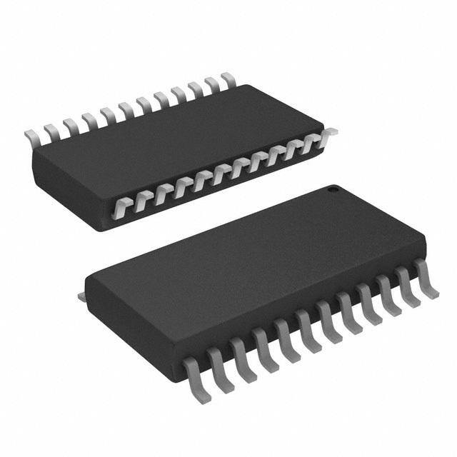
| 描述 | IC TXRX DUAL RS232 5V 24-SOIC |
| 产品分类 | |
| 品牌 | Texas Instruments |
| 数据手册 | |
| 产品图片 |
|
| 产品型号 | MAX207CDWR |
| rohs | 无铅 / 符合限制有害物质指令(RoHS)规范要求 |
| 产品系列 | - |
| 供应商器件封装 | 24-SOIC |
| 其它名称 | 296-18487-1 |
| 包装 | 剪切带 (CT) |
| 协议 | RS232 |
| 双工 | 全 |
| 安装类型 | 表面贴装 |
| 封装/外壳 | 24-SOIC(0.295",7.50mm 宽) |
| 工作温度 | 0°C ~ 70°C |
| 接收器滞后 | 500mV |
| 数据速率 | 120Kbps |
| 标准包装 | 1 |
| 电压-电源 | 4.75 V ~ 5.25 V |
| 类型 | 收发器 |
| 驱动器/接收器数 | 5/3 |


- 商务部:美国ITC正式对集成电路等产品启动337调查
- 曝三星4nm工艺存在良率问题 高通将骁龙8 Gen1或转产台积电
- 太阳诱电将投资9.5亿元在常州建新厂生产MLCC 预计2023年完工
- 英特尔发布欧洲新工厂建设计划 深化IDM 2.0 战略
- 台积电先进制程称霸业界 有大客户加持明年业绩稳了
- 达到5530亿美元!SIA预计今年全球半导体销售额将创下新高
- 英特尔拟将自动驾驶子公司Mobileye上市 估值或超500亿美元
- 三星加码芯片和SET,合并消费电子和移动部门,撤换高东真等 CEO
- 三星电子宣布重大人事变动 还合并消费电子和移动部门
- 海关总署:前11个月进口集成电路产品价值2.52万亿元 增长14.8%


.jpg)

PDF Datasheet 数据手册内容提取
(cid:1)(cid:2)(cid:3)(cid:4)(cid:5)(cid:6) (cid:7)(cid:8)(cid:9) (cid:1)(cid:10)(cid:11)(cid:12)(cid:13)(cid:14)(cid:15)(cid:2)(cid:16)(cid:16)(cid:17)(cid:11) (cid:18)(cid:19)(cid:8)(cid:4)(cid:20)(cid:4) (cid:11)(cid:13)(cid:16)(cid:17) (cid:21)(cid:18)(cid:13)(cid:9)(cid:17)(cid:18)(cid:22)(cid:18)(cid:17)(cid:14)(cid:17)(cid:13)(cid:9)(cid:17)(cid:18) (cid:23)(cid:13)(cid:12)(cid:15) ±(cid:24)(cid:7)(cid:8)(cid:25)(cid:9) (cid:17)(cid:19)(cid:21) (cid:26)(cid:18)(cid:27)(cid:12)(cid:17)(cid:14)(cid:12)(cid:13)(cid:27)(cid:16) SLLS592B − OCTOBER 2003 − REVISED JANUARY 2004 (cid:1) ESD Protection for RS-232 I/O Pins DB OR DW PACKAGE − ±15 kV − Human-Body Model (TOP VIEW) (cid:1) Meets or Exceeds the Requirements of DOUT3 1 24 DOUT4 TIA/EIA-232-F and ITU v.28 Standards DOUT1 2 23 RIN2 (cid:1) Operates at 5-V VCC Supply DOUT2 3 22 ROUT2 (cid:1) Operates Up To 120 kbit/s RIN1 4 21 DIN5 (cid:1) External Capacitors...4 × 0.1 µF ROUT1 5 20 DOUT5 (cid:1) DIN2 6 19 DIN4 Latch-Up Performance Exceeds 100 mA Per DIN1 7 18 DIN3 JESD 78, Class II GND 8 17 ROUT3 (cid:1) Applications VCC 9 16 RIN3 − Battery-Powered Systems, PDAs, C1+ 10 15 V− Notebooks, Laptops, Palmtop PCs, and V+ 11 14 C2− Hand-Held Equipment C1− 12 13 C2+ description/ordering information The MAX207 consists of five line drivers, three line receivers, and a dual charge-pump circuit with ±15-kV ESD protection pin to pin (serial-port connection pins, including GND). The device meets the requirements of TIA/EIA-232-F and provides the electrical interface between an asynchronous communication controller and the serial-port connector. The charge pump and four small external capacitors allow operation from a single 5-V supply. The devices operate at data signaling rates up to 120 kbit/s and a maximum of 30-V/µs driver output slew rate. ORDERING INFORMATION ORDERABLE TOP-SIDE TA PACKAGE† PART NUMBER MARKING Tube of 25 MAX207CDW SSOOIICC ((DDWW)) MMAAXX220077CC 00°CC ttoo 7700°CC Reel of 2000 MAX207CDWR SSOP (DB) Reel of 2000 MAX207CDBR MA207C Tube of 25 MAX207IDW SSOOIICC ((DDWW)) MMAAXX220077II −−4400°CC ttoo 8855°CC Reel of 2000 MAX207IDWR SSOP (DB) Reel of 2000 MAX207IDBR MB207I †Package drawings, standard packing quantities, thermal data, symbolization, and PCB design guidelines are available at www.ti.com/sc/package. Please be aware that an important notice concerning availability, standard warranty, and use in critical applications of TexasInstruments semiconductor products and disclaimers thereto appears at the end of this data sheet. (cid:26)(cid:18)(cid:27)(cid:21)(cid:10)(cid:14)(cid:12)(cid:13)(cid:27)(cid:16) (cid:21)(cid:2)(cid:12)(cid:2) (cid:28)(cid:29)(cid:30)(cid:31)!"#$(cid:28)(cid:31)(cid:29) (cid:28)% &’!!((cid:29)$ #% (cid:31)(cid:30) )’*+(cid:28)&#$(cid:28)(cid:31)(cid:29) ,#$(- Copyright 2004, Texas Instruments Incorporated (cid:26)!(cid:31),’&$% &(cid:31)(cid:29)(cid:30)(cid:31)!" $(cid:31) %)(&(cid:28)(cid:30)(cid:28)&#$(cid:28)(cid:31)(cid:29)% )(! $.( $(!"% (cid:31)(cid:30) (cid:12)(/#% (cid:13)(cid:29)%$!’"((cid:29)$% %$#(cid:29),#!, 0#!!#(cid:29)$1- (cid:26)!(cid:31),’&$(cid:28)(cid:31)(cid:29) )!(cid:31)&(%%(cid:28)(cid:29)2 ,(cid:31)(% (cid:29)(cid:31)$ (cid:29)(&(%%#!(cid:28)+1 (cid:28)(cid:29)&+’,( $(%$(cid:28)(cid:29)2 (cid:31)(cid:30) #++ )#!#"($(!%- POST OFFICE BOX 655303 • DALLAS, TEXAS 75265 1
(cid:1)(cid:2)(cid:3)(cid:4)(cid:5)(cid:6) (cid:7)(cid:8)(cid:9) (cid:1)(cid:10)(cid:11)(cid:12)(cid:13)(cid:14)(cid:15)(cid:2)(cid:16)(cid:16)(cid:17)(cid:11) (cid:18)(cid:19)(cid:8)(cid:4)(cid:20)(cid:4) (cid:11)(cid:13)(cid:16)(cid:17) (cid:21)(cid:18)(cid:13)(cid:9)(cid:17)(cid:18)(cid:22)(cid:18)(cid:17)(cid:14)(cid:17)(cid:13)(cid:9)(cid:17)(cid:18) (cid:23)(cid:13)(cid:12)(cid:15) ±(cid:24)(cid:7)(cid:8)(cid:25)(cid:9) (cid:17)(cid:19)(cid:21) (cid:26)(cid:18)(cid:27)(cid:12)(cid:17)(cid:14)(cid:12)(cid:13)(cid:27)(cid:16) SLLS592B − OCTOBER 2003 − REVISED JANUARY 2004 Function Tables EACH DRIVER INPUT OUTPUT DIN DOUT L H H L H = high level, L = low level EACH RECEIVER INPUT OUTPUT RIN ROUT L H H L Open H H = high level, L = low level, Open = input disconnected or connected driver off logic diagram (positive logic) 7 2 DIN1 DOUT1 6 3 DIN2 DOUT2 TTL/CMOS 18 1 RS-232 DIN3 DOUT3 Inputs Outputs 19 24 DIN4 DOUT4 21 20 DIN5 DOUT5 5 4 ROUT1 RIN1 TTL/CMOS 22 23 RS-232 ROUT2 RIN2 Outputs Inputs 17 16 ROUT3 RIN3 2 POST OFFICE BOX 655303 • DALLAS, TEXAS 75265
(cid:1)(cid:2)(cid:3)(cid:4)(cid:5)(cid:6) (cid:7)(cid:8)(cid:9) (cid:1)(cid:10)(cid:11)(cid:12)(cid:13)(cid:14)(cid:15)(cid:2)(cid:16)(cid:16)(cid:17)(cid:11) (cid:18)(cid:19)(cid:8)(cid:4)(cid:20)(cid:4) (cid:11)(cid:13)(cid:16)(cid:17) (cid:21)(cid:18)(cid:13)(cid:9)(cid:17)(cid:18)(cid:22)(cid:18)(cid:17)(cid:14)(cid:17)(cid:13)(cid:9)(cid:17)(cid:18) (cid:23)(cid:13)(cid:12)(cid:15) ±(cid:24)(cid:7)(cid:8)(cid:25)(cid:9) (cid:17)(cid:19)(cid:21) (cid:26)(cid:18)(cid:27)(cid:12)(cid:17)(cid:14)(cid:12)(cid:13)(cid:27)(cid:16) SLLS592B − OCTOBER 2003 − REVISED JANUARY 2004 absolute maximum ratings over operating free-air temperature range (unless otherwise noted)† Supply voltage range, V (see Note 1) . . . . . . . . . . . . . . . . . . . . . . . . . . . . . . . . . . . . . . . . . . . . . . −0.3 V to 6 V CC Positive charge pump voltage range, V+ (see Note 1) . . . . . . . . . . . . . . . . . . . . . . . . . . . . VCC − 0.3 V to 14 V Negative charge pump voltage range, V− (see Note 1) . . . . . . . . . . . . . . . . . . . . . . . . . . . . . . . . . −14 V to 0.3 V Input voltage range, V: Drivers . . . . . . . . . . . . . . . . . . . . . . . . . . . . . . . . . . . . . . . . . . . . . . . . −0.3 V to V+ + 0.3 V I Receivers . . . . . . . . . . . . . . . . . . . . . . . . . . . . . . . . . . . . . . . . . . . . . . . . . . . . . . . . . . ±30 V Output voltage range, VO: Drivers . . . . . . . . . . . . . . . . . . . . . . . . . . . . . . . . . . . . . . . . . V− − 0.3 V to V+ + 0.3 V Receivers . . . . . . . . . . . . . . . . . . . . . . . . . . . . . . . . . . . . . . . . . . −0.3 V to V + 0.3 V CC Short-circuit duration: D . . . . . . . . . . . . . . . . . . . . . . . . . . . . . . . . . . . . . . . . . . . . . . . . . . . . . . . . . . Continuous OUT Package thermal impedance, θ (see Notes 2 and 3): DB package . . . . . . . . . . . . . . . . . . . . . . . . . . . 63°C/W JA DW package . . . . . . . . . . . . . . . . . . . . . . . . . . 46°C/W Operating virtual junction temperature, T . . . . . . . . . . . . . . . . . . . . . . . . . . . . . . . . . . . . . . . . . . . . . . . . . . . 150°C J Storage temperature range, T . . . . . . . . . . . . . . . . . . . . . . . . . . . . . . . . . . . . . . . . . . . . . . . . . . . −65°C to 150°C stg †Stresses beyond those listed under “absolute maximum ratings” may cause permanent damage to the device. These are stress ratings only, and functional operation of the device at these or any other conditions beyond those indicated under “recommended operating conditions” is not implied. Exposure to absolute-maximum-rated conditions for extended periods may affect device reliability. NOTES: 1. All voltages are with respect to network GND. θ 2. Maximum power dissipation is a function of TJ(max), JA, and TA. The maximum allowable power dissipation at any allowable ambient temperature is PD = (TJ(max) − TA)/θJA. Operating at the absolute maximum TJ of 150°C can affect reliability. 3. The package thermal impedance is calculated in accordance with JESD 51-7. recommended operating conditions (see Note 4 and Figure 4) MIN NOM MAX UNIT Supply voltage 4.5 5 5.5 V VIH Driver high-level input voltage DIN 2 V VIL Driver low-level input voltage DIN 0.8 V Driver input voltage DIN 0 5.5 VVII VV Receiver input voltage −30 30 MAX207C 0 70 TTAA OOppeerraattiinngg ffrreeee--aaiirr tteemmppeerraattuurree °°CC MAX207I −40 85 NOTE 4: Test conditions are C1−C4 = 0.1 µF at VCC = 5 V ±0.5 V. electrical characteristics over recommended ranges of supply voltage (unless otherwise noted) (see Note 4 and Figure 4) PARAMETER TEST CONDITIONS MIN TYP MAX UNIT ICC Supply current No load, VCC = 5 V, TA = 25°C 11 20 mA NOTE 4: Test conditions are C1−C4 = 0.1 µF at VCC = 5 V ±0.5 V. POST OFFICE BOX 655303 • DALLAS, TEXAS 75265 3
(cid:1)(cid:2)(cid:3)(cid:4)(cid:5)(cid:6) (cid:7)(cid:8)(cid:9) (cid:1)(cid:10)(cid:11)(cid:12)(cid:13)(cid:14)(cid:15)(cid:2)(cid:16)(cid:16)(cid:17)(cid:11) (cid:18)(cid:19)(cid:8)(cid:4)(cid:20)(cid:4) (cid:11)(cid:13)(cid:16)(cid:17) (cid:21)(cid:18)(cid:13)(cid:9)(cid:17)(cid:18)(cid:22)(cid:18)(cid:17)(cid:14)(cid:17)(cid:13)(cid:9)(cid:17)(cid:18) (cid:23)(cid:13)(cid:12)(cid:15) ±(cid:24)(cid:7)(cid:8)(cid:25)(cid:9) (cid:17)(cid:19)(cid:21) (cid:26)(cid:18)(cid:27)(cid:12)(cid:17)(cid:14)(cid:12)(cid:13)(cid:27)(cid:16) SLLS592B − OCTOBER 2003 − REVISED JANUARY 2004 DRIVER SECTION electrical characteristics over recommended ranges of supply voltage and operating free-air temperature (unless otherwise noted) (see Note 4 and Figure 4) PARAMETER TEST CONDITIONS MIN TYP† MAX UNIT VOH High-level output voltage DOUT at RL = 3 kΩ to GND, DIN = GND 5 9 V VOL Low-level output voltage DOUT at RL = 3 kΩ to GND, DIN = VCC −5 −9 V IIH High-level input current VI = VCC 15 200 µA IIL Low-level input current VI at 0 V −15 −200 µA IOS‡ Short-circuit output current VCC = 5.5 V, VO = 0 V ±10 ±60 mA ro Output resistance VCC, V+, and V− = 0 V, VO = ±2 V 300 (cid:1) †All typical values are at VCC = 5 V, and TA = 25°C. ‡Short-circuit durations should be controlled to prevent exceeding the device absolute power-dissipation ratings, and not more than one output should be shorted at a time. NOTE 4: Test conditions are C1−C4 = 0.1 µF at VCC = 5 V ±0.5 V. switching characteristics over recommended ranges of supply voltage and operating free-air temperature (unless otherwise noted) (see Note 4 and Figure 4) PARAMETER TEST CONDITIONS MIN TYP† MAX UNIT CL = 50 to 1000 pF, RL = 3 kΩ to 7 kΩ, Maximum data rate 120 kbit/s One DOUT switching, See Figure 1 tPLH (D) Plorwo-p taog haitgiohn- ledveelal yo utimtpeu,t CalLl d =r iv2e5r0s0 l opaFd,ed, RSeLe = F 3ig kuΩre, 1 2 µs tPHL (D) Phirgohp-a tgoa ltoiown- ledveelal yo utimtpeu,t CalLl d =r iv2e5r0s0 l opaFd,ed, RSeLe = F 3ig kuΩre, 1 2 µs tsk(p) Pulse skew§ CL = 150 pF to 2500 pF, RSeLe = F 3ig kuΩre t o2 7 kΩ, 300 ns SR(tr) Slew rate, transition region CL = 50 pF to 1000 pF RL = 3 kΩ to 7 kΩ, 3 6 30 V/µs (see Figure 1) VCC = 5 V †All typical values are at VCC = 5 V, and TA = 25°C. §Pulse skew is defined as |tPLH − tPHL| of each channel of the same device. NOTE 4: Test conditions are C1−C4 = 0.1 µF at VCC = 5 V ±0.5 V. ESD protection PIN TEST CONDITIONS TYP UNIT DOUT, RIN Human-Body Model ±15 kV 4 POST OFFICE BOX 655303 • DALLAS, TEXAS 75265
(cid:1)(cid:2)(cid:3)(cid:4)(cid:5)(cid:6) (cid:7)(cid:8)(cid:9) (cid:1)(cid:10)(cid:11)(cid:12)(cid:13)(cid:14)(cid:15)(cid:2)(cid:16)(cid:16)(cid:17)(cid:11) (cid:18)(cid:19)(cid:8)(cid:4)(cid:20)(cid:4) (cid:11)(cid:13)(cid:16)(cid:17) (cid:21)(cid:18)(cid:13)(cid:9)(cid:17)(cid:18)(cid:22)(cid:18)(cid:17)(cid:14)(cid:17)(cid:13)(cid:9)(cid:17)(cid:18) (cid:23)(cid:13)(cid:12)(cid:15) ±(cid:24)(cid:7)(cid:8)(cid:25)(cid:9) (cid:17)(cid:19)(cid:21) (cid:26)(cid:18)(cid:27)(cid:12)(cid:17)(cid:14)(cid:12)(cid:13)(cid:27)(cid:16) SLLS592B − OCTOBER 2003 − REVISED JANUARY 2004 RECEIVER SECTION electrical characteristics over recommended ranges of supply voltage and operating free-air temperature (unless otherwise noted) (see Note 4 and Figure 4) PARAMETER TEST CONDITIONS MIN TYP† MAX UNIT VOH High-level output voltage IOH = −1 mA 3.5 VCC−0.4 V V VOL Low-level output voltage IOL = 1.6 mA 0.4 V VIT+ Positive-going input threshold voltage VCC = 5 V, TA = 25°C 1.7 2.4 V VIT− Negative-going input threshold voltage VCC = 5 V, TA = 25°C 0.8 1.2 V Vhys Input hysteresis (VIT+ − VIT−) 0.2 0.5 1 V ri Input resistance VI = ±3 V to ±25 V 3 5 7 k(cid:1) †All typical values are at VCC = 5 V, and TA = 25°C. NOTE 4: Test conditions are C1−C4 = 0.1 µF at VCC = 5 V ±0.5 V. switching characteristics over recommended ranges of supply voltage and operating free-air temperature (unless otherwise noted) (see Note 4 and Figure 3) PARAMETER TEST CONDITIONS MIN TYP† MAX UNIT tPLH Propagation delay time, low- to high-level output 0.5 10 µs tPHL Propagation delay time, high- to low-level output CCLL== 115500 ppFF 0.5 10 µs tsk(p) Pulse skew‡ 300 ns †All typical values are at VCC = 5 V, and TA = 25°C. ‡Pulse skew is defined as |tPLH − tPHL| of each channel of the same device. NOTE 4: Test conditions are C1−C4 = 0.1 µF, at VCC = 5 V ±0.5 V. PARAMETER MEASUREMENT INFORMATION 3 V Input 1.5 V 1.5 V RS-232 0 V Output Generator (see Note B) 50 Ω CL tPHL (D) tPLH (D) RL (see Note A) VOH 3 V 3 V Output −3 V −3 V VOL TEST CIRCUIT SR(tr)(cid:1) 6V VOLTAGE WAVEFORMS t ort PHL(D) PLH(D) NOTES: A. CL includes probe and jig capacitance. B. The pulse generator has the following characteristics: PRR = 120 kbit/s, ZO = 50 Ω, 50% duty cycle, tr ≤10 ns, tf ≤ 10 ns. Figure 1. Driver Slew Rate POST OFFICE BOX 655303 • DALLAS, TEXAS 75265 5
(cid:1)(cid:2)(cid:3)(cid:4)(cid:5)(cid:6) (cid:7)(cid:8)(cid:9) (cid:1)(cid:10)(cid:11)(cid:12)(cid:13)(cid:14)(cid:15)(cid:2)(cid:16)(cid:16)(cid:17)(cid:11) (cid:18)(cid:19)(cid:8)(cid:4)(cid:20)(cid:4) (cid:11)(cid:13)(cid:16)(cid:17) (cid:21)(cid:18)(cid:13)(cid:9)(cid:17)(cid:18)(cid:22)(cid:18)(cid:17)(cid:14)(cid:17)(cid:13)(cid:9)(cid:17)(cid:18) (cid:23)(cid:13)(cid:12)(cid:15) ±(cid:24)(cid:7)(cid:8)(cid:25)(cid:9) (cid:17)(cid:19)(cid:21) (cid:26)(cid:18)(cid:27)(cid:12)(cid:17)(cid:14)(cid:12)(cid:13)(cid:27)(cid:16) SLLS592B − OCTOBER 2003 − REVISED JANUARY 2004 PARAMETER MEASUREMENT INFORMATION 3 V RS-232 Input 1.5 V 1.5 V Generator Output 0 V (see Note B) 50 Ω CL tPHL (D) tPLH (D) RL (see Note A) VOH Output 50% 50% VOL TEST CIRCUIT VOLTAGE WAVEFORMS NOTES: A. CL includes probe and jig capacitance. B. The pulse generator has the following characteristics: PRR = 120 kbit/s, ZO = 50 Ω, 50% duty cycle, tr ≤ 10 ns, tf ≤ 10 ns. Figure 2. Driver Pulse Skew 3 V Input 1.5 V 1.5 V Output −3 V Generator (see Note B) 50 Ω CL tPHL (R) tPLH (R) (see Note A) VOH Output 50% 50% VOL TEST CIRCUIT VOLTAGE WAVEFORMS NOTES: A. CL includes probe and jig capacitance. B. The pulse generator has the following characteristics: ZO = 50 Ω, 50% duty cycle, tr ≤ 10 ns, tf ≤ 10 ns. Figure 3. Receiver Propagation Delay Times 6 POST OFFICE BOX 655303 • DALLAS, TEXAS 75265
(cid:1)(cid:2)(cid:3)(cid:4)(cid:5)(cid:6) (cid:7)(cid:8)(cid:9) (cid:1)(cid:10)(cid:11)(cid:12)(cid:13)(cid:14)(cid:15)(cid:2)(cid:16)(cid:16)(cid:17)(cid:11) (cid:18)(cid:19)(cid:8)(cid:4)(cid:20)(cid:4) (cid:11)(cid:13)(cid:16)(cid:17) (cid:21)(cid:18)(cid:13)(cid:9)(cid:17)(cid:18)(cid:22)(cid:18)(cid:17)(cid:14)(cid:17)(cid:13)(cid:9)(cid:17)(cid:18) (cid:23)(cid:13)(cid:12)(cid:15) ±(cid:24)(cid:7)(cid:8)(cid:25)(cid:9) (cid:17)(cid:19)(cid:21) (cid:26)(cid:18)(cid:27)(cid:12)(cid:17)(cid:14)(cid:12)(cid:13)(cid:27)(cid:16) SLLS592B − OCTOBER 2003 − REVISED JANUARY 2004 APPLICATION INFORMATION 1 24 DOUT3 DOUT4 2 23 DOUT1 RIN2 5 kΩ 3 22 DOUT2 ROUT2 4 RIN1 5 V 5 kΩ 400 kΩ 21 DIN5 5 ROUT1 20 DOUT5 5 V 5 V 400 kΩ 6 400 kΩ DIN2 19 DIN4 5 V 5 V 400 kΩ 400 kΩ 7 18 DIN1 DIN3 GND 8 17 ROUT3 + CBYPASS 16 − = 0.1µF RIN3 5 kΩ C4 = 9 0.1 µF VCC 15 16 V C3†= − V− − + 0.1 µF + 10 6.3 V C1+ 14 C2− 11 V+ − C2 = + 0.1 µF + C1 = 16 V 0.1 µF − 12 C1− C2+ 13 6.3 V †C3 can be connected to VCC or GND. NOTES: A. Resistor values shown are nominal. B. Nonpolarized ceramic capacitors are acceptable. If polarized tantalum or electrolytic capacitors are used, they should be connected as shown. Figure 4. Typical Operating Circuit and Capacitor Values POST OFFICE BOX 655303 • DALLAS, TEXAS 75265 7
(cid:1)(cid:2)(cid:3)(cid:4)(cid:5)(cid:6) (cid:7)(cid:8)(cid:9) (cid:1)(cid:10)(cid:11)(cid:12)(cid:13)(cid:14)(cid:15)(cid:2)(cid:16)(cid:16)(cid:17)(cid:11) (cid:18)(cid:19)(cid:8)(cid:4)(cid:20)(cid:4) (cid:11)(cid:13)(cid:16)(cid:17) (cid:21)(cid:18)(cid:13)(cid:9)(cid:17)(cid:18)(cid:22)(cid:18)(cid:17)(cid:14)(cid:17)(cid:13)(cid:9)(cid:17)(cid:18) (cid:23)(cid:13)(cid:12)(cid:15) ±(cid:24)(cid:7)(cid:8)(cid:25)(cid:9) (cid:17)(cid:19)(cid:21) (cid:26)(cid:18)(cid:27)(cid:12)(cid:17)(cid:14)(cid:12)(cid:13)(cid:27)(cid:16) SLLS592B − OCTOBER 2003 − REVISED JANUARY 2004 APPLICATION INFORMATION capacitor selection The capacitor type used for C1−C4 is not critical for proper operation. The MAX207 requires 0.1-µF capacitors, although capacitors up to 10 µF can be used without harm. Ceramic dielectrics are suggested for the 0.1-µF capacitors. When using the minimum recommended capacitor values, make sure the capacitance value does not degrade excessively as the operating temperature varies. If in doubt, use capacitors with a larger (e.g., 2×) nominal value. The capacitors’ effective series resistance (ESR), which usually rises at low temperatures, influences the amount of ripple on V+ and V−. Use larger capacitors (up to 10 µF) to reduce the output impedance at V+ and V−. Bypass V to ground with at least 0.1 µF. In applications sensitive to power-supply noise generated by the CC charge pumps, decouple V to ground with a capacitor the same size as (or larger than) the charge-pump CC capacitors (C1−C4). ESD protection TI MAX207 devices have standard ESD protection structures incorporated on the pins to protect against electrostatic discharges encountered during assembly and handling. In addition, the RS232 bus pins (driver outputs and receiver inputs) of these devices have an extra level of ESD protection. Advanced ESD structures were designed to successfully protect these bus pins against ESD discharge of ±15-kV when powered down. ESD test conditions ESD testing is stringently performed by TI, based on various conditions and procedures. Please contact TI for a reliability report that documents test setup, methodology, and results. Human-Body Model The Human-Body Model (HBM) of ESD testing is shown in Figure 5, while Figure 6 shows the current waveform that is generated during a discharge into a low impedance. The model consists of a 100-pF capacitor, charged to the ESD voltage of concern, and subsequently discharged into the device under test (DUT) through a 1.5-kΩ resistor. RD 1.5 kΩ + CS VHBM − 100 pF DUT Figure 5. HBM ESD Test Circuit 8 POST OFFICE BOX 655303 • DALLAS, TEXAS 75265
(cid:1)(cid:2)(cid:3)(cid:4)(cid:5)(cid:6) (cid:7)(cid:8)(cid:9) (cid:1)(cid:10)(cid:11)(cid:12)(cid:13)(cid:14)(cid:15)(cid:2)(cid:16)(cid:16)(cid:17)(cid:11) (cid:18)(cid:19)(cid:8)(cid:4)(cid:20)(cid:4) (cid:11)(cid:13)(cid:16)(cid:17) (cid:21)(cid:18)(cid:13)(cid:9)(cid:17)(cid:18)(cid:22)(cid:18)(cid:17)(cid:14)(cid:17)(cid:13)(cid:9)(cid:17)(cid:18) (cid:23)(cid:13)(cid:12)(cid:15) ±(cid:24)(cid:7)(cid:8)(cid:25)(cid:9) (cid:17)(cid:19)(cid:21) (cid:26)(cid:18)(cid:27)(cid:12)(cid:17)(cid:14)(cid:12)(cid:13)(cid:27)(cid:16) SLLS592B − OCTOBER 2003 − REVISED JANUARY 2004 APPLICATION INFORMATION 1.5 VHBM = 2 kV DUT = 10-V, 1-Ω Zener Diode 1.0 A − T U D I 0.5 0.0 0 50 100 150 200 Time − ns Figure 6. Typical HBM Current Waveform Machine Model The Machine Model (MM) ESD test applies to all pins using a 200-pF capacitor with no discharge resistance. The purpose of the MM test is to simulate possible ESD conditions that can occur during the handling and assembly processes of manufacturing. In this case, ESD protection is required for all pins, not just RS-232 pins. However, after PC board assembly, the MM test no longer is as pertinent to the RS-232 pins. POST OFFICE BOX 655303 • DALLAS, TEXAS 75265 9
PACKAGE OPTION ADDENDUM www.ti.com 6-Feb-2020 PACKAGING INFORMATION Orderable Device Status Package Type Package Pins Package Eco Plan Lead/Ball Finish MSL Peak Temp Op Temp (°C) Device Marking Samples (1) Drawing Qty (2) (6) (3) (4/5) MAX207CDB ACTIVE SSOP DB 24 60 Green (RoHS NIPDAU Level-1-260C-UNLIM 0 to 70 MA207C & no Sb/Br) MAX207CDBR ACTIVE SSOP DB 24 2000 Green (RoHS NIPDAU Level-1-260C-UNLIM 0 to 70 MA207C & no Sb/Br) MAX207CDW ACTIVE SOIC DW 24 25 Green (RoHS NIPDAU Level-1-260C-UNLIM 0 to 70 MAX207C & no Sb/Br) MAX207CDWR ACTIVE SOIC DW 24 2000 Green (RoHS NIPDAU Level-1-260C-UNLIM 0 to 70 MAX207C & no Sb/Br) MAX207IDB ACTIVE SSOP DB 24 60 Green (RoHS NIPDAU Level-1-260C-UNLIM -40 to 85 MB207I & no Sb/Br) MAX207IDBR ACTIVE SSOP DB 24 2000 Green (RoHS NIPDAU Level-1-260C-UNLIM -40 to 85 MB207I & no Sb/Br) MAX207IDW ACTIVE SOIC DW 24 25 Green (RoHS NIPDAU Level-1-260C-UNLIM -40 to 85 MAX207I & no Sb/Br) MAX207IDWR ACTIVE SOIC DW 24 2000 Green (RoHS NIPDAU Level-1-260C-UNLIM -40 to 85 MAX207I & no Sb/Br) (1) The marketing status values are defined as follows: ACTIVE: Product device recommended for new designs. LIFEBUY: TI has announced that the device will be discontinued, and a lifetime-buy period is in effect. NRND: Not recommended for new designs. Device is in production to support existing customers, but TI does not recommend using this part in a new design. PREVIEW: Device has been announced but is not in production. Samples may or may not be available. OBSOLETE: TI has discontinued the production of the device. (2) RoHS: TI defines "RoHS" to mean semiconductor products that are compliant with the current EU RoHS requirements for all 10 RoHS substances, including the requirement that RoHS substance do not exceed 0.1% by weight in homogeneous materials. Where designed to be soldered at high temperatures, "RoHS" products are suitable for use in specified lead-free processes. TI may reference these types of products as "Pb-Free". RoHS Exempt: TI defines "RoHS Exempt" to mean products that contain lead but are compliant with EU RoHS pursuant to a specific EU RoHS exemption. Green: TI defines "Green" to mean the content of Chlorine (Cl) and Bromine (Br) based flame retardants meet JS709B low halogen requirements of <=1000ppm threshold. Antimony trioxide based flame retardants must also meet the <=1000ppm threshold requirement. (3) MSL, Peak Temp. - The Moisture Sensitivity Level rating according to the JEDEC industry standard classifications, and peak solder temperature. (4) There may be additional marking, which relates to the logo, the lot trace code information, or the environmental category on the device. Addendum-Page 1
PACKAGE OPTION ADDENDUM www.ti.com 6-Feb-2020 (5) Multiple Device Markings will be inside parentheses. Only one Device Marking contained in parentheses and separated by a "~" will appear on a device. If a line is indented then it is a continuation of the previous line and the two combined represent the entire Device Marking for that device. (6) Lead/Ball Finish - Orderable Devices may have multiple material finish options. Finish options are separated by a vertical ruled line. Lead/Ball Finish values may wrap to two lines if the finish value exceeds the maximum column width. Important Information and Disclaimer:The information provided on this page represents TI's knowledge and belief as of the date that it is provided. TI bases its knowledge and belief on information provided by third parties, and makes no representation or warranty as to the accuracy of such information. Efforts are underway to better integrate information from third parties. TI has taken and continues to take reasonable steps to provide representative and accurate information but may not have conducted destructive testing or chemical analysis on incoming materials and chemicals. TI and TI suppliers consider certain information to be proprietary, and thus CAS numbers and other limited information may not be available for release. In no event shall TI's liability arising out of such information exceed the total purchase price of the TI part(s) at issue in this document sold by TI to Customer on an annual basis. Addendum-Page 2
PACKAGE MATERIALS INFORMATION www.ti.com 14-Feb-2019 TAPE AND REEL INFORMATION *Alldimensionsarenominal Device Package Package Pins SPQ Reel Reel A0 B0 K0 P1 W Pin1 Type Drawing Diameter Width (mm) (mm) (mm) (mm) (mm) Quadrant (mm) W1(mm) MAX207CDBR SSOP DB 24 2000 330.0 16.4 8.2 8.8 2.5 12.0 16.0 Q1 MAX207CDWR SOIC DW 24 2000 330.0 24.4 10.75 15.7 2.7 12.0 24.0 Q1 MAX207IDBR SSOP DB 24 2000 330.0 16.4 8.2 8.8 2.5 12.0 16.0 Q1 MAX207IDWR SOIC DW 24 2000 330.0 24.4 10.75 15.7 2.7 12.0 24.0 Q1 PackMaterials-Page1
PACKAGE MATERIALS INFORMATION www.ti.com 14-Feb-2019 *Alldimensionsarenominal Device PackageType PackageDrawing Pins SPQ Length(mm) Width(mm) Height(mm) MAX207CDBR SSOP DB 24 2000 367.0 367.0 38.0 MAX207CDWR SOIC DW 24 2000 350.0 350.0 43.0 MAX207IDBR SSOP DB 24 2000 367.0 367.0 38.0 MAX207IDWR SOIC DW 24 2000 350.0 350.0 43.0 PackMaterials-Page2
None
MECHANICAL DATA MSSO002E – JANUARY 1995 – REVISED DECEMBER 2001 DB (R-PDSO-G**) PLASTIC SMALL-OUTLINE 28 PINS SHOWN 0,38 0,65 0,15 M 0,22 28 15 0,25 0,09 5,60 8,20 5,00 7,40 Gage Plane 1 14 0,25 A 0°–(cid:1)8° 0,95 0,55 Seating Plane 2,00 MAX 0,05 MIN 0,10 PINS ** 14 16 20 24 28 30 38 DIM A MAX 6,50 6,50 7,50 8,50 10,50 10,50 12,90 A MIN 5,90 5,90 6,90 7,90 9,90 9,90 12,30 4040065/E 12/01 NOTES: A. All linear dimensions are in millimeters. B. This drawing is subject to change without notice. C. Body dimensions do not include mold flash or protrusion not to exceed 0,15. D. Falls within JEDEC MO-150 • POST OFFICE BOX 655303 DALLAS, TEXAS 75265
IMPORTANTNOTICEANDDISCLAIMER TI PROVIDES TECHNICAL AND RELIABILITY DATA (INCLUDING DATASHEETS), DESIGN RESOURCES (INCLUDING REFERENCE DESIGNS), APPLICATION OR OTHER DESIGN ADVICE, WEB TOOLS, SAFETY INFORMATION, AND OTHER RESOURCES “AS IS” AND WITH ALL FAULTS, AND DISCLAIMS ALL WARRANTIES, EXPRESS AND IMPLIED, INCLUDING WITHOUT LIMITATION ANY IMPLIED WARRANTIES OF MERCHANTABILITY, FITNESS FOR A PARTICULAR PURPOSE OR NON-INFRINGEMENT OF THIRD PARTY INTELLECTUAL PROPERTY RIGHTS. These resources are intended for skilled developers designing with TI products. You are solely responsible for (1) selecting the appropriate TI products for your application, (2) designing, validating and testing your application, and (3) ensuring your application meets applicable standards, and any other safety, security, or other requirements. These resources are subject to change without notice. TI grants you permission to use these resources only for development of an application that uses the TI products described in the resource. Other reproduction and display of these resources is prohibited. No license is granted to any other TI intellectual property right or to any third party intellectual property right. TI disclaims responsibility for, and you will fully indemnify TI and its representatives against, any claims, damages, costs, losses, and liabilities arising out of your use of these resources. TI’s products are provided subject to TI’s Terms of Sale (www.ti.com/legal/termsofsale.html) or other applicable terms available either on ti.com or provided in conjunction with such TI products. TI’s provision of these resources does not expand or otherwise alter TI’s applicable warranties or warranty disclaimers for TI products. Mailing Address: Texas Instruments, Post Office Box 655303, Dallas, Texas 75265 Copyright © 2020, Texas Instruments Incorporated