ICGOO在线商城 > 射频/IF 和 RFID > RF 开关 > MASW-004100-11930W

 Datasheet下载
- 型号: MASW-004100-11930W
- 制造商: M/A-COM
- 库位|库存: xxxx|xxxx
- 要求:
| 数量阶梯 | 香港交货 | 国内含税 |
| +xxxx | $xxxx | ¥xxxx |
查看当月历史价格
查看今年历史价格
MASW-004100-11930W产品简介:
ICGOO电子元器件商城为您提供MASW-004100-11930W由M/A-COM设计生产,在icgoo商城现货销售,并且可以通过原厂、代理商等渠道进行代购。 MASW-004100-11930W价格参考。M/A-COMMASW-004100-11930W封装/规格:RF 开关, 射频开关 IC 通用 SP4T 26GHz 。您可以下载MASW-004100-11930W参考资料、Datasheet数据手册功能说明书,资料中有MASW-004100-11930W 详细功能的应用电路图电压和使用方法及教程。
| 参数 | 数值 |
| 产品目录 | |
| 描述 | DIODE CHIP HMIC SP4T 2WATTRF 开关 IC 50-26000MHz -65C +125C Iso 65dB |
| 产品分类 | |
| IIP3 | - |
| 品牌 | MACOMM/A-Com Technology Solutions |
| 产品手册 | |
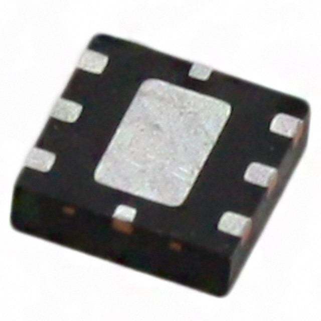
| 产品图片 |
|
| rohs | 符合RoHS无铅 / 符合限制有害物质指令(RoHS)规范要求 |
| 产品系列 | RF集成电路,RF 开关 IC,MACOM MASW-004100-11930WHMIC™ |
| 数据手册 | |
| P1dB | - |
| 产品型号 | MASW-004100-11930WMASW-004100-11930W |
| RF类型 | 通用 |
| 产品培训模块 | http://www.digikey.cn/PTM/IndividualPTM.page?site=cn&lang=zhs&ptm=30581 |
| 产品种类 | RF 开关 IC |
| 介入损耗 | 0.9 dB |
| 供应商器件封装 | - |
| 关闭隔离—典型值 | 34 dB |
| 其它名称 | 1465-1104 |
| 包装 | 托盘 - 晶粒 |
| 商标 | MACOM |
| 封装 | Waffle |
| 封装/外壳 | - |
| 封装/箱体 | Die |
| 工作温度 | -65°C ~ 125°C |
| 工厂包装数量 | 50 |
| 开关数量 | Single |
| 开关配置 | SP4T |
| 拓扑 | 反射 |
| 插损@频率 | 0.9dB @ 20GHz |
| 最大工作温度 | + 125 C |
| 最小工作温度 | - 65 C |
| 标准包装 | 50 |
| 特性 | - |
| 电压-电源 | - |
| 电源电流 | 20 mA |
| 电路 | SP4T |
| 系列 | MASW |
| 阻抗 | - |
| 隔离@频率 | 34dB @ 20GHz (标准) |
| 频率 | 50 MHz to 26 GHz |
| 频率 -上 | 26GHz |
| 频率 -下 | 50MHz |


PDF Datasheet 数据手册内容提取
MASW-004100-1193 HMIC™ Silicon SP4T PIN Diode Switch Rev. V4 Features Functional Diagrams Broad Bandwidth Specified from 50 MHz to 20.0 GHz Usable from 50 MHz to 26.5 GHz Lower Insertion Loss / Higher Isolation Fully Monolithic, Glass Encapsulated Chip Up to +33 dBm CW Power Handling @ +25°C RoHS* Compliant Description The MASW-004100-1193 is a SP4T, series-shunt, broadband, PIN diode switch made with MACOM’s patented HMICTM (Heterolithic Microwave Integrated Circuit) process. This process allows the silicon pedestals which form the series - shunt diodes and vias to be embedded into low loss, low dispersion glass. By incorporating small spacing between circuit elements, the result is an HMIC J3 J4 chip with low insertion loss and high isolation at frequencies up to 26.5 GHz. It is designed to be used as a moderate power, high performance switch and provide superior performance when compared to similar designs that use discrete components. The top side of the chip is protected by a polymer J2 J5 coating for manual or automatic handling and large gold bond pads help facilitate connection of low inductance ribbons. The gold metallization on the backside of the chip allows for attachment via 80/20, gold/tin solder or conductive silver epoxy. J1 The MASW-004100-1193 is a high performance switch suitable for use in multi-band ECM, radar, and instrumentation control circuits where high isolation to insertion loss ratios are required. With a standard ±5 V, TTL controlled, PIN diode driver, Ordering Information 50 ns switching speeds are achievable. Package Package Part Number xx = 0G xx = 0W MASW-004100-1193(xx) Gel Pack Waffle Pack *Restrictions on Hazardous Substances, European Union Directive 2011/65/EU. 111 M/A-COM Technology Solutions Inc. (MACOM) and its affiliates reserve the right to make changes to the product(s) or information contained herein without notice. Visit www.macom.com for additional data sheets and product information. For further information and support please visit: https://www.macom.com/support
MASW-004100-1193 HMIC™ Silicon SP4T PIN Diode Switch Rev. V4 Electrical Specifications: T = 25°C, 20 mA (On-Wafer Measurements) A Parameter Test Conditions Units Min. Typ. Max. Insertion Loss 20 GHz dB — 0.9 1.3 Isolation 20 GHz dB 28 34 — Input Return Loss 20 GHz dB — 15 — Output Return Loss 20 GHz dB — 15 — Switching Speed1 10 GHz ns — 50 — 1. Typical switching speed is measured from (10% to 90% and 90% to 10% of detected RF voltage), driven by TTL compatible drivers. In the modulating state, (the switching port is modulating, all other ports are in steady state isolation.) The switching speed is measured using an RC network using the following values: R = 50 - 200 Ω, C = 390 - 1000 pF. Driver spike current, I = C dv/dt, ratio of spike current to steady C state current, is typically 10:1. Absolute Maximum Ratings2,3,4 Handling Procedures Parameter Absolute Maximum Please observe the following precautions to avoid RF CW Incident Power +33 dBm damage: Reverse Voltage -25 V Static Sensitivity Bias Current per Port ±50 mA @ +25°C These electronic devices are sensitive to electrostatic discharge (ESD) and can be damaged Operating Temperature -65°C to +125°C by static electricity. Proper ESD control techniques should be used when handling these Class 0 Storage Temperature -65°C to +150°C (HBM) and Class C1 (CDM).devices. 2. Exceeding any one or combination of these limits may cause permanent damage to this device. 3. MACOM does not recommend sustained operation near these survivability limits. 4. Maximum operating conditions for a combination of RF power, DC bias and temperature: +33 dBm CW @ 15 mA (per diode) @ +85°C. 222 M/A-COM Technology Solutions Inc. (MACOM) and its affiliates reserve the right to make changes to the product(s) or information contained herein without notice. Visit www.macom.com for additional data sheets and product information. For further information and support please visit: https://www.macom.com/support
MASW-004100-1193 HMIC™ Silicon SP4T PIN Diode Switch Rev. V4 Typical Performance Curves: Insertion Loss vs. Frequency Isolation vs. Frequency 0.0 -30 -0.4 -40 B) -0.8 B) -50 d d 1 ( 1 ( 2 2 S -1.2 S -60 J2 J2 -1.6 J3 -70 J3 J4 J4 J5 J5 -2.0 -80 0 5 10 15 20 25 30 0 5 10 15 20 25 30 Frequency (GHz) Frequency (GHz) Input Return Loss vs. Frequency Output Return Loss vs. Frequency 0 0 -10 -10 B) -20 B) -20 d d 1 ( 2 ( 1 2 S -30 S -30 J2 J2 -40 J3 -40 J3 J4 J4 J5 J5 -50 -50 0 5 10 15 20 25 30 0 5 10 15 20 25 30 Frequency (GHz) Frequency (GHz) 333 M/A-COM Technology Solutions Inc. (MACOM) and its affiliates reserve the right to make changes to the product(s) or information contained herein without notice. Visit www.macom.com for additional data sheets and product information. For further information and support please visit: https://www.macom.com/support
MASW-004100-1193 HMIC™ Silicon SP4T PIN Diode Switch Rev. V4 Operation of the MASW-004100-1193 PIN Switch The simultaneous application of a negative DC current to the low loss port and positive DC current to the isolated ports as shown below in Fig.1 is required for proper operation of the switch. The backside area of the die is the RF and DC ground return and the DC return is through the common port J1. A constant current source should be used to supply the DC control currents. The control voltages at these points will not exceed ±1.5 volts for supply currents up to ±20 mA. In the low loss state, the series diode must be forward biased and the shunt diode reverse biased. On all isolated ports, the shunt diode is forward biased and the series diode is reverse biased. A typical bias network design that will produce >30 dB RF to DC isolation is shown below in Figure 1 . The optimum insertion loss, P1dB, IP3, and switching speed are attained by using a voltage pull-up resistor in the DC return path, J1. A minimum value of |-2V| is recommended using a standard, ± 5 V TTL controlled PIN driver such as MACOM’s MADR-009190-000100. Typical 2 - 18 GHz Bias Network J1 39 pF 22 pF DC Bias (±1.2 V typ.) 22 nH 100 Ω 39 pF 22 nH J5 J2 22 pF MA4SW410 J4 J3 Fig. 1 Typical Driver Connections DC Control Current (mA) RF Output States J2 J3 J4 J5 J1-J2 J1-J3 J1-J4 J1-J5 -20 +20 +20 +20 low loss Isolation Isolation Isolation +20 -20 +20 +20 Isolation low loss Isolation Isolation +20 +20 -20 +20 Isolation Isolation low loss Isolation +20 +20 +20 -20 Isolation Isolation Isolation low loss Compatible MACOM Driver MADR-009190-000100 444 M/A-COM Technology Solutions Inc. (MACOM) and its affiliates reserve the right to make changes to the product(s) or information contained herein without notice. Visit www.macom.com for additional data sheets and product information. For further information and support please visit: https://www.macom.com/support
MASW-004100-1193 HMIC™ Silicon SP4T PIN Diode Switch Rev. V4 MASW-004100-1193 Chip Dimensions5,6 A C D B E G F H I All tolerances are ± .0005 inches J 5. Topside and backside metallization is gold, 2.5 µm thick typical. 6. Yellow areas indicate wire bonding pads. Nominal DIM inches mm A 0.066 1.67 B 0.047 1.19 C 0.054 1.37 D 0.012 0.31 E 0.043 1.08 F 0.009 0.22 G 0.004 0.11 H 0.004 0.11 I 0.033 0.84 J 0.061 1.56 Thickness 0.005 .120 Bond Pads 0.005 x 0.005 0.120 x 0.120 555 M/A-COM Technology Solutions Inc. (MACOM) and its affiliates reserve the right to make changes to the product(s) or information contained herein without notice. Visit www.macom.com for additional data sheets and product information. For further information and support please visit: https://www.macom.com/support
MASW-004100-1193 HMIC™ Silicon SP4T PIN Diode Switch Rev. V4 Cleanliness Chip Mounting The chips should be handled in a clean environment HMIC switches have Ti-Pt-Au backside metallization free of dust and organic contamination. and can be mounted using a gold-tin eutectic solder or conductive epoxy. Mounting surface must be free Wire / Ribbon Bonding of contamination and flat. Thermo compression wedge bonding using 0.003” x Eutectic Die Attachment 0.00025” ribbon or 0.001” diameter gold wire is recommended. A work stage temperature of An 80/20, gold-tin, eutectic solder is recommended. 150°C - 200°C, tool tip temperature of 120°C - 150° Adjust the work surface temperature to 255oC and and a downward force of 18 to 22 grams should be the tool tip temperature to 265oC. After placing the used. If ultrasonic energy is necessary, it should be chip onto the circuit board re-flow the solder by adjusted to the minimum level required to achieve a applying hot forming gas (95/5 Ni/H) to the top good bond. Excessive power or force will fracture surface of the chip. Temperature should be the silicon beneath the bond pad causing it to lift. approximately 290oC and not exceed 320oC for RF bond wires and ribbons should be kept as short more than 20 seconds. Typically no more than three as possible for optimum RF performance. seconds is necessary for attachment. Solders rich in tin should be avoided Epoxy Die Attachment A minimum amount of epoxy, 1 - 2 mils thick, should be used to attach chip. A thin epoxy fillet should be visible around the outer perimeter of the chip after placement. Epoxy cure time is typically 1 hour at 150°C. 666 M/A-COM Technology Solutions Inc. (MACOM) and its affiliates reserve the right to make changes to the product(s) or information contained herein without notice. Visit www.macom.com for additional data sheets and product information. For further information and support please visit: https://www.macom.com/support