 Datasheet下载
- 型号: M95512-RDW6TP
- 制造商: STMicroelectronics
- 库位|库存: xxxx|xxxx
- 要求:
| 数量阶梯 | 香港交货 | 国内含税 |
| +xxxx | $xxxx | ¥xxxx |
查看当月历史价格
查看今年历史价格
M95512-RDW6TP产品简介:
ICGOO电子元器件商城为您提供M95512-RDW6TP由STMicroelectronics设计生产,在icgoo商城现货销售,并且可以通过原厂、代理商等渠道进行代购。 M95512-RDW6TP价格参考¥3.08-¥3.08。STMicroelectronicsM95512-RDW6TP封装/规格:存储器, EEPROM 存储器 IC 512Kb (64K x 8) SPI 16MHz 8-TSSOP。您可以下载M95512-RDW6TP参考资料、Datasheet数据手册功能说明书,资料中有M95512-RDW6TP 详细功能的应用电路图电压和使用方法及教程。
STMicroelectronics(意法半导体)的M95512-RDW6TP是一款EEPROM存储器芯片,其主要应用场景包括以下几方面:

 1. 工业自动化
   - 在工业设备中,M95512-RDW6TP可用于保存配置参数、校准数据和运行状态信息。例如,在PLC(可编程逻辑控制器)、传感器模块或伺服驱动器中,该芯片能够可靠地存储关键数据,即使在断电后也能保持数据完整性。

 2. 消费电子
   - 适用于需要非易失性存储的消费类电子产品,如打印机、扫描仪和家用电器。它可以存储固件版本号、用户设置或设备的历史记录等信息。
   - 在数码相机或监控摄像头中,可用于保存图像处理参数或镜头调整值。

 3. 医疗设备
   - 在医疗领域,该芯片可用于便携式健康监测设备、血糖仪或血压计中,存储患者的测量数据、校准信息或设备配置参数,确保数据的安全性和可靠性。

 4. 汽车电子
   - M95512-RDW6TP可在汽车电子系统中发挥作用,例如用于车载娱乐系统、导航模块或发动机控制单元(ECU)。它能够保存用户的个性化设置、诊断代码或车辆运行数据。

 5. 通信设备
   - 在网络路由器、调制解调器或其他通信设备中,该芯片可用于存储IP地址、MAC地址或网络配置参数,支持设备快速恢复到之前的设置状态。

 6. 物联网(IoT)
   - 在智能传感器节点或网关设备中,M95512-RDW6TP可以用来存储传感器校准数据、通信协议参数或历史事件记录,帮助实现更高效的数据管理和远程监控。

 特点与优势:
- 高可靠性:支持100万次擦写周期和长达20年的数据保存时间,适合需要长期稳定运行的应用场景。
- 低功耗:适用于电池供电设备,减少能源消耗。
- 小型封装:便于集成到紧凑型设计中,满足现代电子产品对空间优化的需求。

综上所述,M95512-RDW6TP凭借其高性能和稳定性,广泛应用于各类需要非易失性存储解决方案的领域。
| 参数 | 数值 |
| 产品目录 | 集成电路 (IC)半导体 |
| 描述 | IC EEPROM 512KBIT 5MHZ 8TSSOP电可擦除可编程只读存储器 1.8V to 5.5V 512K |
| 产品分类 | |
| 品牌 | STMicroelectronics |
| 产品手册 | |
| 产品图片 |
|
| rohs | 符合RoHS无铅 / 符合限制有害物质指令(RoHS)规范要求 |
| 产品系列 | 内存,电可擦除可编程只读存储器,STMicroelectronics M95512-RDW6TP- |
| 数据手册 | |
| 产品型号 | M95512-RDW6TP |
| 产品目录页面 | |
| 产品种类 | 电可擦除可编程只读存储器 |
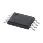
| 供应商器件封装 | 8-TSSOP |
| 其它名称 | 497-6358-6 |
| 其它有关文件 | http://www.st.com/web/catalog/mmc/FM76/CL1276/SC112/PF104066?referrer=70071840 |
| 包装 | Digi-Reel® |
| 商标 | STMicroelectronics |
| 存储器类型 | EEPROM |
| 存储容量 | 512 kbit |
| 安装风格 | SMD/SMT |
| 封装 | Reel |
| 封装/外壳 | 8-TSSOP(0.173",4.40mm 宽) |
| 封装/箱体 | TSSOP-8 |
| 工作温度 | -40°C ~ 85°C |
| 工作电流 | 2.5 mA |
| 工作电源电压 | 2.5 V, 3.3 V, 5 V |
| 工厂包装数量 | 4000 |
| 接口 | SPI 串行 |
| 接口类型 | SPI |
| 数据保留 | 40 yr |
| 最大工作温度 | + 85 C |
| 最大工作电流 | 3 mA |
| 最大时钟频率 | 2 MHz |
| 最小工作温度 | - 40 C |
| 标准包装 | 1 |
| 格式-存储器 | EEPROMs - 串行 |
| 电压-电源 | 1.8 V ~ 5.5 V |
| 电源电压-最大 | 5.5 V |
| 电源电压-最小 | 1.8 V |
| 系列 | M95512-R |
| 组织 | 64 k x 8 |
| 访问时间 | 80 ns |
| 速度 | 5MHz |


- 商务部:美国ITC正式对集成电路等产品启动337调查
- 曝三星4nm工艺存在良率问题 高通将骁龙8 Gen1或转产台积电
- 太阳诱电将投资9.5亿元在常州建新厂生产MLCC 预计2023年完工
- 英特尔发布欧洲新工厂建设计划 深化IDM 2.0 战略
- 台积电先进制程称霸业界 有大客户加持明年业绩稳了
- 达到5530亿美元!SIA预计今年全球半导体销售额将创下新高
- 英特尔拟将自动驾驶子公司Mobileye上市 估值或超500亿美元
- 三星加码芯片和SET,合并消费电子和移动部门,撤换高东真等 CEO
- 三星电子宣布重大人事变动 还合并消费电子和移动部门
- 海关总署:前11个月进口集成电路产品价值2.52万亿元 增长14.8%


_renders/MR4A16BCYS35.jpg)

PDF Datasheet 数据手册内容提取
M95512-W M95512-R M95512-DF 512-Kbit serial SPI bus EEPROM Datasheet - production data Features • Compatible with the serial peripheral interface (SPI) bus • Memory array SO8 (MN) – 512 Kbit (64 Kbytes) of EEPROM 150 mil width – Page size: 128 bytes • Write – Byte Write within 5 ms – Page Write within 5 ms • Additional write lockable page (Identification TSSOP8 (DW) page) 169 mil width • Write protect: quarter, half or whole memory array • High-speed clock: 16 MHz • Single supply voltage: – 2.5 V to 5.5 V for M95512-W – 1.8 V to 5.5 V for M95512-R UFDFPN8 (MC) – 1.7 V to 5.5 V for M95512-DF DFN8 2 x 3 mm • Operating temperature range: from -40 °C up to +85 °C • Enhanced ESD protection • More than 4 million Write cycles • More than 200-year data retention WLCSP (CS) • Packages: – SO8 (ECOPACK2®) – TSSOP8 (ECOPACK2®) – UFDFPN8 (ECOPACK2®) – WLCSP (ECOPACK2®) November 2018 DS4192 Rev 23 1/54 This is information on a product in full production. www.st.com
Contents M95512-W M95512-R M95512-DF Contents 1 Description . . . . . . . . . . . . . . . . . . . . . . . . . . . . . . . . . . . . . . . . . . . . . . . . . 6 2 Memory organization . . . . . . . . . . . . . . . . . . . . . . . . . . . . . . . . . . . . . . . . 8 3 Signal description . . . . . . . . . . . . . . . . . . . . . . . . . . . . . . . . . . . . . . . . . . . 9 3.1 Serial data output (Q) . . . . . . . . . . . . . . . . . . . . . . . . . . . . . . . . . . . . . . . . . 9 3.2 Serial data input (D) . . . . . . . . . . . . . . . . . . . . . . . . . . . . . . . . . . . . . . . . . . 9 3.3 Serial clock (C) . . . . . . . . . . . . . . . . . . . . . . . . . . . . . . . . . . . . . . . . . . . . . . 9 3.4 Chip select (S) . . . . . . . . . . . . . . . . . . . . . . . . . . . . . . . . . . . . . . . . . . . . . . 9 3.5 Hold (HOLD) . . . . . . . . . . . . . . . . . . . . . . . . . . . . . . . . . . . . . . . . . . . . . . . . 9 3.6 Write protect (W) . . . . . . . . . . . . . . . . . . . . . . . . . . . . . . . . . . . . . . . . . . . 10 3.7 V supply voltage . . . . . . . . . . . . . . . . . . . . . . . . . . . . . . . . . . . . . . . . . . 10 CC 3.8 V ground . . . . . . . . . . . . . . . . . . . . . . . . . . . . . . . . . . . . . . . . . . . . . . . . 10 SS 4 Connecting to the SPI bus . . . . . . . . . . . . . . . . . . . . . . . . . . . . . . . . . . . 11 4.1 SPI modes . . . . . . . . . . . . . . . . . . . . . . . . . . . . . . . . . . . . . . . . . . . . . . . . 12 5 Operating features . . . . . . . . . . . . . . . . . . . . . . . . . . . . . . . . . . . . . . . . . 13 5.1 Supply voltage (V ) . . . . . . . . . . . . . . . . . . . . . . . . . . . . . . . . . . . . . . . . 13 CC 5.1.1 Operating supply voltage (V ) . . . . . . . . . . . . . . . . . . . . . . . . . . . . . . . 13 CC 5.1.2 Device reset . . . . . . . . . . . . . . . . . . . . . . . . . . . . . . . . . . . . . . . . . . . . . . 13 5.1.3 Power-up conditions . . . . . . . . . . . . . . . . . . . . . . . . . . . . . . . . . . . . . . . 13 5.1.4 Power-down . . . . . . . . . . . . . . . . . . . . . . . . . . . . . . . . . . . . . . . . . . . . . . 14 5.2 Active Power and Standby Power modes . . . . . . . . . . . . . . . . . . . . . . . . 14 5.3 Hold condition . . . . . . . . . . . . . . . . . . . . . . . . . . . . . . . . . . . . . . . . . . . . . . 14 5.4 Status register . . . . . . . . . . . . . . . . . . . . . . . . . . . . . . . . . . . . . . . . . . . . . 15 5.5 Data protection and protocol control . . . . . . . . . . . . . . . . . . . . . . . . . . . . 15 6 Instructions . . . . . . . . . . . . . . . . . . . . . . . . . . . . . . . . . . . . . . . . . . . . . . . 16 6.1 Write enable (WREN) . . . . . . . . . . . . . . . . . . . . . . . . . . . . . . . . . . . . . . . . 17 6.2 Write disable (WRDI) . . . . . . . . . . . . . . . . . . . . . . . . . . . . . . . . . . . . . . . . 18 6.3 Read Status Register (RDSR) . . . . . . . . . . . . . . . . . . . . . . . . . . . . . . . . . 19 6.3.1 WIP bit . . . . . . . . . . . . . . . . . . . . . . . . . . . . . . . . . . . . . . . . . . . . . . . . . . 19 2/54 DS4192 Rev 23
M95512-W M95512-R M95512-DF Contents 6.3.2 WEL bit . . . . . . . . . . . . . . . . . . . . . . . . . . . . . . . . . . . . . . . . . . . . . . . . . 19 6.3.3 BP1, BP0 bits . . . . . . . . . . . . . . . . . . . . . . . . . . . . . . . . . . . . . . . . . . . . . 19 6.3.4 SRWD bit . . . . . . . . . . . . . . . . . . . . . . . . . . . . . . . . . . . . . . . . . . . . . . . . 20 6.4 Write Status Register (WRSR) . . . . . . . . . . . . . . . . . . . . . . . . . . . . . . . . . 21 6.5 Read from Memory Array (READ) . . . . . . . . . . . . . . . . . . . . . . . . . . . . . . 23 6.6 Write to Memory Array (WRITE) . . . . . . . . . . . . . . . . . . . . . . . . . . . . . . . 24 6.6.1 Cycling with error correction code (ECC x4) . . . . . . . . . . . . . . . . . . . . . 26 6.7 Read Identification page (available only in M95512-D devices) . . . . . . . . 27 6.8 Write Identification Page (available only in M95512-D devices) . . . . . . . 28 6.9 Read Lock Status (available only in M95512-D devices) . . . . . . . . . . . . . 29 6.10 Lock ID (available only in M95512-D devices) . . . . . . . . . . . . . . . . . . . . . 30 7 Power-up and delivery state . . . . . . . . . . . . . . . . . . . . . . . . . . . . . . . . . . 31 7.1 Power-up state . . . . . . . . . . . . . . . . . . . . . . . . . . . . . . . . . . . . . . . . . . . . . 31 7.2 Initial delivery state . . . . . . . . . . . . . . . . . . . . . . . . . . . . . . . . . . . . . . . . . . 31 8 Maximum ratings . . . . . . . . . . . . . . . . . . . . . . . . . . . . . . . . . . . . . . . . . . . 32 9 DC and AC parameters . . . . . . . . . . . . . . . . . . . . . . . . . . . . . . . . . . . . . . 33 10 Package information . . . . . . . . . . . . . . . . . . . . . . . . . . . . . . . . . . . . . . . . 43 10.1 SO8N package information . . . . . . . . . . . . . . . . . . . . . . . . . . . . . . . . . . . 43 10.2 TSSOP8 package information . . . . . . . . . . . . . . . . . . . . . . . . . . . . . . . . . 45 10.3 UFDFPN8 (DFN8) package information . . . . . . . . . . . . . . . . . . . . . . . . . . 46 10.4 WLCSP8 package information . . . . . . . . . . . . . . . . . . . . . . . . . . . . . . . . . 47 11 Ordering information . . . . . . . . . . . . . . . . . . . . . . . . . . . . . . . . . . . . . . . 49 12 Revision history . . . . . . . . . . . . . . . . . . . . . . . . . . . . . . . . . . . . . . . . . . . 51 DS4192 Rev 23 3/54 3
List of tables M95512-W M95512-R M95512-DF List of tables Table 1. Signal names . . . . . . . . . . . . . . . . . . . . . . . . . . . . . . . . . . . . . . . . . . . . . . . . . . . . . . . . . . . . 6 Table 2. Signals vs. bump position. . . . . . . . . . . . . . . . . . . . . . . . . . . . . . . . . . . . . . . . . . . . . . . . . . . 7 Table 3. Write-protected block size . . . . . . . . . . . . . . . . . . . . . . . . . . . . . . . . . . . . . . . . . . . . . . . . . 15 Table 4. Instruction set. . . . . . . . . . . . . . . . . . . . . . . . . . . . . . . . . . . . . . . . . . . . . . . . . . . . . . . . . . . 16 Table 5. Significant bits within the two address bytes . . . . . . . . . . . . . . . . . . . . . . . . . . . . . . . . . . . 16 Table 6. Status register format. . . . . . . . . . . . . . . . . . . . . . . . . . . . . . . . . . . . . . . . . . . . . . . . . . . . . 20 Table 7. Protection modes . . . . . . . . . . . . . . . . . . . . . . . . . . . . . . . . . . . . . . . . . . . . . . . . . . . . . . . . 22 Table 8. Absolute maximum ratings. . . . . . . . . . . . . . . . . . . . . . . . . . . . . . . . . . . . . . . . . . . . . . . . . 32 Table 9. Operating conditions (M95512-W, device grade 6) . . . . . . . . . . . . . . . . . . . . . . . . . . . . . . 33 Table 10. Operating conditions (M95512-R, device grade 6). . . . . . . . . . . . . . . . . . . . . . . . . . . . . . . 33 Table 11. Operating conditions (M95512-DF, device grade 6). . . . . . . . . . . . . . . . . . . . . . . . . . . . . . 33 Table 12. AC measurement conditions. . . . . . . . . . . . . . . . . . . . . . . . . . . . . . . . . . . . . . . . . . . . . . . . 33 Table 13. Cycling performance by groups of four bytes. . . . . . . . . . . . . . . . . . . . . . . . . . . . . . . . . . . 34 Table 14. Memory cell data retention. . . . . . . . . . . . . . . . . . . . . . . . . . . . . . . . . . . . . . . . . . . . . . . . . 34 Table 15. Capacitance . . . . . . . . . . . . . . . . . . . . . . . . . . . . . . . . . . . . . . . . . . . . . . . . . . . . . . . . . . . . 34 Table 16. DC characteristics (previous M95512-W products, device grade 6). . . . . . . . . . . . . . . . . . 35 Table 17. DC characteristics (M95512-W products, device grade 6). . . . . . . . . . . . . . . . . . . . . . . . . 36 Table 18. DC characteristics (M95512-R, device grade 6). . . . . . . . . . . . . . . . . . . . . . . . . . . . . . . . . 37 Table 19. DC characteristics (M95512-DF products, device grade 6) . . . . . . . . . . . . . . . . . . . . . . . . 38 Table 20. AC characteristics (previous M95512-W products, device grade 6). . . . . . . . . . . . . . . . . . 39 Table 21. AC characteristics (M95512-W products, device grade 6) . . . . . . . . . . . . . . . . . . . . . . . . . 40 Table 22. AC characteristics (M95512-R and M95512-DF, device grade 6) . . . . . . . . . . . . . . . . . . . 41 Table 23. SO8N – 8-lead plastic small outline, 150 mils body width, package mechanical data. . . . . . . . . . . . . . . . . . . . . . . . . . . . . . . . . . . . . . . . . . . . . . . . . . 43 Table 24. TSSOP8 – 8-lead thin shrink small outline, 3 x 4.4 mm, 0.65 mm pitch, package mechanical data. . . . . . . . . . . . . . . . . . . . . . . . . . . . . . . . . . . . . . . . . . . . . . . . . . 45 Table 25. UFDFPN8 (DFN8) - 8-lead, 2 × 3 mm, 0.5 mm pitch ultra thin profile fine pitch dual flat package mechanical data . . . . . . . . . . . . . . . . . . . . . . . . . . . . . . . . . . . 46 Table 26. WLCSP - 8 bumps, 1.289 x 1.955 mm, 0.5 mm pitch wafer level chip scale package mechanical data. . . . . . . . . . . . . . . . . . . . . . . . . . . . . . . . . . . . . . . . . . . . . . . . . . 48 Table 27. Ordering information scheme. . . . . . . . . . . . . . . . . . . . . . . . . . . . . . . . . . . . . . . . . . . . . . . 49 Table 28. Document revision history . . . . . . . . . . . . . . . . . . . . . . . . . . . . . . . . . . . . . . . . . . . . . . . . . 51 4/54 DS4192 Rev 23
M95512-W M95512-R M95512-DF List of figures List of figures Figure 1. Logic diagram. . . . . . . . . . . . . . . . . . . . . . . . . . . . . . . . . . . . . . . . . . . . . . . . . . . . . . . . . . . . 6 Figure 2. 8-pin package connections (top view) . . . . . . . . . . . . . . . . . . . . . . . . . . . . . . . . . . . . . . . . . 7 Figure 3. WLCSP connections for M95512-DFCS6TP/K . . . . . . . . . . . . . . . . . . . . . . . . . . . . . . . . . . 7 Figure 4. Block diagram. . . . . . . . . . . . . . . . . . . . . . . . . . . . . . . . . . . . . . . . . . . . . . . . . . . . . . . . . . . . 8 Figure 5. Bus master and memory devices on the SPI bus. . . . . . . . . . . . . . . . . . . . . . . . . . . . . . . . 11 Figure 6. SPI modes supported. . . . . . . . . . . . . . . . . . . . . . . . . . . . . . . . . . . . . . . . . . . . . . . . . . . . . 12 Figure 7. Hold condition activation. . . . . . . . . . . . . . . . . . . . . . . . . . . . . . . . . . . . . . . . . . . . . . . . . . . 14 Figure 8. Write enable (WREN) sequence. . . . . . . . . . . . . . . . . . . . . . . . . . . . . . . . . . . . . . . . . . . . . 17 Figure 9. Write disable (WRDI) sequence. . . . . . . . . . . . . . . . . . . . . . . . . . . . . . . . . . . . . . . . . . . . . 18 Figure 10. Read Status Register (RDSR) sequence. . . . . . . . . . . . . . . . . . . . . . . . . . . . . . . . . . . . . . 19 Figure 11. Write Status Register (WRSR) sequence. . . . . . . . . . . . . . . . . . . . . . . . . . . . . . . . . . . . . . 21 Figure 12. Read from Memory Array (READ) sequence . . . . . . . . . . . . . . . . . . . . . . . . . . . . . . . . . . . 23 Figure 13. Byte Write (WRITE) sequence . . . . . . . . . . . . . . . . . . . . . . . . . . . . . . . . . . . . . . . . . . . . . . 24 Figure 14. Page Write (WRITE) sequence . . . . . . . . . . . . . . . . . . . . . . . . . . . . . . . . . . . . . . . . . . . . . 25 Figure 15. Read Identification page sequence . . . . . . . . . . . . . . . . . . . . . . . . . . . . . . . . . . . . . . . . . . 27 Figure 16. Write Identification Page sequence . . . . . . . . . . . . . . . . . . . . . . . . . . . . . . . . . . . . . . . . . . 28 Figure 17. Read Lock Status sequence. . . . . . . . . . . . . . . . . . . . . . . . . . . . . . . . . . . . . . . . . . . . . . . . 29 Figure 18. Lock ID sequence. . . . . . . . . . . . . . . . . . . . . . . . . . . . . . . . . . . . . . . . . . . . . . . . . . . . . . . . 30 Figure 19. AC measurement I/O waveform. . . . . . . . . . . . . . . . . . . . . . . . . . . . . . . . . . . . . . . . . . . . . 33 Figure 20. Serial input timing. . . . . . . . . . . . . . . . . . . . . . . . . . . . . . . . . . . . . . . . . . . . . . . . . . . . . . . . 42 Figure 21. Hold timing . . . . . . . . . . . . . . . . . . . . . . . . . . . . . . . . . . . . . . . . . . . . . . . . . . . . . . . . . . . . . 42 Figure 22. Serial output timing. . . . . . . . . . . . . . . . . . . . . . . . . . . . . . . . . . . . . . . . . . . . . . . . . . . . . . . 42 Figure 23. SO8N – 8-lead plastic small outline, 150 mils body width, package outline. . . . . . . . . . . . 43 Figure 24. SO8N – 8-lead plastic small outline, 150 mils body width, package recommended footprint . . . . . . . . . . . . . . . . . . . . . . . . . . . . . . . . . . . . . . . . . . . . 44 Figure 25. TSSOP8 – 8-lead thin shrink small outline, 3 x 4.4 mm, 0.65 mm pitch, package outline. . . . . . . . . . . . . . . . . . . . . . . . . . . . . . . . . . . . . . . . . . . . . . . . . . . . . . . . . . 45 Figure 26. UFDFPN8 (DFN8) - 8-lead, 2 × 3 mm, 0.5 mm pitch ultra thin profile fine pitch dual flat package outline . . . . . . . . . . . . . . . . . . . . . . . . . . . . . . . . . . . . . . . . . . . 46 Figure 27. WLCSP - 8 bumps, 1.289 x 1.955 mm, 0.5 mm pitch wafer level chip scale package outline. . . . . . . . . . . . . . . . . . . . . . . . . . . . . . . . . . . . . . . . . . . . . . . . . . . . . . . . . . 47 Figure 28. WLCSP - 8 bumps, 1.289 x 1.955 mm, 0.5 mm pitch wafer level chip scale package recommended footprint . . . . . . . . . . . . . . . . . . . . . . . . . . . . . . . . . . . . . . . . . . . . 48 DS4192 Rev 23 5/54 5
Description M95512-W M95512-R M95512-DF 1 Description The M95512 devices are Electrically Erasable PROgrammable Memories (EEPROMs) organized as 65536 x 8 bits, accessed through the SPI bus. The M95512-W can operate with a supply voltage from 2.5 V to 5.5 V, the M95512-R can operate with a supply voltage from 1.8 V to 5.5 V and the M95512-DF can operate with a supply voltage from 1.7 V to 5.5 V, over an ambient temperature range of -40 °C / +85 °C. The M95512-D offers an additional page, named the Identification page (128 bytes). The Identification page can be used to store sensitive application parameters that can be (later) permanently locked in read-only mode. Figure 1. Logic diagram (cid:57) (cid:38)(cid:38) (cid:39) (cid:52) (cid:38) (cid:54) (cid:48)(cid:28)(cid:24)(cid:91)(cid:91)(cid:91) (cid:58) (cid:43)(cid:50)(cid:47)(cid:39) (cid:57) (cid:54)(cid:54) (cid:48)(cid:54)(cid:23)(cid:24)(cid:23)(cid:20)(cid:22)(cid:57)(cid:20) The SPI bus signals are C, D and Q, as shown in Figure 1 and Table 1. The device is selected when Chip select (S) is driven low. Communications with the device can be interrupted when the HOLD is driven low. Table 1. Signal names Signal name Function Direction C Serial clock Input D Serial data input Input Q Serial data output Output S Chip select Input W Write protect Input HOLD Hold Input V Supply voltage - CC V Ground - SS 6/54 DS4192 Rev 23
M95512-W M95512-R M95512-DF Description Figure 2. 8-pin package connections (top view) (cid:48)(cid:28)(cid:24)(cid:91)(cid:91)(cid:91) (cid:54) (cid:20) (cid:27) (cid:57) (cid:38)(cid:38) (cid:52) (cid:21) (cid:26) (cid:43)(cid:50)(cid:47)(cid:39) (cid:58) (cid:22) (cid:25) (cid:38) (cid:57) (cid:23) (cid:24) (cid:39) (cid:54)(cid:54) (cid:48)(cid:54)(cid:24)(cid:20)(cid:24)(cid:26)(cid:28)(cid:57)(cid:20) 1. See Section 10: Package information for package dimensions, and how to identify Pin 1. Figure 3. WLCSP connections for M95512-DFCS6TP/K (cid:20) (cid:21) (cid:22) (cid:22) (cid:21) (cid:20) (cid:36) (cid:39) (cid:57)(cid:38)(cid:38) (cid:57)(cid:38)(cid:38) (cid:39) (cid:36) (cid:37) (cid:38) (cid:38) (cid:37) (cid:38) (cid:58) (cid:43)(cid:50)(cid:47)(cid:39) (cid:43)(cid:50)(cid:47)(cid:39) (cid:58) (cid:38) (cid:39) (cid:52) (cid:52) (cid:39) (cid:40) (cid:57)(cid:54)(cid:54) (cid:54) (cid:54) (cid:57)(cid:54)(cid:54) (cid:40) (cid:48)(cid:68)(cid:85)(cid:78)(cid:76)(cid:81)(cid:74)(cid:3)(cid:86)(cid:76)(cid:71)(cid:72)(cid:3)(cid:11)(cid:87)(cid:82)(cid:83)(cid:3)(cid:89)(cid:76)(cid:72)(cid:90)(cid:12) (cid:37)(cid:88)(cid:80)(cid:83)(cid:3)(cid:86)(cid:76)(cid:71)(cid:72)(cid:3)(cid:11)(cid:69)(cid:82)(cid:87)(cid:87)(cid:82)(cid:80)(cid:3)(cid:89)(cid:76)(cid:72)(cid:90)(cid:12) (cid:48)(cid:54)(cid:24)(cid:20)(cid:25)(cid:20)(cid:22)(cid:57)(cid:20) Table 2. Signals vs. bump position Position A B C D E 1 D - W - V SS 2 - C - Q - 3 V - HOLD - S CC DS4192 Rev 23 7/54 42
Memory organization M95512-W M95512-R M95512-DF 2 Memory organization The memory is organized as shown in the following figure. Figure 4. Block diagram (cid:43)(cid:50)(cid:47)(cid:39) (cid:43)(cid:76)(cid:74)(cid:75)(cid:3)(cid:89)(cid:82)(cid:79)(cid:87)(cid:68)(cid:74)(cid:72)(cid:3) (cid:58) (cid:38)(cid:82)(cid:81)(cid:87)(cid:85)(cid:82)(cid:79)(cid:3)(cid:79)(cid:82)(cid:74)(cid:76)(cid:70) (cid:74)(cid:72)(cid:81)(cid:72)(cid:85)(cid:68)(cid:87)(cid:82)(cid:85) (cid:54) (cid:38) (cid:39) (cid:44)(cid:18)(cid:50)(cid:3)(cid:86)(cid:75)(cid:76)(cid:73)(cid:87)(cid:3)(cid:85)(cid:72)(cid:74)(cid:76)(cid:86)(cid:87)(cid:72)(cid:85) (cid:52) (cid:36)(cid:71)(cid:71)(cid:85)(cid:72)(cid:86)(cid:86)(cid:3)(cid:85)(cid:72)(cid:74)(cid:76)(cid:86)(cid:87)(cid:72)(cid:85) (cid:39)(cid:68)(cid:87)(cid:68)(cid:3)(cid:85)(cid:72)(cid:74)(cid:76)(cid:86)(cid:87)(cid:72)(cid:85) (cid:68)(cid:81)(cid:71)(cid:3)(cid:70)(cid:82)(cid:88)(cid:81)(cid:87)(cid:72)(cid:85) (cid:54)(cid:87)(cid:68)(cid:87)(cid:88)(cid:86)(cid:3) (cid:85)(cid:72)(cid:74)(cid:76)(cid:86)(cid:87)(cid:72)(cid:85) (cid:20)(cid:18)(cid:23) (cid:72)(cid:85) (cid:71) (cid:40)(cid:40)(cid:51)(cid:53)(cid:50)(cid:48)(cid:3) (cid:82) (cid:20)(cid:18)(cid:21) (cid:70) (cid:72) (cid:68)(cid:85)(cid:72)(cid:68) (cid:71) (cid:60)(cid:3) (cid:20)(cid:3)(cid:83)(cid:68)(cid:74)(cid:72) (cid:44)(cid:71)(cid:72)(cid:81)(cid:87)(cid:76)(cid:73)(cid:76)(cid:70)(cid:68)(cid:87)(cid:76)(cid:82)(cid:81)(cid:3)(cid:83)(cid:68)(cid:74)(cid:72) (cid:59)(cid:3)(cid:71)(cid:72)(cid:70)(cid:82)(cid:71)(cid:72)(cid:85) (cid:48)(cid:54)(cid:20)(cid:28)(cid:26)(cid:22)(cid:22)(cid:57)(cid:21) 8/54 DS4192 Rev 23
M95512-W M95512-R M95512-DF Signal description 3 Signal description During all operations, V must be held stable and within the specified valid range: CC V (min) to V (max). CC CC All of the input and output signals must be held high or low (according to voltages of V , IH V , V or V , as specified in Section 9: DC and AC parameters). These signals are OH IL OL described next. 3.1 Serial data output (Q) This output signal is used to transfer data serially out of the device. Data is shifted out on the falling edge of Serial clock (C). 3.2 Serial data input (D) This input signal is used to transfer data serially into the device. It receives instructions, addresses, and the data to be written. Values are latched on the rising edge of Serial clock (C). 3.3 Serial clock (C) This input signal provides the timing of the serial interface. Instructions, addresses, or data present at Serial data input (D) are latched on the rising edge of Serial clock (C). Data on Serial data output (Q) change from the falling edge of Serial clock (C). 3.4 Chip select (S) When this input signal is high, the device is deselected and Serial data output (Q) is at high impedance. The device is in the Standby Power mode, unless an internal Write cycle is in progress. Driving Chip select (S) low selects the device, placing it in the Active Power mode. After power-up, a falling edge on Chip select (S) is required prior to the start of any instruction. 3.5 Hold (HOLD) The Hold (HOLD) signal is used to pause any serial communications with the device without deselecting the device. During the Hold condition, the Serial data output (Q) is high impedance, and Serial data input (D) and Serial clock (C) are Don’t Care. To start the Hold condition, the device must be selected, with Chip select (S) driven low. DS4192 Rev 23 9/54 42
Signal description M95512-W M95512-R M95512-DF 3.6 Write protect (W) The main purpose of this input signal is to freeze the size of the area of memory that is protected against Write instructions (as specified by the values in the BP1 and BP0 bits of the Status register). This pin must be driven either high or low, and must be stable during all Write instructions. 3.7 V supply voltage CC V is the supply voltage. CC 3.8 V ground SS V is the reference for all signals, including the V supply voltage. SS CC 10/54 DS4192 Rev 23
M95512-W M95512-R M95512-DF Connecting to the SPI bus 4 Connecting to the SPI bus All instructions, addresses and input data bytes are shifted in to the device, most significant bit first. The Serial data input (D) is sampled on the first rising edge of the Serial clock (C) after Chip select (S) goes low. All output data bytes are shifted out of the device, most significant bit first. The Serial data output (Q) is latched on the first falling edge of the Serial clock (C) after the instruction (such as the Read from Memory Array and Read Status Register instructions) have been clocked into the device. Figure 5. Bus master and memory devices on the SPI bus (cid:57)(cid:54)(cid:54) (cid:57)(cid:38)(cid:38) (cid:53) (cid:54)(cid:39)(cid:50) (cid:54)(cid:51)(cid:44)(cid:3)(cid:44)(cid:81)(cid:87)(cid:72)(cid:85)(cid:73)(cid:68)(cid:70)(cid:72)(cid:3)(cid:90)(cid:76)(cid:87)(cid:75) (cid:54)(cid:39)(cid:44) (cid:11)(cid:38)(cid:51)(cid:50)(cid:47)(cid:15)(cid:3)(cid:38)(cid:51)(cid:43)(cid:36)(cid:12)(cid:3)(cid:32) (cid:11)(cid:19)(cid:15)(cid:3)(cid:19)(cid:12)(cid:3)(cid:82)(cid:85)(cid:3)(cid:11)(cid:20)(cid:15)(cid:3)(cid:20)(cid:12) (cid:54)(cid:38)(cid:46) (cid:38) (cid:52) (cid:39) (cid:57)(cid:38)(cid:38) (cid:38) (cid:52) (cid:39) (cid:57)(cid:38)(cid:38) (cid:38) (cid:52) (cid:39) (cid:57)(cid:38)(cid:38) (cid:54)(cid:51)(cid:44)(cid:3)(cid:37)(cid:88)(cid:86)(cid:3)(cid:48)(cid:68)(cid:86)(cid:87)(cid:72)(cid:85) (cid:57)(cid:54)(cid:54) (cid:57)(cid:54)(cid:54) (cid:57)(cid:54)(cid:54) (cid:54)(cid:51)(cid:44)(cid:3)(cid:48)(cid:72)(cid:80)(cid:82)(cid:85)(cid:92) (cid:54)(cid:51)(cid:44)(cid:3)(cid:48)(cid:72)(cid:80)(cid:82)(cid:85)(cid:92) (cid:54)(cid:51)(cid:44)(cid:3)(cid:48)(cid:72)(cid:80)(cid:82)(cid:85)(cid:92) (cid:53) (cid:53) (cid:53) (cid:39)(cid:72)(cid:89)(cid:76)(cid:70)(cid:72) (cid:39)(cid:72)(cid:89)(cid:76)(cid:70)(cid:72) (cid:39)(cid:72)(cid:89)(cid:76)(cid:70)(cid:72) (cid:38)(cid:54)(cid:22) (cid:38)(cid:54)(cid:21) (cid:38)(cid:54)(cid:20) (cid:54) (cid:58) (cid:43)(cid:50)(cid:47)(cid:39) (cid:54) (cid:58) (cid:43)(cid:50)(cid:47)(cid:39) (cid:54) (cid:58) (cid:43)(cid:50)(cid:47)(cid:39) (cid:36)(cid:44)(cid:20)(cid:21)(cid:27)(cid:22)(cid:25)(cid:69) 1. The Write protect (W) and Hold (HOLD) signals should be driven, high or low as appropriate. Figure 5 shows an example of three memory devices connected to an SPI bus master. Only one memory device is selected at a time, so only one memory device drives the Serial data output (Q) line at a time. The other memory devices are high impedance. The pull-up resistor R (represented in Figure 5) ensures that a device is not selected if the Bus Master leaves the S line in the high impedance state. In applications where the Bus Master may leave all SPI bus lines in high impedance at the same time (for example, if the Bus Master is reset during the transmission of an instruction), the clock line (C) must be connected to an external pull-down resistor so that, if all inputs/outputs become high impedance, the C line is pulled low (while the S line is pulled high): this ensures that S and C do not become high at the same time, and so, that the t requirement is met. The typical value of R is 100 kΩ. SHCH DS4192 Rev 23 11/54 42
Connecting to the SPI bus M95512-W M95512-R M95512-DF 4.1 SPI modes These devices can be driven by a microcontroller with its SPI peripheral running in either of the following two modes: • CPOL = 0, CPHA = 0 • CPOL = 1, CPHA = 1 For these two modes, input data is latched in on the rising edge of Serial clock (C), and output data is available from the falling edge of Serial clock (C). The difference between the two modes, as shown in Figure 6, is the clock polarity when the bus master is in Stand-by mode and not transferring data: • C remains at 0 for (CPOL = 0, CPHA = 0) • C remains at 1 for (CPOL = 1, CPHA = 1) Figure 6. SPI modes supported (cid:38)(cid:51)(cid:50)(cid:47) (cid:38)(cid:51)(cid:43)(cid:36) (cid:19) (cid:19) (cid:35) (cid:20) (cid:20) (cid:35) (cid:36) (cid:48)(cid:54)(cid:37) (cid:49) (cid:48)(cid:54)(cid:37) (cid:48)(cid:54)(cid:23)(cid:21)(cid:25)(cid:26)(cid:23)(cid:57)(cid:21) 12/54 DS4192 Rev 23
M95512-W M95512-R M95512-DF Operating features 5 Operating features 5.1 Supply voltage (V ) CC 5.1.1 Operating supply voltage (V ) CC Prior to selecting the memory and issuing instructions to it, a valid and stable V voltage CC within the specified [V (min), V (max)] range must be applied (see Operating conditions CC CC in Section 9: DC and AC parameters). This voltage must remain stable and valid until the end of the transmission of the instruction and, for a Write instruction, until the completion of the internal write cycle (t ). In order to secure a stable DC supply voltage, it is W recommended to decouple the V line with a suitable capacitor (usually in the range CC between 10 and 100 nF) close to the V / V device pins. CC SS 5.1.2 Device reset In order to prevent erroneous instruction decoding and inadvertent Write operations during power-up, a power-on-reset (POR) circuit is included. At power-up, the device does not respond to any instruction until VCC reaches the POR threshold voltage. This threshold is lower than the minimum V operating voltage (see Operating conditions in Section 9). CC At power-up, when V passes over the POR threshold, the device is reset and is in the CC following state: • in Standby Power mode, • deselected, • Status register values: – The Write enable latch (WEL) bit is reset to 0. – The Write in progress (WIP) bit is reset to 0. – The SRWD, BP1 and BP0 bits remain unchanged (non-volatile bits). It is important to note that the device must not be accessed until V reaches a valid and CC stable level within the specified [V (min), V (max)] range, as defined under Operating CC CC conditions in Section 9. 5.1.3 Power-up conditions When the power supply is turned on, V rises continuously from V to V . During this CC SS CC time, the Chip select (S) line is not allowed to float but should follow the V voltage. It is CC therefore recommended to connect the S line to V via a suitable pull-up resistor (see CC Figure 5). In addition, the Chip select (S) input offers a built-in safety feature, as the S input is edge-sensitive as well as level-sensitive: after power-up, the device does not become selected until a falling edge has first been detected on Chip select (S). This ensures that Chip select (S) must have been high, prior to going low to start the first operation. The V voltage has to rise continuously from 0 V up to the minimum V operating voltage CC CC defined under Operating conditions in Section 9. DS4192 Rev 23 13/54 42
Operating features M95512-W M95512-R M95512-DF 5.1.4 Power-down During power-down (continuous decrease of the V supply voltage below the minimum CC V operating voltage defined under Operating conditions in Section 9), the device must be: CC • deselected (Chip select S should be allowed to follow the voltage applied on V ), CC • in Standby Power mode (there should not be any internal write cycle in progress). 5.2 Active Power and Standby Power modes When Chip select (S) is low, the device is selected, and in the Active Power mode. The device consumes I . CC When Chip select (S) is high, the device is deselected. If a Write cycle is not currently in progress, the device then goes into the Standby Power mode, and the device consumption drops to I , as specified in DC characteristics (see Section 9). CC1 5.3 Hold condition The Hold (HOLD) signal is used to pause any serial communications with the device without resetting the clocking sequence. To enter the Hold condition, the device must be selected, with Chip select (S) low. During the Hold condition, the Serial data output (Q) is high impedance, and the Serial data input (D) and the Serial clock (C) are Don’t Care. Normally, the device is kept selected for the whole duration of the Hold condition. Deselecting the device while it is in the Hold condition has the effect of resetting the state of the device: this mechanism can be used, if required, to reset the ongoing processes(a) (b). Figure 7. Hold condition activation (cid:38) (cid:43)(cid:50)(cid:47)(cid:39) (cid:43)(cid:82)(cid:79)(cid:71)(cid:3) (cid:43)(cid:82)(cid:79)(cid:71)(cid:3) (cid:70)(cid:82)(cid:81)(cid:71)(cid:76)(cid:87)(cid:76)(cid:82)(cid:81) (cid:70)(cid:82)(cid:81)(cid:71)(cid:76)(cid:87)(cid:76)(cid:82)(cid:81) (cid:48)(cid:54)(cid:23)(cid:26)(cid:21)(cid:27)(cid:20)(cid:57)(cid:20) The Hold condition starts when the Hold (HOLD) signal is driven low when Serial clock (C) is already low (as shown in Figure 7). Figure 7 also shows what happens if the rising and falling edges are not timed to coincide with Serial clock (C) being low. a. This resets the internal logic, except the WEL and WIP bits of the Status register. b. In the specific case where the device has moved in a Write command (Inst + Address + data bytes, each data byte being exactly 8 bits), deselecting the device also triggers the Write cycle of this decoded command. 14/54 DS4192 Rev 23
M95512-W M95512-R M95512-DF Operating features 5.4 Status register The Status register contains a number of status and control bits that can be read or set (as appropriate) by specific instructions. See Section 6.3: Read Status Register (RDSR) for a detailed description of the Status register bits. 5.5 Data protection and protocol control The device features the following data protection mechanisms: • Before accepting the execution of the Write and Write Status Register instructions, the device checks whether the number of clock pulses comprised in the instructions is a multiple of eight. • All instructions that modify data must be preceded by a Write Enable (WREN) instruction to set the Write enable latch (WEL) bit. • The Block protect (BP1, BP0) bits in the Status register are used to configure part of the memory as read-only. • The Write protect (W) signal is used to protect the Block protect (BP1, BP0) bits in the Status register. For any instruction to be accepted, and executed, Chip select (S) must be driven high after the rising edge of Serial clock (C) for the last bit of the instruction, and before the next rising edge of Serial clock (C). Two points should be noted in the previous sentence: • The “last bit of the instruction” can be the eighth bit of the instruction code, or the eighth bit of a data byte, depending on the instruction (except for Read Status Register (RDSR) and Read (READ) instructions). • The “next rising edge of Serial clock (C)” might (or might not) be the next bus transaction for some other device on the SPI bus. Table 3. Write-protected block size Status register bits Protected block Protected array addresses BP1 BP0 0 0 None None 0 1 Upper quarter C000h - FFFFh 1 0 Upper half 8000h - FFFFh 1 1 Whole memory 0000h - FFFFh DS4192 Rev 23 15/54 42
Instructions M95512-W M95512-R M95512-DF 6 Instructions Each command is composed of bytes (MSBit transmitted first), initiated with the instruction byte, as summarized in Table 4. If an invalid instruction is sent (one not contained in Table 4), the device automatically enters in a Wait state until deselected. Table 4. Instruction set Instruction Instruction Description format WREN Write enable 0000 0110 WRDI Write disable 0000 0100 RDSR Read Status register 0000 0101 WRSR Write Status register 0000 0001 READ Read from Memory Array 0000 0011 WRITE Write to Memory Array 0000 0010 RDID(1) Read Identification page 1000 0011 WRID(1) Write Identification page 1000 0010 RDLS(1) Reads the Identification page lock status 1000 0011 LID(1) Locks the Identification page in read-only mode 1000 0010 1. Instruction available only for the M95512-D device. For read and write commands to memory array and Identification page the address is defined by two bytes as explained in Table 5. Table 5. Significant bits within the two address bytes(1)(2) MSB address byte LSB address byte Instructions b15 b14 b13 b12 b11 b10 b9 b8 b7 b6 b5 b4 b3 b2 b1 b0 READ or A15 A14 A13 A12 A11 A10 A9 A8 A7 A6 A5 A4 A3 A2 A1 A0 WRITE RDID or 0 0 0 0 0 0 0 0 0 A6 A5 A4 A3 A2 A1 A0 WRID RDLS or 0 0 0 0 0 1 0 0 0 0 0 0 0 0 0 0 LID 1. A: Significant address bit. 2. x: bit is Don’t Care. 16/54 DS4192 Rev 23
M95512-W M95512-R M95512-DF Instructions 6.1 Write enable (WREN) The Write enable latch (WEL) bit must be set prior to each WRITE and WRSR instruction. The only way to do this is to send a Write Enable instruction to the device. As shown in Figure 8, to send this instruction to the device, Chip select (S) is driven low, and the bits of the instruction byte are shifted in, on Serial data input (D). The device then enters a wait state. It waits for the device to be deselected by Chip select (S) being driven high. Figure 8. Write enable (WREN) sequence (cid:54) (cid:19) (cid:20) (cid:21) (cid:22) (cid:23) (cid:24) (cid:25) (cid:26) (cid:38) (cid:44)(cid:81)(cid:86)(cid:87)(cid:85)(cid:88)(cid:70)(cid:87)(cid:76)(cid:82)(cid:81) (cid:39) (cid:43)(cid:76)(cid:74)(cid:75)(cid:3)(cid:76)(cid:80)(cid:83)(cid:72)(cid:71)(cid:68)(cid:81)(cid:70)(cid:72) (cid:52) (cid:48)(cid:54)(cid:23)(cid:20)(cid:23)(cid:26)(cid:27)(cid:57)(cid:20) DS4192 Rev 23 17/54 42
Instructions M95512-W M95512-R M95512-DF 6.2 Write disable (WRDI) One way of resetting the Write enable latch (WEL) bit is to send a Write disable instruction to the device. As shown in Figure 9, to send this instruction to the device, Chip select (S) is driven low, and the bits of the instruction byte are shifted in, on Serial data input (D). The device then enters a wait state. It waits for a the device to be deselected, by Chip select (S) being driven high. The Write enable latch (WEL) bit, in fact, becomes reset by any of the following events: • Power-up • WRDI instruction execution • WRSR instruction completion • WRITE instruction completion. Figure 9. Write disable (WRDI) sequence (cid:54) (cid:19) (cid:20) (cid:21) (cid:22) (cid:23) (cid:24) (cid:25) (cid:26) (cid:38) (cid:44)(cid:81)(cid:86)(cid:87)(cid:85)(cid:88)(cid:70)(cid:87)(cid:76)(cid:82)(cid:81) (cid:39) (cid:43)(cid:76)(cid:74)(cid:75)(cid:3)(cid:76)(cid:80)(cid:83)(cid:72)(cid:71)(cid:68)(cid:81)(cid:70)(cid:72) (cid:52) (cid:48)(cid:54)(cid:23)(cid:19)(cid:24)(cid:23)(cid:26)(cid:57)(cid:21) 18/54 DS4192 Rev 23
M95512-W M95512-R M95512-DF Instructions 6.3 Read Status Register (RDSR) The Read Status Register (RDSR) instruction is used to read the Status register. The Status register may be read at any time, even while a Write or Write Status Register cycle is in progress. When one of these cycles is in progress, it is recommended to check the Write in progress (WIP) bit before sending a new instruction to the device. It is also possible to read the Status register continuously, as shown in Figure 10. Figure 10. Read Status Register (RDSR) sequence (cid:54) (cid:19) (cid:20) (cid:21) (cid:22) (cid:23) (cid:24) (cid:25) (cid:26) (cid:27) (cid:28) (cid:20)(cid:19) (cid:20)(cid:20) (cid:20)(cid:21) (cid:20)(cid:22) (cid:20)(cid:23) (cid:20)(cid:24) (cid:38) (cid:44)(cid:81)(cid:86)(cid:87)(cid:85)(cid:88)(cid:70)(cid:87)(cid:76)(cid:82)(cid:81) (cid:39) (cid:54)(cid:87)(cid:68)(cid:87)(cid:88)(cid:86)(cid:3)(cid:53)(cid:72)(cid:74)(cid:76)(cid:86)(cid:87)(cid:72)(cid:85)(cid:3)(cid:50)(cid:88)(cid:87) (cid:54)(cid:87)(cid:68)(cid:87)(cid:88)(cid:86)(cid:3)(cid:53)(cid:72)(cid:74)(cid:76)(cid:86)(cid:87)(cid:72)(cid:85)(cid:3)(cid:50)(cid:88)(cid:87) (cid:43)(cid:76)(cid:74)(cid:75)(cid:3)(cid:76)(cid:80)(cid:83)(cid:72)(cid:71)(cid:68)(cid:81)(cid:70)(cid:72) (cid:52) (cid:26) (cid:25) (cid:24) (cid:23) (cid:22) (cid:21) (cid:20) (cid:19) (cid:26) (cid:25) (cid:24) (cid:23) (cid:22) (cid:21) (cid:20) (cid:19) (cid:26) (cid:48)(cid:54)(cid:37) (cid:48)(cid:54)(cid:37) (cid:48)(cid:54)(cid:23)(cid:26)(cid:24)(cid:23)(cid:27)(cid:57)(cid:20) The status and control bits of the Status register are detailed in the following subsections. 6.3.1 WIP bit The Write in progress (WIP) bit indicates whether the memory is busy with a Write or Write Status Register cycle. When set to 1, such a cycle is in progress, when reset to 0, no such cycle is in progress. 6.3.2 WEL bit The Write enable latch (WEL) bit indicates the status of the internal Write enable latch. When set to 1, the internal Write enable latch is set. When set to 0, the internal Write enable latch is reset, and no Write or Write Status Register instruction is accepted. The WEL bit is returned to its reset state by the following events: • Power-up • Write Disable (WRDI) instruction completion • Write Status Register (WRSR) instruction completion • Write (WRITE) instruction completion 6.3.3 BP1, BP0 bits The Block protect (BP1, BP0) bits are non volatile. They define the size of the area to be software-protected against Write instructions. These bits are written with the Write Status Register (WRSR) instruction. When one or both of the Block protect (BP1, BP0) bits is set to 1, the relevant memory area (as defined in Table 3) becomes protected against Write (WRITE) instructions. The Block protect (BP1, BP0) bits can be written provided that the Hardware Protected mode has not been set. DS4192 Rev 23 19/54 42
Instructions M95512-W M95512-R M95512-DF 6.3.4 SRWD bit The Status Register Write Disable (SRWD) bit is operated in conjunction with the Write protect (W) signal. The Status Register Write Disable (SRWD) bit and Write protect (W) signal enable the device to be put in the Hardware Protected mode (when the Status Register Write Disable (SRWD) bit is set to 1, and Write protect (W) is driven low). In this mode, the non-volatile bits of the Status register (SRWD, BP1, BP0) become read-only bits and the Write Status Register (WRSR) instruction is no longer accepted for execution. Table 6. Status register format b7 b0 SRWD 0 0 0 BP1 BP0 WEL WIP Status Register Write protect Block protect bits Write enable latch bit Write in progress bit 20/54 DS4192 Rev 23
M95512-W M95512-R M95512-DF Instructions 6.4 Write Status Register (WRSR) The Write Status Register (WRSR) instruction is used to write new values to the Status register. Before it can be accepted, a Write Enable (WREN) instruction must have been previously executed. The Write Status Register (WRSR) instruction is entered by driving Chip select (S) low, followed by the instruction code, the data byte on Serial Data input (D) and Chip select (S) driven high. Chip select (S) must be driven high after the rising edge of Serial clock (C) that latches in the eighth bit of the data byte, and before the next rising edge of Serial clock (C). Otherwise, the Write Status Register (WRSR) instruction is not executed. The instruction sequence is shown in Figure 11. Figure 11. Write Status Register (WRSR) sequence (cid:54) (cid:19) (cid:20) (cid:21) (cid:22) (cid:23) (cid:24) (cid:25) (cid:26) (cid:27) (cid:28) (cid:20)(cid:19) (cid:20)(cid:20) (cid:20)(cid:21) (cid:20)(cid:22) (cid:20)(cid:23) (cid:20)(cid:24) (cid:38) (cid:44)(cid:81)(cid:86)(cid:87)(cid:85)(cid:88)(cid:70)(cid:87)(cid:76)(cid:82)(cid:81) (cid:54)(cid:87)(cid:68)(cid:87)(cid:88)(cid:86)(cid:3)(cid:53)(cid:72)(cid:74)(cid:76)(cid:86)(cid:87)(cid:72)(cid:85)(cid:3)(cid:44)(cid:81) (cid:39) (cid:26) (cid:25) (cid:24) (cid:23) (cid:22) (cid:21) (cid:20) (cid:19) (cid:48)(cid:54)(cid:37) (cid:43)(cid:76)(cid:74)(cid:75)(cid:3)(cid:76)(cid:80)(cid:83)(cid:72)(cid:71)(cid:68)(cid:81)(cid:70)(cid:72) (cid:52) (cid:48)(cid:54)(cid:23)(cid:26)(cid:24)(cid:24)(cid:25)(cid:57)(cid:20) Driving the Chip select (S) signal high at a byte boundary of the input data triggers the self-timed Write cycle that takes t to complete (as specified in AC tables in Section 9: DC W and AC parameters). While the Write Status Register cycle is in progress, the Status register may still be read to check the value of the Write in progress (WIP) bit: the WIP bit is 1 during the self-timed Write cycle t , and 0 when the Write cycle is complete. The WEL bit (Write enable latch) is W also reset at the end of the Write cycle t . W The Write Status Register (WRSR) instruction enables the user to change the values of the BP1, BP0 and SRWD bits: • The Block protect (BP1, BP0) bits define the size of the area that is to be treated as read-only, as defined in Table 3. • The SRWD (Status Register Write Disable) bit, in accordance with the signal read on the Write protect pin (W), enables the user to set or reset the Write protection mode of the Status register itself, as defined in Table 7. When in Write-protected mode, the Write Status Register (WRSR) instruction is not executed. The contents of the SRWD and BP1, BP0 bits are updated after the completion of the WRSR instruction, including the t Write cycle. W The Write Status Register (WRSR) instruction has no effect on the b6, b5, b4, b1, b0 bits in the Status register. Bits b6, b5, b4 are always read as 0. DS4192 Rev 23 21/54 42
Instructions M95512-W M95512-R M95512-DF Table 7. Protection modes Memory content W SRWD Write protection of the Mode signal bit Status register Protected area(1) Unprotected area(1) 1 0 Status register is writable (if Software- the WREN instruction has 0 0 Ready to accept protected set the WEL bit). Write-protected Write instructions (SPM) The values in the BP1 and 1 1 BP0 bits can be changed. Status register is Hardware Hardware- write-protected. Ready to accept 0 1 protected The values in the BP1 and Write-protected Write instructions (HPM) BP0 bits cannot be changed. 1. As defined by the values in the Block protect (BP1, BP0) bits of the Status register. See Table 3. The protection features of the device are summarized in Table 7. When the Status Register Write Disable (SRWD) bit in the Status register is 0 (its initial delivery state), it is possible to write to the Status register (provided that the WEL bit has previously been set by a WREN instruction), regardless of the logic level applied on the Write protect (W) input pin. When the Status Register Write Disable (SRWD) bit in the Status register is set to 1, two cases should be considered, depending on the state of the Write protect (W) input pin: • If Write protect (W) is driven high, it is possible to write to the Status register (provided that the WEL bit has previously been set by a WREN instruction). • If Write protect (W) is driven low, it is not possible to write to the Status register even if the WEL bit has previously been set by a WREN instruction. (Attempts to write to the Status register are rejected, and are not accepted for execution). As a consequence, all the data bytes in the memory area, which are Software-protected (SPM) by the Block protect (BP1, BP0) bits in the Status register, are also hardware-protected against data modification. Regardless of the order of the two events, the Hardware-protected mode (HPM) can be entered by: • either setting the SRWD bit after driving the Write protect (W) input pin low, • or driving the Write protect (W) input pin low after setting the SRWD bit. Once the Hardware-protected mode (HPM) has been entered, the only way of exiting it is to pull high the Write protect (W) input pin. If the Write protect (W) input pin is permanently tied high, the Hardware-protected mode (HPM) can never be activated, and only the Software-protected mode (SPM), using the Block protect (BP1, BP0) bits in the Status register, can be used. 22/54 DS4192 Rev 23
M95512-W M95512-R M95512-DF Instructions 6.5 Read from Memory Array (READ) As shown in Figure 12, to send this instruction to the device, Chip select (S) is first driven low. The bits of the instruction byte and address bytes are then shifted in, on Serial data input (D). The address is loaded into an internal address register, and the byte of data at that address is shifted out, on Serial data output (Q). Figure 12. Read from Memory Array (READ) sequence (cid:54) (cid:19) (cid:20) (cid:21) (cid:22) (cid:23) (cid:24) (cid:25) (cid:26) (cid:27) (cid:28) (cid:20)(cid:19) (cid:21)(cid:19) (cid:21)(cid:20) (cid:21)(cid:21) (cid:21)(cid:22) (cid:21)(cid:23) (cid:21)(cid:24) (cid:21)(cid:25) (cid:21)(cid:26) (cid:21)(cid:27) (cid:21)(cid:28) (cid:22)(cid:19) (cid:22)(cid:20) (cid:38) (cid:44)(cid:81)(cid:86)(cid:87)(cid:85)(cid:88)(cid:70)(cid:87)(cid:76)(cid:82)(cid:81) (cid:20)(cid:25)(cid:16)(cid:37)(cid:76)(cid:87)(cid:3)(cid:36)(cid:71)(cid:71)(cid:85)(cid:72)(cid:86)(cid:86) (cid:39) (cid:20)(cid:24) (cid:20)(cid:23) (cid:20)(cid:22) (cid:22) (cid:21) (cid:20) (cid:19) (cid:48)(cid:54)(cid:37) (cid:39)(cid:68)(cid:87)(cid:68)(cid:3)(cid:50)(cid:88)(cid:87)(cid:3)(cid:20) (cid:39)(cid:68)(cid:87)(cid:68)(cid:3)(cid:50)(cid:88)(cid:87)(cid:3)(cid:21) (cid:43)(cid:76)(cid:74)(cid:75)(cid:3)(cid:44)(cid:80)(cid:83)(cid:72)(cid:71)(cid:68)(cid:81)(cid:70)(cid:72) (cid:52) (cid:26) (cid:25) (cid:24) (cid:23) (cid:22) (cid:21) (cid:20) (cid:19) (cid:26) (cid:48)(cid:54)(cid:37) (cid:36)(cid:44)(cid:19)(cid:20)(cid:26)(cid:28)(cid:22)(cid:39) If Chip select (S) continues to be driven low, the internal address register is incremented automatically, and the byte of data at the new address is shifted out. When the highest address is reached, the address counter rolls over to zero, allowing the Read cycle to be continued indefinitely. The whole memory can, therefore, be read with a single READ instruction. The Read cycle is terminated by driving Chip select (S) high. The rising edge of the Chip select (S) signal can occur at any time during the cycle. The instruction is not accepted, and is not executed, if a Write cycle is currently in progress. DS4192 Rev 23 23/54 42
Instructions M95512-W M95512-R M95512-DF 6.6 Write to Memory Array (WRITE) As shown in Figure 13, to send this instruction to the device, Chip select (S) is first driven low. The bits of the instruction byte, address byte, and at least one data byte are then shifted in, on Serial data input (D). The instruction is terminated by driving Chip select (S) high at a byte boundary of the input data. The self-timed Write cycle, triggered by the Chip select (S) rising edge, continues for a period t (as specified in AC characteristics in Section 9: DC and AC parameters), at the W end of which the Write in Progress (WIP) bit is reset to 0. Figure 13. Byte Write (WRITE) sequence (cid:54) (cid:19) (cid:20) (cid:21) (cid:22) (cid:23) (cid:24) (cid:25) (cid:26) (cid:27) (cid:28) (cid:20)(cid:19) (cid:21)(cid:19) (cid:21)(cid:20) (cid:21)(cid:21) (cid:21)(cid:22) (cid:21)(cid:23) (cid:21)(cid:24) (cid:21)(cid:25) (cid:21)(cid:26) (cid:21)(cid:27) (cid:21)(cid:28) (cid:22)(cid:19) (cid:22)(cid:20) (cid:38) (cid:44)(cid:81)(cid:86)(cid:87)(cid:85)(cid:88)(cid:70)(cid:87)(cid:76)(cid:82)(cid:81) (cid:20)(cid:25)(cid:16)(cid:69)(cid:76)(cid:87)(cid:3)(cid:68)(cid:71)(cid:71)(cid:85)(cid:72)(cid:86)(cid:86) (cid:39)(cid:68)(cid:87)(cid:68)(cid:3)(cid:69)(cid:92)(cid:87)(cid:72) (cid:39) (cid:20)(cid:24) (cid:20)(cid:23) (cid:20)(cid:22) (cid:22) (cid:21) (cid:20) (cid:19) (cid:26) (cid:25) (cid:24) (cid:23) (cid:22) (cid:21) (cid:20) (cid:19) (cid:43)(cid:76)(cid:74)(cid:75)(cid:3)(cid:76)(cid:80)(cid:83)(cid:72)(cid:71)(cid:68)(cid:81)(cid:70)(cid:72) (cid:52) (cid:48)(cid:54)(cid:23)(cid:26)(cid:24)(cid:24)(cid:22)(cid:57)(cid:20) In the case of Figure 13, Chip select (S) is driven high after the eighth bit of the data byte has been latched in, indicating that the instruction is being used to write a single byte. However, if Chip select (S) continues to be driven low (as shown in Figure 14), the next byte of input data is shifted in, so that more than a single byte, starting from the given address towards the end of the same page, can be written in a single internal Write cycle. Each time a new data byte is shifted in, the least significant bits of the internal address counter are incremented. If more bytes are sent than will fit up to the end of the page, a condition known as “roll-over” occurs. In case of roll-over, the bytes exceeding the page size are overwritten from location 0 of the same page. The instruction is not accepted, and is not executed, under the following conditions: • if the Write enable latch (WEL) bit has not been set to 1 (by executing a Write enable instruction just before), • if a Write cycle is already in progress, • if the device has not been deselected, by driving high Chip select (S), at a byte boundary (after the eighth bit, b0, of the last data byte that has been latched in), • if the addressed page is in the region protected by the Block protect (BP1 and BP0) bits. Note: The self-timed write cycle t is internally executed as a sequence of two consecutive W events: [Erase addressed byte(s)], followed by [Program addressed byte(s)]. An erased bit is read as “0” and a programmed bit is read as “1”. 24/54 DS4192 Rev 23
M95512-W M95512-R M95512-DF Instructions Figure 14. Page Write (WRITE) sequence (cid:51) (cid:16) (cid:17) (cid:18) (cid:19) (cid:20) (cid:21) (cid:22) (cid:23) (cid:24) (cid:25) (cid:17)(cid:16) (cid:18)(cid:16) (cid:18)(cid:17) (cid:18)(cid:18) (cid:18)(cid:19) (cid:18)(cid:20) (cid:18)(cid:21) (cid:18)(cid:22) (cid:18)(cid:23) (cid:18)(cid:24) (cid:18)(cid:25) (cid:19)(cid:16) (cid:19)(cid:17) (cid:35) (cid:41)(cid:78)(cid:83)(cid:84)(cid:82)(cid:85)(cid:67)(cid:84)(cid:73)(cid:79)(cid:78) (cid:17)(cid:22)(cid:13)(cid:34)(cid:73)(cid:84)(cid:0)(cid:33)(cid:68)(cid:68)(cid:82)(cid:69)(cid:83)(cid:83) (cid:36)(cid:65)(cid:84)(cid:65)(cid:0)(cid:34)(cid:89)(cid:84)(cid:69)(cid:0)(cid:17) (cid:36) (cid:17)(cid:21) (cid:17)(cid:20) (cid:17)(cid:19) (cid:19) (cid:18) (cid:17) (cid:16) (cid:23) (cid:22) (cid:21) (cid:20) (cid:19) (cid:18) (cid:17) (cid:16) (cid:51) (cid:19)(cid:18) (cid:19)(cid:19) (cid:19)(cid:20) (cid:19)(cid:21) (cid:19)(cid:22) (cid:19)(cid:23) (cid:19)(cid:24) (cid:19)(cid:25) (cid:20)(cid:16) (cid:20)(cid:17) (cid:20)(cid:18) (cid:20)(cid:19) (cid:20)(cid:20) (cid:20)(cid:21) (cid:20)(cid:22) (cid:20)(cid:23) (cid:35) (cid:36)(cid:65)(cid:84)(cid:65)(cid:0)(cid:34)(cid:89)(cid:84)(cid:69)(cid:0)(cid:18) (cid:36)(cid:65)(cid:84)(cid:65)(cid:0)(cid:34)(cid:89)(cid:84)(cid:69)(cid:0)(cid:19) (cid:36)(cid:65)(cid:84)(cid:65)(cid:0)(cid:34)(cid:89)(cid:84)(cid:69)(cid:0)(cid:46) (cid:36) (cid:23) (cid:22) (cid:21) (cid:20) (cid:19) (cid:18) (cid:17) (cid:16) (cid:23) (cid:22) (cid:21) (cid:20) (cid:19) (cid:18) (cid:17) (cid:16) (cid:22) (cid:21) (cid:20) (cid:19) (cid:18) (cid:17) (cid:16) (cid:33)(cid:41)(cid:16)(cid:17)(cid:23)(cid:25)(cid:22)(cid:36) DS4192 Rev 23 25/54 42
Instructions M95512-W M95512-R M95512-DF 6.6.1 Cycling with error correction code (ECC x4) M95512 and M95512-D devices offer an error correction code (ECC) logic. The ECC is an internal logic function transparent for the SPI communication protocol. The ECC logic is implemented on each group of four EEPROM bytes(a). Inside a group, if a single bit out of the four bytes happens to be erroneous during a Read operation, the ECC detects this bit and replaces it with the correct value. The read reliability is therefore much improved. Even if the ECC function is performed on groups of four bytes, a single byte can be written/cycled independently. In this case, the ECC function also writes/cycles the three other bytes located in the same group(a). As a consequence, the maximum cycling budget is defined at group level and the cycling can be distributed over the four bytes of the group: the sum of the cycles seen by byte0, byte1, byte2 and byte3 of the same group must remain below the maximum value defined in Table 13. a. A group of four bytes is located at addresses [4*N, 4*N+1, 4*N+2, 4*N+3], where N is an integer. 26/54 DS4192 Rev 23
M95512-W M95512-R M95512-DF Instructions 6.7 Read Identification page (available only in M95512-D devices) The Identification page (128 bytes) is an additional page that can be written and (later) permanently locked in Read-only mode. Reading this page is achieved with the Read Identification Page instruction (see Table 4). The Chip select signal (S) is first driven low, the bits of the instruction byte and address bytes are then shifted in, on Serial data input (D). Address bit A10 must be 0, upper address bits are Don't Care, and the data byte pointed to by the lower address bits [A6:A0] is shifted out on Serial data output (Q). If Chip select (S) continues to be driven low, the internal address register is automatically incremented, and the byte of data at the new address is shifted out. The number of bytes to read in the ID page must not exceed the page boundary, otherwise unexpected data is read (e.g.: when reading the ID page from location 90d, the number of bytes should be less than or equal to 38d, as the ID page boundary is 128 bytes). The read cycle is terminated by driving Chip select (S) high. The rising edge of the Chip select (S) signal can occur at any time during the cycle. The first byte addressed can be any byte within any page. The instruction is not accepted, and is not executed, if a write cycle is currently in progress. Figure 15. Read Identification page sequence (cid:54) (cid:19) (cid:20) (cid:21) (cid:22) (cid:23) (cid:24) (cid:25) (cid:26) (cid:27) (cid:28) (cid:20)(cid:19) (cid:21)(cid:19) (cid:21)(cid:20) (cid:21)(cid:21) (cid:21)(cid:22) (cid:21)(cid:23) (cid:21)(cid:24) (cid:21)(cid:25) (cid:21)(cid:26) (cid:21)(cid:27) (cid:21)(cid:28) (cid:22)(cid:19)(cid:22)(cid:20) (cid:38) (cid:44)(cid:81)(cid:86)(cid:87)(cid:85)(cid:88)(cid:70)(cid:87)(cid:76)(cid:82)(cid:81) (cid:20)(cid:25)(cid:16)(cid:69)(cid:76)(cid:87)(cid:3)(cid:68)(cid:71)(cid:71)(cid:85)(cid:72)(cid:86)(cid:86) (cid:39) (cid:20)(cid:24) (cid:20)(cid:23) (cid:20)(cid:22) (cid:22) (cid:21) (cid:20) (cid:19) (cid:48)(cid:54)(cid:37) (cid:39)(cid:68)(cid:87)(cid:68)(cid:3)(cid:50)(cid:88)(cid:87)(cid:3)(cid:20) (cid:39)(cid:68)(cid:87)(cid:68)(cid:3)(cid:50)(cid:88)(cid:87)(cid:3)(cid:21) (cid:43)(cid:76)(cid:74)(cid:75)(cid:3)(cid:76)(cid:80)(cid:83)(cid:72)(cid:71)(cid:68)(cid:81)(cid:70)(cid:72) (cid:52) (cid:26) (cid:25) (cid:24) (cid:23) (cid:22) (cid:21) (cid:20) (cid:19) (cid:26) (cid:48)(cid:54)(cid:37) (cid:48)(cid:54)(cid:23)(cid:26)(cid:21)(cid:27)(cid:21)(cid:57)(cid:20) DS4192 Rev 23 27/54 42
Instructions M95512-W M95512-R M95512-DF 6.8 Write Identification Page (available only in M95512-D devices) The Identification Page (128 bytes) is an additional page that can be written and (later) permanently locked in Read-only mode. Writing this page is achieved with the Write Identification Page instruction (see Table 4). The Chip select signal (S) is first driven low. The bits of the instruction byte, address bytes, and at least one data byte are then shifted in on Serial data input (D). Address bit A10 must be 0, upper address bits are Don't Care, the lower address bits [A6:A0] define the byte address within the Identification Page. The instruction sequence is shown in Figure 16. Figure 16. Write Identification Page sequence (cid:54) (cid:19) (cid:20) (cid:21) (cid:22) (cid:23) (cid:24) (cid:25) (cid:26) (cid:27) (cid:28) (cid:20)(cid:19) (cid:21)(cid:19) (cid:21)(cid:20) (cid:21)(cid:21) (cid:21)(cid:22) (cid:21)(cid:23) (cid:21)(cid:24) (cid:21)(cid:25) (cid:21)(cid:26) (cid:21)(cid:27) (cid:21)(cid:28) (cid:22)(cid:19) (cid:22)(cid:20) (cid:38) (cid:44)(cid:81)(cid:86)(cid:87)(cid:85)(cid:88)(cid:70)(cid:87)(cid:76)(cid:82)(cid:81) (cid:20)(cid:25)(cid:16)(cid:69)(cid:76)(cid:87)(cid:3)(cid:68)(cid:71)(cid:71)(cid:85)(cid:72)(cid:86)(cid:86) (cid:39)(cid:68)(cid:87)(cid:68)(cid:3)(cid:69)(cid:92)(cid:87)(cid:72) (cid:39) (cid:20)(cid:24) (cid:20)(cid:23) (cid:20)(cid:22) (cid:22) (cid:21) (cid:20) (cid:19) (cid:26) (cid:25) (cid:24) (cid:23) (cid:22) (cid:21) (cid:20) (cid:19) (cid:43)(cid:76)(cid:74)(cid:75)(cid:3)(cid:76)(cid:80)(cid:83)(cid:72)(cid:71)(cid:68)(cid:81)(cid:70)(cid:72) (cid:52) (cid:36)(cid:76)(cid:20)(cid:24)(cid:28)(cid:25)(cid:26) 28/54 DS4192 Rev 23
M95512-W M95512-R M95512-DF Instructions 6.9 Read Lock Status (available only in M95512-D devices) The Read Lock Status instruction (see Table 4) is used to check whether the Identification Page is locked or not in Read-only mode. The Read Lock Status sequence is defined with the Chip select (S) first driven low. The bits of the instruction byte and address bytes are then shifted in on Serial data input (D). Address bit A10 must be 1, all other address bits are Don't Care. The Lock bit is the LSB (least significant bit) of the byte read on Serial data output (Q). It is at “1” when the lock is active and at “0” when the lock is not active. If Chip select (S) continues to be driven low, the same data byte is shifted out. The read cycle is terminated by driving Chip select (S) high. The instruction sequence is shown in Figure 17. Figure 17. Read Lock Status sequence (cid:54) (cid:19) (cid:20) (cid:21) (cid:22) (cid:23) (cid:24) (cid:25) (cid:26) (cid:27) (cid:28) (cid:20)(cid:19) (cid:21)(cid:19) (cid:21)(cid:20) (cid:21)(cid:21) (cid:21)(cid:22) (cid:21)(cid:23) (cid:21)(cid:24) (cid:21)(cid:25) (cid:21)(cid:26) (cid:21)(cid:27) (cid:21)(cid:28) (cid:22)(cid:19) (cid:22)(cid:20) (cid:38) (cid:44)(cid:81)(cid:86)(cid:87)(cid:85)(cid:88)(cid:70)(cid:87)(cid:76)(cid:82)(cid:81) (cid:20)(cid:25)(cid:16)(cid:69)(cid:76)(cid:87)(cid:3)(cid:68)(cid:71)(cid:71)(cid:85)(cid:72)(cid:86)(cid:86) (cid:39) (cid:20)(cid:24) (cid:20)(cid:23) (cid:20)(cid:22) (cid:22) (cid:21) (cid:20) (cid:19) (cid:48)(cid:54)(cid:37) (cid:39)(cid:68)(cid:87)(cid:68)(cid:3)(cid:50)(cid:88)(cid:87)(cid:3)(cid:20) (cid:39)(cid:68)(cid:87)(cid:68)(cid:3)(cid:50)(cid:88)(cid:87)(cid:3)(cid:21) (cid:43)(cid:76)(cid:74)(cid:75)(cid:3)(cid:76)(cid:80)(cid:83)(cid:72)(cid:71)(cid:68)(cid:81)(cid:70)(cid:72) (cid:52) (cid:26) (cid:25) (cid:24) (cid:23) (cid:22) (cid:21) (cid:20) (cid:19) (cid:26) (cid:48)(cid:54)(cid:37) (cid:36)(cid:76)(cid:20)(cid:24)(cid:28)(cid:25)(cid:25) DS4192 Rev 23 29/54 42
Instructions M95512-W M95512-R M95512-DF 6.10 Lock ID (available only in M95512-D devices) The Lock ID instruction permanently locks the Identification Page in read-only mode. Before this instruction can be accepted, a Write Enable (WREN) instruction must have been executed. The Lock ID instruction is issued by driving Chip select (S) low, sending the instruction code, the address and a data byte on Serial data input (D), and driving Chip select (S) high. In the address sent, A10 must be equal to 1, all other address bits are Don't Care. The data byte sent must be equal to the binary value xxxx xx1x, where x = Don't Care. Chip select (S) must be driven high after the rising edge of Serial clock (C) that latches in the eighth bit of the data byte, and before the next rising edge of Serial clock (C). Otherwise, the Lock ID instruction is not executed. Driving Chip select (S) high at a byte boundary of the input data triggers the self-timed write cycle whose duration is t (as specified in AC characteristics in Section 9: DC and AC W parameters). The instruction sequence is shown in Figure 18. The instruction is discarded, and is not executed, under the following conditions: • If a Write cycle is already in progress • If Block protect bits (BP1,BP0) = (1,1) • If a rising edge on Chip select (S) happens outside of a byte boundary. Figure 18. Lock ID sequence (cid:54) (cid:19) (cid:20) (cid:21) (cid:22) (cid:23) (cid:24) (cid:25) (cid:26) (cid:27) (cid:28) (cid:20)(cid:19) (cid:21)(cid:19) (cid:21)(cid:20) (cid:21)(cid:21) (cid:21)(cid:22) (cid:21)(cid:23) (cid:21)(cid:24) (cid:21)(cid:25) (cid:21)(cid:26) (cid:21)(cid:27) (cid:21)(cid:28) (cid:22)(cid:19) (cid:22)(cid:20) (cid:38) (cid:44)(cid:81)(cid:86)(cid:87)(cid:85)(cid:88)(cid:70)(cid:87)(cid:76)(cid:82)(cid:81) (cid:20)(cid:25)(cid:16)(cid:69)(cid:76)(cid:87)(cid:3)(cid:68)(cid:71)(cid:71)(cid:85)(cid:72)(cid:86)(cid:86) (cid:39)(cid:68)(cid:87)(cid:68)(cid:3)(cid:69)(cid:92)(cid:87)(cid:72) (cid:39) (cid:20)(cid:24) (cid:20)(cid:23) (cid:20)(cid:22) (cid:22) (cid:21) (cid:20) (cid:19) (cid:26) (cid:25) (cid:24) (cid:23) (cid:22) (cid:21) (cid:20) (cid:19) (cid:43)(cid:76)(cid:74)(cid:75)(cid:3)(cid:76)(cid:80)(cid:83)(cid:72)(cid:71)(cid:68)(cid:81)(cid:70)(cid:72) (cid:52) (cid:36)(cid:76)(cid:20)(cid:24)(cid:28)(cid:25)(cid:26) 30/54 DS4192 Rev 23
M95512-W M95512-R M95512-DF Power-up and delivery state 7 Power-up and delivery state 7.1 Power-up state After power-up, the device is in the following state: • Standby power mode, • deselected (after power-up, a falling edge is required on Chip select (S) before any instructions can be started), • not in the Hold condition, • the Write enable latch (WEL) is reset to 0, • Write in progress (WIP) is reset to 0. The SRWD, BP1 and BP0 bits of the Status register are unchanged from the previous power-down (they are non-volatile bits). 7.2 Initial delivery state The device is delivered with the memory array and Identification Page bits set to all 1s (each byte = FFh). The Status Register Write Disable (SRWD) and Block protect (BP1 and BP0) bits are initialized to 0. DS4192 Rev 23 31/54 42
Maximum ratings M95512-W M95512-R M95512-DF 8 Maximum ratings Stressing the device outside the ratings listed in Table 8 may cause permanent damage to the device. These are stress ratings only, and operation of the device at these, or any other conditions outside those indicated in the operating sections of this specification, is not implied. Exposure to absolute maximum rating conditions for extended periods may affect device reliability. Table 8. Absolute maximum ratings Symbol Parameter Min. Max. Unit T Ambient operating temperature –40 130 °C AMB T Storage temperature –65 150 °C STG T Lead temperature during soldering See note (1) °C LEAD V Output voltage –0.50 V +0.6 V O CC V Input voltage –0.50 6.5 V I V Supply voltage –0.50 6.5 V CC I DC output current (Q = 0) - 5 mA OL I DC output current (Q = 1) - 5 mA OH V Electrostatic discharge voltage (human body model)(2) - 4000(3) V ESD 1. Compliant with JEDEC standard J-STD-020D (for small-body, Sn-Pb or Pb free assembly), the ST ECOPACK® 7191395 specification, and the European directive on Restrictions on Hazardous Substances (RoHS directive 2011/65/EU of July 2011). 2. Positive and negative pulses applied on different combinations of pin connections, according to AEC-Q100-002 (compliant with ANSI/ESDA/JEDEC JS-001-2012, C1 = 100 pF, R1 = 1500 Ω, R2 = 500 Ω). 3. 3000 V for devices identified by process letters KA. 32/54 DS4192 Rev 23
M95512-W M95512-R M95512-DF DC and AC parameters 9 DC and AC parameters This section summarizes the operating conditions and the DC/AC characteristics. Table 9. Operating conditions (M95512-W, device grade 6) Symbol Parameter Min. Max. Unit V Supply voltage 2.5 5.5 V CC T Ambient operating temperature –40 85 °C A Table 10. Operating conditions (M95512-R, device grade 6) Symbol Parameter Min. Max. Unit V Supply voltage 1.8 5.5 V CC T Ambient operating temperature –40 85 °C A Table 11. Operating conditions (M95512-DF, device grade 6) Symbol Parameter Min. Max. Unit V Supply voltage 1.7 5.5 V CC T Ambient operating temperature –40 85 °C A Table 12. AC measurement conditions Symbol Parameter Min. Max. Unit C Load capacitance - 30 pF L - Input rise and fall times - 25 ns - Input pulse voltages 0.2 V to 0.8 V V CC CC - Input and output timing reference voltages 0.3 V to 0.7 V V CC CC Figure 19. AC measurement I/O waveform (cid:44)(cid:81)(cid:83)(cid:88)(cid:87)(cid:3)(cid:68)(cid:81)(cid:71)(cid:3)(cid:50)(cid:88)(cid:87)(cid:83)(cid:88)(cid:87) (cid:44)(cid:81)(cid:83)(cid:88)(cid:87)(cid:3)(cid:47)(cid:72)(cid:89)(cid:72)(cid:79)(cid:86) (cid:55)(cid:76)(cid:80)(cid:76)(cid:81)(cid:74)(cid:3)(cid:53)(cid:72)(cid:73)(cid:72)(cid:85)(cid:72)(cid:81)(cid:70)(cid:72)(cid:3)(cid:47)(cid:72)(cid:89)(cid:72)(cid:79)(cid:86) (cid:19)(cid:17)(cid:27)(cid:3)(cid:3276)(cid:3)(cid:57) (cid:38)(cid:38) (cid:19)(cid:17)(cid:26)(cid:3)(cid:3276)(cid:3)(cid:57) (cid:38)(cid:38) (cid:19)(cid:17)(cid:22)(cid:3)(cid:3276)(cid:3)(cid:57) (cid:38)(cid:38) (cid:19)(cid:17)(cid:21)(cid:3)(cid:3276)(cid:3)(cid:57) (cid:38)(cid:38) (cid:36)(cid:44)(cid:19)(cid:19)(cid:27)(cid:21)(cid:24)(cid:38) DS4192 Rev 23 33/54 42
DC and AC parameters M95512-W M95512-R M95512-DF Table 13. Cycling performance by groups of four bytes Symbol Parameter(1) Test conditions Min. Max. Unit T ≤ 25 °C, A - 4,000,000 V (min) < V < V (max) Ncycle Write cycle endurance(2) CC CC CC Write cycle(3) T = 85 °C, A - 1,200,000 V (min) < V < V (max) CC CC CC 1. Cycling performance for products identified by process letters K B 2. The Write cycle endurance is defined for groups of four data bytes located at addresses [4*N, 4*N+1, 4*N+2, 4*N+3], where N is an integer. The Write cycle endurance is defined by characterization and qualification. 3. A Write cycle is executed when either a Page Write, a Byte Write, a WRSR, a WRID or an LID instruction is decoded. When using the Byte Write, the Page Write or the WRID instruction, refer also to Section 6.6.1: Cycling with error correction code (ECC x4). Table 14. Memory cell data retention Parameter Test conditions Min. Unit Data retention(1) T = 55 °C 200 Year A 1. For products identified by process letters KB. The data retention behavior is checked in production, while the 200-year limit is defined from characterization and qualification results. Table 15. Capacitance Symbol Parameter Test conditions(1) Min. Max. Unit C Output capacitance (Q) V = 0 V - 8 pF OUT OUT Input capacitance (D) V = 0 V - 8 pF IN C IN Input capacitance (other pins) V = 0 V - 6 pF IN 1. Sampled only, not 100% tested, at T = 25 °C and a frequency of 5 MHz. A 34/54 DS4192 Rev 23
M95512-W M95512-R M95512-DF DC and AC parameters Table 16. DC characteristics (previous M95512-W products, device grade 6) Test conditions in addition to those Symbol Parameter Min. Max. Unit defined in Table 9 (1) Input leakage I V = V orV - ± 2 µA LI current IN SS CC Output leakage I S = V , V = V orV - ± 2 µA LO current CC OUT SS CC C = 0.1 V /0.9 V at 5 MHz, CC CC - 3 Supply current VCC = 2.5 V, Q = open I mA CC (Read) C = 0.1 V /0.9 V at 5 MHz, CC CC - 5 V = 5 V, Q = open CC Supply current During t , S = V , I (2) W CC - 6 mA CC0 (Write) 2.5 V < V < 5.5 V CC Supply current S = V , 2.5 V <V < 5.5 V I CC CC - 5 µA CC1 (Standby) V = V orV IN SS CC V Input low voltage - –0.45 0.3 V V IL CC V Input high voltage - 0.7 V V +1 V IH CC CC V = 2.5 V and I = 1.5 mA or V Output low voltage CC OL - 0.4 V OL V = 5 V and I = 2 mA CC OL V = 2.5 V and I = –0.4 mA or V Output high voltage CC OH 0.8 V - V OH V = 5 V and I = –2 mA CC CC OH 1. Not for new designs (previous products identified by process letters AB operate with a clock frequency of 5 MHz max). 2. Characterized only, not tested in production. DS4192 Rev 23 35/54 42
DC and AC parameters M95512-W M95512-R M95512-DF Table 17. DC characteristics (M95512-W products, device grade 6) Test conditions in addition to those defined in Symbol Parameter Min. Max. Unit Table 9 (1) Input leakage I V = V orV - ± 2 µA LI current IN SS CC Output leakage I S = V , voltage applied on Q = V orV - ± 2 µA LO current CC SS CC C = 0.1 V /0.9V at 10 MHz, V = 2.5 V, I Supply current Q = openCC CC CC - 4 mA CC (Read) C = 0.1 V /0.9V at 16 MHz, V = 5 V, Q = open - 8 mA CC CC CC Supply current I (2) During t , S = V , 2.5 V < V < 5.5 V - 2 mA CC0 (Write) W CC CC Supply current S = V , V = 2.5 V, V = V orV - 2(3) µA CC CC IN SS CC I (Standby Power CC1 mode) S = VCC, VCC = 5.5 V, VIN = VSS or VCC - 3(4) µA V Input low voltage - –0.45 0.3 V V IL CC V Input high voltage - 0.7 V V +1 V IH CC CC V = 2.5 V and I = 1.5 mA or V Output low voltage CC OL - 0.4 V OL V = 5 V and I = 2 mA CC OL Output high V = 2.5 V and I = –0.4 mA or V CC OH 0.8 V - V OH voltage V = 5 V and I = –2 mA CC CC OH 1. For devices identified by process letter KB. 2. Characterized only, not tested in production. 3. 2 µA for devices from date code 301 (year 2013, W01), 5 µA for previous devices. 4. 3 µA for devices from date code 301 (year 2013, W01), 5 µA for previous devices. 36/54 DS4192 Rev 23
M95512-W M95512-R M95512-DF DC and AC parameters Table 18. DC characteristics (M95512-R, device grade 6) Test conditions in addition to those defined in Symbol Parameter Min Max Unit Table 10 (1) I Input leakage current V = V orV - ± 2 µA LI IN SS CC I Output leakage current S = V , voltage applied on Q = V orV - ± 2 µA LO CC SS CC C = 0.1 V / 0.9 V at max clock frequency(2), I Supply current (Read) CC CC - 2.5 mA CC V = 1.8 V, Q = open CC I (3) Supply current (Write) During t , S = V , 1.8 V < V < 2.5 V - 1.5 mA CC0 W CC CC Supply current (Standby I S = V , V = 1.8 V, V = V orV - 1(4) µA CC1 Power mode) CC CC IN SS CC V Input low voltage - –0.45 0.3 V V IL CC V Input high voltage - 0.7 V V +1 V IH CC CC V Output low voltage I = 0.15 mA, V = 1.8 V - 0.3 V OL OL CC V Output high voltage I = –0.1 mA, V = 1.8 V 0.8 V - V OH OH CC CC 1. If the application uses the M95512-R with 2.5 V ≤ V < 5.5 V and -40 °C < TA < +85 °C, refer to Table 17 and Table 16 CC instead of the above table. 2. Max clock frequency is 5 MHz (was 2 MHz for previous products identified with process letters AB). 3. Characterized only, not tested in production. 4. 1 µA for devices from date code 301 (year 2013, W01), 3 µA for previous devices. DS4192 Rev 23 37/54 42
DC and AC parameters M95512-W M95512-R M95512-DF Table 19. DC characteristics (M95512-DF products, device grade 6) Test conditions in addition to those Symbol Parameter Min Max Unit defined in Table 11 (1) I Input leakage current V = V orV - ±2 µA LI IN SS CC I Output leakage current S = V , voltage applied on Q = V orV - ±2 µA LO CC SS CC C = 0.1 V /0.9 V at 5 MHz, V = 1.7 V, I Supply current (Read) CC CC CC - 2.5 mA CC Q = open I (2) Supply current (Write) During t , S = V , 1.7 V < V < 2.5 V - 1.5 mA CC0 W CC CC Supply current (Standby I S = V , V = 1.7 V, V = V orV - 1(3) µA CC1 Power mode) CC CC IN SS CC V Input low voltage - –0.45 0.3 V V IL CC V Input high voltage - 0.7 V V + 1 V IH CC CC V Output low voltage I = 0.15 mA, V = 1.7 V - 0.3 V OL OL CC V Output high voltage I = –0.1 mA, V = 1.7 V 0.8 V - V OH OH CC CC 1. If the application uses the M95512-DF device with 2.5 V ≤ V < 5.5 V and -40 °C < TA < +85 °C, refer to Table 17 instead CC of the above table. 2. Characterized only, not tested in production. 3. 1 µA for devices identified from date code 301 (year 2013, W01), 3 µA for previous devices 38/54 DS4192 Rev 23
M95512-W M95512-R M95512-DF DC and AC parameters Table 20. AC characteristics (previous M95512-W products, device grade 6) Test conditions: refer to Table 9 and Table 12 (1) Symbol Alt. Parameter Min. Max. Unit f f Clock frequency D.C. 5 MHz C SCK t t S active setup time 90 - ns SLCH CSS1 t t S not active setup time 90 - ns SHCH CSS2 t t S deselect time 100 - ns SHSL CS t t S active hold time 90 - ns CHSH CSH t S not active hold time 90 - ns CHSL t (2) t Clock high time 90 - ns CH CLH t (2) t Clock low time 90 - ns CL CLL t (3) t Clock rise time - 1 µs CLCH RC t (3) t Clock fall time - 1 µs CHCL FC t t Data in setup time 20 - ns DVCH DSU t t Data in hold time 30 - ns CHDX DH t - Clock low hold time after HOLD not active 70 - ns HHCH t - Clock low hold time after HOLD active 40 - ns HLCH t - Clock low setup time before HOLD active 0 - ns CLHL t - Clock low setup time before HOLD not active 0 - ns CLHH t (3) t Output disable time - 100 ns SHQZ DIS t t Clock low to output valid - 60 ns CLQV V t t Output hold time 0 - ns CLQX HO t (3) t Output rise time - 50 ns QLQH RO t (3) t Output fall time - 50 ns QHQL FO t t HOLD high to output valid - 50 ns HHQV LZ t (3) t HOLD low to output High-Z - 100 ns HLQZ HZ t t Write time - 5 ms W WC 1. Not for new designs (previous products are identified by process letters AB). 2. t + t must never be less than the shortest possible clock period, 1 / f (max). CH CL C 3. Characterized only, not tested in production. DS4192 Rev 23 39/54 42
DC and AC parameters M95512-W M95512-R M95512-DF Table 21. AC characteristics (M95512-W products, device grade 6) Test conditions: refer to Table 9 and Table 12 (1) Min. Max. Min. Max. Symbol Alt. Parameter Unit 2.5 V to 5.5 V 4.5 V to 5.5 V f f Clock frequency D.C. 10 D.C. 16 MHz C SCK t t S active setup time 30 - 20 - ns SLCH CSS1 t t S not active setup time 30 - 20 - ns SHCH CSS2 t t S deselect time 40 - 25 - ns SHSL CS t t S active hold time 30 - 20 - ns CHSH CSH t S not active hold time 30 - 20 - ns CHSL t (2) t Clock high time 45 - 25 - ns CH CLH t (2) t Clock low time 45 - 25 - ns CL CLL t (3) t Clock rise time - 2 - 2 µs CLCH RC t (3) t Clock fall time - 2 - 2 µs CHCL FC t t Data in setup time 10 - 10 - ns DVCH DSU t t Data in hold time 10 - 10 - ns CHDX DH t - Clock low hold time after HOLD not active 30 - 25 - ns HHCH t - Clock low hold time after HOLD active 30 - 20 - ns HLCH t - Clock low setup time before HOLD active 0 - 0 - ns CLHL t - Clock low setup time before HOLD not active 0 - 0 - ns CLHH t (3) t Output disable time - 40 - 25 ns SHQZ DIS t t Clock low to output valid - 40 - 25 ns CLQV V t t Output hold time 0 - 0 - ns CLQX HO t (3) t Output rise time - 40 - 10 ns QLQH RO t (3) t Output fall time - 40 - 10 ns QHQL FO t t HOLD high to output valid - 40 - 25 ns HHQV LZ t (3) t HOLD low to output High-Z - 40 - 25 ns HLQZ HZ t t Write time - 5 - 5 ms W WC 1. For devices identified by process letter KB. 2. t + t must never be less than the shortest possible clock period, 1 / f (max). CH CL C 3. Characterized only, not tested in production. 40/54 DS4192 Rev 23
M95512-W M95512-R M95512-DF DC and AC parameters T able 22. AC characteristics (M95512-R and M95512-DF, device grade 6) Test conditions: refer to Table 10 or Table 11 and Table 12 (1)(2) Min. Max. Min. Max. Symbol Alt. Parameter Previous(3) Current Unit products products f f Clock frequency D.C. 2 D.C. 5 MHz C SCK t t S active setup time 200 - 60 - ns SLCH CSS1 t t S not active setup time 200 - 60 - ns SHCH CSS2 t t S deselect time 200 - 90 - ns SHSL CS t t S active hold time 200 - 60 - ns CHSH CSH t - S not active hold time 200 - 60 - ns CHSL t (4) t Clock high time 200 - 80 - ns CH CLH t (4) t Clock low time 200 - 80 - ns CL CLL t (5) t Clock rise time - 1 - 2 µs CLCH RC t (5) t Clock fall time - 1 - 2 µs CHCL FC t t Data in setup time 40 - 20 - ns DVCH DSU t t Data in hold time 50 - 20 - ns CHDX DH t - Clock low hold time after HOLD not active 140 - 60 - ns HHCH t - Clock low hold time after HOLD active 90 - 60 - ns HLCH t - Clock low setup time before HOLD active 0 - 0 - ns CLHL t - Clock low setup time before HOLD not active 0 - 0 - ns CLHH t (5) t Output disable time - 250 - 80 ns SHQZ DIS t t Clock low to output valid - 150 - 80 ns CLQV V t t Output hold time 0 - 0 - ns CLQX HO t (5) t Output rise time - 100 - 80 ns QLQH RO t (5) t Output fall time - 100 - 80 ns QHQL FO t t HOLD high to output valid - 100 - 80 ns HHQV LZ t (5) t HOLD low to output High-Z - 250 - 80 ns HLQZ HZ t t Write time - 5 - 5 ms W WC 1. The test flow guarantees the AC parameter values defined in this table (when V = 1.8 V or V = 1.7 V) and the CC CC parameter values defined in AC characteristics tables for M95512-W (when V > 2.5 V). CC 2. If the application uses the device at 2.5 V ≤ V ≤ 5.5 V and –40 °C ≤ T ≤ +85 °C, refer to Table 21 instead of the above CC A table. 3. Not for new designs (previous products are identified by process letters AB) 4. t + t must never be less than the shortest possible clock period, 1 / f (max) CH CL C 5. Characterized only, not tested in production. DS4192 Rev 23 41/54 42
DC and AC parameters M95512-W M95512-R M95512-DF Figure 20. Serial input timing (cid:87)(cid:54)(cid:43)(cid:54)(cid:47) (cid:54) (cid:87)(cid:38)(cid:43)(cid:54)(cid:47) (cid:87)(cid:54)(cid:47)(cid:38)(cid:43) (cid:87)(cid:38)(cid:43) (cid:87)(cid:38)(cid:43)(cid:54)(cid:43) (cid:87)(cid:54)(cid:43)(cid:38)(cid:43) (cid:38) (cid:87)(cid:39)(cid:57)(cid:38)(cid:43) (cid:87)(cid:38)(cid:43)(cid:38)(cid:47) (cid:87)(cid:38)(cid:47) (cid:87)(cid:38)(cid:47)(cid:38)(cid:43) (cid:87)(cid:38)(cid:43)(cid:39)(cid:59) (cid:39) (cid:48)(cid:54)(cid:37)(cid:3)(cid:44)(cid:49) (cid:47)(cid:54)(cid:37)(cid:3)(cid:44)(cid:49) (cid:43)(cid:76)(cid:74)(cid:75)(cid:3)(cid:76)(cid:80)(cid:83)(cid:72)(cid:71)(cid:68)(cid:81)(cid:70)(cid:72) (cid:52) (cid:36)(cid:44)(cid:19)(cid:20)(cid:23)(cid:23)(cid:26)(cid:71) Figure 21. Hold timing (cid:54) (cid:87)(cid:43)(cid:47)(cid:38)(cid:43) (cid:87)(cid:38)(cid:47)(cid:43)(cid:47) (cid:87)(cid:43)(cid:43)(cid:38)(cid:43) (cid:38) (cid:87)(cid:38)(cid:47)(cid:43)(cid:43) (cid:87)(cid:43)(cid:47)(cid:52)(cid:61) (cid:87)(cid:43)(cid:43)(cid:52)(cid:57) (cid:52) (cid:43)(cid:50)(cid:47)(cid:39) Figure 22. Serial output timing (cid:51) (cid:84)(cid:35)(cid:40) (cid:84)(cid:51)(cid:40)(cid:51)(cid:44) (cid:35) (cid:84)(cid:35)(cid:44)(cid:49)(cid:54) (cid:84)(cid:35)(cid:44)(cid:35)(cid:40) (cid:84)(cid:35)(cid:40)(cid:35)(cid:44) (cid:84)(cid:35)(cid:44) (cid:84)(cid:51)(cid:40)(cid:49)(cid:58) (cid:84)(cid:35)(cid:44)(cid:49)(cid:56) (cid:49) (cid:84)(cid:49)(cid:44)(cid:49)(cid:40) (cid:84)(cid:49)(cid:40)(cid:49)(cid:44) (cid:33)(cid:36)(cid:36)(cid:50) (cid:36) (cid:44)(cid:51)(cid:34)(cid:0)(cid:41)(cid:46) (cid:33)(cid:41)(cid:16)(cid:17)(cid:20)(cid:20)(cid:25)(cid:70) 42/54 DS4192 Rev 23
M95512-W M95512-R M95512-DF Package information 10 Package information In order to meet environmental requirements, ST offers these devices in different grades of ECOPACK® packages, depending on their level of environmental compliance. ECOPACK® specifications, grade definitions and product status are available at: www.st.com. ECOPACK® is an ST trademark. 10.1 SO8N package information Figure 23. SO8N – 8-lead plastic small outline, 150 mils body width, package outline (cid:72)(cid:0)(cid:88)(cid:0)(cid:20)(cid:21)(cid:131) (cid:33)(cid:18) (cid:33) (cid:67) (cid:67)(cid:67)(cid:67) (cid:66) (cid:69) (cid:19)(cid:17)(cid:21)(cid:24)(cid:3)(cid:80)(cid:80) (cid:36) (cid:42)(cid:36)(cid:56)(cid:42)(cid:40)(cid:3)(cid:51)(cid:47)(cid:36)(cid:49)(cid:40) (cid:75) (cid:24) (cid:37)(cid:17) (cid:37) (cid:17) (cid:33)(cid:17) (cid:44) (cid:44)(cid:17) (cid:54)(cid:50)(cid:16)(cid:36)(cid:66)(cid:57)(cid:21) 1. Drawing is not to scale. Table 23. SO8N – 8-lead plastic small outline, 150 mils body width, package mechanical data millimeters inches(1) Symbol Min. Typ. Max. Min. Typ. Max. A - - 1.750 - - 0.0689 A1 0.100 - 0.250 0.0039 - 0.0098 A2 1.250 - - 0.0492 - - b 0.280 - 0.480 0.0110 - 0.0189 c 0.170 - 0.230 0.0067 - 0.0091 D 4.800 4.900 5.000 0.1890 0.1929 0.1969 E 5.800 6.000 6.200 0.2283 0.2362 0.2441 E1 3.800 3.900 4.000 0.1496 0.1535 0.1575 e - 1.270 - - 0.0500 - h 0.250 - 0.500 0.0098 - 0.0197 k 0° - 8° 0° - 8° L 0.400 - 1.270 0.0157 - 0.0500 DS4192 Rev 23 43/54 53
Package information M95512-W M95512-R M95512-DF Table 23. SO8N – 8-lead plastic small outline, 150 mils body width, package mechanical data (continued) millimeters inches(1) Symbol Min. Typ. Max. Min. Typ. Max. L1 - 1.040 - - 0.0409 - ccc - - 0.100 - - 0.0039 1. Values in inches are converted from mm and rounded to four decimal digits. Figure 24. SO8N – 8-lead plastic small outline, 150 mils body width, package recommended footprint (cid:19)(cid:17)(cid:25)(cid:3)(cid:11)(cid:91)(cid:27)(cid:12) (cid:28)(cid:26) (cid:22)(cid:17)(cid:25)(cid:17) (cid:20)(cid:17)(cid:21)(cid:26) (cid:50)(cid:26)(cid:66)(cid:54)(cid:50)(cid:27)(cid:49)(cid:66)(cid:41)(cid:51)(cid:66)(cid:57)(cid:20) 1. Dimensions are expressed in millimeters. 44/54 DS4192 Rev 23
M95512-W M95512-R M95512-DF Package information 10.2 TSSOP8 package information Figure 25.TSSOP8 – 8-lead thin shrink small outline, 3 x 4.4 mm, 0.65 mm pitch, package outline (cid:24) (cid:1012) (cid:1009) (cid:272) (cid:28)(cid:1005) (cid:28) (cid:1005) (cid:1008) (cid:626) (cid:4)(cid:1005) (cid:62) (cid:4) (cid:4)(cid:1006) (cid:18)(cid:87) (cid:62)(cid:1005) (cid:271) (cid:286) (cid:55)(cid:54)(cid:54)(cid:50)(cid:51)(cid:27)(cid:36)(cid:48)(cid:66)(cid:57)(cid:21) 1. Drawing is not to scale. Table 24. TSSOP8 – 8-lead thin shrink small outline, 3 x 4.4 mm, 0.65 mm pitch, package mechanical data millimeters inches(1) Symbol Min. Typ. Max. Min. Typ. Max. A - - 1.200 - - 0.0472 A1 0.050 - 0.150 0.0020 - 0.0059 A2 0.800 1.000 1.050 0.0315 0.0394 0.0413 b 0.190 - 0.300 0.0075 - 0.0118 c 0.090 - 0.200 0.0035 - 0.0079 CP - - 0.100 - - 0.0039 D 2.900 3.000 3.100 0.1142 0.1181 0.1220 e - 0.650 - - 0.0256 - E 6.200 6.400 6.600 0.2441 0.2520 0.2598 E1 4.300 4.400 4.500 0.1693 0.1732 0.1772 L 0.450 0.600 0.750 0.0177 0.0236 0.0295 L1 - 1.000 - - 0.0394 - α 0° - 8° 0° - 8° 1. Values in inches are converted from mm and rounded to four decimal digits. DS4192 Rev 23 45/54 53
Package information M95512-W M95512-R M95512-DF 10.3 UFDFPN8 (DFN8) package information Figure 26. UFDFPN8 (DFN8) - 8-lead, 2 × 3 mm, 0.5 mm pitch ultra thin profile fine pitch dual flat package outline (cid:39) (cid:36) (cid:37) (cid:49) (cid:36) (cid:36)(cid:20) (cid:51)(cid:76)(cid:81)(cid:3)(cid:6)(cid:20)(cid:3) (cid:70)(cid:70)(cid:70) (cid:18) (cid:38) (cid:44)(cid:39)(cid:3)(cid:80)(cid:68)(cid:85)(cid:78)(cid:76)(cid:81)(cid:74) (cid:40) (cid:72)(cid:72)(cid:72) (cid:38) (cid:54)(cid:72)(cid:68)(cid:87)(cid:76)(cid:81)(cid:74)(cid:3)(cid:83)(cid:79)(cid:68)(cid:81)(cid:72) (cid:36)(cid:22) (cid:54)(cid:76)(cid:71)(cid:72)(cid:3)(cid:89)(cid:76)(cid:72)(cid:90) (cid:20) (cid:21) (cid:21)(cid:91) (cid:68)(cid:68)(cid:68) (cid:38) (cid:21)(cid:91) (cid:68)(cid:68)(cid:68)(cid:38) (cid:55)(cid:82)(cid:83)(cid:3)(cid:89)(cid:76)(cid:72)(cid:90) (cid:39)(cid:21) (cid:39)(cid:68)(cid:87)(cid:88)(cid:80)(cid:3)(cid:36) (cid:72) (cid:69) (cid:20) (cid:21) (cid:47)(cid:20) (cid:47)(cid:22) (cid:47) (cid:47)(cid:22) (cid:51)(cid:76)(cid:81)(cid:3)(cid:6)(cid:20)(cid:3) (cid:40)(cid:21) (cid:44)(cid:39)(cid:3)(cid:80)(cid:68)(cid:85)(cid:78)(cid:76)(cid:81)(cid:74) (cid:72)(cid:18)(cid:21) (cid:47)(cid:20) (cid:72) (cid:55)(cid:72)(cid:85)(cid:80)(cid:76)(cid:81)(cid:68)(cid:79)(cid:3)(cid:87)(cid:76)(cid:83) (cid:46) (cid:47) (cid:39)(cid:72)(cid:87)(cid:68)(cid:76)(cid:79)(cid:3)(cid:179)(cid:36)(cid:180) (cid:40)(cid:89)(cid:72)(cid:81)(cid:3)(cid:87)(cid:72)(cid:85)(cid:80)(cid:76)(cid:81)(cid:68)(cid:79) (cid:49)(cid:39)(cid:16)(cid:20)(cid:3)(cid:91)(cid:72) (cid:37)(cid:82)(cid:87)(cid:87)(cid:82)(cid:80)(cid:3)(cid:89)(cid:76)(cid:72)(cid:90) (cid:54)(cid:72)(cid:72)(cid:3)(cid:39)(cid:72)(cid:87)(cid:68)(cid:76)(cid:79)(cid:3)(cid:179)(cid:36)(cid:180) (cid:61)(cid:58)(cid:69)(cid:66)(cid:48)(cid:40)(cid:66)(cid:57)(cid:20) 1. Max. package warpage is 0.05 mm. 2. Exposed copper is not systematic and can appear partially or totally according to the cross section. 3. Drawing is not to scale. 4. The central pad (the area E2 by D2 in the above illustration) must be either connected to V or left floating SS (not connected) in the end application. Table 25. UFDFPN8 (DFN8) - 8-lead, 2 × 3 mm, 0.5 mm pitch ultra thin profile fine pitch dual flat package mechanical data millimeters inches(1) Symbol Min Typ Max Min Typ Max A 0.450 0.550 0.600 0.0177 0.0217 0.0236 A1 0.000 0.020 0.050 0.0000 0.0008 0.0020 b(2) 0.200 0.250 0.300 0.0079 0.0098 0.0118 D 1.900 2.000 2.100 0.0748 0.0787 0.0827 D2 1.200 - 1.600 0.0472 - 0.0630 E 2.900 3.000 3.100 0.1142 0.1181 0.1220 46/54 DS4192 Rev 23
M95512-W M95512-R M95512-DF Package information Table 25. UFDFPN8 (DFN8) - 8-lead, 2 × 3 mm, 0.5 mm pitch ultra thin profile fine pitch dual flat package mechanical data (continued) millimeters inches(1) Symbol Min Typ Max Min Typ Max E2 1.200 - 1.600 0.0472 - 0.0630 e - 0.500 - 0.0197 K 0.300 - - 0.0118 - - L 0.300 - 0.500 0.0118 - 0.0197 L1 - - 0.150 - - 0.0059 L3 0.300 - - 0.0118 - - aaa - - 0.150 - - 0.0059 bbb - - 0.100 - - 0.0039 ccc - - 0.100 - - 0.0039 ddd - - 0.050 - - 0.0020 eee(3) - - 0.080 - - 0.0031 1. Values in inches are converted from mm and rounded to 4 decimal digits. 2. Dimension b applies to plated terminal and is measured between 0.15 and 0.30 mm from the terminal tip. 3. Applied for exposed die paddle and terminals. Exclude embedding part of exposed die paddle from measuring. 10.4 WLCSP8 package information Figure 27. WLCSP - 8 bumps, 1.289 x 1.955 mm, 0.5 mm pitch wafer level chip scale package outline (cid:271)(cid:271)(cid:271)(cid:127) (cid:286)(cid:1005) (cid:24) (cid:75)(cid:396)(cid:349)(cid:286)(cid:374)(cid:410)(cid:258)(cid:410)(cid:349)(cid:381)(cid:374) (cid:286)(cid:1007) (cid:121) (cid:122) (cid:396)(cid:286)(cid:296)(cid:286)(cid:396)(cid:286)(cid:374)(cid:272)(cid:286) (cid:75)(cid:396)(cid:349)(cid:286)(cid:374)(cid:410)(cid:258)(cid:410)(cid:349)(cid:381)(cid:374) (cid:286)(cid:1006) (cid:396)(cid:286)(cid:296)(cid:286)(cid:396)(cid:286)(cid:374)(cid:272)(cid:286) (cid:24)(cid:286)(cid:410)(cid:258)(cid:349)(cid:367)(cid:3)(cid:4) (cid:28) (cid:286) (cid:39) (cid:258)(cid:258)(cid:258) (cid:894)(cid:1008)(cid:121)(cid:895) (cid:4) (cid:116)(cid:258)(cid:296)(cid:286)(cid:396)(cid:3)(cid:271)(cid:258)(cid:272)(cid:364)(cid:3)(cid:400)(cid:349)(cid:282)(cid:286) (cid:4)(cid:1006) (cid:38) (cid:94)(cid:349)(cid:282)(cid:286)(cid:3)(cid:448)(cid:349)(cid:286)(cid:449) (cid:17)(cid:437)(cid:373)(cid:393)(cid:3)(cid:400)(cid:349)(cid:282)(cid:286) (cid:17)(cid:437)(cid:373)(cid:393) (cid:24)(cid:286)(cid:410)(cid:258)(cid:349)(cid:367)(cid:3)(cid:4) (cid:396)(cid:381)(cid:410)(cid:258)(cid:410)(cid:286)(cid:282)(cid:3)(cid:271)(cid:455)(cid:3)(cid:1013)(cid:1004)(cid:931) (cid:286)(cid:286)(cid:286)(cid:127) (cid:4)(cid:1005) (cid:127) (cid:271)(cid:894)(cid:1012)(cid:121)(cid:895) (cid:94)(cid:286)(cid:258)(cid:410)(cid:349)(cid:374)(cid:336)(cid:3)(cid:393)(cid:367)(cid:258)(cid:374)(cid:286) (cid:84)(cid:272)(cid:272)(cid:272)(cid:3)(cid:68) (cid:127) (cid:121)(cid:122) (cid:84)(cid:282)(cid:282)(cid:282)(cid:3)(cid:68) (cid:127) (cid:20)(cid:38)(cid:73)(cid:66)(cid:48)(cid:40)(cid:66)(cid:57)(cid:24) 1. Drawing is not to scale. DS4192 Rev 23 47/54 53
Package information M95512-W M95512-R M95512-DF Table 26. WLCSP - 8 bumps, 1.289 x 1.955 mm, 0.5 mm pitch wafer level chip scale package mechanical data millimeters inches(1) Symbol Min Typ Max Min Typ Max A 0.500 0.540 0.580 0.0197 0.0213 0.0228 A1 - 0.190 - - 0.0075 - A2 - 0.350 - - 0.0138 - b(2) - 0.270 - - 0.0106 - D - 1.289 1.309 - 0.0507 0.0515 E - 1.955 1.975 - 0.0770 0.0778 e - 1.000 - - 0.0394 - e1 - 0.866 - - 0.0341 - e2 - 0.500 - - 0.0197 - e3 - 0.433 - - 0.0170 - F - 0.202 - - 0.0080 - G - 0.469 - - 0.0185 - aaa - - 0.110 - - 0.0043 bbb - - 0.110 - - 0.0043 ccc - - 0.110 - - 0.0043 ddd - - 0.060 - - 0.0024 eee - - 0.060 - - 0.0024 1. Values in inches are converted from mm and rounded to 4 decimal digits. 2. Dimension is measured at the maximum bump diameter parallel to primary datum Z. Figure 28. WLCSP - 8 bumps, 1.289 x 1.955 mm, 0.5 mm pitch wafer level chip scale package recommended footprint (cid:19)(cid:17)(cid:23)(cid:22)(cid:22) (cid:19)(cid:17)(cid:27)(cid:25)(cid:25) (cid:19)(cid:17)(cid:24)(cid:19) (cid:20)(cid:17)(cid:19) (cid:27)(cid:3)(cid:69)(cid:88)(cid:80)(cid:83)(cid:86)(cid:3)(cid:91)(cid:3)(cid:3)(cid:145)(cid:3)(cid:19)(cid:17)(cid:21)(cid:26)(cid:19)(cid:3)(cid:3) (cid:20)(cid:38)(cid:73)(cid:66)(cid:41)(cid:51)(cid:66)(cid:57)(cid:20) 1. Dimensions are expressed in millimeters. 48/54 DS4192 Rev 23
M95512-W M95512-R M95512-DF Ordering information 11 Ordering information Table 27. Ordering information scheme Example: M95512-D W MN 6 T P \K Device type M95 = SPI serial access EEPROM Device function 512 = 512 Kbit (65536 x 8) 512-D = 512 Kbit plus Identification page Operating voltage W = V = 2.5 to 5.5 V CC R = V = 1.8 to 5.5 V CC F = V = 1.7 to 5.5 V CC Package(1) MN = SO8 (150 mil width) DW = TSSOP8 (169 mil width) MC = UFDFPN8 (DFN8) CS = WLCSP Device grade 6 = Industrial temperature range, –40 to 85 °C Device tested with standard test flow Option blank = Tube packing T = Tape and reel packing Plating technology P or G = ECOPACK2® Process(2) /K = Manufacturing technology code 1. All packages are ECOPACK2® (RoHS compliant and free of brominated, chlorinated and antimony-oxide flame retardants). 2. The process letters apply to WLCSP devices only. The process letters appear on the device package (marking) and on the shipment box. Please contact your nearest ST Sales Office for further information. DS4192 Rev 23 49/54 53
Ordering information M95512-W M95512-R M95512-DF Note: Parts marked as “ES”, “E” or accompanied by an Engineering Sample notification letter, are not yet qualified and therefore not approved for use in production. ST is not responsible for any consequences resulting from such use. In no event will ST be liable for the customer using any of these engineering samples in production. ST Quality has to be contacted prior to any decision to use these Engineering samples to run qualification activity. 50/54 DS4192 Rev 23
M95512-W M95512-R M95512-DF Revision history 12 Revision history Table 28. Document revision history Date Revision Changes Added: – Table 14: Capacitance. – Note (1) under Table 23: DC characteristics (current and new M95080-R and M95080-DR products) – Notes (1) and (2) in Section 4.3: Hold condition – Note (1) under Table 36: AC characteristics (M95080-R, M95080-DR device grade 6) Updated: – Section 3: Connecting to the SPI bus 01-Apr-2011 14 – Section 7: ECC (error correction code) and write cycling Moved from Section 4.5: Data protection and protocol control to Section 4.4: Status register: – Table 2: Write-protected block size Deleted: – Table 25: Available M95512 products (package, voltage range, tem- perature grade) – Table 26: Available M95512-DR products (package, voltage range, tem- perature grade) Renamed Figure 2. 19-Jul-2011 15 Added UFDFPN8 MC package. Updated disclaimer. Datasheet split into: – M95512-W, M95512-R, M95512-DF (this datasheet) for standard prod- 28-Mar-2012 16 ucts (range 6), – M95512-125 datasheet for automotive products (range 3). Added reference M95512-DR. Deleted: – UFDFPN8 (MLP8): MB version package Updated: – Cycling and data retention limits (KB devices): 4 million cycles and 200- year data retention 28-Jun-2012 17 – Section 10: Package information – Figure 6: reference dot moved close to V ball CC – Figure 41: M95512-DFCS6TP/K – WLCSP 8-bump wafer-level chip scale package outline – Table 57: M95512-DFCS6TP/K, WLCSP 8-bump wafer-level chip scale package mechanical data DS4192 Rev 23 51/54 53
Revision history M95512-W M95512-R M95512-DF Table 28. Document revision history (continued) Date Revision Changes Fixed some errors in Figure 6: WLCSP connections for M95512- DFCS6TP/K. Restored missing table: Table 16: Operating conditions (M95080-DF, device grade 36). Replaced various suffixes in UFDFPN8 package name (cover page) by 18-Sep-2012 18 (MLP8) so that this package be consistently named UFDFPN8 (MLP8) as a block, all over the document. Changed “Test conditions” description (first line in table) in the following tables: Table 24, Table 26, Table 28, Table 30, Table 42, Table 43, Table 48, and footnote 1. of Table 28. (Restored Revision History) Added Note 1 in Table 26: DC characteristics (M95512-W products, 24-Sep-2012 19 device grade 6). Added Note 1 in Table 43: AC characteristics (M95512-W products, device grade 6). Updated: – Section 7.2: Initial delivery state 06-Dec-2012 20 – I values in Table 26, Table 28 and Table 30 CC1 – Note 1 in Table 24: DC characteristics (previous M95080-W products, device grade 6) Replaced “ball” by “bump” in the entire document. Updated: – Package figure on cover page – Features: high-speed clock frequency changed from 10 to 16 MHz. 03-Jun-2013 21 – Note (1) under Table 12: Absolute maximum ratings – I row in Table 26: DC characteristics (M95512-W products, device CC grade 6) – Table 43: AC characteristics (M95512-W products, device grade 6) Removed M95512-DR. Removed “preliminary data” from WLCSP (CS) package. Updated Figure 6: WLCSP connections for M95512-DFCS6TP/K. 24-Apr-2014 22 Updated tables in Section 6: Instructions. Update Footnote 2. in Figure 38. Updated Table 54: UFDFPN8 (MLP8) – 8-lead ultra thin fine pitch dual flat package no lead 2 x 3 mm, data. 52/54 DS4192 Rev 23
M95512-W M95512-R M95512-DF Revision history Table 28. Document revision history (continued) Date Revision Changes Updated Features and image on cover page. Updated Section 5.1.3: Power-up conditions, title of Section 6.6.1: Cycling with error correction code (ECC x4), Section 10: Package infor- mation and its subsections. Updated Table 8: Absolute maximum ratings and its footnote 2, Table 12: AC measurement conditions and Table 27: Ordering information scheme. Updated Figure 2: 8-pin package connections (top view), Figure 3: WLCSP connections for M95512-DFCS6TP/K, Figure 4: Block diagram, 23-Nov-2018 23 Figure 6: SPI modes supported, Figure 7: Hold condition activation, Figure 8: Write enable (WREN) sequence, Figure 9: Write disable (WRDI) sequence, Figure 10: Read Status Register (RDSR) sequence, Figure 11: Write Status Register (WRSR) sequence, Figure 13: Byte Write (WRITE) sequence, Figure 15: Read Identification page sequence and Figure 16: Write Identification Page sequence. Added Table 2: Signals vs. bump position and Note: in Section 11. Minor text edits across the whole document. DS4192 Rev 23 53/54 53
M95512-W M95512-R M95512-DF IMPORTANT NOTICE – PLEASE READ CAREFULLY STMicroelectronics NV and its subsidiaries (“ST”) reserve the right to make changes, corrections, enhancements, modifications, and improvements to ST products and/or to this document at any time without notice. Purchasers should obtain the latest relevant information on ST products before placing orders. ST products are sold pursuant to ST’s terms and conditions of sale in place at the time of order acknowledgement. Purchasers are solely responsible for the choice, selection, and use of ST products and ST assumes no liability for application assistance or the design of Purchasers’ products. No license, express or implied, to any intellectual property right is granted by ST herein. Resale of ST products with provisions different from the information set forth herein shall void any warranty granted by ST for such product. ST and the ST logo are trademarks of ST. All other product or service names are the property of their respective owners. Information in this document supersedes and replaces information previously supplied in any prior versions of this document. © 2018 STMicroelectronics – All rights reserved 54/54 DS4192 Rev 23