 Datasheet下载
- 型号: M93S66-WMN6TP
- 制造商: STMicroelectronics
- 库位|库存: xxxx|xxxx
- 要求:
| 数量阶梯 | 香港交货 | 国内含税 |
| +xxxx | $xxxx | ¥xxxx |
查看当月历史价格
查看今年历史价格
M93S66-WMN6TP产品简介:
ICGOO电子元器件商城为您提供M93S66-WMN6TP由STMicroelectronics设计生产,在icgoo商城现货销售,并且可以通过原厂、代理商等渠道进行代购。 M93S66-WMN6TP价格参考¥4.79-¥8.19。STMicroelectronicsM93S66-WMN6TP封装/规格:存储器, EEPROM Memory IC 4Kb (256 x 16) SPI 2MHz 8-SO。您可以下载M93S66-WMN6TP参考资料、Datasheet数据手册功能说明书,资料中有M93S66-WMN6TP 详细功能的应用电路图电压和使用方法及教程。
| 参数 | 数值 |
| 产品目录 | 集成电路 (IC)半导体 |
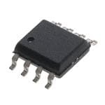
| 描述 | IC EEPROM 4KBIT 2MHZ 8SO电可擦除可编程只读存储器 2.5 V to 5.5V EE |
| 产品分类 | |
| 品牌 | STMicroelectronics |
| 产品手册 | |
| 产品图片 |
|
| rohs | 符合RoHS无铅 / 符合限制有害物质指令(RoHS)规范要求 |
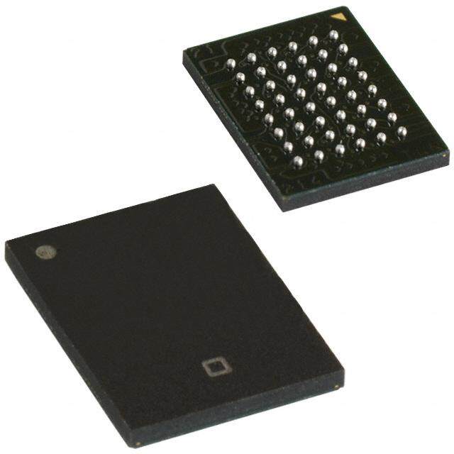
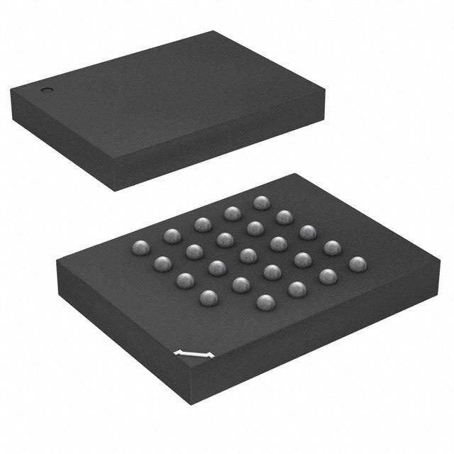
| 产品系列 | 内存,电可擦除可编程只读存储器,STMicroelectronics M93S66-WMN6TP- |
| 数据手册 | |
| 产品型号 | M93S66-WMN6TP |
| 产品目录页面 | |
| 产品种类 | 电可擦除可编程只读存储器 |
| 供应商器件封装 | 8-SO |
| 其它名称 | 497-8668-6 |
| 其它有关文件 | http://www.st.com/web/catalog/mmc/FM76/CL1276/SC112/PF64004?referrer=70071840 |
| 包装 | Digi-Reel® |
| 商标 | STMicroelectronics |
| 存储器类型 | EEPROM |
| 存储容量 | 4 kbit |
| 安装风格 | SMD/SMT |
| 封装 | Reel |
| 封装/外壳 | 8-SOIC(0.154",3.90mm 宽) |
| 封装/箱体 | SOIC-8 Narrow |
| 工作温度 | -40°C ~ 85°C |
| 工作电流 | 2 mA |
| 工作电源电压 | 2.5 V, 5.5 V |
| 工厂包装数量 | 2500 |
| 接口 | Microwire 3 线串行 |
| 接口类型 | Microwire |
| 数据保留 | 40 yr |
| 最大工作温度 | + 85 C |
| 最大工作电流 | 2 mA |
| 最大时钟频率 | 2 MHz |
| 最小工作温度 | - 40 C |
| 标准包装 | 1 |
| 格式-存储器 | EEPROMs - 串行 |
| 电压-电源 | 2.5 V ~ 5.5 V |
| 电源电压-最大 | 5.5 V |
| 电源电压-最小 | 2.5 V |
| 系列 | M93S66-W |
| 组织 | 256 x 16 |
| 速度 | 2MHz |


/IS61LPS102418B-200B3LI.jpg)

- 商务部:美国ITC正式对集成电路等产品启动337调查
- 曝三星4nm工艺存在良率问题 高通将骁龙8 Gen1或转产台积电
- 太阳诱电将投资9.5亿元在常州建新厂生产MLCC 预计2023年完工
- 英特尔发布欧洲新工厂建设计划 深化IDM 2.0 战略
- 台积电先进制程称霸业界 有大客户加持明年业绩稳了
- 达到5530亿美元!SIA预计今年全球半导体销售额将创下新高
- 英特尔拟将自动驾驶子公司Mobileye上市 估值或超500亿美元
- 三星加码芯片和SET,合并消费电子和移动部门,撤换高东真等 CEO
- 三星电子宣布重大人事变动 还合并消费电子和移动部门
- 海关总署:前11个月进口集成电路产品价值2.52万亿元 增长14.8%


_renders/IS43R16800E-5TL.jpg)


PDF Datasheet 数据手册内容提取
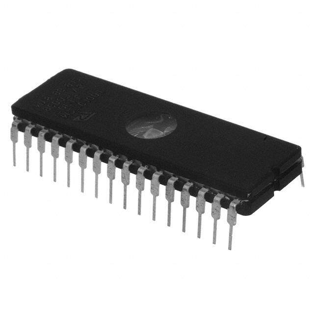
M93S46-W M93S56-W M93S66-W 4 Kbit, 2 Kbit and 1 Kbit serial MICROWIRE bus EEPROM with write protection Datasheet - production data Features • Compatible with MICROWIRE bus serial interface • Memory array − 1 Kbit, 2 Kbit or 4 Kbit of EEPROM − Organized by word (16b) − Page = 4 words • Write PDIP8 (BN) − Byte write within 5 ms − Page write within 5 ms − Ready/busy signal during programming • User defined write protected area • High-speed clock: 2 MHz • Single supply voltage: − 2.5 V to 5.5 V TSSOP8 (DW) • Operating temperature range: 169 mil width • -40 °C up to +85 °C. • Enhanced ESD protection • More than 4 million write cycles • More than 200-year data retention Packages SO8 (MN) • PDIP8 ECOPACK®1 150 mil width • TSSOP8 ECOPACK®2 MSv35377V1 • SO8 ECOPACK®2 January 2015 DocID5124 Rev 7 1/32 This is information on a product in full production www.st.com
Contents M93S46-W M93S56-W M93S66-W Contents 1 Description ........................................................................................ 5 2 Signal description ............................................................................ 6 2.1 Serial data output (Q) ........................................................................ 6 2.2 Serial data input (D) .......................................................................... 6 2.3 Serial clock (C) .................................................................................. 6 2.4 Chip select (S) ................................................................................... 6 2.5 Protection register (PRE) .................................................................. 6 2.6 Write protect (W) ............................................................................... 6 2.7 V ground ........................................................................................ 6 SS 2.8 Supply voltage (V ) ......................................................................... 6 CC 2.8.1 Operating supply voltage V ............................................................. 6 CC 2.8.2 Device reset ........................................................................................ 7 2.8.3 Power-up conditions ........................................................................... 7 2.8.4 Power-down ........................................................................................ 7 3 Operating features ............................................................................ 8 4 Clock pulse counter ......................................................................... 9 5 Instructions ..................................................................................... 10 5.1 Read ............................................................................................... 12 5.2 Write enable and write disable ........................................................ 12 5.3 Write to memory array (WRITE) ...................................................... 13 5.4 Page write ....................................................................................... 14 5.5 Write all ........................................................................................... 15 5.6 Write protection and protect register ............................................... 16 6 Power-up and delivery states ........................................................ 21 6.1 Power-up state ................................................................................ 21 6.2 Initial delivery state .......................................................................... 21 7 Maximum ratings ............................................................................ 22 8 DC and AC parameters .................................................................. 23 9 Package mechanical data .............................................................. 27 10 Part numbering ............................................................................... 30 11 Revision history .............................................................................. 31 2/32 DocID5124 Rev 7
M93S46-W M93S56-W M93S66-W List of tables List of tables Table 1: Signal names ................................................................................................................................ 5 Table 2: Instruction set for the M93S46 .................................................................................................... 10 Table 3: Instruction set for the M93S66, M93S56 .................................................................................... 11 Table 4: Absolute maximum ratings ......................................................................................................... 22 Table 5: Operating conditions (M93Sx6-W) ............................................................................................. 23 Table 6: AC test measurement conditions ................................................................................................ 23 Table 7: Capacitance ................................................................................................................................ 23 Table 8: Memory cell data retention ......................................................................................................... 23 Table 9: Cycling performance ................................................................................................................... 24 Table 10: DC Characteristics (M93Sx6-W, device grade 6) ..................................................................... 24 Table 11: AC Characteristics (M93Sx6-W, device grade 6) ..................................................................... 24 Table 12: SO8N – 8-lead plastic small outline, 150 mils body width, package mechanical data ............. 27 Table 13: PDIP8 – 8 lead plastic dual in-line package, 300 mils body width, package mechanical data 28 Table 14: TSSOP8 - 8-lead thin shrink small outline, package mechanical data ..................................... 29 Table 15: Document revision history ........................................................................................................ 31 DocID5124 Rev 7 3/32
List of figures M93S46-W M93S56-W M93S66-W List of figures Figure 1: Logic diagram .............................................................................................................................. 5 Figure 2: 8-pin package connections .......................................................................................................... 5 Figure 3: Write sequence with one clock glitch .......................................................................................... 9 Figure 4: READ sequence ........................................................................................................................ 12 Figure 5: WRITE sequence ...................................................................................................................... 13 Figure 6: WEN and WDS sequences ....................................................................................................... 13 Figure 7: PAWRITE sequence .................................................................................................................. 15 Figure 8: WRAL sequence ........................................................................................................................ 15 Figure 9: PREAD sequence ...................................................................................................................... 18 Figure 10: PRWRITE sequence ............................................................................................................... 18 Figure 11: PREN sequence ...................................................................................................................... 19 Figure 12: PRCLEAR sequence ............................................................................................................... 19 Figure 13: PRDS sequence ...................................................................................................................... 20 Figure 14: AC test measurement I/O waveform ....................................................................................... 23 Figure 15: Synchronous timing (start and op-code input) ......................................................................... 25 Figure 16: Synchronous timing (read or write) ......................................................................................... 26 Figure 17: Synchronous timing (read or write) ......................................................................................... 26 Figure 18: SO8N – 8-lead plastic small outline 150 mils body width, package outline ............................ 27 Figure 19: PDIP8 – 8-pin plastic DIP, 0.25 mm lead frame, package outline .......................................... 28 Figure 20: TSSOP8 - 8-lead thin shrink small outline, package outline ................................................... 29 Figure 21: Ordering information scheme .................................................................................................. 30 4/32 DocID5124 Rev 7
M93S46-W M93S56-W M93S66-W Description 1 Description The M93S46, M93S56, M93S66 devices are Electrically Erasable PROgrammable Memories (EEPROMs) organized as 64, 128 or 256 words (one word is 16 bits), accessed through the MICROWIRE bus. The M93S46, M93S56, M93S66 can operate with a supply voltage from 2.5 V to 5.5 V over an ambient temperature range of -40 °C / +85 °C. Figure 1: Logic diagram V CC D C Q S M93Sx6 PRE W V SS AI02020B Figure 2: 8-pin package connections M93Sx6 S 1 8 VCC C 2 7 PRE D 3 6 W Q 4 5 VSS AI02021B 1. See Section 9: "Package mechanical data" for package dimensions, and how to identify pin-1. Table 1: Signal names Signal name Function S Chip select input D Serial data input Q Serial data output C Serial clock PRE Protection register enable W Write enable V Supply voltage CC V Ground SS DocID5124 Rev 7 5/32
Signal description M93S46-W M93S56-W M93S66-W 2 Signal description During all operations, V must be held stable and within the specified valid range: CC V (min) to V (max). CC CC All of the input and output signals can be held high or low (according to voltages of V , V , IL IH V or V , as specified in Table 10: "DC Characteristics (M93Sx6-W, device grade 6)". OL OH These signals are described next. 2.1 Serial data output (Q) This output signal is used to transfer data serially out of the device. Data is shifted out on the rising edge of Serial Clock (C). 2.2 Serial data input (D) This input signal is used to transfer data serially into the device. It receives instructions, addresses, and the data to be written. Values are latched on the rising edge of Serial Clock (C). 2.3 Serial clock (C) This input signal provides the timing of the serial interface. Instructions, addresses, or data present at Serial Data Input (D) are latched on the rising edge of Serial Clock (C). Data on Serial Data Output (Q) changes after the rising edge of Serial Clock (C). 2.4 Chip select (S) When this input signal is low, the device is deselected and Serial Data Output (Q) is at high impedance. Unless an internal Write cycle is in progress, the device will be in the Standby Power mode. Driving Chip Select (S) high selects the device, placing it in the Active Power mode. 2.5 Protection register (PRE) The Protection enable (PRE) signal must be driven High before and during the instructions accessing the Protection Register. 2.6 Write protect (W) This input signal is used to control the memory in write protected mode. When Write Protect (W) is held low, writes to the memory are disabled, but other operations remain enabled. Write Protect (W) must either be driven high or low, but must not be left floating. 2.7 V ground SS V is the reference for the V supply voltage. SS CC 2.8 Supply voltage (V ) CC 2.8.1 Operating supply voltage V CC Prior to selecting the memory and issuing instructions to it, a valid and stable VCC voltage within the specified [V (min), V (max)] range must be applied (see Table 5: "Operating CC CC conditions (M93Sx6-W)"). This voltage must remain stable and valid until the end of the 6/32 DocID5124 Rev 7
M93S46-W M93S56-W M93S66-W Signal description transmission of the instruction and, for a Write instruction, until the completion of the internal write cycle (t ). In order to secure a stable DC supply voltage, it is recommended W to decouple the V line with a suitable capacitor (usually of the order of 10 nF to 100 nF) CC close to the V /V package pins. CC SS 2.8.2 Device reset In order to prevent inadvertent write operations during power-up, a power-on-reset (POR) circuit is included. At power-up, the device does not respond to any instruction until V CC reaches the internal reset threshold voltage When V passes over the POR threshold, the device is reset and is in the following state: CC • in Standby Power mode • deselected The device must not be accessed until VCC reaches a valid and stable V voltage within CC the specified [V (min), V (max)] range defined in Table 5: "Operating conditions CC CC (M93Sx6-W)". 2.8.3 Power-up conditions When the power supply is turned on, V must rise continuously from V to V . During CC SS CC this time, the Chip Select (S) line is not allowed to float but should be driven low. It is therefore recommended to connect the S line to V via a suitable pull-down resistor. CC 2.8.4 Power-down During power-down (continuous decrease in the V supply voltage below the minimum CC V operating voltage defined in Table 5: "Operating conditions (M93Sx6-W)", the device CC must be: • deselected (S driven low) • in Standby Power mode (there should not be any internal write cycle in progress). DocID5124 Rev 7 7/32
Operating features M93S46-W M93S56-W M93S66-W 3 Operating features The device is compatible with the MICROWIRE protocol. All instructions, addresses and input data bytes are shifted into the device, most significant bit first. The Serial Data Input (D) is sampled on the first rising edge of the Serial Clock (C) after Chip Select (S) goes high. All output data bytes are shifted out of the device, most significant bit first. The Serial Data Output (Q) is latched on the rising edge of the Serial Clock (C) after the read instruction has been clocked into the device. The M93Sx6 is accessed by a set of instructions which includes Read, Write, Page Write, Write All and instructions used to set the memory protection. These are summarized in Table 2: "Instruction set for the M93S46" and Table 3: "Instruction set for the M93S66, M93S56"). A Read Data from Memory (READ) instruction loads the address of the first word to be read into an internal address counter. The data contained at this address is then clocked out serially. The address counter is automatically incremented after the data is output and, if the Chip Select Input (S) is held High, the M93Sx6 can output a sequential stream of data words. In this way, the memory can be read as a data stream, or continuously as the address counter automatically rolls over to 00h when the highest address is reached. Writing data is internally self-timed (the external clock signal on Serial Clock (C) may be stopped or left running after the start of a Write cycle) and does not require an erase cycle prior to the Write instruction. The Write instruction writes 16 bits at a time into one of the word locations of the M93Sx6, the Page Write instruction writes up to 4 words of 16 bits to sequential locations, assuming in both cases that all addresses are outside the Write Protected area. Up to 4 words may be written with help of the Page Write instruction and the whole memory may also be erased, or written to a predetermined pattern by using the Write All instruction, within the time required by a write cycle (t ). W After the start of the write cycle, a Busy/Ready signal is available on Serial Data Output (Q) when Chip Select Input (S) is driven High. Within the memory, a user defined area may be protected against further Write instructions. The size of this area is defined by the content of a Protection Register, located outside of the memory array. As a final protection step, data in this user defined area may be permanently protected by programming a One Time Programming bit (OTP bit) which locks the Protection Register content. 8/32 DocID5124 Rev 7
M93S46-W M93S56-W M93S66-W Clock pulse counter 4 Clock pulse counter In a noisy environment, the number of pulses received on Serial Clock (C) may be greater than the number delivered by the Bus Master (the micro- controller). This can lead to a misalignment of the instruction of one or more bits (as shown in Figure 3: "Write sequence with one clock glitch".) and may lead to the writing of erroneous data at an erroneous address. To combat this problem, the M93Sx6 has an on-chip counter that counts the clock pulses from the start bit until the falling edge of the Chip Select Input (S). If the number of clock pulses received is not the number expected, the WRITE, PAWRITE, WRALL, PRWRITE or PRCLEAR instruction isaborted, and the contents of the memory are not modified. The number of clock cycles expected for each in- struction, and for each member of the M93Sx6 family, are summarized in Table 2: "Instruction set for the M93S46" and Table 3: "Instruction set for the M93S66, M93S56". For example, a Write Data to Memory (WRITE) instruction on the M93S56 (or M93S66) expects 27 clock cycles from the start bit to the falling edge of Chip Select Input (S). That is: 1 Start bit + 2 Op-code bits + 8 Address bits + 16 Data bits Figure 3: Write sequence with one clock glitch S C D An An-1 An-2 START "0" "1" Glitch D0 ADDRESS AND DATA WRITE ARE SHIFTED BY ONE BIT AI01395B DocID5124 Rev 7 9/32
Instructions M93S46-W M93S56-W M93S66-W 5 Instructions The instruction set of the M93Sx6 devices contains seven instructions, as summarized in Table 2: "Instruction set for the M93S46" and Table 3: "Instruction set for the M93S66, M93S56". Each instruction consists of the following parts, as shown in Figure 4: "READ sequence", Figure 5: "WRITE sequence" and Figure 6: "WEN and WDS sequences": • Each instruction is preceded by a rising edge on Chip Select Input (S) with Serial Clock (C) being held Low. • A start bit, which is the first '1' read on Serial Data Input (D) during the rising edge of Serial Clock (C). • Two op-code bits, read on Serial Data Input (D) during the rising edge of Serial Clock (C). (Some instructions also use the first two bits of the address to define the op-code). • The address bits of the byte or word that is to be accessed. For the M93S46, the address is made up of 6 bits (see Table 2: "Instruction set for the M93S46"). For the M93S56 and M93S66, the address is made up of 8 bits (see Table 3: "Instruction set for the M93S66, M93S56"). The M93Sx6 devices are fabricated in CMOS technology and are therefore able to run as slow as 0 Hz (static input signals) or as fast as the maximum ratings specified in Table 11: "AC Characteristics (M93Sx6-W, device grade 6)". Table 2: Instruction set for the M93S46 Required Start Op- Address Additional Instruction Description W PRE bit code (1) Data clock comments cycles Read Data READ X 0 1 10 A5-A0 Q15-Q0 - - from Memory Write is executed Write Data to if the address is WRITE 1 0 1 01 A5-A0 D15-D0 25 Memory not inside the Protected area Write is executed if all the N Page Write to N x PAWRITE 1 0 1 11 A5-A0 9 + N x 16 addresses are not Memory D15-D0 inside the Protected area Write all data if Write All the Protection WRAL Memory with 1 0 1 00 01 XXXX D15-D0 25 Register is same Data cleared WEN Write Enable 1 0 1 00 11 XXXX - 9 - WDS Write Disable X 0 1 00 00 XXXX - 9 - Data Output = Protection Q5-Q0 Protection PRREAD X 1 1 10 XXXXXX - Register Read + Flag Register content + Protection Flag bit Data above Protection specified address PRWRITE 1 1 1 01 A5-A0 - 9 Register Write A5-A0 are protected 10/32 DocID5124 Rev 7
M93S46-W M93S56-W M93S66-W Instructions Required Start Op- Address Additional Instruction Description W PRE bit code (1) Data clock comments cycles Protect Flag is Protection PRCLEAR 1 1 1 11 111111 - 9 also cleared Register Clear (cleared Flag = 1) Protection PREN Register 1 1 1 00 11XXXX - 9 - Enable Protection OTP bit is set PRDS Register 1 1 1 00 000000 - 9 permanently Disable Note: (1)X = Don’t Care bit. Table 3: Instruction set for the M93S66, M93S56 Required Start Op- Address Additional Instruction Description W PRE bit code (1)(2) Data clock comments cycles Read Data READ X 0 1 10 A7-A0 Q15-Q0 - - from Memory Write is executed if the Write Data to WRITE 1 0 1 01 A7-A0 D15-D0 27 address is not Memory inside the Protected area Write is executed if all Page Write to N x 11 + N x the N addresses PAWRITE 1 0 1 11 A7-A0 Memory D15-D0 16 are not inside the Protected area Write all data if Write All the Protection WRAL Memory with 1 0 1 00 01XXXXXX D15-D0 27 Register is same Data cleared WEN Write Enable 1 0 1 00 11XXXXXX - 11 - WDS Write Disable X 0 1 00 00XXXXXX - 11 - Data Output = Protection Protection Q7-Q0 PRREAD Register X 1 1 10 XXXXXXXX - Register content + Flag Read + Protection Flag bit Data above Protection specified PRWRITE Register 1 1 1 01 A7-A0 - 11 address A7-A0 Write are protected Protect Flag is Protection also cleared PRCLEAR Register 1 1 1 11 11111111 - 11 (cleared Flag = Clear 1) DocID5124 Rev 7 11/32
Instructions M93S46-W M93S56-W M93S66-W Required Start Op- Address Additional Instruction Description W PRE bit code (1)(2) Data clock comments cycles Protection PREN Register 1 1 1 00 11XXXXXX - 11 - Enable Protection OTP bit is set PRDS Register 1 1 1 00 00000000 - 11 permanently Disable Notes: (1)Address bit A7 is not decoded by the M93S56. (2)X = Don’t Care bit. 5.1 Read The Read Data from Memory (READ) instruction outputs serial data on Serial Data Output (Q). When the instruction is received, the op-code and address are decoded, and the data from the memory is transferred to an output shift register. A dummy 0 bit is output first, followed by the 16-bit word, with the most significant bit first. Output data changes are triggered by the rising edge of Serial Clock (C). The M93Sx6 automatically increments the internal address counter and clocks out the next byte (or word) as long as the Chip Select Input (S) is held High. In this case, the dummy 0 bit is not output between bytes (or words) and a continuous stream of data can be read. 5.2 Write enable and write disable The Write Enable (WEN) instruction enables the future execution of write instructions, and the Write Disable (WDS) instruction disables it. When power is first applied, the M93Sx6 initializes itself so that write instructions are disabled. After a Write Enable (WEN) instruction has been executed, writing remains enabled until an Write Disable (WDS) instruction is executed, or until VCC falls below the power-on reset threshold voltage. To protect the memory contents from accidental corruption, it is advisable to issue the Write Disable (WDS) instruction after every write cycle. The Read Data from Memory (READ) instruction is not affected by the Write Enable (WEN) or Write Disable (WDS) instructions. Figure 4: READ sequence READ PRE S D 110An A0 Q Qn Q0 ADDR DATA OUT OP CODE MSv36051V1 12/32 DocID5124 Rev 7
M93S46-W M93S56-W M93S66-W Instructions 1. For the meanings of An and Qn, see Table 2: "Instruction set for the M93S46" and Table 3: "Instruction set for the M93S66, M93S56". Figure 5: WRITE sequence WRITE PRE W S CHECK STATUS D 101An A0Dn D0 Q ADDR DATA IN BUSY READY OP CODE MSv36052V1 1. For the meanings of An and Dn, see Table 2: "Instruction set for the M93S46" and Table 3: "Instruction set for the M93S66, M93S56". Figure 6: WEN and WDS sequences WRITE PRE WRITE PRE ENABLE DISABLE W S S D 10000XnX0 D 10011XnX0 OP CODE OP CODE MSv36053V1 1. For the meanings of Xn, see Table 2: "Instruction set for the M93S46" and Table 3: "Instruction set for the M93S66, M93S56". 5.3 Write to memory array (WRITE) The Write Data to Memory instruction is composed of the Start bit plus the op-code followed by the address and the 16 data bits to be written. Write Enable (W) must be held High before and during the instruction. Input address and data, on Serial Data Input (D) are sampled on the rising edge of Serial Clock (C). DocID5124 Rev 7 13/32
Instructions M93S46-W M93S56-W M93S66-W After the last data bit has been sampled, the Chip Select Input (S) must be taken Low before the next rising edge of Serial Clock (C). If Chip Select Input (S) is brought Low before or after this specific time frame, the self-timed programming cycle will not be started, and the addressed location will not be programmed. While the M93Sx6 is performing a write cycle, but after a delay (t ) before the status SLSH information becomes available, Chip Select Input (S) can be driven High to monitor the status of the write cycle. Serial Data Output (Q) is driven Low while the M93Sx6 is still busy, and High when the cycle is complete, and the M93Sx6 is ready to receive a new instruction. The M93Sx6 ignores any data on the bus while it is busy on a write cycle. Once the M93Sx6 is Ready, Serial Data Output (Q) is driven High, and remains in this state until a new start bit is decoded or the Chip Select Input (S) is brought Low. Programming is internally self-timed, so the external Serial Clock (C) may be disconnected or left running after the start of a write cycle. 5.4 Page write A Page Write to Memory (PAWRITE) instruction contains the first address to be written, followed by up to 4 data words. After the receipt of each data word, bits A1-A0 of the internal address counter are incremented, the high order bits remaining unchanged (A7-A2 for M93S66, M93S56; A5-A2 for M93S46). Users must take care, in the software, to ensure that the last word address has the same upper order address bits as the initial address transmitted to avoid address roll-over. The Page Write to Memory (PAWRITE) instruction will not be executed if any of the 4 words addresses the protected area. Write Enable (W) must be held High before and during the instruction. Input address and data, on Serial Data Input (D) are sampled on the rising edge of Serial Clock (C). After the last data bit has been sampled, the Chip Select Input (S) must be taken Low before the next rising edge of Serial Clock (C). If Chip Select Input (S) is brought Low before or after this specific time frame, the self-timed programming cycle will not be started, and the addressed location will not be programmed. While the M93Sx6 is performing a write cycle, but after a delay (t ) before the status SLSH information becomes available, Chip Select Input (S) can be driven High to monitor the status of the write cycle. Serial Data Output (Q) is driven Low while the M93Sx6 is still busy, and High when the cycle is complete, and the M93Sx6 is ready to receive a new instruction. The M93Sx6 ignores any data on the bus while it is busy on a write cycle. Once the M93Sx6 is Ready, Serial Data Output (Q) is driven High, and remains in this state until a new start bit is decoded or the Chip Select Input (S) is brought Low. Programming is internally self-timed, so the external Serial Clock (C) may be disconnected or left running after the start of a write cycle. 14/32 DocID5124 Rev 7
M93S46-W M93S56-W M93S66-W Instructions Figure 7: PAWRITE sequence PAGE PRE WRITE W S CHECK STATUS D 111An A0Dn D0 Q ADDR DATA IN BUSY READY OP CODE MSv36054V1 1. For the meanings of An and Dn, see Table 2: "Instruction set for the M93S46" and Table 3: "Instruction set for the M93S66, M93S56". 5.5 Write all The Write All Memory with same data (WRAL) instruction is valid only after the Protection Register has been cleared by executing a Protection Register Clear (PRCLEAR) instruction. The Write All Memory with same data (WRAL) instruction simultaneously writes the whole memory with the same data word given in the instruction. Figure 8: WRAL sequence WRITE PRE ALL W S CHECK STATUS D 10001XnX0Dn D0 Q ADDR DATA IN BUSY READY OP CODE MSv36055V1 1. For the meanings of Xn and Dn, see Table 2: "Instruction set for the M93S46" and Table 3: "Instruction set for the M93S66, M93S56". Write Enable (W) must be held High before and during the instruction. Input address and data, on Serial Data Input (D) are sampled on the rising edge of Serial Clock (C). DocID5124 Rev 7 15/32
Instructions M93S46-W M93S56-W M93S66-W After the last data bit has been sampled, the Chip Select Input (S) must be taken Low before the next rising edge of Serial Clock (C). If Chip Select Input (S) is brought Low before or after this specific time frame, the self-timed programming cycle will not be started, and the addressed location will not be programmed. While the M93Sx6 is performing a write cycle, and after a delay (t ) before the status SLSH information becomes available, Chip Select Input (S) can be driven High to monitor the status of the write cycle. Serial Data Output (Q) is driven Low while the M93Sx6 is still busy, and High when the cycle is complete, and the M93Sx6 is ready to receive a new instruction. The M93Sx6 ignores any data on the bus while it is busy on a write cycle. Once the M93Sx6 is Ready, Serial Data Output (Q) is driven High, and remains in this state until a new start bit is decoded or the Chip Select Input (S) is brought Low. Programming is internally self-timed, so the external Serial Clock (C) may be disconnected or left running after the start of a write cycle. 5.6 Write protection and protect register The Protection Register on the M93Sx6 is used to adjust the amount of memory that is to be write protected. The write protected area extends from the address given in the Protection Register, up to the top address in the M93Sx6 device. Two flag bits are used to indicate the Protection Register status: • Protection Flag: this is used to enable/disable protection of the write-protected area of the M93Sx6 memory • OTP bit: when set, this disables access to the Protection Register, and thus prevents any further modifications to the value in the Protection Register. The lower-bound memory address is written to the Protection Register using the Protection Register Write (PRWRITE) instruction. It can be read using the Protection Register Read (PRREAD) instruction. The Protection Register Enable (PREN) instruction must be executed before any PRCLEAR, PRWRITE or PRDS instruction, and with appropriate levels applied to the Protection Enable (PRE) and Write Enable (W) signals. Write-access to the Protection Register is achieved by executing the following sequence: • Execute the Write Enable (WEN) instruction • Execute the Protection Register Enable (PREN) instruction • Execute one PRWRITE, PRCLEAR or PRDS instructions, to set a new boundary address in the Protection Register, to clear the protection address (to all 1s), or permanently to freeze the value held in the Protection Register. Protection register read The Protection Register Read (PRREAD) instruction outputs, on Serial Data Output (Q), the content of the Protection Register, followed by the Protection Flag bit. The Protection Enable (PRE) signal must be driven High before and during the instruction. As with the Read Data from Memory (READ) instruction, a dummy 0 bit is output first. Since it is not possible to distinguish between the Protection Register being cleared (all 1s) or having been written with all 1s, the user must check the Protection Flag status (and not the Protection Register content) to ascertain the setting of the memory protection. Protection register enable The Protection Register Enable (PREN) instruction is used to authorize the use of instructions that modify the Protection Register (PRWRITE, PRCLEAR, PRDS). The 16/32 DocID5124 Rev 7
M93S46-W M93S56-W M93S66-W Instructions Protection Register Enable (PREN) instruction does not modify the Protection Flag bit value. A Write Enable (WEN) instruction must be executed before the Protection Register Enable (PREN) instruction. Both the Protection Enable (PRE) and Write Enable (W) signals must be driven High during the instruction execution. Protection register clear The Protection Register Clear (PRCLEAR) instruction clears the address stored in the Protection Register to all 1s, so that none of the memory is write-protected by the Protection Register. However, it should be noted that all the memory remains protected, in the normal way, using the Write Enable (WEN) and Write Disable (WDS) instructions. The Protection Register Clear (PRCLEAR) instruction clears the Protection Flag to 1. Both the Protection Enable (PRE) and Write Enable (W) signals must be driven High during the instruction execution. A Protection Register Enable (PREN) instruction must immediately precede the Protection Register Clear (PRCLEAR) instruction. Protection register write The Protection Register Write (PRWRITE) instruction is used to write an address into the Protection Register. This is the address of the first word to be protected. After the Protection Register Write (PRWRITE) instruction has been executed, all memory locations equal to and above the specified address are protected from writing. The Protection Flag bit is set to 0, and can be read with Protection Register Read (PRREAD) instruction. Both the Protection Enable (PRE) and Write Enable (W) signals must be driven High during the instruction execution. A Protection Register Enable (PREN) instruction must immediately precede the Protection Register Write (PRWRITE) instruction, but it is not necessary to execute first a Protection Register Clear (PRCLEAR). Protection register disable The Protection Register Disable (PRDS) instruction sets the One Time Programmable (OTP) bit. This instruction is a ONE TIME ONLY instruction which latches the Protection Register content, this content is therefore unalterable in the future. Both the Protection Enable (PRE) and Write Enable (W) signals must be driven High during the instruction execution. The OTP bit cannot be directly read, it can be checked by reading the content of the Protection Register, using the Protection Register Read (PRREAD) instruction, then by writing this same value back into the Protection Register, using the Protection Register Write (PRWRITE) instruction. DocID5124 Rev 7 17/32
Instructions M93S46-W M93S56-W M93S66-W When the OTP bit is set, the Ready/Busy status cannot appear on Serial Data Output (Q). When the OTP bit is not set, the Busy status appears on Serial Data Output (Q). A Protection Register Enable (PREN) instruction must immediately precede the Protection Register Disable (PRDS) instruction. Figure 9: PREAD sequence Protect PRE Register READ S D 110Xn X0 Q An A0F ADDR DATA F = Protect Flag OP OUT CODE MSv36056V1 1. For the meanings of An and Xn, see Table 2: "Instruction set for the M93S46" and Table 3: "Instruction set for the M93S66, M93S56". Figure 10: PRWRITE sequence Protect PRE Register WRITE W S CHECK STATUS D 101An A0 Q ADDR BUSY READY OP CODE MSv36057V1 1. For the meanings of An, see Table 2: "Instruction set for the M93S46" and Table 3: "Instruction set for the M93S66, M93S56". 18/32 DocID5124 Rev 7
M93S46-W M93S56-W M93S66-W Instructions Figure 11: PREN sequence Protect PRE Register ENABLE W S D 10011XnX0 OP CODE MSv36058V1 1. For the meanings of Xn, see Table 2: "Instruction set for the M93S46" and Table 3: "Instruction set for the M93S66, M93S56". Figure 12: PRCLEAR sequence Protect PRE Register CLEAR W S CHECK STATUS D 111 111 Q ADDR BUSY READY OP CODE MSv36059V1 DocID5124 Rev 7 19/32
Instructions M93S46-W M93S56-W M93S66-W Figure 13: PRDS sequence Protect PRE Register DISABLE W S CHECK STATUS D 100 000 Q ADDR BUSY READY OP CODE MSv36060V1 20/32 DocID5124 Rev 7
M93S46-W M93S56-W M93S66-W Power-up and delivery states 6 Power-up and delivery states 6.1 Power-up state After Power-up, the device is in the following state: • low power Standby Power mode • deselected 6.2 Initial delivery state The device is delivered with the memory array set at all 1s (FFh). DocID5124 Rev 7 21/32
Maximum ratings M93S46-W M93S56-W M93S66-W 7 Maximum ratings Stressing the device outside the ratings listed in Table 4: "Absolute maximum ratings" may cause permanent damage to the device. These are stress ratings only, and operation of the device at these, or any other conditions outside those indicated in the operating sections of this specification, is not implied. Exposure to absolute maximum rating conditions for extended periods may affect device reliability. Table 4: Absolute maximum ratings Symbol Parameter Min. Max. Unit T Ambient operating temperature –40 130 °C AMR T Storage temperature –65 150 °C STG T Lead temperature during soldering see note (1) °C LEAD V Output voltage –0.50 V +0.5 V O CC V Input voltage –0.50 V +1.0 V I CC I DC output current (Q = 0) - 5 mA OL I DC output current (Q = 1) - 5 mA OH V Supply voltage –0.50 6.5 V CC V Electrostatic pulse (Human Body Model) voltage (2) - 4000 V ESD Notes: (1) ® Compliant with JEDEC standard J-STD-020D (for small-body, Sn-Pb or Pb assembly), the ST ECOPACK 7191395 specification, and the European directive on Restrictions on Hazardous Substances (RoHS directive 2011/65/EU of July 2011). (2) Positive and negative pulses applied on pin pairs, according to the AEC-Q100-002 (compliant with JEDEC Std JESD22-A114, C1=100 pF, R1=1500 Ω, R2=500 Ω) 22/32 DocID5124 Rev 7
M93S46-W M93S56-W M93S66-W DC and AC parameters 8 DC and AC parameters This section summarizes the operating and measurement conditions, and the DC and AC characteristics of the device. Table 5: Operating conditions (M93Sx6-W) Symbol Parameter Min. Max. Unit V Supply voltage 2.5 5.5 V CC T Ambient operating temperature (device grade 6) –40 85 °C A Table 6: AC test measurement conditions Symbol Parameter Min. Max. Unit CL Load capacitance 100 pF - Input rise and fall times - 50 ns - Input pulse voltages 0.2 VCC to 0.8 VCC V - Input and output timing reference voltages(1) 0.3 VCC to 0.7 VCC V Note: (1)Output Hi-Z is defined as the point where data out is no longer driven. Figure 14: AC test measurement I/O waveform Input and Output Input Levels Timing Reference Levels 0.8 ₓ VCC 0.7 ₓ VCC 0.3 ₓ VCC 0.2 ₓ VCC AI00825C Table 7: Capacitance Symbol Parameter Test condition Min. Max. Unit COUT(1) Output capacitance (Q) V = 0 V - 5 pF OUT CIN(1) Input capacitance V = 0 V - 5 pF IN Note: (1)Sampled only, not 100% tested, at TA= 25 °C. Table 8: Memory cell data retention Parameter Test conditions Min. Unit Data retention (1) TA = 55 °C 200 Year Note: (1) For products identified by process letter K (previous products were specified with a data retention of 40 years at 55 °C) . The data retention behavior is checked in production, while the Min. value (40 years or 200 years) limit is defined from characterization and qualification results. DocID5124 Rev 7 23/32
DC and AC parameters M93S46-W M93S56-W M93S66-W Table 9: Cycling performance Symbol Parameter Test conditions Min. Max. Unit TA ≤ 25 °C, - 4,000,000 V (min) < V < V (max) Ncycle(1) Write cycle endurance CC CC CC Write cycle TA = 85 °C, - 1,200,000 V (min) < V < V (max) CC CC CC Note: (1) Cycling performance for products identified by process letter K (previous products were specified with 1 million cycles at 25 °C). Table 10: DC Characteristics (M93Sx6-W, device grade 6) Symbol Parameter Test condition Min. Max. Unit I Input leakage current 0 V ≤ V ≤ V - ±2.5 µA LI IN CC I Output leakage current 0 V ≤ V ≤ V , Q in Hi-Z - ±2.5 µA LO OUT CC V = 5 V, S = V , f = 1 MHz - 1.5 mA CC IH Supply current VCC = 2.5 V, S = VIH, f = 1 MHz - 1 mA I CC (CMOS inputs) V = 5 V, S = V , f = 2 MHz - 2 mA CC IH V = 2.5 V, S = V , f = 2 MHz - 1 mA CC IH Supply current VCC = 2.5 V, S = VSS, C = VSS - 10 µA I CC1 (stand-by) V = 2.5 V, S = V , C = V - 5 µA CC SS SS Input low voltage V - –0.45 0.2 V V IL CC (D, C, S, PRE, W) Input high voltage V - 0.7 V V + 1 V IH CC CC (D, C, S, PRE, W) V = 5 V, I = 2.1 mA - 0.4 V CC OL V Output low voltage (Q) OL V = 2.5 V, I = 100 µA - 0.2 V CC OL V = 5 V, I = –400 µA 2.4 - V CC OH V Output high voltage (Q) OH V = 2.5 V, I = –100 µA V –0.2 - V CC OH CC Table 11: AC Characteristics (M93Sx6-W, device grade 6) Test conditions specified in Table 5: "Operating conditions (M93Sx6-W)" and Table 6: "AC test measurement conditions" Symbol Alt. Parameter Min. Max. Unit f f Clock frequency D.C. 2 MHz C SK t t Protect enable valid to clock high 50 - ns PRVCH PRES t t Write enable valid to clock high 50 - ns WVCH PES t t Clock low to protect enable transition 0 - ns CLPRX PREH t t Chip select low to write enable transition 250 - ns SLWX PEH t Chip select low to clock high 50 - ns SLCH t t Chip select set-up time 50 - ns SHCH CSS 24/32 DocID5124 Rev 7
M93S46-W M93S56-W M93S66-W DC and AC parameters Test conditions specified in Table 5: "Operating conditions (M93Sx6-W)" and Table 6: "AC test measurement conditions" Symbol Alt. Parameter Min. Max. Unit t (1) t Chip select low to chip select high 200 - ns SLSH CS t (2) t Clock high time 200 - ns CHCL SKH t t Clock low time 200 - ns CLCH SKL t t Data in set-up time 50 - ns DVCH DIS t t Data in hold time 50 - ns CHDX DIH t t Clock set-up time (relative to S) 50 - ns CLSH SKS t t Chip select hold time 0 - ns CLSL CSH t t Chip select to ready/busy status - 200 ns SHQV SV t t Chip Select low to output Hi-Z - 100 ns SLQZ DF t t Delay to output low - 200 ns CHQL PD0 t t Delay to output valid - 200 ns CHQV PD1 t t Erase/Write cycle time - 5 ms W WP Notes: (1)Chip Select Input (S) must be brought Low for a minimum of tSLSH between consecutive instruction cycles. (2)tCHCL + tCLCH ≥ 1 / fC. Figure 15: Synchronous timing (start and op-code input) PRE tPRVCH W tWVCH tCHCL C tCLSH tSHCH tCLCH S tDVCH tCHDX D START OP CODE OP CODE OP CODE INPUT START AI02025B DocID5124 Rev 7 25/32
DC and AC parameters M93S46-W M93S56-W M93S66-W Figure 16: Synchronous timing (read or write) C tCLSL S tDVCH tCHDX tCHQV tSLSH D An A0 tCHQL tSLQZ Hi-Z Q Q15 Q0 ADDRESS INPUT DATA OUTPUT AI02026B Figure 17: Synchronous timing (read or write) PRE tCLPRX W tSLWX C tSLCH tCLSL S tSLSH tDVCH tCHDX D An A0/D0 tSHQV tSLQZ Hi-Z Q BUSY READY tW ADDRESS/DATA INPUT WRITE CYCLE AI02027B 26/32 DocID5124 Rev 7
M93S46-W M93S56-W M93S66-W Package mechanical data 9 Package mechanical data In order to meet environmental requirements, ST offers the device in different grades of ECOPACK® packages, depending on their level of environmental compliance. ECOPACK® specifications, grade definitions and product status are available at: www.st.com. ECOPACK® is an ST trademark. Figure 18: SO8N – 8-lead plastic small outline 150 mils body width, package outline h x 45˚ A2 A c ccc b e 0.25 mm D GAUGE PLANE k 8 E1 E 1 A1 L L1 SO-A_V2 1. Drawing is not to scale. Table 12: SO8N – 8-lead plastic small outline, 150 mils body width, package mechanical data millimeters inches (1) Symbol Typ Min Max Typ Min Max A - - 1.75 - - 0.0689 A1 - 0.1 0.25 - 0.0039 0.0098 A2 - 1.25 - - 0.0492 - b - 0.28 0.48 - 0.011 0.0189 c - 0.17 0.23 - 0.0067 0.0091 ccc - - 0.1 - - 0.0039 D 4.9 4.8 5 0.1929 0.189 0.1969 E 6 5.8 6.2 0.2362 0.2283 0.2441 E1 3.9 3.8 4 0.1535 0.1496 0.1575 e 1.27 - - 0.05 - - h - 0.25 0.5 - 0.0098 0.0197 k - 0° 8° - 0° 8° L - 0.4 1.27 - 0.0157 0.05 L1 1.04 - - 0.0409 - - Note: (1)Values in inches are converted from mm and rounded to 4 decimal digits. DocID5124 Rev 7 27/32
Package mechanical data M93S46-W M93S56-W M93S66-W Figure 19: PDIP8 – 8-pin plastic DIP, 0.25 mm lead frame, package outline E b2 A2 A A1 L b e c eA eB D 8 E1 1 PDIP-B_V2 1. Drawing is not to scale. 2. Not recommended for new designs. Table 13: PDIP8 – 8 lead plastic dual in-line package, 300 mils body width, package mechanical data millimeters inches (1) Symbol Typ. Min. Max. Typ. Min. Max. A - - 5.33 - - 0.2098 A1 - 0.38 - - 0.015 - A2 3.3 2.92 4.95 0.1299 0.115 0.1949 b 0.46 0.36 0.56 0.0181 0.0142 0.022 b2 1.52 1.14 1.78 0.0598 0.0449 0.0701 c 0.25 0.2 0.36 0.0098 0.0079 0.0142 D 9.27 9.02 10.16 0.365 0.3551 0.4 E 7.87 7.62 8.26 0.3098 0.3 0.3252 E1 6.35 6.1 7.11 0.25 0.2402 0.2799 e 2.54 - - 0.1 - - eA 7.62 - - 0.3 - - eB - - 10.92 - - 0.4299 L 3.3 2.92 3.81 0.1299 0.115 0.15 Note: (1)Values in inches are converted from mm and rounded to 4 decimal digits. 28/32 DocID5124 Rev 7
M93S46-W M93S56-W M93S66-W Package mechanical data Figure 20: TSSOP8 - 8-lead thin shrink small outline, package outline D 8 5 c E1 E 1 4 α A1 L A A2 CP L1 b e TSSOP8AM_V2 1. Drawing is not to scale. Table 14: TSSOP8 - 8-lead thin shrink small outline, package mechanical data millimeters inches (1) Symbol Typ Min Max Typ Min Max A - - 1.2 - - 0.0472 A1 - 0.05 0.15 - 0.002 0.0059 A2 1 0.8 1.05 0.0394 0.0315 0.0413 b - 0.19 0.3 - 0.0075 0.0118 c - 0.09 0.2 - 0.0035 0.0079 CP - - 0.1 - - 0.0039 D 3 2.9 3.1 0.1181 0.1142 0.122 e 0.65 - - 0.0256 - - E 6.4 6.2 6.6 0.252 0.2441 0.2598 E1 4.4 4.3 4.5 0.1732 0.1693 0.1772 L 0.6 0.45 0.75 0.0236 0.0177 0.0295 L1 1 - - 0.0394 - - α - 0° 8° - 0° 8° N (number of leads) 8 8 Note: (1)Values in inches are converted from mm and rounded to 4 decimal digits. DocID5124 Rev 7 29/32
Part numbering M93S46-W M93S56-W M93S66-W 10 Part numbering Figure 21: Ordering information scheme Example: M93S66 - W MN 6 T P Device Type M93 = MICROWIRE serial access EEPROM (x16) with Block Protection Device Function 66 = 4 Kbit (256 x 16) 56 = 2 Kbit (128 x 16) 46 = 1 Kbit (64 x 16) Operating Voltage W = VCC = 2.5 to 5.5 V Package BN = PDIP8 MN = SO8 (150 mil width) DW = TSSOP8 (169 mil width) Device Grade 6 = Industrial: device tested with standard test flow over –40 to 85 °C Option blank = Standard Packing T = Tape & Reel Packing Plating Technology P or G = ECOPACK® (RoHS compliant) MSv36049V1 Engineering samples Parts marked as “ES”, “E” or accompanied by an Engineering Sample notification letter, are not yet qualified and therefore not yet ready to be used in production and any consequences deriving from such usage will not be at ST charge. In no event, ST will be liable for any customer usage of these engineering samples in production. ST Quality has to be contacted prior to any decision to use these engineering samples to run qualification activity. 30/32 DocID5124 Rev 7
M93S46-W M93S56-W M93S66-W Revision history 11 Revision history Table 15: Document revision history Date Revision Changes Document reformatted, and reworded, using the new template. Temperature range 1 removed. TSSOP8 (3x3mm) package added. New 07-Mar-2002 2.0 products, identified by the process letter W, added, with fc(max) increased to 1MHz for -R voltage range, and to 2MHz for all other ranges (and corresponding parameters adjusted). Value of standby current (max) corrected in DC characteristics tables for 26-Mar-2003 2.1 -W and -R ranges V and V separated from V in the Absolute OUT IN IO Maximum Ratings table. Values corrected in AC characteristics tables for -W range (tSLSH, 14-Apr-2003 2.2 tDVCH, tCLSL) for devices with Process Identification Letter W. Standby current corrected for -R range. Four missing parameters 23-May-2003 2.3 restored to all AC Characteristics tables. Table of contents, and Pb-free options added. V (min) improved to - 24-Nov-2003 3.0 IL 0.45V. Absolute Maximum Ratings for V (min) and V (min) changed. IO CC Soldering temperature information clarified for RoHS compliant devices. 19-Apr-2004 4.0 Device Grade 3 clarified, with reference to HRCF and automotive environments. Process identification letter “G” information added. Document reformatted. 13-Mar-2013 5 Modified the part number names and the content of the entire document. Updated Features on page 1. Updated note under Table 4: "Absolute maximum ratings". 25-Nov-2013 6 Added Table 8: "Memory cell data retention". Added Table 9: "Cycling performance". Removed sentence after Table 1: "Signal names". Updated Table 8: "Memory cell data retention" footnote (1). Updated Table 9: "Cycling performance" footnote (1). 08-Jan-2015 7 Added footnote to Table 13: "PDIP8 – 8 lead plastic dual in-line package, 300 mils body width, package mechanical data". Added engineering samples information in Section 10: "Part numbering". DocID5124 Rev 7 31/32
M93S46-W M93S56-W M93S66-W IMPORTANT NOTICE – PLEASE READ CAREFULLY STMicroelectronics NV and its subsidiaries (“ST”) reserve the right to make changes, corrections, enhancements, modifications, and improvements to ST products and/or to this document at any time without notice. Purchasers should obtain the latest relevant information on ST products before placing orders. ST products are sold pursuant to ST’s terms and conditions of sale in place at the time of order acknowledgement. Purchasers are solely responsible for the choice, selection, and use of ST products and ST assumes no liability for application assistance or the design of Purchasers’ products. No license, express or implied, to any intellectual property right is granted by ST herein. Resale of ST products with provisions different from the information set forth herein shall void any warranty granted by ST for such product. ST and the ST logo are trademarks of ST. All other product or service names are the property of their respective owners. Information in this document supersedes and replaces information previously supplied in any prior versions of this document. © 2015 STMicroelectronics – All rights reserved 32/32 DocID5124 Rev 7
Mouser Electronics Authorized Distributor Click to View Pricing, Inventory, Delivery & Lifecycle Information: S TMicroelectronics: M93S46-WMN6P M93S66-WMN6P M93S46-WMN6TP M93S56-WMN6P M93S56-WMN6TP M93S66-WMN6TP