 Datasheet下载
- 型号: M28W320FCB70ZB6E
- 制造商: Micron Technology Inc
- 库位|库存: xxxx|xxxx
- 要求:
| 数量阶梯 | 香港交货 | 国内含税 |
| +xxxx | $xxxx | ¥xxxx |
查看当月历史价格
查看今年历史价格
M28W320FCB70ZB6E产品简介:
ICGOO电子元器件商城为您提供M28W320FCB70ZB6E由Micron Technology Inc设计生产,在icgoo商城现货销售,并且可以通过原厂、代理商等渠道进行代购。 M28W320FCB70ZB6E价格参考。Micron Technology IncM28W320FCB70ZB6E封装/规格:存储器, FLASH - NOR 存储器 IC 32Mb (2M x 16) 并联 70ns 47-TFBGA(6.39x6.37)。您可以下载M28W320FCB70ZB6E参考资料、Datasheet数据手册功能说明书,资料中有M28W320FCB70ZB6E 详细功能的应用电路图电压和使用方法及教程。
| 参数 | 数值 |
| 产品目录 | 集成电路 (IC) |
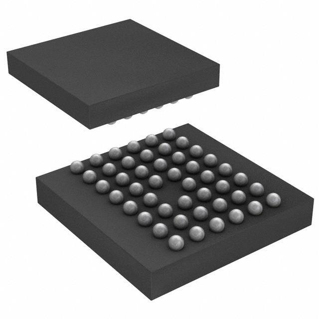
| 描述 | IC FLASH 32MBIT 70NS 47TFBGA |
| 产品分类 | |
| 品牌 | Micron Technology Inc |
| 数据手册 | |
| 产品图片 |
|
| 产品型号 | M28W320FCB70ZB6E |
| rohs | 无铅 / 符合限制有害物质指令(RoHS)规范要求 |
| 产品系列 | - |
| 产品目录页面 | |
| 供应商器件封装 | 47-TFBGA(6.39x6.37) |
| 包装 | 托盘 |
| 存储器类型 | FLASH - NOR |
| 存储容量 | 32M(2M x 16) |
| 封装/外壳 | 47-TFBGA |
| 工作温度 | -40°C ~ 85°C |
| 接口 | 并联 |
| 标准包装 | 1,380 |
| 格式-存储器 | 闪存 |
| 电压-电源 | 2.7 V ~ 3.6 V |
| 速度 | 70ns |


- 商务部:美国ITC正式对集成电路等产品启动337调查
- 曝三星4nm工艺存在良率问题 高通将骁龙8 Gen1或转产台积电
- 太阳诱电将投资9.5亿元在常州建新厂生产MLCC 预计2023年完工
- 英特尔发布欧洲新工厂建设计划 深化IDM 2.0 战略
- 台积电先进制程称霸业界 有大客户加持明年业绩稳了
- 达到5530亿美元!SIA预计今年全球半导体销售额将创下新高
- 英特尔拟将自动驾驶子公司Mobileye上市 估值或超500亿美元
- 三星加码芯片和SET,合并消费电子和移动部门,撤换高东真等 CEO
- 三星电子宣布重大人事变动 还合并消费电子和移动部门
- 海关总署:前11个月进口集成电路产品价值2.52万亿元 增长14.8%


PDF Datasheet 数据手册内容提取
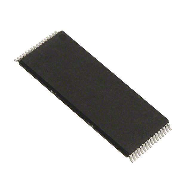
M28W320FCT M28W320FCB 32 Mbit (2Mb x16, Boot Block) 3V Supply Flash Memory Features (cid:132) Supply Voltage – V = 2.7V to 3.6V Core Power Supply FBGA DD – V = 1.65V to 3.6V for Input/Output DDQ – V = 12V for fast Program (optional) PP TFBGA47 (ZB) 6.39 x 6.37mm (cid:132) Access Time: 70, 80, 90, 100ns (cid:132) Programming Time – 10μs typical – Double Word Programming Option – Quadruple Word Programming Option (cid:132) Common Flash Interface (cid:132) Memory Blocks TSOP48 (N) – Parameter Blocks (Top or Bottom location) 12 x 20mm – Main Blocks (cid:132) Block Locking – All blocks locked at Power Up – Any combination of blocks can be locked – WP for Block Lock-Down (cid:132) Security – 128 bit user Programmable OTP cells – 64 bit unique device identifier (cid:132) Automatic Stand-by mode (cid:132) Program and Erase Suspend (cid:132) 100,000 Program/Erase cycles per block (cid:132) Electronic Signature – Manufacturer Code: 20h – Top Device Code, M28W320FCT: 88BAh – Bottom Device Code, M28W320FCB: 88BBh (cid:132) RoHS compliant packages November 2008 208010-05 1/69 www.numonyx.com 1
Contents M28W320FCT, M28W320FCB Contents 1 Summary description . . . . . . . . . . . . . . . . . . . . . . . . . . . . . . . . . . . . . . . . 7 2 Signal descriptions . . . . . . . . . . . . . . . . . . . . . . . . . . . . . . . . . . . . . . . . . 12 2.1 Address inputs (A0-A20) . . . . . . . . . . . . . . . . . . . . . . . . . . . . . . . . . . . . . 12 2.2 Data input/output (DQ0-DQ15) . . . . . . . . . . . . . . . . . . . . . . . . . . . . . . . . . 12 2.3 Chip Enable (E) . . . . . . . . . . . . . . . . . . . . . . . . . . . . . . . . . . . . . . . . . . . . 12 2.4 Output Enable (G) . . . . . . . . . . . . . . . . . . . . . . . . . . . . . . . . . . . . . . . . . . 12 2.5 Write Enable (W) . . . . . . . . . . . . . . . . . . . . . . . . . . . . . . . . . . . . . . . . . . . 12 2.6 Write Protect (WP) . . . . . . . . . . . . . . . . . . . . . . . . . . . . . . . . . . . . . . . . . . 12 2.7 Reset (RP) . . . . . . . . . . . . . . . . . . . . . . . . . . . . . . . . . . . . . . . . . . . . . . . . 13 2.8 V supply voltage . . . . . . . . . . . . . . . . . . . . . . . . . . . . . . . . . . . . . . . . . . 13 DD 2.9 V supply voltage . . . . . . . . . . . . . . . . . . . . . . . . . . . . . . . . . . . . . . . . . 13 DDQ 2.10 V Program supply voltage . . . . . . . . . . . . . . . . . . . . . . . . . . . . . . . . . . 13 PP 2.11 V ground . . . . . . . . . . . . . . . . . . . . . . . . . . . . . . . . . . . . . . . . . . . . . . . . 13 SS 3 Bus operations . . . . . . . . . . . . . . . . . . . . . . . . . . . . . . . . . . . . . . . . . . . . 14 3.1 Read . . . . . . . . . . . . . . . . . . . . . . . . . . . . . . . . . . . . . . . . . . . . . . . . . . . . . 14 3.2 Write . . . . . . . . . . . . . . . . . . . . . . . . . . . . . . . . . . . . . . . . . . . . . . . . . . . . . 14 3.3 Output Disable . . . . . . . . . . . . . . . . . . . . . . . . . . . . . . . . . . . . . . . . . . . . . 14 3.4 Standby . . . . . . . . . . . . . . . . . . . . . . . . . . . . . . . . . . . . . . . . . . . . . . . . . . 14 3.5 Automatic Standby . . . . . . . . . . . . . . . . . . . . . . . . . . . . . . . . . . . . . . . . . . 15 3.6 Reset . . . . . . . . . . . . . . . . . . . . . . . . . . . . . . . . . . . . . . . . . . . . . . . . . . . . 15 4 Command interface . . . . . . . . . . . . . . . . . . . . . . . . . . . . . . . . . . . . . . . . . 16 4.1 Read Memory Array command . . . . . . . . . . . . . . . . . . . . . . . . . . . . . . . . 16 4.2 Read Status Register command . . . . . . . . . . . . . . . . . . . . . . . . . . . . . . . . 16 4.3 Read Electronic Signature command . . . . . . . . . . . . . . . . . . . . . . . . . . . . 17 4.4 Read CFI Query command . . . . . . . . . . . . . . . . . . . . . . . . . . . . . . . . . . . 17 4.5 Block Erase command . . . . . . . . . . . . . . . . . . . . . . . . . . . . . . . . . . . . . . . 18 4.6 Program command . . . . . . . . . . . . . . . . . . . . . . . . . . . . . . . . . . . . . . . . . . 18 4.7 Double Word Program command . . . . . . . . . . . . . . . . . . . . . . . . . . . . . . . 19 4.8 Quadruple Word Program command . . . . . . . . . . . . . . . . . . . . . . . . . . . . 19 2/69
M28W320FCT, M28W320FCB Contents 4.9 Clear Status Register command . . . . . . . . . . . . . . . . . . . . . . . . . . . . . . . . 19 4.10 Program/Erase Suspend command . . . . . . . . . . . . . . . . . . . . . . . . . . . . . 20 4.11 Program/Erase Resume command . . . . . . . . . . . . . . . . . . . . . . . . . . . . . 20 4.12 Protection Register Program command . . . . . . . . . . . . . . . . . . . . . . . . . . 20 4.13 Block Lock command . . . . . . . . . . . . . . . . . . . . . . . . . . . . . . . . . . . . . . . . 21 4.14 Block Unlock command . . . . . . . . . . . . . . . . . . . . . . . . . . . . . . . . . . . . . . 21 4.15 Block Lock-Down command . . . . . . . . . . . . . . . . . . . . . . . . . . . . . . . . . . . 21 5 Block locking . . . . . . . . . . . . . . . . . . . . . . . . . . . . . . . . . . . . . . . . . . . . . . 25 5.1 Reading a Block’s Lock Status . . . . . . . . . . . . . . . . . . . . . . . . . . . . . . . . . 25 5.2 Locked state . . . . . . . . . . . . . . . . . . . . . . . . . . . . . . . . . . . . . . . . . . . . . . . 25 5.3 Unlocked state . . . . . . . . . . . . . . . . . . . . . . . . . . . . . . . . . . . . . . . . . . . . . 25 5.4 Lock-Down state . . . . . . . . . . . . . . . . . . . . . . . . . . . . . . . . . . . . . . . . . . . . 26 5.5 Locking operations during Erase Suspend . . . . . . . . . . . . . . . . . . . . . . . . 26 6 Status Register . . . . . . . . . . . . . . . . . . . . . . . . . . . . . . . . . . . . . . . . . . . . 28 6.1 Program/Erase Controller Status (Bit 7) . . . . . . . . . . . . . . . . . . . . . . . . . . 28 6.2 Erase Suspend Status (Bit 6) . . . . . . . . . . . . . . . . . . . . . . . . . . . . . . . . . . 28 6.3 Erase Status (Bit 5) . . . . . . . . . . . . . . . . . . . . . . . . . . . . . . . . . . . . . . . . . 29 6.4 Program Status (Bit 4) . . . . . . . . . . . . . . . . . . . . . . . . . . . . . . . . . . . . . . . 29 6.5 V Status (Bit 3) . . . . . . . . . . . . . . . . . . . . . . . . . . . . . . . . . . . . . . . . . . . 29 PP 6.6 Program Suspend Status (Bit 2) . . . . . . . . . . . . . . . . . . . . . . . . . . . . . . . . 29 6.7 Block Protection Status (Bit 1) . . . . . . . . . . . . . . . . . . . . . . . . . . . . . . . . . 30 6.8 Reserved (Bit 0) . . . . . . . . . . . . . . . . . . . . . . . . . . . . . . . . . . . . . . . . . . . . 30 7 Maximum rating . . . . . . . . . . . . . . . . . . . . . . . . . . . . . . . . . . . . . . . . . . . . 31 8 DC and AC parameters . . . . . . . . . . . . . . . . . . . . . . . . . . . . . . . . . . . . . . 32 9 Package mechanical . . . . . . . . . . . . . . . . . . . . . . . . . . . . . . . . . . . . . . . . 41 10 Part numbering . . . . . . . . . . . . . . . . . . . . . . . . . . . . . . . . . . . . . . . . . . . . 44 Appendix A Block address tables. . . . . . . . . . . . . . . . . . . . . . . . . . . . . . . . . . . . . 46 Appendix B Common Flash Interface (CFI) . . . . . . . . . . . . . . . . . . . . . . . . . . . . . 51 3/69
Contents M28W320FCT, M28W320FCB Appendix C Flowcharts and pseudo codes . . . . . . . . . . . . . . . . . . . . . . . . . . . . . 56 Appendix D Command interface and Program/Erase Controller state . . . . . . . 64 11 Revision history . . . . . . . . . . . . . . . . . . . . . . . . . . . . . . . . . . . . . . . . . . . 68 4/69
M28W320FCT, M28W320FCB List of tables List of tables Table 1. Signal Names. . . . . . . . . . . . . . . . . . . . . . . . . . . . . . . . . . . . . . . . . . . . . . . . . . . . . . . . . . . . 8 Table 2. Bus Operations. . . . . . . . . . . . . . . . . . . . . . . . . . . . . . . . . . . . . . . . . . . . . . . . . . . . . . . . . . 15 Table 3. Command Codes . . . . . . . . . . . . . . . . . . . . . . . . . . . . . . . . . . . . . . . . . . . . . . . . . . . . . . . . 17 Table 4. Commands. . . . . . . . . . . . . . . . . . . . . . . . . . . . . . . . . . . . . . . . . . . . . . . . . . . . . . . . . . . . . 22 Table 5. Read Electronic Signature . . . . . . . . . . . . . . . . . . . . . . . . . . . . . . . . . . . . . . . . . . . . . . . . . 23 Table 6. Read Block Lock Signature . . . . . . . . . . . . . . . . . . . . . . . . . . . . . . . . . . . . . . . . . . . . . . . . 23 Table 7. Read Protection Register and Lock Register . . . . . . . . . . . . . . . . . . . . . . . . . . . . . . . . . . . 23 Table 8. Program, Erase Times and Program/Erase Endurance Cycles . . . . . . . . . . . . . . . . . . . . . 24 Table 9. Block Lock Status. . . . . . . . . . . . . . . . . . . . . . . . . . . . . . . . . . . . . . . . . . . . . . . . . . . . . . . . 26 Table 10. Protection Status . . . . . . . . . . . . . . . . . . . . . . . . . . . . . . . . . . . . . . . . . . . . . . . . . . . . . . . . 27 Table 11. Status Register Bits . . . . . . . . . . . . . . . . . . . . . . . . . . . . . . . . . . . . . . . . . . . . . . . . . . . . . . 30 Table 12. Absolute Maximum Ratings . . . . . . . . . . . . . . . . . . . . . . . . . . . . . . . . . . . . . . . . . . . . . . . . 31 Table 13. Operating and AC Measurement Conditions . . . . . . . . . . . . . . . . . . . . . . . . . . . . . . . . . . . 32 Table 14. Capacitance . . . . . . . . . . . . . . . . . . . . . . . . . . . . . . . . . . . . . . . . . . . . . . . . . . . . . . . . . . . . 33 Table 15. DC Characteristics . . . . . . . . . . . . . . . . . . . . . . . . . . . . . . . . . . . . . . . . . . . . . . . . . . . . . . . 33 Table 16. Read AC Characteristics . . . . . . . . . . . . . . . . . . . . . . . . . . . . . . . . . . . . . . . . . . . . . . . . . . 35 Table 17. Write AC Characteristics, Write Enable Controlled. . . . . . . . . . . . . . . . . . . . . . . . . . . . . . . 37 Table 18. Write AC Characteristics, Chip Enable Controlled . . . . . . . . . . . . . . . . . . . . . . . . . . . . . . . 39 Table 19. Power-Up and Reset AC Characteristics . . . . . . . . . . . . . . . . . . . . . . . . . . . . . . . . . . . . . . 40 Table 20. TSOP48 - 48 lead Plastic Thin Small Outline, 12 x 20mm, Package Mechanical Data . . . 41 Table 21. TFBGA47 6.39x6.37mm - 8x6 ball array, 0.75mm pitch, Package Mechanical Data. . . . . 42 Table 22. Ordering Information Scheme. . . . . . . . . . . . . . . . . . . . . . . . . . . . . . . . . . . . . . . . . . . . . . . 44 Table 23. Daisy Chain Ordering Scheme. . . . . . . . . . . . . . . . . . . . . . . . . . . . . . . . . . . . . . . . . . . . . . 45 Table 24. Top Boot Block Addresses, M28W320FCT . . . . . . . . . . . . . . . . . . . . . . . . . . . . . . . . . . . . 46 Table 25. Bottom Boot Block Addresses, M28W320FCB. . . . . . . . . . . . . . . . . . . . . . . . . . . . . . . . . . 48 Table 26. Query Structure Overview . . . . . . . . . . . . . . . . . . . . . . . . . . . . . . . . . . . . . . . . . . . . . . . . . 51 Table 27. CFI Query Identification String . . . . . . . . . . . . . . . . . . . . . . . . . . . . . . . . . . . . . . . . . . . . . . 51 Table 28. CFI Query System Interface Information . . . . . . . . . . . . . . . . . . . . . . . . . . . . . . . . . . . . . . 52 Table 29. Device Geometry Definition. . . . . . . . . . . . . . . . . . . . . . . . . . . . . . . . . . . . . . . . . . . . . . . . 53 Table 30. Primary Algorithm-Specific Extended Query Table. . . . . . . . . . . . . . . . . . . . . . . . . . . . . . . 54 Table 31. Security Code Area. . . . . . . . . . . . . . . . . . . . . . . . . . . . . . . . . . . . . . . . . . . . . . . . . . . . . . . 55 Table 32. Write State Machine Current/Next, sheet 1 of 2. . . . . . . . . . . . . . . . . . . . . . . . . . . . . . . . . 64 Table 33. Write State Machine Current/Next, sheet 2 of 2 . . . . . . . . . . . . . . . . . . . . . . . . . . . . . . . . 66 Table 34. Document revision history . . . . . . . . . . . . . . . . . . . . . . . . . . . . . . . . . . . . . . . . . . . . . . . . . 68 5/69
List of figures M28W320FCT, M28W320FCB List of figures Figure 1. Logic Diagram. . . . . . . . . . . . . . . . . . . . . . . . . . . . . . . . . . . . . . . . . . . . . . . . . . . . . . . . . . . . 8 Figure 2. TSOP Connections. . . . . . . . . . . . . . . . . . . . . . . . . . . . . . . . . . . . . . . . . . . . . . . . . . . . . . . . 9 Figure 3. TFBGA Connections (Top view through package). . . . . . . . . . . . . . . . . . . . . . . . . . . . . . . 10 Figure 4. Block Addresses. . . . . . . . . . . . . . . . . . . . . . . . . . . . . . . . . . . . . . . . . . . . . . . . . . . . . . . . . 11 Figure 5. Protection Register Memory Map. . . . . . . . . . . . . . . . . . . . . . . . . . . . . . . . . . . . . . . . . . . . 11 Figure 6. AC Measurement I/O Waveform. . . . . . . . . . . . . . . . . . . . . . . . . . . . . . . . . . . . . . . . . . . . . 32 Figure 7. AC Measurement Load Circuit . . . . . . . . . . . . . . . . . . . . . . . . . . . . . . . . . . . . . . . . . . . . . . 33 Figure 8. Read AC Waveforms . . . . . . . . . . . . . . . . . . . . . . . . . . . . . . . . . . . . . . . . . . . . . . . . . . . . . 35 Figure 9. Write AC Waveforms, Write Enable Controlled . . . . . . . . . . . . . . . . . . . . . . . . . . . . . . . . . 36 Figure 10. Write AC Waveforms, Chip Enable Controlled. . . . . . . . . . . . . . . . . . . . . . . . . . . . . . . . . . 38 Figure 11. Power-Up and Reset AC Waveforms. . . . . . . . . . . . . . . . . . . . . . . . . . . . . . . . . . . . . . . . . 40 Figure 12. TSOP48 - 48 lead Plastic Thin Small Outline, 12 x 20mm, Package Outline. . . . . . . . . . . 41 Figure 13. TFBGA47 6.39x6.37mm - 8x6 ball array, 0.75mm pitch, Bottom View Package Outline. . 42 Figure 14. TFBGA47 Daisy Chain - Package Connections (Top view through package) . . . . . . . . . . 43 Figure 15. TFBGA47 Daisy Chain - PCB Connections proposal (Top view through package) . . . . . . 43 Figure 16. Program Flowchart and Pseudo Code . . . . . . . . . . . . . . . . . . . . . . . . . . . . . . . . . . . . . . . . 56 Figure 17. Double Word Program Flowchart and Pseudo Code . . . . . . . . . . . . . . . . . . . . . . . . . . . . . 57 Figure 18. Quadruple Word Program Flowchart and Pseudo Code . . . . . . . . . . . . . . . . . . . . . . . . . . 58 Figure 19. Program Suspend & Resume Flowchart and Pseudo Code. . . . . . . . . . . . . . . . . . . . . . . . 59 Figure 20. Erase Flowchart and Pseudo Code . . . . . . . . . . . . . . . . . . . . . . . . . . . . . . . . . . . . . . . . . . 60 Figure 21. Erase Suspend & Resume Flowchart and Pseudo Code. . . . . . . . . . . . . . . . . . . . . . . . . . 61 Figure 22. Locking Operations Flowchart and Pseudo Code . . . . . . . . . . . . . . . . . . . . . . . . . . . . . . . 62 Figure 23. Protection Register Program Flowchart and Pseudo Code . . . . . . . . . . . . . . . . . . . . . . . . 63 6/69
M28W320FCT, M28W320FCB Summary description 1 Summary description The M28W320FCT and M28W320FCB are 32 Mbit (2 Mbit x 16) non-volatile Flash memories that can be erased electrically at the block level and programmed in-system on a Word-by-Word basis. These operations can be performed using a single low voltage (2.7 to 3.6V) supply. V allows to drive the I/O pin down to 1.65V. An optional 12V V power DDQ PP supply is provided to speed up customer programming. The devices feature an asymmetrical blocked architecture. They have an array of 71 blocks: 8 Parameter Blocks of 4 KWord and 63 Main Blocks of 32 KWord. M28W320FCT has the Parameter Blocks at the top of the memory address space while the M28W320FCB locates the Parameter Blocks starting from the bottom. The memory maps are shown in Figure4: Block Addresses. Both devices feature an instant, individual block locking scheme that allows any block to be locked or unlocked with no latency, enabling instant code and data protection. All blocks have three levels of protection. They can be locked and locked-down individually preventing any accidental programming or erasure. There is an additional hardware protection against program and erase. When V ≤ V all blocks are protected against program or erase. PP PPLK All blocks are locked at Power Up. Each block can be erased separately. Erase can be suspended in order to perform either read or program in any other block and then resumed. Program can be suspended to read data in any other block and then resumed. Each block can be programmed and erased over 100,000 cycles. The device includes a Protection Register to increase the protection of a system design. The Protection Register is divided into two segments, the first is a 64 bit area which contains a unique device number written by Numonyx, while the second is a 128 bit area, one-time- programmable by the user. The user programmable segment can be permanently protected. Figure5, shows the Protection Register Memory Map. Program and Erase commands are written to the Command Interface of the memory. An on- chip Program/Erase Controller takes care of the timings necessary for program and erase operations. The end of a program or erase operation can be detected and any error conditions identified. The command set required to control the memory is consistent with JEDEC standards. The memory is offered in TSOP48 (10 X 20mm) and TFBGA47 (6.39 x 6.37mm, 0.75mm pitch) packages and is supplied with all the bits erased (set to ’1’). In order to meet environmental requirements, Numonyx offers the M28W320FCT and M28W320FCB in RoHS compliant packages. RoHS compliant packages are Lead-free. The category of second Level Interconnect is marked on the package and on the inner box label, in compliance with JEDEC Standard JESD97. The maximum ratings related to soldering conditions are also marked on the inner box label. 7/69
Summary description M28W320FCT, M28W320FCB Figure 1. Logic Diagram VDD VDDQ VPP 21 16 A0-A20 DQ0-DQ15 W E M28W320FCT M28W320FCB G RP WP VSS AI09900 T able 1. Signal Names A0-A20 Address Inputs DQ0-DQ15 Data Input/Output E Chip Enable G Output Enable W Write Enable RP Reset WP Write Protect V Core Power Supply DD V Power Supply for Input/Output DDQ V Optional Supply Voltage for Fast Program & Erase PP V Ground SS NC Not Connected Internally 8/69
M28W320FCT, M28W320FCB Summary description Figure 2. TSOP Connections A15 1 48 A16 A14 VDDQ A13 VSS A12 DQ15 A11 DQ7 A10 DQ14 A9 DQ6 A8 DQ13 NC DQ5 A20 DQ12 W DQ4 RP 12 M28W320FCT 37 VDD VPP 13 M28W320FCB 36 DQ11 WP DQ3 A19 DQ10 A18 DQ2 A17 DQ9 A7 DQ1 A6 DQ8 A5 DQ0 A4 G A3 VSSQ A2 E A1 24 25 A0 AI09901b 9/69
Summary description M28W320FCT, M28W320FCB Figure 3. TFBGA Connections (Top view through package) 1 2 3 4 5 6 7 8 A A13 A11 A8 VPP WP A19 A7 A4 B A14 A10 W RP A18 A17 A5 A2 C A15 A12 A9 A20 A6 A3 A1 D A16 DQ14 DQ5 DQ11 DQ2 DQ8 E A0 E VDDQ DQ15 DQ6 DQ12 DQ3 DQ9 DQ0 VSSQ F VSS DQ7 DQ13 DQ4 VDD DQ10 DQ1 G AI03847b 10/69
M28W320FCT, M28W320FCB Summary description Figure 4. Block Addresses M28W320FCT M28W320FCB Top Boot Block Addresses Bottom Boot Block Addresses 1FFFFF 1FFFFF 4 KWords 32 KWords 1FF000 1F8000 1F7FFF 32 KWords Total of 8 4 KWord Blocks 1F0000 Total of 63 1F8FFF 32 KWord Bloc 4 KWords 1F8000 1F7FFF 32 KWords 1F0000 00FFFF 32 KWords 008000 007FFF 4 KWords Total of 63 007000 32 KWord Blocks 00FFFF Total of 8 32 KWords 4 KWord Block 008000 007FFF 000FFF 32 KWords 4 KWords 000000 000000 AI09902 1. Also see Appendix A, Table24 and Table25 for a full listing of the Block Addresses. Figure 5. Protection Register Memory Map PROTECTION REGISTER 8Ch User Programmable OTP 85h 84h Unique device number 81h 80h Protection Register Lock 2(1) 1 0 Note1. Bit 2 of the Protection Register Lock must not be programmed to 0. AI05520 11/69
Signal descriptions M28W320FCT, M28W320FCB 2 Signal descriptions See Figure1: Logic Diagram and Table1: Signal Names, for a brief overview of the signals connected to this device. 2.1 Address inputs (A0-A20) The Address Inputs select the cells in the memory array to access during Bus Read operations. During Bus Write operations they control the commands sent to the Command Interface of the internal state machine. 2.2 Data input/output (DQ0-DQ15) The Data I/O outputs the data stored at the selected address during a Bus Read operation or inputs a command or the data to be programmed during a Write Bus operation. 2.3 Chip Enable (E) The Chip Enable input activates the memory control logic, input buffers, decoders and sense amplifiers. When Chip Enable is at V andReset is at V the device is in active IL IH mode. When Chip Enable is at V the memory is deselected, the outputs are high IH impedance and the power consumption is reduced to the stand-by level. 2.4 Output Enable (G) The Output Enable controls data outputs during the Bus Read operation of the memory. 2.5 Write Enable (W) The Write Enable controls the Bus Write operation of the memory’s Command Interface. The data and address inputs are latched on the rising edge of Chip Enable, E, or Write Enable, W, whichever occurs first. 2.6 Write Protect (WP) Write Protect is an input that gives an additional hardware protection for each block. When Write Protect is at V , the Lock-Down is enabled and the protection status of the block IL cannot be changed. When Write Protect is at V , the Lock-Down is disabled and the block IH can be locked or unlocked. (refer to Table7: Read Protection Register and Lock Register). 12/69
M28W320FCT, M28W320FCB Signal descriptions 2.7 Reset (RP) The Reset input provides a hardware reset of the memory. When Reset is at V , the IL memory is in reset mode: the outputs are high impedance and the current consumption is minimized. After Reset all blocks are in the Locked state. When Reset is at V , the device is IH in normal operation. Exiting reset mode the device enters read array mode, but a negative transition of Chip Enable or a change of the address is required to ensure valid data outputs. 2.8 V supply voltage DD V provides the power supply to the internal core of the memory device. It is the main DD power supply for all operations (Read, Program and Erase). 2.9 V supply voltage DDQ V provides the power supply to the I/O pins and enables all Outputs to be powered DDQ independently from V . V can be tied to V or can use a separate supply. DD DDQ DD 2.10 V Program supply voltage PP V is both a control input and a power supply pin. The two functions are selected by the PP voltage range applied to the pin. The Supply Voltage V and the Program Supply Voltage DD V can be applied in any order. PP If V is kept in a low voltage range (0V to 3.6V) V is seen as a control input. In this case PP PP a voltage lower than V gives an absolute protection against program or erase, while PPLK V > V enables these functions (see Table15: DC Characteristics). V is only PP PP1 PP sampled at the beginning of a Program or Erase; a change in its value after the operation has started does not have any effect on Program or Erase, however for Double or Quadruple Word Program the results are uncertain. If V is in the range 11.4V to 12.6V it acts as a power supply pin. In this condition V must PP PP be stable until the Program/Erase algorithm is completed (see Table17 and Table18). 2.11 V ground SS V is the reference for all voltage measurements. SS Note: Each device in a system should have V ,V and V decoupled with a 0.1μF DD DDQ PP capacitor close to the pin. See Figure7: AC Measurement Load Circuit. The PCB trace widths should be sufficient to carry the required V program and erase currents. PP 13/69
Bus operations M28W320FCT, M28W320FCB 3 Bus operations There are six standard bus operations that control the device. These are Bus Read, Bus Write, Output Disable, Standby, Automatic Standby and Reset. See Table2: Bus Operations, for a summary. Typically glitches of less than 5ns on Chip Enable or Write Enable are ignored by the memory and do not affect bus operations. 3.1 Read Read Bus operations are used to output the contents of the Memory Array, the Electronic Signature, the Status Register and the Common Flash Interface. Both Chip Enable and Output Enable must be at V in order to perform a read operation. The Chip Enable input IL should be used to enable the device. Output Enable should be used to gate data onto the output. The data read depends on the previous command written to the memory (see Command Interface section). See Figure8: Read AC Waveforms, and Table16: Read AC Characteristics, for details of when the output becomes valid. Read mode is the default state of the device when exiting Reset or after power-up. 3.2 Write Bus Write operations write Commands to the memory or latch Input Data to be programmed. A write operation is initiated when Chip Enable and Write Enable are at V IL with Output Enable at V . Commands, Input Data and Addresses are latched on the rising IH edge of Write Enable or Chip Enable, whichever occurs first. See Figure9 and Figure10, Write AC Waveforms, and Table17 and Table18, Write AC Characteristics, for details of the timing requirements. 3.3 Output Disable The data outputs are high impedance when the Output Enable is at V . IH 3.4 Standby Standby disables most of the internal circuitry allowing a substantial reduction of the current consumption. The memory is in stand-by when Chip Enable is at V and the device is in IH read mode. The power consumption is reduced to the stand-by level and the outputs are set to high impedance, independently from the Output Enable or Write Enable inputs. If Chip Enable switches to V during a program or erase operation, the device enters Standby IH mode when finished. 14/69
M28W320FCT, M28W320FCB Bus operations 3.5 Automatic Standby Automatic Standby provides a low power consumption state during Read mode. Following a read operation, the device enters Automatic Standby after 150ns of bus inactivity even if Chip Enable is Low, V , and the supply current is reduced to I . The data Inputs/Outputs IL DD1 will still output data if a bus Read operation is in progress. 3.6 Reset During Reset mode when Output Enable is Low, V , the memory is deselected and the IL outputs are high impedance. The memory is in Reset mode when Reset is at V . The power IL consumption is reduced to the Standby level, independently from the Chip Enable, Output Enable or Write Enable inputs. If Reset is pulled to V during a Program or Erase, this SS operation is aborted and the memory content is no longer valid. Table 2. B us Operations(1) Operation E G W RP WP V DQ0-DQ15 PP Bus Read V V V V X Don't Care Data Output IL IL IH IH Bus Write V V V V X V or V Data Input IL IH IL IH DD PPH Output Disable V V V V X Don't Care Hi-Z IL IH IH IH Standby V X X V X Don't Care Hi-Z IH IH Reset X X X V X Don't Care Hi-Z IL 1. X = V or V , V = 12V ± 5%. IL IH PPH 15/69
Command interface M28W320FCT, M28W320FCB 4 Command interface All Bus Write operations to the memory are interpreted by the Command Interface. Commands consist of one or more sequential Bus Write operations. An internal Program/Erase Controller handles all timings and verifies the correct execution of the Program and Erase commands. The Program/Erase Controller provides a Status Register whose output may be read at any time during, to monitor the progress of the operation, or the Program/Erase states. See Table3: Command Codes, for a summary of the commands and see Appendix D, and Table32, Write State Machine Current/Next, for a summary of the Command Interface. The Command Interface is reset to Read mode when power is first applied, when exiting from Reset or whenever V is lower than V . Command sequences must be followed DD LKO exactly. Any invalid combination of commands will reset the device to Read mode. Refer to Table4: Commands, in conjunction with the text descriptions below. 4.1 Read Memory Array command The Read command returns the memory to its Read mode. One Bus Write cycle is required to issue the Read Memory Array command and return the memory to Read mode. Subsequent read operations will read the addressed location and output the data. When a device Reset occurs, the memory defaults to Read mode. 4.2 Read Status Register command The Status Register indicates when a program or erase operation is complete and the success or failure of the operation itself. Issue a Read Status Register command to read the Status Register’s contents. Subsequent Bus Read operations read the Status Register at any address, until another command is issued. See Table11: Status Register Bits, for details on the definitions of the bits. The Read Status Register command may be issued at any time, even during a Program/Erase operation. Any Read attempt during a Program/Erase operation will automatically output the content of the Status Register. 16/69
M28W320FCT, M28W320FCB Command interface 4.3 Read Electronic Signature command The Read Electronic Signature command reads the Manufacturer and Device Codes and the Block Locking Status, or the Protection Register. The Read Electronic Signature command consists of one write cycle, a subsequent read will output the Manufacturer Code, the Device Code, the Block Lock and Lock-Down Status, or the Protection and Lock Register. See Table5, Table6 and Table7 for the valid address. T able 3. Command Codes Hex Code Command 01h Block Lock confirm 10h Program 20h Erase 2Fh Block Lock-Down confirm 30h Double Word Program 40h Program 50h Clear Status Register 55h Reserved 56h Quadruple Word Program 60h Block Lock, Block Unlock, Block Lock-Down 70h Read Status Register 90h Read Electronic Signature 98h Read CFI Query B0h Program/Erase Suspend C0h Protection Register Program D0h Program/Erase Resume, Block Unlock confirm FFh Read Memory Array 4.4 Read CFI Query command The Read Query Command is used to read data from the Common Flash Interface (CFI) Memory Area, allowing programming equipment or applications to automatically match their interface to the characteristics of the device. One Bus Write cycle is required to issue the Read Query Command. Once the command is issued subsequent Bus Read operations read from the Common Flash Interface Memory Area. See Appendix B: Common Flash Interface (CFI), Table26, Table27, Table28, Table29, Table30 and Table31 for details on the information contained in the Common Flash Interface memory area. 17/69
Command interface M28W320FCT, M28W320FCB 4.5 Block Erase command The Block Erase command can be used to erase a block. It sets all the bits within the selected block to ’1’. All previous data in the block is lost. If the block is protected then the Erase operation will abort, the data in the block will not be changed and the Status Register will output the error. Two Bus Write cycles are required to issue the command. 1. The first bus cycle sets up the Erase command. 2. The second latches the block address in the internal state machine and starts the Program/Erase Controller. If the second bus cycle is not Write Erase Confirm (D0h), Status Register bits b4 and b5 are set and the command aborts. Erase aborts if Reset turns to V . As data integrity cannot be guaranteed when the Erase IL operation is aborted, the block must be erased again. During Erase operations the memory will accept the Read Status Register command and the Program/Erase Suspend command, all other commands will be ignored. Typical Erase times are given in Table8: Program, Erase Times and Program/Erase Endurance Cycles. See Appendix C, Figure20: Erase Flowchart and Pseudo Code, for a suggested flowchart for using the Erase command. 4.6 Program command The memory array can be programmed word-by-word. Two bus write cycles are required to issue the Program Command. 1. The first bus cycle sets up the Program command. 2. The second latches the Address and the Data to be written and starts the Program/Erase Controller. During Program operations the memory will accept the Read Status Register command and the Program/Erase Suspend command. Typical Program times are given in Table8: Program, Erase Times and Program/Erase Endurance Cycles. Programming aborts if Reset goes to V . As data integrity cannot be guaranteed when the IL program operation is aborted, the block containing the memory location must be erased and reprogrammed. See Appendix C, Figure16: Program Flowchart and Pseudo Code, for the flowchart for using the Program command. 18/69
M28W320FCT, M28W320FCB Command interface 4.7 Double Word Program command This feature is offered to improve the programming throughput, writing a page of two adjacent words in parallel.The two words must differ only for the address A0. Programming should not be attempted when V is not at V . PP PPH Three bus write cycles are necessary to issue the Double Word Program command. 1. The first bus cycle sets up the Double Word Program Command. 2. The second bus cycle latches the Address and the Data of the first word to be written. 3. The third bus cycle latches the Address and the Data of the second word to be written and starts the Program/Erase Controller. Read operations output the Status Register content after the programming has started. Programming aborts if Reset goes to V . As data integrity cannot be guaranteed when the IL program operation is aborted, the block containing the memory location must be erased and reprogrammed. See Appendix C, Figure17: Double Word Program Flowchart and Pseudo Code, for the flowchart for using the Double Word Program command. 4.8 Quadruple Word Program command This feature is offered to improve the programming throughput, writing a page of four adjacent words in parallel.The four words must differ only for the addresses A0 and A1. Programming should not be attempted when V is not at V . PP PPH Five bus write cycles are necessary to issue the Quadruple Word Program command. 1. The first bus cycle sets up the Quadruple Word Program Command. 2. The second bus cycle latches the Address and the Data of the first word to be written. 3. The third bus cycle latches the Address and the Data of the second word to be written. 4. The fourth bus cycle latches the Address and the Data of the third word to be written. 5. The fifth bus cycle latches the Address and the Data of the fourth word to be written and starts the Program/Erase Controller. Read operations output the Status Register content after the programming has started. Programming aborts if Reset goes to V . As data integrity cannot be guaranteed when the IL program operation is aborted, the block containing the memory location must be erased and reprogrammed. See Appendix C, Figure18: Quadruple Word Program Flowchart and Pseudo Code, for the flowchart for using the Quadruple Word Program command. 4.9 Clear Status Register command The Clear Status Register command can be used to reset bits 1, 3, 4 and 5 in the Status Register to ‘0’. One bus write cycle is required to issue the Clear Status Register command. The bits in the Status Register do not automatically return to ‘0’ when a new Program or Erase command is issued. The error bits in the Status Register should be cleared before attempting a new Program or Erase command. 19/69
Command interface M28W320FCT, M28W320FCB 4.10 Program/Erase Suspend command The Program/Erase Suspend command is used to pause a Program or Erase operation. One bus write cycle is required to issue the Program/Erase command and pause the Program/Erase controller. During Program/Erase Suspend the Command Interface will accept the Program/Erase Resume, Read Array, Read Status Register, Read Electronic Signature and Read CFI Query commands. Additionally, if the suspend operation was Erase then the Program, Double Word Program, Quadruple Word Program, Block Lock, Block Lock-Down or Protection Program commands will also be accepted. The block being erased may be protected by issuing the Block Protect, Block Lock or Protection Program commands. When the Program/Erase Resume command is issued the operation will complete. Only the blocks not being erased may be read or programmed correctly. During a Program/Erase Suspend, the device can be placed in a pseudo-standby mode by taking Chip Enable to V . Program/Erase is aborted if Reset turns to V . IH IL See Appendix C, Figure19: Program Suspend & Resume Flowchart and Pseudo Code, and Figure21: Erase Suspend & Resume Flowchart and Pseudo Code for flowcharts for using the Program/Erase Suspend command. 4.11 Program/Erase Resume command The Program/Erase Resume command can be used to restart the Program/Erase Controller after a Program/Erase Suspend operation has paused it. One Bus Write cycle is required to issue the command. Once the command is issued subsequent Bus Read operations read the Status Register. See Appendix C, Figure19: Program Suspend & Resume Flowchart and Pseudo Code, and Figure21: Erase Suspend & Resume Flowchart and Pseudo Code, and Figure21: Erase Suspend & Resume Flowchart and Pseudo Code for flowcharts for using the Program/Erase Resume command. 4.12 Protection Register Program command The Protection Register Program command is used to Program the 128 bit user One-Time- Programmable (OTP) segment of the Protection Register. The segment is programmed 16 bits at a time. When shipped all bits in the segment are set to ‘1’. The user can only program the bits to ‘0’. Two write cycles are required to issue the Protection Register Program command. 1. The first bus cycle sets up the Protection Register Program command. 2. The second latches the Address and the Data to be written to the Protection Register and starts the Program/Erase Controller. Read operations output the Status Register content after the programming has started. The segment can be protected by programming bit 1 of the Protection Lock Register (see Figure5: Protection Register Memory Map). Attempting to program a previously protected Protection Register will result in a Status Register error. The protection of the Protection Register is not reversible. The Protection Register Program cannot be suspended. 20/69
M28W320FCT, M28W320FCB Command interface 4.13 Block Lock command The Block Lock command is used to lock a block and prevent Program or Erase operations from changing the data in it. All blocks are locked at power-up or reset. Two Bus Write cycles are required to issue the Block Lock command. 1. The first bus cycle sets up the Block Lock command. 2. The second Bus Write cycle latches the block address. The lock status can be monitored for each block using the Read Electronic Signature command. Table10 shows the protection status after issuing a Block Lock command. The Block Lock bits are volatile, once set they remain set until a hardware reset or power- down/power-up. They are cleared by a Blocks Unlock command. Refer to the section, Block Locking, for a detailed explanation. 4.14 Block Unlock command The Block Unlock command is used to unlock a block, allowing the block to be programmed or erased. Two Bus Write cycles are required to issue the Block Unlock command. 1. The first bus cycle sets up the Block Unlock command. 2. The second Bus Write cycle latches the block address. The lock status can be monitored for each block using the Read Electronic Signature command. Table10 shows the protection status after issuing a Block Unlock command. Refer to the section, Block Locking, for a detailed explanation. 4.15 Block Lock-Down command A locked block cannot be Programmed or Erased, or have its protection status changed when WP is low, V . When WP is high, V the Lock-Down function is disabled and the IL IH, locked blocks can be individually unlocked by the Block Unlock command. Two Bus Write cycles are required to issue the Block Lock-Down command. 1. The first bus cycle sets up the Block Lock command. 2. The second Bus Write cycle latches the block address. The lock status can be monitored for each block using the Read Electronic Signature command. Locked-Down blocks revert to the locked (and not locked-down) state when the device is reset on power-down. Table10 shows the protection status after issuing a Block Lock-Down command. Refer to the section, Block Locking, for a detailed explanation. 21/69
Command interface M28W320FCT, M28W320FCB Table 4. C ommands(1)(2) Bus Write Operations s e Commands cl 1st Cycle 2nd Cycle 3rd Cycle 4th Cycle 5th Cycle y C Op Add Data Op Add Data Op Add Data Op Add Data Op Add Data Read Memory 1+ Write X FFh Read RA RD Array Read Status 1+ Write X 70h Read X SRD Register Read Electronic SA 1+ Write X 90h Read IDh Signature (3) Read CFI Query 1+ Write X 98h Read QA QD Erase 2 Write X 20h Write BA D0h 40h Program 2 Write X or Write PA PD 10h Double Word 3 Write X 30h Write PA1 PD1 Write PA2 PD2 Program(4) Quadruple Word 56h 5 Write X Write PA1 PD1 Write PA2 PD2 Write PA3 PD3 Write PA4 PD4 Program(5) (6) Clear Status 1 Write X 50h Register Program/Erase 1 Write X B0h Suspend Program/Erase 1 Write X D0h Resume Block Lock 2 Write X 60h Write BA 01h Block Unlock 2 Write X 60h Write BA D0h Block Lock-Down 2 Write X 60h Write BA 2Fh Protection 2 Write X C0h Write PRA PRD Register Program 1. X = Don't Care, RA=Read Address, RD=Read Data, SRD=Status Register Data, ID=Identifier (Manufacture and Device Code), QA=Query Address, QD=Query Data, BA=Block Address, PA=Program Address, PD=Program Data, PRA=Protection Register Address, PRD=Protection Register Data. 2. 55h is reserved. 3. The signature addresses are listed in Table5, Table6 and Table7. 4. Program Addresses 1 and 2 must be consecutive Addresses differing only for A0. 5. Program Addresses 1,2,3 and 4 must be consecutive Addresses differing only for A0 and A1. 6. To be characterized. 22/69
M28W320FCT, M28W320FCB Command interface Table 5. R ead Electronic Signature(1) Code Device E G W A0 A1 A2-A7 A8-A20 DQ0-DQ7 DQ8-DQ15 Manufacture. V V V V V 0 Don't Care 20h 00h Code IL IL IH IL IL M28W320FCT V V V V V 0 Don't Care BAh 88h IL IL IH IH IL Device Code M28W320FCB V V V V V 0 Don't Care BBh 88h IL IL IH IH IL 1. RP = V . IH Table 6. R ead Block Lock Signature Block Status E G W A0 A1 A2-A7 A8-A11 A12-A20 DQ0 DQ1 DQ2-DQ15 Locked Block V V V V V 0 Don't Care Block Address 1 0 00h IL IL IH IL IH Unlocked Block V V V V V 0 Don't Care Block Address 0 0 00h IL IL IH IL IH Locked-Down V V V V V 0 Don't Care Block Address X(1) 1 00h Block IL IL IH IL IH 1. A Locked-Down Block can be locked "DQ0 = 1" or unlocked "DQ0 = 0"; see Block Locking section. Table 7. R ead Protection Register and Lock Register A0- DQ3- DQ8- Word E G W A8-A20 DQ0 DQ1 DQ2 A7 DQ7 DQ15 OTP Prot. Don't Care Don't Lock V V V 80h Don't Care Don't Care Don't Care IL IL IH data See note(1) Care Unique ID 0 V V V 81h Don't Care ID data ID data ID data ID data ID data IL IL IH Unique ID 1 V V V 82h Don't Care ID data ID data ID data ID data ID data IL IL IH Unique ID 2 V V V 83h Don't Care ID data ID data ID data ID data ID data IL IL IH Unique ID 3 V V V 84h Don't Care ID data ID data ID data ID data ID data IL IL IH OTP OTP 0 V V V 85h Don't Care OTP data OTP data OTP data OTP data IL IL IH data OTP OTP 1 V V V 86h Don't Care OTP data OTP data OTP data OTP data IL IL IH data OTP OTP 2 V V V 87h Don't Care OTP data OTP data OTP data OTP data IL IL IH data OTP OTP 3 V V V 88h Don't Care OTP data OTP data OTP data OTP data IL IL IH data OTP OTP 4 V V V 89h Don't Care OTP data OTP data OTP data OTP data IL IL IH data OTP OTP 5 V V V 8Ah Don't Care OTP data OTP data OTP data OTP data IL IL IH data OTP OTP 6 V V V 8Bh Don't Care OTP data OTP data OTP data OTP data IL IL IH data OTP OTP 7 V V V 8Ch Don't Care OTP data OTP data OTP data OTP data IL IL IH data 1. DQ2 in the Protection Lock Register must not be programmed to 0. 23/69
Command interface M28W320FCT, M28W320FCB Table 8. P rogram, Erase Times and Program/Erase Endurance Cycles M28W320FCT, M28W320FCB Parameter Test Conditions Unit Min Typ Max Word Program V = V 10 200 μs PP DD Double Word Program V = 12V ±5% 10 200 μs PP Quadruple Word Program V = 12V ±5% 10 200 μs PP V = 12V ±5% 0.16/0.08 (1) 5 s PP Main Block Program V = V 0.32 5 s PP DD V = 12V ±5% 0.02/0.01(1) 4 s PP Parameter Block Program V = V 0.04 4 s PP DD V = 12V ±5% 1 10 s PP Main Block Erase V = V 1 10 s PP DD V = 12V ±5% 0.4 10 s PP Parameter Block Erase V = V 0.4 10 s PP DD Program/Erase Cycles (per Block) 100,000 cycles Data Retention 20 years 1. Typical time to program a Main or Parameter Block using the Double Word Program and the Quadruple Word Program commands respectively. 24/69
M28W320FCT, M28W320FCB Block locking 5 Block locking The M28W320FCT and M28W320FCB feature an instant, individual block locking scheme that allows any block to be locked or unlocked with no latency. This locking scheme has three levels of protection. (cid:132) Lock/Unlock - this first level allows software-only control of block locking. (cid:132) Lock-Down - this second level requires hardware interaction before locking can be changed. (cid:132) V ≤ V - the third level offers a complete hardware protection against program PP PPLK and erase on all blocks. The protection status of each block can be set to Locked, Unlocked, and Lock-Down. Table10 defines all of the possible protection states (WP, DQ1, DQ0), and Appendix C, Figure22, shows a flowchart for the locking operations. 5.1 Reading a Block’s Lock Status The lock status of every block can be read in the Read Electronic Signature mode of the device. To enter this mode write 90h to the device. Subsequent reads at the address specified in Table6, will output the protection status of that block. The lock status is represented by DQ0 and DQ1. DQ0 indicates the Block Lock/Unlock status and is set by the Lock command and cleared by the Unlock command. It is also automatically set when entering Lock-Down. DQ1 indicates the Lock-Down status and is set by the Lock-Down command. It cannot be cleared by software, only by a hardware reset or power-down. The following sections explain the operation of the locking system. 5.2 Locked state The default status of all blocks on power-up or after a hardware reset is Locked (states (0,0,1) or (1,0,1)). Locked blocks are fully protected from any program or erase. Any program or erase operations attempted on a locked block will return an error in the Status Register. The Status of a Locked block can be changed to Unlocked or Lock-Down using the appropriate software commands. An Unlocked block can be Locked by issuing the Lock command. 5.3 Unlocked state Unlocked blocks (states (0,0,0), (1,0,0) (1,1,0)), can be programmed or erased. All unlocked blocks return to the Locked state after a hardware reset or when the device is powered- down. The status of an unlocked block can be changed to Locked or Locked-Down using the appropriate software commands. A locked block can be unlocked by issuing the Unlock command. 25/69
Block locking M28W320FCT, M28W320FCB 5.4 Lock-Down state Blocks that are Locked-Down (state (0,1,x))are protected from program and erase operations (as for Locked blocks) but their protection status cannot be changed using software commands alone. A Locked or Unlocked block can be Locked-Down by issuing the Lock-Down command. Locked-Down blocks revert to the Locked state when the device is reset or powered-down. The Lock-Down function is dependent on the WP input pin. When WP=0 (V ), the blocks in IL the Lock-Down state (0,1,x) are protected from program, erase and protection status changes. When WP=1 (V ) the Lock-Down function is disabled (1,1,1) and Locked-Down IH blocks can be individually unlocked to the (1,1,0) state by issuing the software command, where they can be erased and programmed. These blocks can then be locked again (1,1,1) and unlocked (1,1,0) as desired while WP remains high. When WP is low, blocks that were previously Locked-Down return to the Lock-Down state (0,1,x) regardless of any changes made while WP was high. Device reset or power-down resets all blocks, including those in Lock-Down, to the Locked state. 5.5 Locking operations during Erase Suspend Changes to block lock status can be performed during an erase suspend by using the standard locking command sequences to unlock, lock or lock-down a block. This is useful in the case when another block needs to be updated while an erase operation is in progress. To change block locking during an erase operation, first write the Erase Suspend command, then check the status register until it indicates that the erase operation has been suspended. Next write the desired Lock command sequence to a block and the lock status will be changed. After completing any desired lock, read, or program operations, resume the erase operation with the Erase Resume command. If a block is locked or locked-down during an erase suspend of the same block, the locking status bits will be changed immediately, but when the erase is resumed, the erase operation will complete. Locking operations cannot be performed during a program suspend. Refer to Appendix D: Command interface and Program/Erase Controller state, for detailed information on which commands are valid during erase suspend. T able 9. Block Lock Status Item Address Data Block Lock Configuration LOCK Block is Unlocked DQ0=0 xx002 Block is Locked DQ0=1 Block is Locked-Down DQ1=1 26/69
M28W320FCT, M28W320FCB Block locking Table 10. Protection Status Current Protection Status(1) Next Protection Status(1) (WP, DQ1, DQ0) (WP, DQ1, DQ0) After After After Block Program/Erase After Current State Block Lock Block Unlock Lock-Down Allowed WP transition Command Command Command 1,0,0 yes 1,0,1 1,0,0 1,1,1 0,0,0 1,0,1(2) no 1,0,1 1,0,0 1,1,1 0,0,1 1,1,0 yes 1,1,1 1,1,0 1,1,1 0,1,1 1,1,1 no 1,1,1 1,1,0 1,1,1 0,1,1 0,0,0 yes 0,0,1 0,0,0 0,1,1 1,0,0 0,0,1(2) no 0,0,1 0,0,0 0,1,1 1,0,1 0,1,1 no 0,1,1 0,1,1 0,1,1 1,1,1 or 1,1,0 (3) 1. The lock status is defined by the write protect pin and by DQ1 (‘1’ for a locked-down block) and DQ0 (‘1’ for a locked block) as read in the Read Electronic Signature command with A1 = V and A0 = V . IH IL 2. All blocks are locked at power-up, so the default configuration is 001 or 101 according to WP status. 3. A WP transition to V on a locked block will restore the previous DQ0 value, giving a 111 or 110. IH 27/69
Status Register M28W320FCT, M28W320FCB 6 Status Register The Status Register provides information on the current or previous Program or Erase operation. The various bits convey information and errors on the operation. To read the Status register the Read Status Register command can be issued, refer to Read Status Register Command section. To output the contents, the Status Register is latched on the falling edge of the Chip Enable or Output Enable signals, and can be read until Chip Enable or Output Enable returns to V . Either Chip Enable or Output Enable must be toggled to IH update the latched data. Bus Read operations from any address always read the Status Register during Program and Erase operations. The bits in the Status Register are summarized in Table11: Status Register Bits. Refer to Table11 in conjunction with the following text descriptions. 6.1 Program/Erase Controller Status (Bit 7) The Program/Erase Controller Status bit indicates whether the Program/Erase Controller is active or inactive. When the Program/Erase Controller Status bit is Low (set to ‘0’), the Program/Erase Controller is active; when the bit is High (set to ‘1’), the Program/Erase Controller is inactive, and the device is ready to process a new command. The Program/Erase Controller Status is Low immediately after a Program/Erase Suspend command is issued until the Program/Erase Controller pauses. After the Program/Erase Controller pauses the bit is High. During Program, Erase, operations the Program/Erase Controller Status bit can be polled to find the end of the operation. Other bits in the Status Register should not be tested until the Program/Erase Controller completes the operation and the bit is High. After the Program/Erase Controller completes its operation the Erase Status, Program Status, V Status and Block Lock Status bits should be tested for errors. PP 6.2 Erase Suspend Status (Bit 6) The Erase Suspend Status bit indicates that an Erase operation has been suspended or is going to be suspended. When the Erase Suspend Status bit is High (set to ‘1’), a Program/Erase Suspend command has been issued and the memory is waiting for a Program/Erase Resume command. The Erase Suspend Status should only be considered valid when the Program/Erase Controller Status bit is High (Program/Erase Controller inactive). Bit 7 is set within 30μs of the Program/Erase Suspend command being issued therefore the memory may still complete the operation rather than entering the Suspend mode. When a Program/Erase Resume command is issued the Erase Suspend Status bit returns Low. 28/69
M28W320FCT, M28W320FCB Status Register 6.3 Erase Status (Bit 5) The Erase Status bit can be used to identify if the memory has failed to verify that the block has erased correctly. When the Erase Status bit is High (set to ‘1’), the Program/Erase Controller has applied the maximum number of pulses to the block and still failed to verify that the block has erased correctly. The Erase Status bit should be read once the Program/Erase Controller Status bit is High (Program/Erase Controller inactive). Once set High, the Erase Status bit can only be reset Low by a Clear Status Register command or a hardware reset. If set High it should be reset before a new Program or Erase command is issued, otherwise the new command will appear to fail. 6.4 Program Status (Bit 4) The Program Status bit is used to identify a Program failure. When the Program Status bit is High (set to ‘1’), the Program/Erase Controller has applied the maximum number of pulses to the byte and still failed to verify that it has programmed correctly. The Program Status bit should be read once the Program/Erase Controller Status bit is High (Program/Erase Controller inactive). Once set High, the Program Status bit can only be reset Low by a Clear Status Register command or a hardware reset. If set High it should be reset before a new command is issued, otherwise the new command will appear to fail. 6.5 V Status (Bit 3) PP The V Status bit can be used to identify an invalid voltage on the V pin during Program PP PP and Erase operations. The V pin is only sampled at the beginning of a Program or Erase PP operation. Indeterminate results can occur if V becomes invalid during an operation. PP When the V Status bit is Low (set to ‘0’), the voltage on the V pin was sampled at a valid PP PP voltage; when the V Status bit is High (set to ‘1’), the V pin has a voltage that is below PP PP the V Lockout Voltage, V , the memory is protected and Program and Erase PP PPLK operations cannot be performed. Once set High, the V Status bit can only be reset Low by a Clear Status Register PP command or a hardware reset. If set High it should be reset before a new Program or Erase command is issued, otherwise the new command will appear to fail. 6.6 Program Suspend Status (Bit 2) The Program Suspend Status bit indicates that a Program operation has been suspended. When the Program Suspend Status bit is High (set to ‘1’), a Program/Erase Suspend command has been issued and the memory is waiting for a Program/Erase Resume command. The Program Suspend Status should only be considered valid when the Program/Erase Controller Status bit is High (Program/Erase Controller inactive). Bit 2 is set within 5μs of the Program/Erase Suspend command being issued therefore the memory may still complete the operation rather than entering the Suspend mode. When a Program/Erase Resume command is issued the Program Suspend Status bit returns Low. 29/69
Status Register M28W320FCT, M28W320FCB 6.7 Block Protection Status (Bit 1) The Block Protection Status bit can be used to identify if a Program or Erase operation has tried to modify the contents of a locked block. When the Block Protection Status bit is High (set to ‘1’), a Program or Erase operation has been attempted on a locked block. Once set High, the Block Protection Status bit can only be reset Low by a Clear Status Register command or a hardware reset. If set High it should be reset before a new command is issued, otherwise the new command will appear to fail. 6.8 Reserved (Bit 0) Bit 0 of the Status Register is reserved. Its value must be masked. Note: Refer to Appendix C: Flowcharts and pseudo codes, for using the Status Register. Table 11. S tatus Register Bits Bit Name Logic Level (1) Definition '1' Ready 7 P/E.C. Status '0' Busy '1' Suspended 6 Erase Suspend Status '0' In progress or Completed '1' Erase Error 5 Erase Status '0' Erase Success '1' Program Error 4 Program Status '0' Program Success '1' V Invalid, Abort PP 3 V Status PP '0' V OK PP '1' Suspended 2 Program Suspend Status '0' In Progress or Completed '1' Program/Erase on protected Block, Abort 1 Block Protection Status '0' No operation to protected blocks 0 Reserved 1. Logic level '1' is High, '0' is Low. 30/69
M28W320FCT, M28W320FCB Maximum rating 7 Maximum rating Stressing the device above the rating listed in the Absolute Maximum Ratings table may cause permanent damage to the device. These are stress ratings only and operation of the device at these or any other conditions above those indicated in the Operating sections of this specification is not implied. Exposure to Absolute Maximum Rating conditions for extended periods may affect device reliability. Refer also to the Numonyx SURE Program and other relevant quality documents. T able 12. Absolute Maximum Ratings Value Symbol Parameter Unit Min Max T Ambient Operating Temperature(1) – 40 85 °C A T Temperature Under Bias – 40 125 °C BIAS T Storage Temperature – 55 155 °C STG V Input or Output Voltage – 0.6 V +0.6 V IO DDQ V , V Supply Voltage – 0.6 4.1 V DD DDQ V Program Voltage – 0.6 13 V PP 1. Depends on range. 31/69
DC and AC parameters M28W320FCT, M28W320FCB 8 DC and AC parameters This section summarizes the operating and measurement conditions, and the DC and AC characteristics of the device. The parameters in the DC and AC characteristics Tables that follow are derived from tests performed under the Measurement Conditions summarized in Table13. Designers should check that the operating conditions in their circuit match the measurement conditions when relying on the quoted parameters. Table 13. O perating and AC Measurement Conditions M28W320FCT, M28W320FCB Parameter 70 85 90 10 Units Min Max Min Max Min Max Min Max V Supply Voltage 2.7 3.6 2.7 3.6 2.7 3.6 2.7 3.6 V DD V Supply Voltage (VDDQ ≤ V ) 2.7 3.6 2.7 3.6 2.7 3.6 1.65 3.6 V DDQ DD Ambient Operating – 40 85 – 40 85 – 40 85 – 40 85 °C Temperature Load Capacitance (C ) 50 50 50 50 pF L Input Rise and Fall Times 5 5 5 5 ns Input Pulse Voltages 0 to V 0 to V 0 to V 0 to V V DDQ DDQ DDQ DDQ Input and Output Timing V /2 V /2 V /2 V /2 V Ref. Voltages DDQ DDQ DDQ DDQ Figure 6. AC Measurement I/O Waveform VDDQ VDDQ/2 0V AI00610 32/69
M28W320FCT, M28W320FCB DC and AC parameters Figure 7. AC Measurement Load Circuit VDDQ VDDQ VDD 25kΩ DEVICE UNDER TEST 0.1µF CL 25kΩ 0.1µF CL includes JIG capacitance AI00609C Table 14. C apacitance(1) Symbol Parameter Test Condition Min Max Unit C Input Capacitance V = 0V 6 pF IN IN C Output Capacitance V = 0V 12 pF OUT OUT 1. Sampled only, not 100% tested. Table 15. D C Characteristics Symbol Parameter Test Condition Min Typ Max Unit I Input Leakage Current 0V≤ V ≤ V ±1 μA LI IN DDQ ILO Output Leakage Current 0V≤ VOUT ≤VDDQ ±10 μA I Supply Current (Read) E = V , G = V , f = 5MHz 9 18 mA DD SS IH I Supply Current (Stand-by or E = VDDQ ± 0.2V, 15 50 μA DD1 Automatic Stand-by) RP = V ± 0.2V DDQ Supply Current I RP = V ± 0.2V 15 50 μA DD2 (Reset) SS Program in progress 5 10 mA V = 12V ± 5% PP I Supply Current (Program) DD3 Program in progress 10 20 mA V = V PP DD Erase in progress 5 20 mA V = 12V ± 5% PP I Supply Current (Erase) DD4 Erase in progress 10 20 mA V = V PP DD Supply Current E = V ± 0.2V, I DDQ 15 50 μA DD5 (Program/Erase Suspend) Erase suspended Program Current I V > V 400 μA PP (Read or Stand-by) PP DD 33/69
DC and AC parameters M28W320FCT, M28W320FCB Table 15. DC Characteristics (continued) Symbol Parameter Test Condition Min Typ Max Unit Program Current I V ≤ V 1 5 μA PP1 (Read or Stand-by) PP DD I Program Current (Reset) RP = V ± 0.2V 1 5 μA PP2 SS Program in progress 1 10 mA V = 12V ± 5% PP I Program Current (Program) PP3 Program in progress 1 5 μA V = V PP DD Erase in progress 3 10 mA V = 12V ± 5% PP I Program Current (Erase) PP4 Erase in progress 1 5 μA V = V PP DD –0.5 0.4 V V Input Low Voltage IL V ≥ 2.7V –0.5 0.8 V DDQ V –0.4 V +0.4 V DDQ DDQ V Input High Voltage IH V ≥ 2.7V 0.7 V V +0.4 V DDQ DDQ DDQ I = 100μA, V = V min, V Output Low Voltage OL DD DD 0.1 V OL V = V min DDQ DDQ I = –100μA, V = V min, V Output High Voltage OH DD DD V –0.1 V OH V = V min DDQ DDQ DDQ Program Voltage (Program V 1.65 3.6 V PP1 or Erase operations) Program Voltage VPPH (Program or Erase 11.4 12.6 V operations) Program Voltage VPPLK (Program and Erase lock- 1 V out) V Supply Voltage DD V (Program and Erase lock- 2 V LKO out) 34/69
M28W320FCT, M28W320FCB DC and AC parameters Figure 8. Read AC Waveforms tAVAV A0-A20 VALID tAVQV tAXQX E tELQV tEHQX tELQX tEHQZ G tGLQV tGHQX tGLQX tGHQZ DQ0-DQ15 VALID OUTPUTS ADDR. VALID DATA VALID STANDBY ENABLED CHIP ENABLE AI02688b Table 16. R ead AC Characteristics M28W320FCT, M28W320FCB Symbol Alt Parameter Unit 70 85 90 10 t t Address Valid to Next Address Valid Min 70 85 90 100 ns AVAV RC t t Address Valid to Output Valid Max 70 85 90 100 ns AVQV ACC t (1) t Address Transition to Output Transition Min 0 0 0 0 ns AXQX OH t (1) t Chip Enable High to Output Transition Min 0 0 0 0 ns EHQX OH t (1) t Chip Enable High to Output Hi-Z Max 20 20 25 30 ns EHQZ HZ t (2) t Chip Enable Low to Output Valid Max 70 85 90 100 ns ELQV CE t (1) t Chip Enable Low to Output Transition Min 0 0 0 0 ns ELQX LZ Output Enable High to Output t (1) t Min 0 0 0 0 ns GHQX OH Transition t (1) t Output Enable High to Output Hi-Z Max 20 20 25 30 ns GHQZ DF t (2) t Output Enable Low to Output Valid Max 20 20 30 35 ns GLQV OE Output Enable Low to Output t (1) t Min 0 0 0 0 ns GLQX OLZ Transition 1. Sampled only, not 100% tested. 2. G may be delayed by up to t - t after the falling edge of E without increasing t . ELQV GLQV ELQV 35/69
DC and AC parameters M28W320FCT, M28W320FCB Figure 9. Write AC Waveforms, Write Enable Controlled b 4 7 5 3 ER WPL VPL AI0 T V V S Q Q GI t t R E E STATUS R S REGISTREADPOLLING ATU 1st T V S Q L E E t S A R E R O X M HA OGRA tW WHGL WHEL R t t P A T D A N D AT tAVAV VALID H CMD or RM COMMDATA INPU W FIR V NO A O t H H C W W H H P P W V t t H X HE WL HD W H W t W t t H W L W D t N A M D M N O MA C M L O W C L P E U t H T- W E S V D t 5 1 Q A0-A20 E G W DQ0-D WP VPP 36/69
M28W320FCT, M28W320FCB DC and AC parameters Table 17. W rite AC Characteristics, Write Enable Controlled M28W320FCT, M28W320FCB Symbol Alt Parameter Unit 70 85 90 10 t t Write Cycle Time Min 70 85 90 100 ns AVAV WC t t Address Valid to Write Enable High Min 45 45 50 50 ns AVWH AS t t Data Valid to Write Enable High Min 45 45 50 50 ns DVWH DS t t Chip Enable Low to Write Enable Low Min 0 0 0 0 ns ELWL CS t Chip Enable Low to Output Valid Min 70 85 90 100 ns ELQV t (1)(2) Output Valid to V Low Min 0 0 0 0 ns QVVPL PP t Output Valid to Write Protect Low Min 0 0 0 0 ns QVWPL t (1) t V High to Write Enable High Min 200 200 200 200 ns VPHWH VPS PP t t Write Enable High to Address Transition Min 0 0 0 0 ns WHAX AH t t Write Enable High to Data Transition Min 0 0 0 0 ns WHDX DH t t Write Enable High to Chip Enable High Min 0 0 0 0 ns WHEH CH t Write Enable High to Chip Enable Low Min 25 25 30 30 ns WHEL t Write Enable High to Output Enable Low Min 20 20 30 30 ns WHGL t t Write Enable High to Write Enable Low Min 25 25 30 30 ns WHWL WPH t t Write Enable Low to Write Enable High Min 45 45 50 50 ns WLWH WP t Write Protect High to Write Enable High Min 45 45 50 50 ns WPHWH 1. Sampled only, not 100% tested. 2. Applicable if V is seen as a logic input (V < 3.6V). PP PP 37/69
DC and AC parameters M28W320FCT, M28W320FCB Figure 10. Write AC Waveforms, Chip Enable Controlled b 5 7 5 3 ER WPL VPL AI0 T V V S Q Q GI t t R E E STATUS R S REGISTREADPOLLING ATU 1st T V S Q L E E t S A R E R O X L M HA HG A E E R t t G O R P A T D A N D AT tAVAV VALID EH CMD or FIRM COMMR DATA INPU V NO A O t H H C E E H H P P W V t t H X W L D tEH tEHE tEH H E tEL ND A M D M DN O ANMA C P M L UO E R-C WL EP WU t H OT- E PE V S D t 5 1 Q 20 D A0-A W G E DQ0- WP VPP 38/69
M28W320FCT, M28W320FCB DC and AC parameters Table 18. W rite AC Characteristics, Chip Enable Controlled M28W320FCT, M28W320FCB Symbol Alt Parameter Unit 70 85 90 10 t t Write Cycle Time Min 70 85 90 100 ns AVAV WC t t Address Valid to Chip Enable High Min 45 45 50 50 ns AVEH AS t t Data Valid to Chip Enable High Min 45 45 50 50 ns DVEH DS Chip Enable High to Address t t Min 0 0 0 0 ns EHAX AH Transition t t Chip Enable High to Data Transition Min 0 0 0 0 ns EHDX DH t t Chip Enable High to Chip Enable Low Min 25 25 30 30 ns EHEL CPH Chip Enable High to Output Enable t Min 25 25 30 30 ns EHGL Low Chip Enable High to Write Enable t t Min 0 0 0 0 ns EHWH WH High t t Chip Enable Low to Chip Enable High Min 45 45 50 50 ns ELEH CP t Chip Enable Low to Output Valid Min 70 85 90 100 ns ELQV t (1) QVVPL Output Valid to V Low Min 0 0 0 0 ns (2) PP t Data Valid to Write Protect Low Min 0 0 0 0 ns QVWPL t (1) t V High to Chip Enable High Min 200 200 200 200 ns VPHEH VPS PP t t Write Enable Low to Chip Enable Low Min 0 0 0 0 ns WLEL CS Write Protect High to Chip Enable t Min 45 45 50 50 ns WPHEH High 1. Sampled only, not 100% tested. 2. Applicable if V is seen as a logic input (V < 3.6V). PP PP 39/69
DC and AC parameters M28W320FCT, M28W320FCB Figure 11. Power-Up and Reset AC Waveforms W, E, G tPHWL tPHWL tPHEL tPHEL tPHGL tPHGL RP tVDHPH tPLPH VDD, VDDQ Power-Up Reset AI03537b Table 19. P ower-Up and Reset AC Characteristics M28W320FCT, M28W320FCB Symbol Parameter Test Condition Unit 70 85 90 10 During t PHWL Program Min 50 50 50 50 μs Reset High to Write Enable Low, Chip tPHEL Enable Low, Output Enable Low and Erase t PHGL others Min 30 30 30 30 ns t (1)(2) Reset Low to Reset High Min 100 100 100 100 ns PLPH t (3) Supply Voltages High to Reset High Min 50 50 50 50 μs VDHPH 1. The device Reset is possible but not guaranteed if t < 100ns. PLPH 2. Sampled only, not 100% tested. 3. It is important to assert RP in order to allow proper CPU initialization during power up or reset. 40/69
M28W320FCT, M28W320FCB Package mechanical 9 Package mechanical Figure 12. TSOP48 - 48 lead Plastic Thin Small Outline, 12 x 20mm, Package Outline A2 1 N e E B N/2 D1 A D CP DIE C TSOP-a A1 α L 1. Drawing is not to scale. Table 20. T SOP48 - 48 lead Plastic Thin Small Outline, 12 x 20mm, Package Mechanical Data mm inches Symbol Typ Min Max Typ Min Max A 1.20 0.0472 A1 0.05 0.15 0.0020 0.0059 A2 0.95 1.05 0.0374 0.0413 B 0.17 0.27 0.0067 0.0106 C 0.10 0.21 0.0039 0.0083 D 19.80 20.20 0.7795 0.7953 D1 18.30 18.50 0.7205 0.7283 E 11.90 12.10 0.4685 0.4764 e 0.50 – – 0.0197 – – L 0.50 0.70 0.0197 0.0279 α 0° 5° 0° 5° N 48 48 CP 0.10 0.0039 41/69
Package mechanical M28W320FCT, M28W320FCB Figure 13. TFBGA47 6.39x6.37mm - 8x6 ball array, 0.75mm pitch, Bottom View Package Outline D D1 FD FE SD SE E E1 e ddd BALL "A1" e b A A2 A1 BGA-Z35 1. Drawing is not to scale. Table 21. T FBGA47 6.39x6.37mm - 8x6 ball array, 0.75mm pitch, Package Mechanical Data millimeters inches Symbol Typ Min Max Typ Min Max A 1.200 0.0472 A1 0.200 0.0079 A2 1.000 0.0394 b 0.400 0.350 0.450 0.0157 0.0138 0.0177 D 6.390 6.290 6.490 0.2516 0.2476 0.2555 D1 5.250 – – 0.2067 – – ddd 0.100 0.0039 E 6.370 6.270 6.470 0.2508 0.2469 0.2547 E1 3.750 – – 0.1476 – – e 0.750 – – 0.0295 – – FD 0.570 – – 0.0224 – – FE 1.310 – – 0.0516 – – SD 0.375 – – 0.0148 – – SE 0.375 – – 0.0148 – – 42/69
M28W320FCT, M28W320FCB Package mechanical Figure 14. TFBGA47 Daisy Chain - Package Connections (Top view through package) 1 2 3 4 5 6 7 8 A B C D E F AI03295 Figure 15. TFBGA47 Daisy Chain - PCB Connections proposal (Top view through package) 1 2 3 4 5 6 7 8 START A POINT B C D E END F POINT AI03296 43/69
Part numbering M28W320FCT, M28W320FCB 10 Part numbering T able 22. Ordering Information Scheme Example: M28W320FCT 70 N 6 E Device Type M28 Operating Voltage W = V = 2.7V to 3.6V; V = 1.65V to 3.6V DD DDQ Device Function 320FC = 32 Mbit (2 Mb x16), Boot Block Array Matrix T = Top Boot B = Bottom Boot Speed 70 = 70ns 85 = 85ns 90 = 90ns 10 = 100ns Package N = TSOP48: 12 x 20mm ZB = TFBGA47: 6.39 x 6.37mm, 0.75 mm pitch Temperature Range 6 = –40 to 85 °C Option E = RoHS compliant Package, Standard Packing F = RoHS compliant Package, Tape & Reel 24mm Packing 44/69
M28W320FCT, M28W320FCB Part numbering T able 23. Daisy Chain Ordering Scheme Example:M28W320FC -ZB E Device Type M28W320FC Daisy Chain -ZB = TFBGA47: 6.39 x 6.37mm, 0.75 mm pitch Option E = RoHS compliant Package, Standard Packing F = RoHS compliant Package, Tape & Reel 24mm Packing Devices are shipped from the factory with the memory content bits erased to ’1’. For a list of available options (Speed, Package, etc.) or for further information on any aspect of this device, please contact the Numonyx Sales Office nearest to you. 45/69
Block address tables M28W320FCT, M28W320FCB Appendix A Block address tables T able 24. Top Boot Block Addresses, M28W320FCT # Size (KWord) Address Range 0 4 1FF000-1FFFFF 1 4 1FE000-1FEFFF 2 4 1FD000-1FDFFF 3 4 1FC000-1FCFFF 4 4 1FB000-1FBFFF 5 4 1FA000-1FAFFF 6 4 1F9000-1F9FFF 7 4 1F8000-1F8FFF 8 32 1F0000-1F7FFF 9 32 1E8000-1EFFFF 10 32 1E0000-1E7FFF 11 32 1D8000-1DFFFF 12 32 1D0000-1D7FFF 13 32 1C8000-1CFFFF 14 32 1C0000-1C7FFF 15 32 1B8000-1BFFFF 16 32 1B0000-1B7FFF 17 32 1A8000-1AFFFF 18 32 1A0000-1A7FFF 19 32 198000-19FFFF 20 32 190000-197FFF 21 32 188000-18FFFF 22 32 180000-187FFF 23 32 178000-17FFFF 24 32 170000-177FFF 25 32 168000-16FFFF 26 32 160000-167FFF 27 32 158000-15FFFF 28 32 150000-157FFF 29 32 148000-14FFFF 30 32 140000-147FFF 31 32 138000-13FFFF 46/69
M28W320FCT, M28W320FCB Block address tables Table 24. Top Boot Block Addresses, M28W320FCT (continued) # Size (KWord) Address Range 32 32 130000-137FFF 33 32 128000-12FFFF 34 32 120000-127FFF 35 32 118000-11FFFF 36 32 110000-117FFF 37 32 108000-10FFFF 38 32 100000-107FFF 39 32 0F8000-0FFFFF 40 32 0F00000-F7FFF 41 32 0E8000-0EFFFF 42 32 0E0000-0E7FFF 43 32 0D8000-0DFFFF 44 32 0D0000-0D7FFF 45 32 0C8000-0CFFFF 46 32 0C0000-0C7FFF 47 32 0B8000-0BFFFF 48 32 0B0000-0B7FFF 49 32 0A8000-0AFFFF 50 32 0A0000-0A7FFF 51 32 098000-09FFFF 52 32 090000-097FFF 53 32 088000-08FFFF 54 32 080000-087FFF 55 32 078000-07FFFF 56 32 070000-077FFF 57 32 068000-06FFFF 58 32 060000-067FFF 59 32 058000-05FFFF 60 32 050000-057FFF 61 32 048000-04FFFF 62 32 040000-047FFF 63 32 038000-03FFFF 64 32 030000-037FFF 65 32 028000-02FFFF 66 32 020000-027FFF 47/69
Block address tables M28W320FCT, M28W320FCB Table 24. Top Boot Block Addresses, M28W320FCT (continued) # Size (KWord) Address Range 67 32 018000-01FFFF 68 32 010000-017FFF 69 32 008000-00FFFF 70 32 000000h - 007FFFh T able 25. Bottom Boot Block Addresses, M28W320FCB # Size (KWord) Address Range 70 32 1F8000-1FFFFF 69 32 1F0000-1F7FFF 68 32 1E8000-1EFFFF 67 32 1E0000-1E7FFF 66 32 1D8000-1DFFFF 65 32 1D0000-1D7FFF 64 32 1C8000-1CFFFF 63 32 1C0000-1C7FFF 62 32 1B8000-1BFFFF 61 32 1B0000-1B7FFF 60 32 1A8000-1AFFFF 59 32 1A0000-1A7FFF 58 32 198000-19FFFF 57 32 190000-197FFF 56 32 188000-18FFFF 55 32 180000-187FFF 54 32 178000-17FFFF 53 32 170000-177FFF 52 32 168000-16FFFF 51 32 160000-167FFF 50 32 158000-15FFFF 49 32 150000-157FFF 48 32 148000-14FFFF 47 32 140000-147FFF 46 32 138000-13FFFF 45 32 130000-137FFF 44 32 128000-12FFFF 43 32 120000-127FFF 48/69
M28W320FCT, M28W320FCB Block address tables Table 25. Bottom Boot Block Addresses, M28W320FCB (continued) # Size (KWord) Address Range 42 32 118000-11FFFF 41 32 110000-117FFF 40 32 108000-10FFFF 39 32 100000-107FFF 38 32 0F8000-0FFFFF 37 32 0F0000-0F7FFF 36 32 0E8000-0EFFFF 35 32 0E0000-0E7FFF 34 32 0D8000-0DFFFF 33 32 0D0000-0D7FFF 32 32 0C8000-0CFFFF 31 32 0C0000-0C7FFF 30 32 0B8000-0BFFFF 29 32 0B0000-0B7FFF 28 32 0A8000-0AFFFF 27 32 0A0000-0A7FFF 26 32 098000-09FFFF 25 32 090000-097FFF 24 32 088000-08FFFF 23 32 080000-087FFF 22 32 078000-07FFFF 21 32 070000-077FFF 20 32 068000-06FFFF 19 32 060000-067FFF 18 32 058000-05FFFF 17 32 050000-057FFF 16 32 048000-04FFFF 15 32 040000-047FFF 14 32 038000-03FFFF 13 32 030000-037FFF 12 32 028000-02FFFF 11 32 020000-027FFF 10 32 018000-01FFFF 9 32 010000-017FFF 8 32 008000-00FFFF 49/69
Block address tables M28W320FCT, M28W320FCB Table 25. Bottom Boot Block Addresses, M28W320FCB (continued) # Size (KWord) Address Range 7 4 007000-007FFF 6 4 006000-006FFF 5 4 005000-005FFF 4 4 004000-004FFF 3 4 003000-003FFF 2 4 002000-002FFF 1 4 001000-001FFF 0 4 000000h - 000FFFh 50/69
M28W320FCT, M28W320FCB Common Flash Interface (CFI) Appendix B Common Flash Interface (CFI) The Common Flash Interface is a JEDEC approved, standardized data structure that can be read from the Flash memory device. It allows a system software to query the device to determine various electrical and timing parameters, density information and functions supported by the memory. The system can interface easily with the device, enabling the software to upgrade itself when necessary. When the CFI Query Command (RCFI) is issued the device enters CFI Query mode and the data structure is read from the memory. Table26, Table27, Table28, Table29, Table30 and Table31 show the addresses used to retrieve the data. The CFI data structure also contains a security area where a 64 bit unique security number is written (see Table31: Security Code Area). This area can be accessed only in Read mode by the final user. It is impossible to change the security number after it has been written by Numonyx. Issue a Read command to return to Read mode. Table 26. Q uery Structure Overview(1) Offset Sub-section Name Description 00h Reserved Reserved for algorithm-specific information 10h CFI Query Identification String Command set ID and algorithm data offset 1Bh System Interface Information Device timing & voltage information 27h Device Geometry Definition Flash device layout Additional information specific to the Primary P Primary Algorithm-specific Extended Query table Algorithm (optional) Additional information specific to the Alternate A Alternate Algorithm-specific Extended Query table Algorithm (optional) 1. Query data are always presented on the lowest order data outputs. Table 27. C FI Query Identification String(1) Offset Data Description Value 00h 0020h Manufacturer Code Numonyx 88BAh Top 01h Device Code 88BBh Bottom 02h-0Fh reserved Reserved 10h 0051h "Q" 11h 0052h Query Unique ASCII String "QRY" "R" 12h 0059h "Y" 13h 0003h Primary Algorithm Command Set and Control Interface ID code 16 bit Intel compatible ID code defining a specific algorithm 14h 0000h 15h 0035h Address for Primary Algorithm extended Query table (see Table29) P = 35h 16h 0000h 51/69
Common Flash Interface (CFI) M28W320FCT, M28W320FCB Table 27. CFI Query Identification String(1) (continued) Offset Data Description Value 17h 0000h Alternate Vendor Command Set and Control Interface ID Code second NA 18h 0000h vendor - specified algorithm supported (0000h means none exists) 19h 0000h Address for Alternate Algorithm extended Query table NA 1Ah 0000h (0000h means none exists) 1. Query data are always presented on the lowest order data outputs (DQ7-DQ0) only. DQ8-DQ15 are ‘0’. Table 28. C FI Query System Interface Information Offset Data Description Value V Logic Supply Minimum Program/Erase or Write voltage DD 1Bh 0027h bit 7 to 4BCD value in volts 2.7V bit 3 to 0BCD value in 100 mV V Logic Supply Maximum Program/Erase or Write voltage DD 1Ch 0036h bit 7 to 4BCD value in volts 3.6V bit 3 to 0BCD value in 100 mV V [Programming] Supply Minimum Program/Erase voltage PP 1Dh 00B4h bit 7 to 4HEX value in volts 11.4V bit 3 to 0BCD value in 100 mV V [Programming] Supply Maximum Program/Erase voltage PP 1Eh 00C6h bit 7 to 4HEX value in volts 12.6V bit 3 to 0BCD value in 100 mV 1Fh 0004h Typical time-out per single word program = 2n μs 16μs 20h 0004h Typical time-out for Double/ Quadruple Word Program = 2n μs 16μs 21h 000Ah Typical time-out per individual block erase = 2n ms 1s 22h 0000h Typical time-out for full chip erase = 2n ms NA 23h 0005h Maximum time-out for word program = 2n times typical 512μs 24h 0005h Maximum time-out for Double/ Quadruple Word Program = 2n times typical 512μs 25h 0003h Maximum time-out per individual block erase = 2n times typical 8s 26h 0000h Maximum time-out for chip erase = 2n times typical NA 52/69
M28W320FCT, M28W320FCB Common Flash Interface (CFI) Table 29. D evice Geometry Definition Offset Word Data Description Value Mode 27h 0016h Device Size = 2n in number of bytes 4 MByte 28h 0001h x16 Flash Device Interface Code description 29h 0000h Async. 2Ah 0003h Maximum number of bytes in multi-byte program or page = 2n 8 2Bh 0000h Number of Erase Block Regions within the device. 2Ch 0002h It specifies the number of regions within the device containing contiguous 2 Erase Blocks of the same size. 2Dh 003Eh Region 1 Information 63 2Eh 0000h Number of identical-size erase block = 003Eh+1 T C 2Fh 0000h Region 1 Information F 64 KByte 0 30h 0001h Block size in Region 1 = 0100h * 256 byte 2 3 W 31h 0007h Region 2 Information 8 8 2 32h 0000h Number of identical-size erase block = 0007h+1 M 33h 0020h Region 2 Information 8 KByte 34h 0000h Block size in Region 2 = 0020h * 256 byte 2Dh 0007h Region 1 Information 8 2Eh 0000h Number of identical-size erase block = 0007h+1 B C 2Fh 0020h Region 1 Information F 8 KByte 0 30h 0000h Block size in Region 1 = 0020h * 256 byte 2 3 W 31h 003Eh Region 2 Information 8 63 2 32h 0000h Number of identical-size erase block = 003Eh=1 M 33h 0000h Region 2 Information 64 KByte 34h 0001h Block size in Region 2 = 0100h * 256 byte 53/69
Common Flash Interface (CFI) M28W320FCT, M28W320FCB Table 30. P rimary Algorithm-Specific Extended Query Table Offset Data Description Value P = 35h (1) (P+0)h = 35h 0050h "P" (P+1)h = 36h 0052h Primary Algorithm extended Query table unique ASCII string “PRI” "R" (P+2)h = 37h 0049h "I" (P+3)h = 38h 0031h Major version number, ASCII "1" (P+4)h = 39h 0030h Minor version number, ASCII "0" (P+5)h = 3Ah 0066h Extended Query table contents for Primary Algorithm. Address (P+5)h contains less significant byte. (P+6)h = 3Bh 0000h bit 0Chip Erase supported(1 = Yes, 0 = No) (P+7)h = 3Ch 0000h bit 1Suspend Erase supported(1 = Yes, 0 = No) No bit 2Suspend Program supported(1 = Yes, 0 = No) Yes bit 3Legacy Lock/Unlock supported(1 = Yes, 0 = No) Yes bit 4Queued Erase supported(1 = Yes, 0 = No) No bit 5Instant individual block locking supported(1 = Yes, 0 = No) No (P+8)h = 3Dh 0000h bit 6Protection bits supported(1 = Yes, 0 = No) Yes bit 7Page mode read supported(1 = Yes, 0 = No) Yes bit 8Synchronous read supported(1 = Yes, 0 = No) No bit 31 to 9Reserved; undefined bits are ‘0’ No Supported Functions after Suspend Read Array, Read Status Register and CFI Query are always supported (P+9)h = 3Eh 0001h during Erase or Program operation bit 0Program supported after Erase Suspend (1 = Yes, 0 = No) bit 7 to 1Reserved; undefined bits are ‘0’ Yes (P+A)h = 3Fh 0003h Block Lock Status Defines which bits in the Block Status Register section of the Query are implemented. Address (P+A)h contains less significant byte (P+B)h = 40h 0000h bit 0Block Lock Status Register Lock/Unlock bit active(1 = Yes, 0 = No) Yes bit 1Block Lock Status Register Lock-Down bit active (1 = Yes, 0 = No) Yes bit 15 to 2Reserved for future use; undefined bits are ‘0’ V Logic Supply Optimum Program/Erase voltage (highest performance) DD (P+C)h = 41h 0030h bit 7 to 4HEX value in volts 3V bit 3 to 0BCD value in 100 mV V Supply Optimum Program/Erase voltage PP (P+D)h = 42h 00C0h bit 7 to 4HEX value in volts 12V bit 3 to 0BCD value in 100 mV Number of Protection register fields in JEDEC ID space. (P+E)h = 43h 0001h 01 "00h," indicates that 256 protection bytes are available 54/69
M28W320FCT, M28W320FCB Common Flash Interface (CFI) Table 30. Primary Algorithm-Specific Extended Query Table Offset Data Description Value P = 35h (1) (P+F)h = 44h 0080h Protection Field 1: Protection Description 80h This field describes user-available. One Time Programmable (OTP) (P+10)h = 45h 0000h 00h Protection register bytes. Some are pre-programmed with device unique (P+11)h = 46h 0003h serial numbers. Others are user programmable. Bits 0–15 point to the 8 Byte Protection register Lock byte, the section’s first byte. The following bytes are factory pre-programmed and user-programmable. bit 0 to 7 Lock/bytes JEDEC-plane physical low address (P+12)h = 47h 0003h bit 8 to 15Lock/bytes JEDEC-plane physical high address 8 Byte bit 16 to 23 "n" such that 2n = factory pre-programmed bytes bit 24 to 31 "n" such that 2n = user programmable bytes (P+13)h = 48h Reserved 1. See Table27, offset 15 for P pointer definition. Table 31. S ecurity Code Area Offset Data Description 80h 00XX Protection Register Lock 81h XXXX 82h XXXX 64 bits: unique device number 83h XXXX 84h XXXX 85h XXXX 86h XXXX 87h XXXX 88h XXXX 128 bits: User Programmable OTP 89h XXXX 8Ah XXXX 8Bh XXXX 8Ch XXXX 55/69
Flowcharts and pseudo codes M28W320FCT, M28W320FCB Appendix C Flowcharts and pseudo codes Figure 16. Program Flowchart and Pseudo Code Start program_command (addressToProgram, dataToProgram) {: Write 40h or 10h writeToFlash (any_address, 0x40) ; /*or writeToFlash (any_address, 0x10) ; */ Write Address writeToFlash (addressToProgram, dataToProgram) ; & Data /*Memory enters read status state after the Program Command*/ do { Read Status status_register=readFlash (any_address) ; Register /* E or G must be toggled*/ NO b7 = 1 } while (status_register.b7== 0) ; YES b3 = 0 NO VPP Invalid if (status_register.b3==1) /*VPP invalid error */ Error (1, 2) error_handler ( ) ; YES NO Program if (status_register.b4==1) /*program error */ b4 = 0 Error (1, 2) error_handler ( ) ; YES NO Program to Protected if (status_register.b1==1) /*program to protect block error */ b1 = 0 Block Error (1, 2) error_handler ( ) ; YES } End AI03538b 1. Status check of b1 (Protected Block), b3 (V Invalid) and b4 (Program Error) can be made after each program operation PP or after a sequence. 2. If an error is found, the Status Register must be cleared before further Program/Erase Controller operations. 56/69
M28W320FCT, M28W320FCB Flowcharts and pseudo codes Figure 17. Double Word Program Flowchart and Pseudo Code Start Write 30h double_word_program_command (addressToProgram1, dataToProgram1, addressToProgram2, dataToProgram2) { writeToFlash (any_address, 0x30) ; Write Address 1 writeToFlash (addressToProgram1, dataToProgram1) ; & Data 1 (3) /*see note (3) */ writeToFlash (addressToProgram2, dataToProgram2) ; /*see note (3) */ /*Memory enters read status state after Write Address 2 the Program command*/ & Data 2 (3) do { status_register=readFlash (any_address) ; Read Status /* E or G must be toggled*/ Register NO b7 = 1 } while (status_register.b7== 0) ; YES b3 = 0 NO VPP Invalid if (status_register.b3==1) /*VPP invalid error */ Error (1, 2) error_handler ( ) ; YES NO Program if (status_register.b4==1) /*program error */ b4 = 0 Error (1, 2) error_handler ( ) ; YES NO Program to Protected if (status_register.b1==1) /*program to protect block error */ b1 = 0 Block Error (1, 2) error_handler ( ) ; YES } End AI03539b 1. Status check of b1 (Protected Block), b3 (V Invalid) and b4 (Program Error) can be made after each program operation PP or after a sequence. 2. If an error is found, the Status Register must be cleared before further Program/Erase operations. 3. Address 1 and Address 2 must be consecutive addresses differing only for bit A0. 57/69
Flowcharts and pseudo codes M28W320FCT, M28W320FCB Figure 18. Quadruple Word Program Flowchart and Pseudo Code Start quadruple_word_program_command (addressToProgram1, dataToProgram1, Write 56h addressToProgram2, dataToProgram2, addressToProgram3, dataToProgram3, addressToProgram4, dataToProgram4) { Write Address 1 writeToFlash (any_address, 0x56) ; & Data 1 (3) writeToFlash (addressToProgram1, dataToProgram1) ; /*see note (3) */ Write Address 2 writeToFlash (addressToProgram2, dataToProgram2) ; & Data 2 (3) /*see note (3) */ writeToFlash (addressToProgram3, dataToProgram3) ; Write Address 3 /*see note (3) */ & Data 3 (3) writeToFlash (addressToProgram4, dataToProgram4) ; /*see note (3) */ Write Address 4 /*Memory enters read status state after & Data 4 (3) the Program command*/ do { status_register=readFlash (any_address) ; Read Status /* E or G must be toggled*/ Register NO b7 = 1 } while (status_register.b7== 0) ; YES b3 = 0 NO VPP Invalid if (status_register.b3==1) /*VPP invalid error */ Error (1, 2) error_handler ( ) ; YES NO Program if (status_register.b4==1) /*program error */ b4 = 0 Error (1, 2) error_handler ( ) ; YES NO Program to Protected if (status_register.b1==1) /*program to protect block error */ b1 = 0 Block Error (1, 2) error_handler ( ) ; YES } End AI06233 1. Status check of b1 (Protected Block), b3 (V Invalid) and b4 (Program Error) can be made after each program operation PP or after a sequence. 2. If an error is found, the Status Register must be cleared before further Program/Erase operations. 3. Address 1 to Address 4 must be consecutive addresses differing only for bits A0 and A1. 58/69
M28W320FCT, M28W320FCB Flowcharts and pseudo codes Figure 19. Program Suspend & Resume Flowchart and Pseudo Code Start program_suspend_command ( ) { Write B0h writeToFlash (any_address, 0xB0) ; writeToFlash (any_address, 0x70) ; /* read status register to check if program has already completed */ Write 70h do { status_register=readFlash (any_address) ; Read Status /* E or G must be toggled*/ Register NO b7 = 1 } while (status_register.b7== 0) ; YES NO b2 = 1 Program Complete if (status_register.b2==0) /*program completed */ { writeToFlash (any_address, 0xFF) ; YES read_data ( ) ; /*read data from another block*/ /*The device returns to Read Array Write FFh (as if program/erase suspend was not issued).*/ } Read data from else another address { writeToFlash (any_address, 0xFF) ; read_data ( ); /*read data from another address*/ writeToFlash (any_address, 0xD0) ; Write D0h Write FFh /*write 0xD0 to resume program*/ } } Program Continues Read Data AI03540b 59/69
Flowcharts and pseudo codes M28W320FCT, M28W320FCB Figure 20. Erase Flowchart and Pseudo Code Start erase_command ( blockToErase ) { Write 20h writeToFlash (any_address, 0x20) ; writeToFlash (blockToErase, 0xD0) ; /* only A12-A20 are significannt */ Write Block /* Memory enters read status state after Address & D0h the Erase Command */ do { Read Status status_register=readFlash (any_address) ; Register /* E or G must be toggled*/ NO b7 = 1 } while (status_register.b7== 0) ; YES b3 = 0 NO VPP Invalid if (status_register.b3==1) /*VPP invalid error */ Error (1) error_handler ( ) ; YES if ( (status_register.b4==1) && (status_register.b5==1) ) YES Command b4, b5 = 1 /* command sequence error */ Sequence Error (1) error_handler ( ) ; NO if ( (status_register.b5==1) ) NO b5 = 0 Erase Error (1) /* erase error */ error_handler ( ) ; YES NO Erase to Protected if (status_register.b1==1) /*program to protect block error */ b1 = 0 Block Error (1) error_handler ( ) ; YES } End AI03541b 1. If an error is found, the Status Register must be cleared before further Program/Erase operations. 60/69
M28W320FCT, M28W320FCB Flowcharts and pseudo codes Figure 21. Erase Suspend & Resume Flowchart and Pseudo Code Start erase_suspend_command ( ) { Write B0h writeToFlash (any_address, 0xB0) ; writeToFlash (any_address, 0x70) ; /* read status register to check if erase has already completed */ Write 70h do { Read Status status_register=readFlash (any_address) ; Register /* E or G must be toggled*/ NO b7 = 1 } while (status_register.b7== 0) ; YES NO b6 = 1 Erase Complete if (status_register.b6==0) /*erase completed */ { writeToFlash (any_address, 0xFF) ; YES read_data ( ) ; Write FFh /*read data from another block*/ /*The device returns to Read Array (as if program/erase suspend was not issued).*/ Read data from another block or Program/Protection Program or Block Protect/Unprotect/Lock } else { writeToFlash (any_address, 0xFF) ; read_program_data ( ); Write D0h Write FFh /*read or program data from another address*/ writeToFlash (any_address, 0xD0) ; /*write 0xD0 to resume erase*/ } } Erase Continues Read Data AI03542b 61/69
Flowcharts and pseudo codes M28W320FCT, M28W320FCB Figure 22. Locking Operations Flowchart and Pseudo Code Start locking_operation_command (address, lock_operation) { Write 60h writeToFlash (any_address, 0x60) ; /*configuration setup*/ if (lock_operation==LOCK) /*to protect the block*/ writeToFlash (address, 0x01) ; Write else if (lock_operation==UNLOCK) /*to unprotect the block*/ 01h, D0h or 2Fh writeToFlash (address, 0xD0) ; else if (lock_operation==LOCK-DOWN) /*to lock the block*/ writeToFlash (address, 0x2F) ; Write 90h writeToFlash (any_address, 0x90) ; Read Block Lock States if (readFlash (address) ! = locking_state_expected) Locking NO error_handler () ; change confirmed? /*Check the locking state (see Read Block Signature table )*/ YES writeToFlash (any_address, 0xFF) ; /*Reset to Read Array mode*/ Write FFh } End AI04364 62/69
M28W320FCT, M28W320FCB Flowcharts and pseudo codes Figure 23. Protection Register Program Flowchart and Pseudo Code Start protection_register_program_command (addressToProgram, dataToProgram) {: Write C0h writeToFlash (any_address, 0xC0) ; Write Address writeToFlash (addressToProgram, dataToProgram) ; & Data /*Memory enters read status state after the Program Command*/ do { Read Status status_register=readFlash (any_address) ; Register /* E or G must be toggled*/ NO b7 = 1 } while (status_register.b7== 0) ; YES b3 = 0 NO VPP Invalid if (status_register.b3==1) /*VPP invalid error */ Error (1, 2) error_handler ( ) ; YES NO Program if (status_register.b4==1) /*program error */ b4 = 0 Error (1, 2) error_handler ( ) ; YES NO Program to Protected if (status_register.b1==1) /*program to protect block error */ b1 = 0 Block Error (1, 2) error_handler ( ) ; YES } End AI04381 1. Status check of b1 (Protected Block), b3 (V Invalid) and b4 (Program Error) can be made after each program operation PP or after a sequence. 2. If an error is found, the Status Register must be cleared before further Program/Erase Controller operations. 63/69
Command interface and Program/Erase Controller state M28W320FCT, M28W320FCB Appendix D Command interface and Program/Erase Controller state Table 32. W rite State Machine Current/Next, sheet 1 of 2.(1) Command Input (and Next State) SR Data Current State bit When Read Program Erase Erase Prog/Ers Prog/Ers Read Clear 7 Read Array Setup Setup Confirm Suspend Resume Status Status (FFh) (10/40h) (20h) (D0h) (B0h) (D0h) (70h) (50h) Read Prog. Ers. Read Read Array “1” Array Read Array Read Sts. Array Setup Setup Array Read Program Erase Read Read Status “1” Status Read Array Read Sts Array Setup Setup Array Read Electronic Read Program Erase Read “1” Read Array Read Sts Elect.Sg. Signature Array Setup Setup Array Read CFI Read Program Erase Read “1” CFI Read Array Read Sts Query Array Setup Setup Array Lock Lock Cmd Lock Lock Setup “1” Status Lock Command Error Lock Command Error (complete) Error (complete) Lock Cmd Read Program Erase Read “1” Status Read Array Read Sts Error Array Setup Setup Array Lock Read Program Erase Read “1” Status Read Array Read Sts (complete) Array Setup Setup Array Prot. Prog. “1” Status Protection Register Program Setup Prot. Prog. “0” Status Protection Register Program continue (continue) Prot. Prog. Read Program Erase Read “1” Status Read Array Read Sts (complete) Array Setup Setup Array Prog. Setup “1” Status Program Program Prog. Sus “0” Status Program (continue) Program (continue) (continue) Read Sts Prog. Sus Prog. Sus Prog. Prog. Sus Prog. Sus Program Suspend to Program Program “1” Status Read Read Sus Read Status Read Array (continue) (continue) Array Array Read Sts Array Prog. Sus Prog. Sus Prog. Prog. Sus Prog. Sus Program Suspend to Program Program “1” Array Read Read Sus Read Read Array Read Array (continue) (continue) Array Array Read Sts Array Prog. Sus Prog. Sus Prog. Sus Prog. Prog. Sus Electronic Program Suspend to Program Program Read “1” Read Read Sus Read Signature Read Array (continue) (continue) Elect.Sg. Array Array Read Sts Array Prog. Sus Prog. Sus Prog. Prog. Sus Prog. Sus Program Suspend to Program Program “1” CFI Read Read Sus Read Read CFI Read Array (continue) (continue) Array Array Read Sts Array Program Read Program Erase Read “1” Status Read Array Read Sts (complete) Array Setup Setup Array 64/69
M28W320FCT, M28W320FCB Command interface and Program/Erase Controller state Table 32. Write State Machine Current/Next, sheet 1 of 2.(1) (continued) Command Input (and Next State) SR Data Current State bit When Read Program Erase Erase Prog/Ers Prog/Ers Read Clear 7 Read Array Setup Setup Confirm Suspend Resume Status Status (FFh) (10/40h) (20h) (D0h) (B0h) (D0h) (70h) (50h) Erase Erase Erase Erase Command Erase Setup “1” Status Erase Command Error (continue) CmdError (continue) Error Erase Read Program Erase Read “1” Status Read Array Read Sts Cmd.Error Array Setup Setup Array Erase Erase Sus “0” Status Erase (continue) Erase (continue) (continue) Read Sts Erase Sus Erase Sus Erase Sus Erase Erase Erase Sus Program Erase Erase “1” Status Read Read Read Sus Sus Read Read Sts Setup (continue) (continue) Array Array Array Read Sts Array Erase Sus Erase Sus Erase Sus Erase Erase Erase Sus Program Erase Erase “1” Array Read Read Read Sus Sus Read Read Array Setup (continue) (continue) Array Array Array Read Sts Array Erase Sus Erase Sus Erase Sus Erase Sus Erase Erase Electronic Program Erase Erase Read “1” Read Read Read Sus Sus Read Signature Setup (continue) (continue) Elect.Sg. Array Array Array Read Sts Array Erase Sus Erase Sus Erase Sus Erase Erase Erase Sus Program Erase Erase “1” CFI Read Read Read Sus Sus Read Read CFI Setup (continue) (continue) Array Array Array Read Sts Array Erase Read Program Erase Read “1” Status Read Array Read Sts (complete) Array Setup Setup Array 1. Cmd = Command, Elect.Sg. = Electronic Signature, Ers = Erase, Prog. = Program, Prot = Protection, Sus = Suspend. 65/69
Command interface and Program/Erase Controller state M28W320FCT, M28W320FCB Table 33. W rite State Machine Current/Next, sheet 2 of 2(1) Command Input (and Next State) Current State Read Read CFI Lock Lock Down Unlock Lock Setup Prot. Prog. Elect.Sg. Query Confirm Confirm Confirm (60h) Setup (C0h) (90h) (98h) (01h) (2Fh) (D0h) Read Read CFI Prot. Prog. Read Array Lock Setup Read Array Elect.Sg. Query Setup Read Read CFI Prot. Prog. Read Status Lock Setup Read Array Elect.Sg. Query Setup Read Read CFI Prot. Prog. Read Elect.Sg. Lock Setup Read Array Elect.Sg. Query Setup Read CFI Read Read CFI Prot. Prog. Lock Setup Read Array Query Elect.Sg. Query Setup Lock Setup Lock Command Error Lock (complete) Lock Cmd Read Read CFI Prot. Prog. Lock Setup Read Array Error Elect.Sg. Query Setup Lock Read Read CFI Prot. Prog. Lock Setup Read Array (complete) Elect.Sg. Query Setup Prot. Prog. Protection Register Program Setup Prot. Prog. Protection Register Program (continue) (continue) Prot. Prog. Read Read CFI Prot. Prog. Lock Setup Read Array (complete) Elect.Sg. Query Setup Prog. Setup Program Program Program (continue) (continue) Prog. Prog. Suspend Prog. Suspend Suspend Program Read CFI Program Suspend Read Array Read Status Read (continue) Query Elect.Sg. Prog. Prog. Suspend Prog. Suspend Suspend Program Read CFI Program Suspend Read Array Read Array Read (continue) Query Elect.Sg. Prog. Prog. Suspend Prog. Suspend Suspend Program Read CFI Program Suspend Read Array Read Elect.Sg. Read (continue) Query Elect.Sg. Prog. Prog. Suspend Prog. Suspend Suspend Program Read CFI Program Suspend Read Array Read CFI Read (continue) Query Elect.Sg. Program Read Read Prot. Prog. Lock Setup Read Array (complete) Elect.Sg. CFIQuery Setup Erase Erase Setup Erase Command Error (continue) Erase Read Read CFI Prot. Prog. Lock Setup Read Array Cmd.Error Elect.Sg. Query Setup 66/69
M28W320FCT, M28W320FCB Command interface and Program/Erase Controller state Table 33. Write State Machine Current/Next, sheet 2 of 2 (continued)(1) Command Input (and Next State) Current State Read Read CFI Lock Lock Down Unlock Lock Setup Prot. Prog. Elect.Sg. Query Confirm Confirm Confirm (60h) Setup (C0h) (90h) (98h) (01h) (2Fh) (D0h) Erase Erase (continue) (continue) Erase Erase Erase Suspend Suspend Erase Suspend Lock Setup Erase Suspend Read Array Read Read CFI (continue) Read Ststus Elect.Sg. Query Erase Erase Erase Suspend Erase Suspend Read Suspend Read Lock Setup Erase Suspend Read Array Read (continue) Array CFI Query Elect.Sg. Erase Erase Erase Suspend Erase Suspend Read Suspend Read Lock Setup Erase Suspend Read Array Read (continue) Elect.Sg. CFI Query Elect.Sg. Erase Erase Erase Suspend Erase Suspend Read Suspend Read Lock Setup Erase Suspend Read Array Read (continue) CFI Query CFI Query Elect.Sg. Erase Read Read CFI Prot. Prog. Lock Setup Read Array (complete) Elect.Sg. Query Setup 1. Cmd = Command, Elect.Sg. = Electronic Signature, Prog. = Program, Prot = Protection. 67/69
Revision history M28W320FCT, M28W320FCB 11 Revision history T able 34. Document revision history Date Revision Changes 24-May-2004 0.1 First Issue Figure2: TSOP Connections and Figure3: TFBGA Connections 23-Aug-2004 0.2 (Top view through package). Datasheet status promoted to Full Datasheet. 85, 90 and 100ns speed classes removed. 12-Jul-2005 1.0 Temperature range 1 (0 to 70°C) removed. Leaded package options removed and ECOPACK text updated. 85, 90 and 100ns access time added. Table13: Operating and AC Measurement Conditions, Table16: Read AC Characteristics, Table17: Write AC Characteristics, Write 28-Mar-2006 2 Enable Controlled, Table18: Write AC Characteristics, Chip Enable Controlled, and Table19: Power-Up and Reset AC Characteristics updated. Table22: Ordering Information Scheme modified. Device function updated in Table22: Ordering Information Scheme 16-Oct-2006 3 to remove the 0.13μm technology. 10-Dec-2007 4 Applied Numonyx branding. Added row #70 to Table24: Top Boot Block Addresses, M28W320FCT; added row #0 to Table25: Bottom Boot Block 18-Nov-2008 5 Addresses, M28W320FCB. Replaced references to ECOPACK with RoHS compliant. 68/69
M28W320FCT, M28W320FCB Please Read Carefully: INFORMATION IN THIS DOCUMENT IS PROVIDED IN CONNECTION WITH NUMONYX™ PRODUCTS. NO LICENSE, EXPRESS OR IMPLIED, BY ESTOPPEL OR OTHERWISE, TO ANY INTELLECTUAL PROPERTY RIGHTS IS GRANTED BY THIS DOCUMENT. EXCEPT AS PROVIDED IN NUMONYX'S TERMS AND CONDITIONS OF SALE FOR SUCH PRODUCTS, NUMONYX ASSUMES NO LIABILITY WHATSOEVER, AND NUMONYX DISCLAIMS ANY EXPRESS OR IMPLIED WARRANTY, RELATING TO SALE AND/OR USE OF NUMONYX PRODUCTS INCLUDING LIABILITY OR WARRANTIES RELATING TO FITNESS FOR A PARTICULAR PURPOSE, MERCHANTABILITY, OR INFRINGEMENT OF ANY PATENT, COPYRIGHT OR OTHER INTELLECTUAL PROPERTY RIGHT. Numonyx products are not intended for use in medical, life saving, life sustaining, critical control or safety systems, or in nuclear facility applications. Numonyx may make changes to specifications and product descriptions at any time, without notice. Numonyx, B.V. may have patents or pending patent applications, trademarks, copyrights, or other intellectual property rights that relate to the presented subject matter. The furnishing of documents and other materials and information does not provide any license, express or implied, by estoppel or otherwise, to any such patents, trademarks, copyrights, or other intellectual property rights. Designers must not rely on the absence or characteristics of any features or instructions marked “reserved” or “undefined.” Numonyx reserves these for future definition and shall have no responsibility whatsoever for conflicts or incompatibilities arising from future changes to them. Contact your local Numonyx sales office or your distributor to obtain the latest specifications and before placing your product order. Copies of documents which have an order number and are referenced in this document, or other Numonyx literature may be obtained by visiting Numonyx's website at http://www.numonyx.com. Numonyx StrataFlash is a trademark or registered trademark of Numonyx or its subsidiaries in the United States and other countries. *Other names and brands may be claimed as the property of others. Copyright © 2008, Numonyx, B.V., All Rights Reserved. 69/69