ICGOO在线商城 > 集成电路(IC) > 嵌入式 - 微控制器 > M054LBN
 Datasheet下载
- 型号: M054LBN
- 制造商: Nuvoton Technology Corporation of America
- 库位|库存: xxxx|xxxx
- 要求:
| 数量阶梯 | 香港交货 | 国内含税 |
| +xxxx | $xxxx | ¥xxxx |
查看当月历史价格
查看今年历史价格
M054LBN产品简介:
ICGOO电子元器件商城为您提供M054LBN由Nuvoton Technology Corporation of America设计生产,在icgoo商城现货销售,并且可以通过原厂、代理商等渠道进行代购。 M054LBN价格参考。Nuvoton Technology Corporation of AmericaM054LBN封装/规格:嵌入式 - 微控制器, ARM® Cortex®-M0 微控制器 IC NuMicro M051™ BN 32-位 50MHz 16KB(16K x 8) 闪存 。您可以下载M054LBN参考资料、Datasheet数据手册功能说明书,资料中有M054LBN 详细功能的应用电路图电压和使用方法及教程。
| 参数 | 数值 |
| 产品目录 | 集成电路 (IC) |
| 描述 | IC MCU 32BIT 16KB FLASH 48LQFP |
| EEPROM容量 | - |
| 产品分类 | |
| I/O数 | 40 |
| 品牌 | Nuvoton Technology Corporation of America |
| 数据手册 | http://download.nuvoton.com/NuvotonMOSS/DownloadService/Member/DocumentsInfo.aspx?tp_GUID=DA00-M052/54/58/516http://download.nuvoton.com/NuvotonMOSS/DownloadService/Member/DocumentsInfo.aspx?tp_GUID=DA00-M052/54/58/516.1点击此处下载产品Datasheet |
| 产品图片 |
|
| 产品型号 | M054LBN |
| RAM容量 | 4K x 8 |
| rohs | 无铅 / 符合限制有害物质指令(RoHS)规范要求 |
| 产品系列 | NuMicro M051™ BN |
| 供应商器件封装 | * |
| 包装 | 托盘 |
| 外设 | 欠压检测/复位,POR,PWM,WDT |
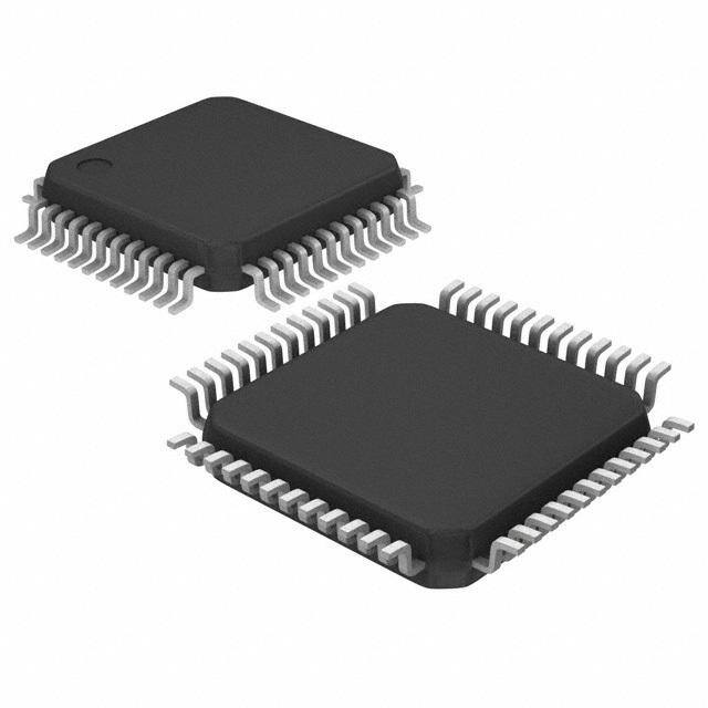
| 封装/外壳 | 48-LQFP |
| 工作温度 | -40°C ~ 85°C |
| 振荡器类型 | 内部 |
| 数据转换器 | A/D 8x12b |
| 标准包装 | 250 |
| 核心处理器 | ARM® Cortex™-M0 |
| 核心尺寸 | 32-位 |
| 电压-电源(Vcc/Vdd) | 2.5 V ~ 5.5 V |
| 程序存储器类型 | 闪存 |
| 程序存储容量 | 16KB(16K x 8) |
| 连接性 | EBI/EMI, I²C, IrDA, LIN, SPI, UART/USART |
| 速度 | 50MHz |


- 商务部:美国ITC正式对集成电路等产品启动337调查
- 曝三星4nm工艺存在良率问题 高通将骁龙8 Gen1或转产台积电
- 太阳诱电将投资9.5亿元在常州建新厂生产MLCC 预计2023年完工
- 英特尔发布欧洲新工厂建设计划 深化IDM 2.0 战略
- 台积电先进制程称霸业界 有大客户加持明年业绩稳了
- 达到5530亿美元!SIA预计今年全球半导体销售额将创下新高
- 英特尔拟将自动驾驶子公司Mobileye上市 估值或超500亿美元
- 三星加码芯片和SET,合并消费电子和移动部门,撤换高东真等 CEO
- 三星电子宣布重大人事变动 还合并消费电子和移动部门
- 海关总署:前11个月进口集成电路产品价值2.52万亿元 增长14.8%


PDF Datasheet 数据手册内容提取
™ NuMicro M052/M054BN Datasheet ™ ARM Cortex -M0 32-BIT MICROCONTROLLER ™ NuMicro Family M052/M054BN Datasheet Publication Release Date: Mar. 19, 2012 - 1 - Revision V1.01
™ NuMicro M052/M054BN Datasheet TABLE OF CONTENTS 1 GENERAL DESCRIPTION ··················································································································· 7 2 FEATURES ············································································································································ 8 3 BLOCK DIAGRAM ······························································································································ 13 4 SELECTION TABLE ··························································································································· 14 5 PIN CONFIGURATION ······················································································································· 15 5.1 QFN 33 pin ················································································································································ 15 5.2 LQFP 48 pin ·············································································································································· 16 5.3 Pin Description ·········································································································································· 17 6 FUNCTIONAL DESCRIPTION ··········································································································· 21 6.1 ARM® Cortex™-M0 Core ······················································································································· 21 6.2 System Manager ······································································································································ 23 6.2.1 Overview ······································································································································· 23 6.2.2 System Reset ······························································································································ 23 6.2.3 System Power Architecture ······································································································· 24 6.2.4 Whole System Memory Map ····································································································· 25 6.2.5 Whole System Memory Mapping Table ··················································································· 27 6.2.6 System Timer (SysTick) ············································································································· 27 6.2.7 Nested Vectored Interrupt Controller (NVIC) ·········································································· 29 6.3 Clock Controller ········································································································································ 30 6.3.1 Overview ······································································································································· 30 6.3.2 Clock Generator Block Diagram ······························································································· 30 6.3.3 System Clock & SysTick Clock ································································································· 32 6.3.4 AHB Clock Source Select ·········································································································· 33 6.3.5 Peripherals Clock Source Select ······························································································ 34 6.3.6 Power Down Mode (Deep Sleep Mode) Clock ······································································· 35 6.3.7 Frequency Divider Output ·········································································································· 35 6.4 General Purpose I/O ································································································································ 37 6.4.1 Overview ······································································································································· 37 6.5 I2C Serial Interface Controller (Master/Slave) ······················································································ 40 6.5.1 Overview ······································································································································· 40 6.5.2 Features········································································································································ 41 6.6 PWM Generator and Capture Timer ······································································································ 42 6.6.1 Overview ······································································································································· 42 6.6.2 Features········································································································································ 43 6.7 Serial Peripheral Interface (SPI) ············································································································ 44 6.7.1 Overview ······································································································································· 44 6.7.2 Features········································································································································ 44 Publication Release Date: Mar. 19, 2012 - 2 - Revision V1.01
™ NuMicro M052/M054BN Datasheet 6.8 Timer Controller ········································································································································ 45 6.8.1 Overview ······································································································································· 45 6.8.2 Features: ······································································································································ 45 6.9 Watchdog Timer (WDT) ··························································································································· 46 6.9.1 Overview ······································································································································· 46 6.9.2 Features········································································································································ 47 6.10 UART Interface Controller (UART) ······································································································ 48 6.10.1 Overview ······································································································································· 48 6.10.2 Features········································································································································ 50 6.11 Analog-to-Digital Converter (ADC) ······································································································ 51 6.11.1 Overview ······································································································································· 51 6.11.2 Features········································································································································ 51 6.12 External Bus Interface (EBI) ················································································································· 52 6.12.1 Overview ······································································································································· 52 6.12.2 Features········································································································································ 52 6.13 Flash Memory Controller (FMC) ·········································································································· 53 6.13.1 Overview ······································································································································· 53 6.13.2 Features········································································································································ 53 7 TYPICAL APPLICATION CIRCUIT ··································································································· 54 8 ELECTRICAL CHARACTERISTICS ·································································································· 55 8.1 Absolute Maximum Ratings ···················································································································· 55 8.2 DC Electrical Characteristics ·················································································································· 56 8.3 AC Electrical Characteristics ·················································································································· 60 8.3.1 External Crystal ··························································································································· 60 8.3.2 External Oscillator ······················································································································· 60 8.3.3 Typical Crystal Application Circuits ·························································································· 61 8.3.4 Internal 22.1184 MHz RC Oscillator ························································································· 62 8.3.5 Internal 10kHz RC Oscillator ····································································································· 62 8.4 Analog Characteristics ····························································································································· 63 8.4.1 Specification of 12-bit SARADC ································································································ 63 8.4.2 Specification of LDO & Power management ··········································································· 64 8.4.3 Specification of Low Voltage Reset ·························································································· 65 8.4.4 Specification of Brown-Out Detector ························································································ 65 8.4.5 Specification of Power-On Reset (5V) ····················································································· 65 8.4.6 Specification of Temperature Sensor ······················································································· 66 8.4.7 Specification of Comparator ······································································································ 66 8.5 Flash DC Electrical Characteristics ······································································································· 67 9 PACKAGE DIMENSIONS ··················································································································· 68 9.1 LQFP-48 (7x7x1.4mm2 Footprint 2.0mm) ····························································································· 68 Publication Release Date: Mar. 19, 2012 - 3 - Revision V1.01
™ NuMicro M052/M054BN Datasheet 9.2 QFN-33 (5X5 mm2, Thickness 0.8mm, Pitch 0.5 mm) ········································································ 69 10 REVISION HISTORY ··························································································································· 70 Publication Release Date: Mar. 19, 2012 - 4 - Revision V1.01
™ NuMicro M052/M054BN Datasheet LIST OF FIGURES Figure 3-1 NuMicro M051 Series Block Diagram ........................................................................ 13 Figure 4-1 NuMicro Naming Rule ................................................................................................ 14 Figure 5-1 NuMicro M051 Series QFN33 Pin Diagram ............................................................... 15 Figure 5-2 NuMicro M051 Series LQFP-48 Pin Diagram ........................................................... 16 Figure 6-1 Functional Block Diagram ............................................................................................. 21 Figure 6-2 NuMicro M051™ Series Power Architecture Diagram .................................................. 24 Figure 6-3 Clock generator block diagram ..................................................................................... 31 Figure 6-4 System Clock Block Diagram ....................................................................................... 32 Figure 6-5 SysTick clock Control Block Diagram ........................................................................... 32 Figure 6-6 AHB Clock Source for HCLK ........................................................................................ 33 Figure 6-7 Peripherals Clock Source Select for PCLK .................................................................. 34 Figure 6-8 Clock Source of Frequency Divider .............................................................................. 35 Figure 6-9 Block Diagram of Frequency Divider ............................................................................ 36 Figure 6-10 Push-Pull Output......................................................................................................... 37 Figure 6-11 Open-Drain Output ..................................................................................................... 38 Figure 6-12 Quasi-bidirectional I/O Mode ...................................................................................... 39 Figure 6-13 I2C Bus Timing ............................................................................................................ 40 Figure 6-14 Timing of Interrupt and Reset Signal .......................................................................... 47 Figure 8-1 Typical Crystal Application Circuit ................................................................................ 61 Publication Release Date: Mar. 19, 2012 - 5 - Revision V1.01
™ NuMicro M052/M054BN Datasheet LIST OF TABLES Table 4-1 NuMicro M051 Series Product Selection Guide ......................................................... 14 Table 5-1 NuMicro M051 Series Pin Description ........................................................................ 20 Table 6-1 Address Space Assignments for On-Chip Modules ...................................................... 26 Table 6-2 Watchdog Timeout Interval Selection ............................................................................ 47 Table 6-3 UART Baud Rate Equation ............................................................................................ 48 Table 6-4 UART Baud Rate Setting Table ..................................................................................... 49 Publication Release Date: Mar. 19, 2012 - 6 - Revision V1.01
™ NuMicro M052/M054BN Datasheet 1 GENERAL DESCRIPTION The NuMicro M051™ series is a 32-bit microcontroller with embedded ARM® Cortex™-M0 core for industrial control and applications which need rich communication interfaces. The Cortex™-M0 is the newest ARM embedded processor with 32-bit performance and at a cost equivalent to traditional 8-bit microcontroller. The NuMicro M051™ series includes M052, M054, M058 and M0516 families. The M052/M054 can run up to 50 MHz. Thus it can afford to support a variety of industrial control and applications which need high CPU performance. The M052/M054 has 8K/16K-byte embedded flash, 4K-byte data flash, 4K-byte flash for the ISP, and 4K-byte embedded SRAM. Many system level peripheral functions, such as I/O Port, EBI (External Bus Interface), Timer, UART, SPI, I2C, PWM, ADC, Watchdog Timer and Brownout Detector, have been incorporated into the M052/M054 in order to reduce component count, board space and system cost. These useful functions make the M052/M054 powerful for a wide range of applications. Additionally, the M052/M054 is equipped with ISP (In-System Programming) and ICP (In-Circuit Programming) functions, which allow the user to update the program memory without removing the chip from the actual end product. Publication Release Date: Mar. 19, 2012 - 7 - Revision V1.01
™ NuMicro M052/M054BN Datasheet 2 FEATURES Core ARM® Cortex™-M0 core runs up to 50 MHz. One 24-bit system timer. Supports low power sleep-mode. A single-cycle 32-bit hardware multiplier. NVIC for the 32 interrupt inputs, each with 4-levels of priority. Supports Serial Wire Debug (SWD) interface and 2 watchpoints/4 breakpoints. Built-in LDO for Wide Operating Voltage Range: 2.5V to 5.5V Memory 8KB/16KB Flash memory for program memory (APROM) 4KB Flash memory for data memory (DataFlash) 4KB Flash memory for loader (LDROM) 4KB SRAM for internal scratch-pad RAM (SRAM) Clock Control Programmable system clock source 4~24 MHz external crystal input 22.1184 MHz internal oscillator (trimmed to 3% accuracy) 10 kHz low-power oscillator for Watchdog Timer and wake-up in sleep mode PLL allows CPU operation up to the maximum 50MHz I/O Port Up to 40 general-purpose I/O (GPIO) pins for LQFP-48 package Four I/O modes: Quasi bi-direction Push-Pull output Publication Release Date: Mar. 19, 2012 - 8 - Revision V1.01
™ NuMicro M052/M054BN Datasheet Open-Drain output Input only with high impendence TTL/Schmitt trigger input selectable I/O pin can be configured as interrupt source with edge/level setting Supports high driver and high sink IO mode Timer Provides four channel 32-bit timers, one 8-bit pre-scale counter with 24-bit up-timer for each timer. Independent clock source for each timer. 24-bit timer value is readable through TDR (Timer Data Register) Provides one-shot, periodic and toggle operation modes. Provide event counter function. Provide external capture/reset counter function equivalent to 8051 Timer2. Watchdog Timer Multiple clock sources Supports wake up from power down or sleep mode Interrupt or reset selectable on watchdog time-out PWM Built-in up to four 16-bit PWM generators; providing eight PWM outputs or four complementary paired PWM outputs Individual clock source, clock divider, 8-bit pre-scalar and dead-zone generator for each PWM generator PWM interrupt synchronized to PWM period 16-bit digital Capture timers (shared with PWM timers) with rising/falling capture inputs Supports capture interrupt UART Publication Release Date: Mar. 19, 2012 - 9 - Revision V1.01
™ NuMicro M052/M054BN Datasheet Up to two sets of UART device Programmable baud-rate generator Buffered receiver and transmitter, each with 15 bytes FIFO Optional flow control function (CTS and RTS) Supports IrDA(SIR) function Supports RS485 function Supports LIN function SPI Up to two sets of SPI device. Supports master/slave mode Full duplex synchronous serial data transfer Provide 3 wire function Variable length of transfer data from 1 to 32 bits MSB or LSB first data transfer Rx latching data can be either at rising edge or at falling edge of serial clock Tx sending data can be either at rising edge or at falling edge of serial clock Supports Byte suspend mode in 32-bit transmission I2C Supports master/slave mode Bidirectional data transfer between masters and slaves Multi-master bus (no central master). Arbitration between simultaneously transmitting masters without corruption of serial data on the bus Serial clock synchronization allows devices with different bit rates to communicate via one serial bus. Publication Release Date: Mar. 19, 2012 - 10 - Revision V1.01
™ NuMicro M052/M054BN Datasheet Serial clock synchronization can be used as a handshake mechanism to suspend and resume serial transfer. Programmable clocks allow versatile rate control. Supports multiple address recognition (four slave address with mask option) ADC 12-bit SAR ADC with 760k SPS Up to 8-ch single-ended input or 4-ch differential input Supports single mode/burst mode/single-cycle scan mode/continuous scan mode Supports 2’ complement/un-signed format in differential mode conversion result Each channel with an individual result register Supports conversion value monitoring (or comparison) for threshold voltage detection Conversion can be started either by software trigger or external pin trigger Analog Comparator Up to 2 comparator analog modules External input or internal band gap voltage selectable at negative node Interrupt when compare result change Power down wake up EBI (External Bus Interface) for external memory-mapped device access Accessible space: 64KB in 8-bit mode or 128KB in 16-bit mode Supports 8-bit/16-bit data width Supports byte-write in 16-bit data width In-System Programming (ISP) and In-Circuit Programming (ICP) One built-in temperature sensor with 1℃ resolution Brown-Out Detector With 4 levels: 4.3V/3.7V/2.7V/2.2V Publication Release Date: Mar. 19, 2012 - 11 - Revision V1.01
™ NuMicro M052/M054BN Datasheet Supports Brown-Out interrupt and reset option 96-bit unique ID LVR (Low Voltage Reset) Threshold voltage levels: 2.0V Operating Temperature: -40℃~85℃ Packages: Green package (RoHS) 48-pin LQFP, 33-pin QFN Publication Release Date: Mar. 19, 2012 - 12 - Revision V1.01
™ NuMicro M052/M054BN Datasheet 3 BLOCK DIAGRAM CONFIG 10K OSC Cortex-M0 CLK_CTL DATAFLASH 4KB 50 MHz P 22M OSC LDROM ISP 4KB L EXT. 4~24M L XTAL LDO 2.5 ~ 5.5V APROM SRAM GPIO 4KB P0~P4 16KB(M054) 8KB(M052) ADC 8ch/12bit Watch Dog Timer ADC SARADC 760K SPS AD[15:0] SPI 0/1 Timer 0/1 nCS UART 0/1 PAD Control nRD nWR EBI Timer 2/3 PWM 0~7 POR mclk I2C BOD ALE nWRL LVR nWRH Analog Comparator Figure 3-1 NuMicro M051 Series Block Diagram Publication Release Date: Mar. 19, 2012 - 13 - Revision V1.01
™ NuMicro M052/M054BN Datasheet 4 SELECTION TABLE NuMicro M051™ Series Selection Guide Data Connectivity ISP Part number APROM RAM LDROM I/O Timer COMP PWM ADC EBI Package Flash ICP UART SPI I2C M052LBN 8KB 4KB 4KB 4KB 40 4x32-bit 2 2 1 2 8 8X12-bit v v LQFP48 M052ZBN 8KB 4KB 4KB 4KB 24 4x32-bit 2 1 1 2 5 8X12-bit v QFN33 M054LBN 16KB 4KB 4KB 4KB 40 4x32-bit 2 2 1 2 8 8X12-bit v v LQFP48 M054ZBN 16KB 4KB 4KB 4KB 24 4x32-bit 2 1 1 2 5 8X12-bit v QFN33 Table 4-1 NuMicro M051 Series Product Selection Guide MM005X -- XX XX XX CPU core ARM Cortex M0 Part Number Temperature NN :: -- 4400℃℃ ~~ ++8855℃℃ 5522 :: 88KK FFllaasshh RROOMM EE :: -- 4400℃℃ ~~++110055℃℃ 5544 :: 1166KK FFllaasshh RROOMM CC :: -- 4400℃℃ ~~++112255℃℃ Package Reserved L : LQFP 48 Z : QFN 33 Figure 4-1 NuMicro Naming Rule Publication Release Date: Mar. 19, 2012 - 14 - Revision V1.01
™ NuMicro M052/M054BN Datasheet 5 PIN CONFIGURATION 5.1 QFN 33 pin CPN0, A TXD1, A RXD1, A AIN0 TXD1, C RXD1, R IN IN IN , T TS TS 4 3 2 2 1 1 , P , P , P , P A , P , P 1 1 1 1 V V 0 0 .4 .3 .2 .0 DD DD .0 .1 32 31 30 29 28 27 26 25 CPP0, AIN5, P1.5 1 24 P0.4, SPISS1 RST 2 23 P0.5, MOSI_1 CPN1, RXD, P3.0 3 22 P0.6, MISO_1 AV 4 21 P0.7, SCLK1 SS QFN 33-Pin CPP1, TXD, P3.1 5 20 P4.7, ICE_DAT T0EX, STADC, INT0, P3.2 6 19 P4.6, ICE_CLK SDA, T0, P3.4 7 18 P2.6, PWM6, CPO1 33 VSS SCL, T1, P3.5 8 17 P2.5, PWM5 9 10 11 12 13 14 15 16 P X X V L P P P 3 T T S D 2 2 2 .6 A A S O .2 .3 .4 , C L2 L1 _C , P , P , P K A W W W O P M M M , C 2 3 4 P O 0Top transparent view Figure 5-1 NuMicro M051 Series QFN33 Pin Diagram Publication Release Date: Mar. 19, 2012 - 15 - Revision V1.01
™ NuMicro M052/M054BN Datasheet 5.2 LQFP 48 pin C PWM2, P4.2 PN0, SPISS0,AIN4,P1.4 TXD1,AIN3,P1.3 RXD1,AIN2, P1.2 nWRH, T3,AIN1,P1.1 nWRL, T2,AIN0,P1.0 DDAV DDV TXD1, CTS1, AD0, P0.0 RXD1, RTS1, AD1, P0.1 TXD, CTS0, AD2, P0.2 RXD, RTS0, AD3, P0.3 4 4 4 4 4 4 4 4 4 3 3 3 8 7 6 5 4 3 2 1 0 9 8 7 CPP0, MOSI_0, AIN5, P1.5 1 36 P4.1, PWM1, T3EX MISO_0, AIN6, P1.6 2 35 P0.4, AD4, SPISS1 SPICLK0, AIN7, P1.7 3 34 P0.5, AD5, MOSI_1 RST 4 33 P0.6, AD6, MISO_1 CPN1, RXD, P3.0 5 32 P0.7, AD7, SPICLK1 AVSS 6 48-pin LQFP 31 P4.7, ICE_DAT CPP1, TXD, P3.1 7 30 P4.6, ICE_CLK T0EX, STADC, INT0, P3.2 8 29 P4.5, ALE T1EX, MCLK, INT1, P3.3 9 28 P4.4, /CS SDA, T0, P3.4 10 27 P2.7, AD15, PWM7 SCL, T1, P3.5 11 26 P2.6, AD14, PWM6, CPO1 PWM3, P4.3 12 25 P2.5, AD13, PWM5 1 1 1 1 1 1 1 2 2 2 2 2 3 4 5 6 7 8 9 0 1 2 3 4 P P X X V L P P P P P P 3.6 3.7 TA TA SS DO 2.0 2.1 2.2 2.3 2.4 4.0 , W , R L2 L1 _C , A , A , A , A , A , P R, CKO, CP D AP D8, PWM0 D9, PWM1 D10, PWM2 D11, PWM3 D12, PWM4 WM0, T2EX O 0 Figure 5-2 NuMicro M051 Series LQFP-48 Pin Diagram Publication Release Date: Mar. 19, 2012 - 16 - Revision V1.01
™ NuMicro M052/M054BN Datasheet 5.3 Pin Description Pin number Alternate Function Symbol Type[1] Description QFN33 LQFP48 1 2 3 CRYSTAL1: This is the input pin to the internal I inverting amplifier. The system clock is from 11 16 XTAL1 external crystal or resonator when FOSC[1:0] (ST) (CONFIG3[1:0]) are both logic 1 by default. CRYSTAL2: This is the output pin from the 10 15 XTAL2 O internal inverting amplifier. It emits the inverted signal of XTAL1. POWER SUPPLY: Power supply to I/O ports 27 41 VDD P and LDO source for internal PLL and digital circuit. 12 GROUND: Digital Ground potential. 17 VSS P 33 POWER SUPPLY: Power supply to internal 28 42 AVDD P analog circuit. 4 6 AVSS P GROUND: Analog Ground potential. LDO: LDO output pin 13 18 LDO_CAP P Note: It needs to be connected with a 1uF capacitor. RESET: /RST pin is a Schmitt trigger input pin for hardware device reset. A “Low” on this pin for 768 clock counter of Internal RC 22M while I 2 4 RST the system clock is running will reset the (ST) device. /RST pin has an internal pull-up resistor allowing power-on reset by simply connecting an external capacitor to GND. 26 40 P0.0 CTS1 AD0 TXD1[2] D, PORT0: Port 0 is an 8-bit four mode output pin I/O and two mode input. Its multifunction pins are for CTS1, RTS1, CTS0, RTS0, SPISS1, MOSI_1, MISO_1, and SPICLK1. 25 39 P0.1 RTS1 AD1 RXD1[2] D, I/O P0 has an alternative function as AD[7:0] while external memory accessing. During the external memory access, P0 will output high NC 38 P0.2 CTS0 AD2 TXD[2] D, will be internal strong pulled-up rather than I/O weak pull-up in order to drive out high byte Publication Release Date: Mar. 19, 2012 - 17 - Revision V1.01
™ NuMicro M052/M054BN Datasheet Pin number Alternate Function Symbol Type[1] Description QFN33 LQFP48 1 2 3 NC 37 P0 .3 RT S0 AD 3 RXD [2] D , address for external devices. I/O These pins which are SPISS1, MOSI_1, MISO_1, and SPICLK1 for the SPI function D, used. 24 35 P0.4 SPISS1 AD4 I/O CTS0/1: Clear to Send input pin for UART0/1 RTS0/1: Request to Send output pin for D, 23 34 P0.5 MOSI_1 AD5 UART0/1 I/O The RXD/TXD pins are for UART0 function used. D, 22 33 P0.6 MISO_1 AD6 I/O The RXD1/TXD1 pins are for UART1 function used. D, 21 32 P0.7 SPICLK1 AD7 I/O 29 43 P1.0 T2 AIN0 WRL I/O PORT1: Port 1 is an 8-bit four mode output pin and two mode input. Its multifunction pins are for T2, T3, RXD1, TXD1, SPISS0, MOSI_0, MISO_0, and SPICLK0. NC 44 P1.1 T3 AIN1 I/O WRH These pins which are SPISS0, MOSI_0, MISO_0, and SCLK0 for the SPI function used. 30 45 P1.2 RXD1[3] AIN2 I/O These pins which are AIN0~AIN7for the 12 bits ADC function used. 31 46 P1.3 TXD1[3] AIN3 I/O The RXD1/TXD1 pins are for UART1 function used. 32 47 P1.4 SPISS0 AIN4 CPN0 I/O TheWRL /WRH pins are for low/high byte write enable output in 16-bit data width of EBI. 1 1 P1.5 MOSI_0 AIN5 CPP0 I/O The CPN0/CPP0 pins are for Comparator0 negative/positive inputs. NC 2 P1.6 MISO_0 AIN6 I/O The T2/T3 pins are for Timer2/3 external even counter input. NC 3 P1.7 SPICLK0 AIN7 I/O NC 19 P2.0 PWM0[2] AD8 D, PORT2: Port 2 is an 8-bit four mode output pin I/O and two mode input. It has an alternative function NC 20 P2.1 PWM1[2] AD9 D, P2 has an alternative function as AD[15:8] I/O while external memory accessing. During the external memory access, P2 will output high will be internal strong pulled-up rather than 14 21 P2.2 PWM2[2] AD10 D, weak pull-up in order to drive out high byte I/O address for external devices. These pins which are PWM0~PWM7 for the 15 22 P2.3 PWM3[2] AD11 D, PWM function used in the LQFP48 package. I/O Publication Release Date: Mar. 19, 2012 - 18 - Revision V1.01
™ NuMicro M052/M054BN Datasheet Pin number Alternate Function Symbol Type[1] Description QFN33 LQFP48 1 2 3 16 2 3 P2 .4 PWM 4[2] AD 12 D , The CPO1 pin is the output of Comparator1. I/O 17 25 P2.5 PWM5[2] AD13 D, I/O 18 26 P2.6 PWM6[2] AD14 CPO1 D, I/O NC 27 P2.7 PWM7[2] AD15 D, I/O 3 5 P3.0 RXD[2] CPN1 I/O PORT3: Port 3 is an 8-bit four mode output pin and two mode input. Its multifunction pins are 5 7 P3.1 TXD[2] CPP1 I/O INT0 INT1 for RXD, TXD, , , T0, T1, WR , RD 6 8 P3.2 INT0 STADC T0EX I/O and . The RXD/TXD pins are for UART0 function used. NC 9 P3.3 INT1 MCLK T1EX I/O The SDA/SCK pins are for I2C function used. MCLK: EBI clock output pin. 7 10 P3.4 T0 SDA I/O CKO: HCLK clock output The STADC pin is for ADC external trigger 8 11 P3.5 T1 SCL I/O input. The CPN1/CPP1 pins are for Comparator1 negative/positive inputs. 9 13 P3.6 WR CKO CPO0 I/O The CPO0 pin is the output of Comparator0. The T0/T1 pins are for Timer0/1 external even counter input. NC 14 P3.7 RD I/O The T0EX/T1EX pins are for external capture/reset trigger input of Timer0/1. NC 24 P4.0 PWM0[2] T2EX I/O PORT4: Port 4 is an 8-bit four mode output pin and two mode input. Its multifunction pins are for /CS, ALE, ICE_CLK and ICE_DAT. NC 36 P4.1 PWM1[2] T3EX I/O CS for EBI (External Bus Interface) used. NC 48 P4.2 PWM2[2] I/O ALE (Address Latch Enable) is used to enable the address latch that separates the address NC 12 P4.3 PWM3[2] I/O from the data on Port 0 and Port 2. Publication Release Date: Mar. 19, 2012 - 19 - Revision V1.01
™ NuMicro M052/M054BN Datasheet Pin number Alternate Function Symbol Type[1] Description QFN33 LQFP48 1 2 3 The ICE_CLK/ICE_DAT pins are for JTAG-ICE NC 28 P4.4 CS I/O function used. PWM0-3 can be used from P4.0-P4.3 when NC 29 P4.5 ALE I/O EBI is active. The T2EX/T3EX pins are for external 19 30 P4.6 ICE_CLK I/O capture/reset trigger input of Timer2/3. 20 31 P4.7 ICE_DAT I/O Table 5-1 NuMicro M051 Series Pin Description [1] I/O type description. I: input, O: output, I/O: quasi bi-direction, D: open-drain, P: power pins, ST: Schmitt trigger. [2] The pins features which are set by S/W. Only one-set pin can be used while S/W to set it. Publication Release Date: Mar. 19, 2012 - 20 - Revision V1.01
™ NuMicro M052/M054BN Datasheet 6 FUNCTIONAL DESCRIPTION 6.1 ARM® Cortex™-M0 Core The Cortex™-M0 processor is a configurable, multistage, 32-bit RISC processor. It has an AMBA AHB- Lite interface and includes an NVIC component. It also has optional hardware debug functionality. The processor can execute Thumb code and is compatible with other Cortex-M profile processor. The profile supports two modes -Thread and Handler modes. Handler mode is entered as a result of an exception. An exception return can only be issued in Handler mode. Thread mode is entered on Reset, and can be entered as a result of an exception return. Figure 6-1 shows the functional controller of processor. Cortex-M0 components Cortex-M0 processor Debug Interrupts Nested Vectored Cortex-M0 Breakpoint and Interrupt Processor Watchpoint Controller Core Unit (NVIC) Wakeup Interrupt Debug Controller Bus matrix Debugger Access Port (WIC) interface (DAP) AHB-Lite interface Serial Wire or JTAG debug port Figure 6-1 Functional Block Diagram The implemented device provides: A low gate count processor the features: The ARMv6-M Thumb® instruction set. Thumb-2 technology. ARMv6-M compliant 24-bit SysTick timer. A 32-bit hardware multiplier. The system interface supports little-endian data accesses. The ability to have deterministic, fixed-latency, interrupt handling. Publication Release Date: Mar. 19, 2012 - 21 - Revision V1.01
™ NuMicro M052/M054BN Datasheet Load/store-multiples and multicycle-multiplies that can be abandoned and restarted to facilitate rapid interrupt handling. C Application Binary Interface compliant exception model. This is the ARMv6-M, C Application Binary Interface(C-ABI) compliant exception model that enables the use of pure C functions as interrupt handlers. Low power sleep-mode entry using Wait For Interrupt (WFI), Wait For Event(WFE) instructions, or the return from interrupt sleep-on-exit feature. NVIC features: 32 external interrupt inputs, each with four levels of priority. Dedicated non-Maskable Interrupt (NMI) input. Support for both level-sensitive and pulse-sensitive interrupt lines Wake-up Interrupt Controller (WIC), supports ultra-low power sleep mode. Debug support: Four hardware breakpoints. Two watchpoints. Program Counter Sampling Register (PCSR) for non-intrusive code profiling. Single step and vector catch capabilities. Bus interfaces: Single 32-bit AMBA-3 AHB-Lite system interface that provides simple integration to all system peripherals and memory. Single 32-bit slave port that supports the DAP (Debug Access Port). Publication Release Date: Mar. 19, 2012 - 22 - Revision V1.01
™ NuMicro M052/M054BN Datasheet 6.2 System Manager 6.2.1 Overview The following functions are included in system manager section System Resets System Memory Map System management registers for Part Number ID, chip reset and on-chip module reset , multi-functional pin control System Timer (SysTick) Nested Vectored Interrupt Controller (NVIC) System Control registers 6.2.2 System Reset The system reset includes one of the list below event occurs. For these reset event flags can be read by RSTSRC register. The Power-On Reset (POR) The low level on the /RESET pin Watchdog Time Out Reset (WDT) Low Voltage Reset (LVR) Brown-Out Detected Reset (BOD) CPU Reset Software one shot Reset Publication Release Date: Mar. 19, 2012 - 23 - Revision V1.01
™ NuMicro M052/M054BN Datasheet 6.2.3 System Power Architecture In this device, the power architecture is divided into three segments. Analog power from AV and AV provides the power for analog module operation. DD SS Digital power from V and V supplies the power to the internal regulator which DD SS provides a fixed 1.8V power for digital operation and I/O pins. The outputs of internal voltage regulator, which is LDO, require an external capacitor which should be located close to the corresponding pin. The Figure 6-2 shows the power architecture of this device. M051 Series Power Analog Comparator Distribution 12-bit AVDD SAR-ADC Low Brown AVSS Voltage Out Reset Detector Internal Temperature FLASH Digital Logic 22.1184 MHz & 10 kHz Seneor Oscillator LDO 1.8V 1uF POR18 5V to 1.8V PLL IO cell P0 - P4 LDO POR50 S D S S D S V V V P Figure 6-2 NuMicro M051™ Series Power Architecture Diagram Publication Release Date: Mar. 19, 2012 - 24 - Revision V1.01
™ NuMicro M052/M054BN Datasheet 6.2.4 Whole System Memory Map NuMicro M051™ series provides a 4G-byte address space. The memory locations assigned to each on-chip modules are shown in Table 6-1. The detailed register memory addressing and programming will be described in the following sections for1 individual on-chip peripherals. NuMicro M051™ series only supports little-endian data format. Address Space Token Modules Flash & SRAM Memory Space 0x0000_0000 – 0x0000_FFFF FLASH_BA FLASH Memory Space (64KB) 0x2000_0000 – 0x2000_0FFF SRAM_BA SRAM Memory Space (4KB) EBI Space (0x6000_0000 ~ 0x6001_FFFF) 0x6000_0000 – 0x6001_FFFF EBI_BA External Memory Space (128KB) AHB Modules Space (0x5000_0000 – 0x501F_FFFF) 0x5000_0000 – 0x5000_01FF GCR_BA System Global Control Registers 0x5000_0200 – 0x5000_02FF CLK_BA Clock Control Registers 0x5000_0300 – 0x5000_03FF INT_BA Interrupt Multiplexer Control Registers 0x5000_4000 – 0x5000_7FFF GPIO_BA GPIO (P0~P4) Control Registers 0x5000_C000 – 0x5000_FFFF FMC_BA Flash Memory Control Registers 0x5001_0000 – 0x5001_03FF EBI_CTL_BA EBI Control Registers (128KB) APB Modules Space (0x4000_0000 ~ 0x400F_FFFF) 0x4000_4000 – 0x4000_7FFF WDT_BA Watch-Dog Timer Control Registers 0x4001_0000 – 0x4001_3FFF TMR01_BA Timer0/Timer1 Control Registers 0x4002_0000 – 0x4002_3FFF I2C_BA I2C Interface Control Registers 0x4003_0000 – 0x4003_3FFF SPI0_BA SPI0 with master/slave function Control Registers 0x4003_4000 – 0x4003_7FFF SPI1_BA SPI1 with master/slave function Control Registers 0x4004_0000 – 0x4004_3FFF PWMA_BA PWM0/1/2/3 Control Registers Publication Release Date: Mar. 19, 2012 - 25 - Revision V1.01
™ NuMicro M052/M054BN Datasheet 0x4005_0000 – 0x4005_3FFF UART0_BA UART0 Control Registers 0x400D_0000 – 0x400D_3FFF ACMP_BA Analog Comparator Control Registers 0x400E_0000 – 0x400E_FFFF ADC_BA Analog-Digital-Converter (ADC) Control Registers 0x4011_0000 – 0x4011_3FFF TMR23_BA Timer2/Timer3 Control Registers 0x4014_0000 – 0x4014_3FFF PWMB_BA PWM4/5/6/7 Control Registers 0x4015_0000 – 0x4015_3FFF UART1_BA UART1 Control Registers System Control Space (0xE000_E000 ~ 0xE000_EFFF) 0xE000_E010 – 0xE000_E0FF SCS_BA System Timer Control Registers 0xE000_E100 – 0xE000_ECFF SCS_BA External Interrupt Controller Control Registers 0xE000_ED00 – 0xE000_ED8F SCS_BA System Control Registers Table 6-1 Address Space Assignments for On-Chip Modules Publication Release Date: Mar. 19, 2012 - 26 - Revision V1.01
™ NuMicro M052/M054BN Datasheet 6.2.5 Whole System Memory Mapping Table M052/54/58/516 4 GB 0xFFFF_FFFF Reserved | System Control 0xE000_F000 System Timer Control 0xE000_E000 SCS_BA 0xE000_EFFF System Control 0xE000_E000 0xE000_E00F Reserved | 0x6002_0000 0x6001_FFFF EBI 0x6000_0000 0x5FFF_FFFF Reserved | 0x5020_0000 AHB peripherals 0x501F_FFFF EBI Control 0x5001_0000 EBI_CTL_BA AHB 0x5000_0000 FMC 0x5000_C000 FLASH_BA 0x4FFF_FFFF GPIO Control 0x5000_4000 GPIO_BA Interrupt Multiplexer Control 0x5000_0300 INT_BA Reserved | Clock Control 0x5000_0200 CLK_BA 0x4020_0000 System Global Control 0x5000_0000 GCR_BA 0x401F_FFFF APB | 1 GB 0x4000_0000 0x3FFF_FFFF APB peripherals Reserved | UART1 Control 0x4015_0000 UART1_BA 0x2000_1000 PWM4/5/6/7 Control 0x4014_0000 PWMB_BA 0x2000_0FFF Timer2/Timer3 Control 0x4011_0000 TMR23_BA ADC Control 0x400E_0000 ADC_BA 4 KB SRAM | COMP control 0x400D_0000 ACMP_BA (M052/M054/M058/M0516) UART0 Control 0x4005_0000 UART0_BA 0.5 GB 0x2000_0000 PWM0/1/2/3 Control 0x4004_0000 PWMA_BA 0x1FFF_FFFF SPI1 Control 0x4003_4000 SPI1_BA SPI0 Control 0x4003_0000 SPI0_BA Reserved | I2C Control 0x4002_0000 I2C_BA 0x0001_0000 Timer0/Timer1 Control 0x4001_0000 TMR01_BA 64 KB on-chip Flash (M0516) 0x0000_FFFF WDT Control 0x4000_4000 WDT_BA 32 KB on-chip Flash (M058) 0x0000_7FFF 16 KB on-chip Flash (M054) 0x0000_3FFF 0x0000_1FFF 8 KB on-chip Flash (M052) 0 GB 0x0000_0000 6.2.6 System Timer (SysTick) The Cortex-M0 includes an integrated system timer, SysTick. SysTick provides a simple, 24-bit Publication Release Date: Mar. 19, 2012 - 27 - Revision V1.01
™ NuMicro M052/M054BN Datasheet clear-on-write, decrementing, wrap-on-zero counter with a flexible control mechanism. The counter can be used as a Real Time Operating System (RTOS) tick timer or as a simple counter. When system timer is enabled, it will count down from the value in the SysTick Current Value Register (SYST_CVR) to zero, and reload (wrap) to the value in the SysTick Reload Value Register (SYST_RVR) on the next clock edge, then decrement on subsequent clocks. When the counter transitions to zero, the COUNTFLAG status bit is set. The COUNTFLAG bit clears on reads. The SYST_CVR value is UNKNOWN on reset. Software should write to the register to clear it to zero before enabling the feature. This ensures the timer will count from the SYST_RVR value rather than an arbitrary value when it is enabled. If the SYST_RVR is zero, the timer will be maintained with a current value of zero after it is reloaded with this value. This mechanism can be used to disable the feature independently from the timer enable bit. For more detailed information, please refer to the documents “ARM® Cortex™-M0 Technical Reference Manual” and “ARM® v6-M Architecture Reference Manual”. Publication Release Date: Mar. 19, 2012 - 28 - Revision V1.01
™ NuMicro M052/M054BN Datasheet 6.2.7 Nested Vectored Interrupt Controller (NVIC) Cortex-M0 provides an interrupt controller as an integral part of the exception mode, named as “Nested Vectored Interrupt Controller (NVIC)”. It is closely coupled to the processor kernel and provides following features: Nested and Vectored interrupt support Automatic processor state saving and restoration Dynamic priority changing Reduced and deterministic interrupt latency The NVIC prioritizes and handles all supported exceptions. All exceptions are handled in “Handler Mode”. This NVIC architecture supports 32 (IRQ[31:0]) discrete interrupts with 4 levels of priority. All of the interrupts and most of the system exceptions can be configured to different priority levels. When an interrupt occurs, the NVIC will compare the priority of the new interrupt to the current running one’s priority. If the priority of the new interrupt is higher than the current one, the new interrupt handler will override the current handler. When any interrupts is accepted, the starting address of the interrupt service routine (ISR) is fetched from a vector table in memory. There is no need to determine which interrupt is accepted and branch to the starting address of the correlated ISR by software. While the starting address is fetched, NVIC will also automatically save processor state including the registers “PC, PSR, LR, R0~R3, R12” to the stack. At the end of the ISR, the NVIC will restore the mentioned registers from stack and resume the normal execution. Thus it will take less and deterministic time to process the interrupt request. The NVIC supports “Tail Chaining” which handles back-to-back interrupts efficiently without the overhead of states saving and restoration and therefore reduces delay time in switching to pending ISR at the end of current ISR. The NVIC also supports “Late Arrival” which improves the efficiency of concurrent ISRs. When a higher priority interrupt request occurs before the current ISR starts to execute (at the stage of state saving and starting address fetching), the NVIC will give priority to the higher one without delay penalty. Thus it advances the real-time capability. For more detailed information, please refer to the documents “ARM® Cortex™-M0 Technical Reference Manual” and “ARM® v6-M Architecture Reference Manual”. Publication Release Date: Mar. 19, 2012 - 29 - Revision V1.01
™ NuMicro M052/M054BN Datasheet 6.3 Clock Controller 6.3.1 Overview The clock controller generates the clocks for the whole chip, including system clocks and all peripheral clocks. The clock controller also implements the power control function with the individually clock ON/OFF control, clock source selection and clock divider. The chip will not enter power-down mode until CPU sets the power down enable bit (PWR_DOWN_EN) and Cortex-M0 core executes the WFI instruction. After that, chip enter power-down mode and wait for wake-up interrupt source triggered to leave power-down mode. In the power down mode, the clock controller turns off the external crystal and internal 22.1184 MHz oscillator to reduce the overall system power consumption. 6.3.2 Clock Generator Block Diagram The clock generator consists of 4 sources which list below: One external 4~24 MHz crystal One internal 22.1184 MHz RC oscillator One programmable PLL FOUT(PLL source consists of external 4~24 MHz crystal and internal 22.1184M) One internal 10 kHz oscillator Publication Release Date: Mar. 19, 2012 - 30 - Revision V1.01
™ NuMicro M052/M054BN Datasheet 22.1184 22.1184 MHz MHz 111 CPUCLK CPU 10 kHz 4~12 011 MHz PLLFOUT 010 1/(HCLK_N+1) HCLK EBI Reserved 10 kHz 001 ACMP 4~24 MHz PCLK I2C 000 SPI 0-1 CLKSEL0[2:0] 22.1184 MHz 111 HCLK TMR 0 010 TMR 1 22.1184 MHz 1 Reserved 001 TMR 2 4~24 MHz 0 PLLFOUT 4~24 MHz 000 TMR 3 PLLCON[19] CLKSEL1[22:20] 22.1184 MHz FMC CLKSEL1[18:16] 22.1184 MHz 1/2 111 CLKSEL1[14:12] CLKSEL1[10:8] HCLK CPUCLK 1/2 011 1 4~24 MHz SysTick 1/2 010 0 Reserved 001 SYST_CSR[2] 4~24 MHz 000 22.1184 MHz 11 FDIV CLKSEL0[5:3] HCLK 10 PWM 6-7 Reserved PWM 4-5 01 PWM 2-3 4~24 MHz 00 PWM 0-1 CLKSEL2[7:2] CLKSEL1[31:28] 10 kHz BOD 11 HCLK 1/2048 10 WDT Reserved 01 22.1184 MHz 11 CLKSEL1[1:0] HCLK 10 PLLFOUT 1/(ADC_N+1) ADC 01 4~24 MHz 00 CLKSEL1[3:2] 22.1184 MHz 11 PLLFOUT 01 1/(UART_N+1) UART 0-2 4~24 MHz 00 CLKSEL1[25:24] Figure 6-3 Clock generator block diagram Publication Release Date: Mar. 19, 2012 - 31 - Revision V1.01
™ NuMicro M052/M054BN Datasheet 6.3.3 System Clock & SysTick Clock The system clock has 4 clock sources which were generated from clock generator block. The clock source switch depends on the register HCLK_S(CLKSEL0[2:0]). The block diagram is shown in the Figure 6-4. HCLK_S (CLKSEL0[2:0]) 22.1184 MHz 111 10 kHz 011 CPUCLK CPU PLLFOUT 010 HCLK 1/(HCLK_N+1) AHB Reserved 001 HCLK_N (CLKDIV[3:0]) PCLK APB 4~24 MHz 000 CPU in Power Down Mode Figure 6-4 System Clock Block Diagram The clock source of SysTick in Cortex-M0 core can use CPU clock or external clock (SYST_CSR[2]). If using external clock, the SysTick clock (STCLK) has 4 clock sources. The clock source switch depends on the setting of the register STCLK_S (CLKSEL0[5:3]. The block diagram is shown in the Figure 6-5. STCLK_S (CLKSEL0[5:3]) 22.1184 MHz 1/2 111 HCLK 1/2 011 4~24 MHz STCLK 1/2 010 Reserved 001 4~24 MHz 000 Figure 6-5 SysTick clock Control Block Diagram Publication Release Date: Mar. 19, 2012 - 32 - Revision V1.01
™ NuMicro M052/M054BN Datasheet 6.3.4 AHB Clock Source Select HCLK EBI_EN (AHBCLK[3]) EBI HCLK ISP ISP_EN (AHBCLK[2]) Figure 6-6 AHB Clock Source for HCLK Publication Release Date: Mar. 19, 2012 - 33 - Revision V1.01
™ NuMicro M052/M054BN Datasheet 6.3.5 Peripherals Clock Source Select The peripherals clock had different clock source switch setting which depends on the different peripheral. PCLK WDT_EN (APBCLK[0]) Watch Dog Timer TMR0_EN (APBCLK[2]) Timer0 TMR1_EN (APBCLK[3]) Timer1 TMR2_EN (APBCLK[4]) Timer2 TMR3_EN (APBCLK[5]) Timer3 FDIV_EN (APBCLK[6]) Frequency Divider I2C_EN (APBCLK1[8]) I2C SPI0_EN (APBCLK[12]) SPI0 SPI1_EN (APBCLK[13]) SPI1 UART0_EN (APBCLK[16]) UART0 UART1_EN (APBCLK[17]) UART1 PWM01_EN (APBCLK[20]) PWM01 PWM23_EN (APBCLK[21]) PWM23 PWM45_EN (APBCLK[22]) PWM45 PWM67_EN (APBCLK[23]) PWM67 ADC_EN (APBCLK[28]) ADC ACMP_EN (APBCLK[30]) ACMP Figure 6-7 Peripherals Clock Source Select for PCLK Publication Release Date: Mar. 19, 2012 - 34 - Revision V1.01
™ NuMicro M052/M054BN Datasheet 6.3.6 Power Down Mode (Deep Sleep Mode) Clock When chip enter into power down mode, most of clock sources, peripheral clocks and system clock will be disabled directly. Internal 10kHz could be still active in power down/deep power down mode if CPU does not disable it before entering power down mode. IP engine clock could be still active in power down/deep power down mode if IP adopts internal 10kHz does not be disabled respectively. 6.3.7 Frequency Divider Output This device is equipped a power-of-2 frequency divider which is composed by 16 chained divide- by-2 shift registers. One of the 16 shift register outputs selected by a sixteen to one multiplexer is reflected to P3.6. Therefore there are 16 options of power-of-2 divided clocks with the frequency from F /21 to F /217 where Fin is input clock frequency to the clock divider. in in The output formula is F = F /2(N+1), where F is the input clock frequency, F is the clock out in in out divider output frequency and N is the 4-bit value in FREQDIV.FSEL[3:0]. When write 1 to DIVIDER_EN (FRQDIV[4]), the chained counter starts to count. When write 0 to DIVIDER_EN (FRQDIV[4]), the chained counter continuously runs till divided clock reaches low state and stay in low state. FRQDIV_S (CLKSEL2[3:2]) FDIV_EN(APBCLK[6]) 22.1184 MHz 11 HCLK FRQDIV_CLK 10 Reserved 01 4~24 MHz 00 Figure 6-8 Clock Source of Frequency Divider Publication Release Date: Mar. 19, 2012 - 35 - Revision V1.01
™ NuMicro M052/M054BN Datasheet DIVIDER_EN (FRQDIV[4]) Enable 16 chained divide-by-2 counter divide-by-2 counter FRQDIV_CLK 1/2 1/22 1/23 …... 1/215 1/216 0000 0001 : 16 to 1 CLKO : MUX 1110 1111 FSEL (FRQDIV[3:0]) Figure 6-9 Block Diagram of Frequency Divider Publication Release Date: Mar. 19, 2012 - 36 - Revision V1.01
™ NuMicro M052/M054BN Datasheet 6.4 General Purpose I/O 6.4.1 Overview There are 40 General Purpose I/O pins shared with special feature functions in this MCU. The 40 pins are arranged in 5 ports named with P0, P1, P2, P3 and P4. Each port equips maximum 8 pins. Each one of the 40 pins is independent and has the corresponding register bits to control the pin mode function and data The I/O type of each of I/O pins can be software configured individually as input, output, open- drain or quasi-bidirectional mode. The all pins of I/O type stay in quasi-bidirectional mode and port data register Px_DOUT[7:0] resets to 0x000_00FF. Each I/O pin equips a very weakly individual pull-up resistor which is about 110KΩ~300KΩ for V is from 5.0V to 2.5V. DD 6.4.1.1 Input Mode Explanation Set Px_PMD(PMDn[1:0]) to 00b the Px[n] pin is in Input mode and the I/O pin is in tri-state(high impedance) without output drive capability. The Px_PIN value reflects the status of the corresponding port pins. 6.4.1.2 Output Mode Explanation Set Px_PMD(PMDn[1:0]) to 2’b01 the Px[n] pin is in Output mode and the I/O pin supports digital output function with source/sink current capability. The bit value in the corresponding bit [n] of Px_DOUT is driven on the pin. VDD P Port Pin Port Latch N Data Input Data Figure 6-10 Push-Pull Output Publication Release Date: Mar. 19, 2012 - 37 - Revision V1.01
™ NuMicro M052/M054BN Datasheet 6.4.1.3 Open-Drain Mode Explanation Set Px_PMD(PMDn[1:0]) to 2’b10 the Px[n] pin is in Open-Drain mode and the I/O pin supports digital output function but only with sink current capability, an additional pull-up resister is needed for driving high state. If the bit value in the corresponding bit [n] of Px_DOUT is “0”, the pin drive a “low” output on the pin. If the bit value in the corresponding bit [n] of Px_DOUT is “1”, the pin output drives high that is controlled by the internal pull-up resistor or the external pull high resistor. Port Pin Port Latch N Data Input Data Figure 6-11 Open-Drain Output 6.4.1.4 Quasi-bidirectional Mode Explanation Set Px_PMD(PMDn[1:0]) to 2’b11 the Px[n] pin is in Quasi-bidirectional mode and the I/O pin supports digital output and input function at the same time but the source current is only up to hundreds uA. Before the digital input function is performed the corresponding bit in Px_DOUT must be set to 1. The quasi-bidirectional output is common on the 80C51 and most of its derivatives. If the bit value in the corresponding bit [n] of Px_DOUT is “0”, the pin drive a “low” output on the pin. If the bit value in the corresponding bit [n] of Px_DOUT is “1”, the pin will check the pin value. If pin value is high, no action takes. If pin state is low, then pin will drive strong high with 2 clock cycles on the pin and then disable the strong output drive and then the pin status is control by internal pull-up resistor. Note that the source current capability in quasi-bidirectional mode is only about 200uA to 30uA for V is form 5.0V to 2.5V DD VDD 2 CPU P P Very P Clock Delay Strong Weak Weak Port Pin Port Latch N Data Input Data Publication Release Date: Mar. 19, 2012 - 38 - Revision V1.01
™ NuMicro M052/M054BN Datasheet Figure 6-12 Quasi-bidirectional I/O Mode Publication Release Date: Mar. 19, 2012 - 39 - Revision V1.01
™ NuMicro M052/M054BN Datasheet 2 6.5 I C Serial Interface Controller (Master/Slave) 6.5.1 Overview I2C is a two-wire, bi-directional serial bus that provides a simple and efficient method of data exchange between devices. The I2C standard is a true multi-master bus including collision detection and arbitration that prevents data corruption if two or more masters attempt to control the bus simultaneously. Data is transferred between a Master and a Slave synchronously to SCL on the SDA line on a byte-by-byte basis. Each data byte is 8 bits long. There is one SCL clock pulse for each data bit with the MSB being transmitted first. An acknowledge bit follows each transferred byte. Each bit is sampled during the high period of SCL; therefore, the SDA line may be changed only during the low period of SCL and must be held stable during the high period of SCL. A transition on the SDA line while SCL is high is interpreted as a command (START or STOP). Please refer to the Figure 6-13 for more detail I2C BUS Timing. Repeated STOP START START STOP SDA tBUF tLOW tr tf SCL tHIGH tHD;STA tHD;DAT tSU;DAT tSU;STA tSU;STO Figure 6-13 I2C Bus Timing The device’s on-chip I2C provides the serial interface that meets the I2C bus standard mode specification. The I2C port handles byte transfers autonomously. To enable this port, the bit ENS1 in I2CON should be set to '1'. The I2C H/W interfaces to the I2C bus via two pins: SDA (serial data line) and SCL (serial clock line). Pull up resistor is needed on pin SDA and SCL for I2C operation as these are open drain pins. When the I/O pins are used as I2C port, user must set the pins function to I2C in advance. Publication Release Date: Mar. 19, 2012 - 40 - Revision V1.01
™ NuMicro M052/M054BN Datasheet 6.5.2 Features The I2C bus uses two wires (SDA and SCL) to transfer information between devices connected to the bus. The main features of the bus are: Support Master and Slave mode Bidirectional data transfer between masters and slaves Multi-master bus (no central master) Arbitration between simultaneously transmitting masters without corruption of serial data on the bus Serial clock synchronization allows devices with different bit rates to communicate via one serial bus Serial clock synchronization can be used as a handshake mechanism to suspend and resume serial transfer Built-in a 14-bit time-out counter will request the I2C interrupt if the I2C bus hangs up and timer-out counter overflows. External pull-up are needed for high output Programmable clocks allow versatile rate control Supports 7-bit addressing mode I2C-bus controllers support multiple address recognition ( Four slave address with mask option) Publication Release Date: Mar. 19, 2012 - 41 - Revision V1.01
™ NuMicro M052/M054BN Datasheet 6.6 PWM Generator and Capture Timer 6.6.1 Overview NuMicro M051™ series has 2 sets of PWM group supports 4 sets of PWM Generators which can be configured as 8 independent PWM outputs, PWM0~PWM7, or as 4 complementary PWM pairs, (PWM0, PWM1), (PWM2, PWM3), (PWM4, PWM5) and (PWM6, PWM7) with 4 programmable dead-zone generators. Each PWM Generator has one 8-bit prescaler, one clock divider with 5 divided frequencies (1, 1/2, 1/4, 1/8, 1/16), two PWM Timers including two clock selectors, two 16-bit PWM down- counters for PWM period control, two 16-bit comparators for PWM duty control and one dead- zone generator. The 4 sets of PWM Generators provide eight independent PWM interrupt flags which are set by hardware when the corresponding PWM period down counter reaches zero. Each PWM interrupt source with its corresponding enable bit can cause CPU to request PWM interrupt. The PWM generators can be configured as one-shot mode to produce only one PWM cycle signal or auto-reload mode to output PWM waveform continuously. When PCR.DZEN01 is set, PWM0 and PWM1 perform complementary PWM paired function; the paired PWM timing, period, duty and dead-time are determined by PWM0 timer and Dead-zone generator 0. Similarly, the complementary PWM pairs of (PWM2, PWM3), (PWM4, PWM5) and (PWM6, PWM7) are controlled by PWM2, PWM4 and PWM6 timers and Dead-zone generator 2, 4 and 6, respectively. Refer to figures bellowed for the architecture of PWM Timers. When the 16-bit period down counter reaches zero, the interrupt request is generated. If PWM- timer is set as auto-reload mode, when the down counter reaches zero, it is reloaded with PWM Counter Register (CNRx) automatically then start decreasing, repeatedly. If the PWM-timer is set as one-shot mode, the down counter will stop and generate one interrupt request when it reaches zero. The value of PWM counter comparator is used for pulse high width modulation. The counter control logic changes the output to high level when down-counter value matches the value of compare register. The alternate feature of the PWM-timer is digital input Capture function. If Capture function is enabled the PWM output pin is switched as capture input mode. The Capture0 and PWM0 share one timer which is included in PWM 0; and the Capture1 and PWM1 share PWM1 timer, and etc. Therefore user must setup the PWM-timer before enable Capture feature. After capture feature is enabled, the capture always latched PWM-counter to Capture Rising Latch Register (CRLR) when input channel has a rising transition and latched PWM-counter to Capture Falling Latch Register (CFLR) when input channel has a falling transition. Capture channel 0 interrupt is programmable by setting CCR0.CRL_IE0[1] (Rising latch Interrupt enable) and CCR0.CFL_IE0[2]] (Falling latch Interrupt enable) to decide the condition of interrupt occur. Capture channel 1 has the same feature by setting CCR0.CRL_IE1[17] and CCR0.CFL_IE1[18]. And capture channel 0 to channel 3 on each group have the same feature by setting the corresponding control bits in CCR0 and CCR2. For each group, whenever Capture issues Interrupt 0/1/2/3, the PWM counter 0/1/2/3 will be reload at this moment. The maximum captured frequency that PWM can capture is confined by the capture interrupt latency. When capture interrupt occurred, software will do at least three steps, they are: Read Publication Release Date: Mar. 19, 2012 - 42 - Revision V1.01
™ NuMicro M052/M054BN Datasheet PIIR to get interrupt source and Read PWM_CRLx/PWM_CFLx(x=0 and 3) to get capture value and finally write 1 to clear PIIR. If interrupt latency will take time T0 to finish, the capture signal mustn’t transition during this interval (T0). In this case, the maximum capture frequency will be 1/T0. For example: HCLK = 50 MHz, PWM_CLK = 25 MHz, Interrupt latency is 900 ns So the maximum capture frequency will is 1/900ns ≈ 1000 kHz 6.6.2 Features 6.6.2.1 PWM function features: PWM group has two PWM generators. Each PWM generator supports one 8-bit prescaler, one clock divider, two PWM-timers (down counter), one dead-zone generator and two PWM outputs. Up to 16 bits resolution PWM Interrupt request synchronized with PWM period One-shot or Auto-reload mode PWM Up to 2 PWM group (PWMA/PWMB) to support 8 PWM channels 6.6.2.2 Capture Function Features: Timing control logic shared with PWM Generators 8 capture input channels shared with 8 PWM output channels Each channel supports one rising latch register (CRLR), one falling latch register (CFLR) and Capture interrupt flag (CAPIFx) Publication Release Date: Mar. 19, 2012 - 43 - Revision V1.01
™ NuMicro M052/M054BN Datasheet 6.7 Serial Peripheral Interface (SPI) 6.7.1 Overview The Serial Peripheral Interface (SPI) is a synchronous serial data communication protocol which operates in full duplex mode. Devices communicate in master/slave mode with 4-wire bi-direction interface. NuMicro M051™ series contains up to two sets of SPI controller performing a serial-to- parallel conversion on data received from a peripheral device, and a parallel-to-serial conversion on data transmitted to a peripheral device. Each set of SPI controller can be set as a master, it also can be configured as a slave device controlled by an off-chip master device. This controller supports a variable serial clock for special application. 6.7.2 Features Up to two sets of SPI controller Support master or slave mode operation Configurable bit length up to 32-bit of a transfer word and configurable word numbers up to 2 of a transaction, so the maximum bit length is 64-bit for each data transfer Provide burst mode operation, transmit/receive can be transferred up to two times word transaction in one transfer Support MSB or LSB first transfer Support byte reorder function Support byte or word suspend mode Support two programmable serial clock frequencies in master mode Support three wire, no slave select signal, bi-direction interface The SPI clock rate can be configured to equal the system clock rate Publication Release Date: Mar. 19, 2012 - 44 - Revision V1.01
™ NuMicro M052/M054BN Datasheet 6.8 Timer Controller 6.8.1 Overview NuMicro M051™ series timer controller includes four 32-bit timers, which allows user to easily implement a timer control for applications. The timer can perform functions like frequency measurement, event counting, interval measurement, clock generation, delay timing, and so on. The timer can generates an interrupt signal upon timeout, or provide the current counting value during operation. 6.8.2 Features: 4 sets of 32-bit timers with 24-bit up-timer and one 8-bit pre-scale counter Independent clock source for each timer Provides one-shot, periodic, toggle and continuous counting operation modes Time out period = (Period of timer clock input) * (8-bit pre-scale counter + 1) * (24-bit TCMP) Maximum counting cycle time = (1 / T MHz) * (28) * (224), T is the period of timer clock 24-bit timer value is readable through TDR (Timer Data Register) Support event counting function to count the event from external pin Support input capture function to capture or reset counter value Publication Release Date: Mar. 19, 2012 - 45 - Revision V1.01
™ NuMicro M052/M054BN Datasheet 6.9 Watchdog Timer (WDT) 6.9.1 Overview The purpose of Watchdog Timer is to perform a system reset when system runs into an unknown state. This prevents system from hanging for an infinite period of time. Besides, this Watchdog Timer supports another function to wakeup chip from power down mode. The watchdog timer includes an 18-bit free running counter with programmable time-out intervals. Table 6-2 show the watchdog timeout interval selection and Figure 6.9-1 shows the timing of watchdog interrupt signal and reset signal. Setting WTE (WDTCR [7]) enables the watchdog timer and the WDT counter starts counting up. When the counter reaches the selected time-out interval, Watchdog timer interrupt flag WTIF will be set immediately to request a WDT interrupt if the watchdog timer interrupt enable bit WTIE is set, in the meanwhile, a specified delay time (1024 * T ) follows the time-out event. User must WDT set WTR (WDTCR [0]) (Watchdog timer reset) high to reset the 18-bit WDT counter to avoid chip from Watchdog timer reset before the delay time expires. WTR bit is cleared automatically by hardware after WDT counter is reset. There are eight time-out intervals with specific delay time which are selected by Watchdog timer interval select bits WTIS (WDTCR [10:8]). If the WDT counter has not been cleared after the specific delay time expires, the watchdog timer will set Watchdog Timer Reset Flag (WTRF) high and reset chip. This reset will last 63 WDT clocks (T ) RST then chip restarts executing program from reset vector (0x0000 0000). WTRF will not be cleared by Watchdog reset. User may poll WTFR by software to recognize the reset source. WDT also provides wakeup function. When chip is powered down and the Watchdog Timer Wake-up Function Enable bit (WDTR[4]) is set, if the WDT counter reaches the specific time interval defined by WTIS (WDTCR [10:8]) , the chip is waken up from power down state. First example, if WTIS is set as 000, the specific time interval for chip to wake up from power down state is 24 * T . When power down command is set by software, then, chip enters power down state. After WDT 24 * T time is elapsed, chip is waken up from power down state. Second example, if WTIS WDT (WDTCR [10:8]) is set as 111, the specific time interval for chip to wake up from power down state is 218 * T . If power down command is set by software, then, chip enters power down WDT state. After 218 * T time is elapsed, chip is waken up from power down state. Notice if WTRE WDT (WDTCR [1]) is set to 1, after chip is waken up, software should chip the Watchdog Timer counter by setting WTR(WDTCR [0]) to 1 as soon as possible. Otherwise, if the Watchdog Timer counter is not cleared by setting WTR (WDTCR [0]) to 1 before time starting from waking up to software clearing Watchdog Timer counter is over 1024 * T , the chip is reset by Watchdog Timer. WDT Timeout Interval Selection Interrupt Period WTR Timeout Interval (WDT_CLK=10 kHz) WTIS TTIS TINT MIN. TWTR ~ MAX. TWTR 000 24 * TWDT 1024 * TWDT 1.6 ms ~ 104 ms 001 26 * TWDT 1024 * TWDT 6.4 ms ~ 108.8 ms 010 28 * TWDT 1024 * TWDT 25.6 ms ~ 128 ms 011 210 * TWDT 1024 * TWDT 102.4 ms ~ 204.8 ms 100 212 * TWDT 1024 * TWDT 409.6 ms ~ 512 ms 101 214 * TWDT 1024 * TWDT 1.6384 s ~ 1.7408 s Publication Release Date: Mar. 19, 2012 - 46 - Revision V1.01
™ NuMicro M052/M054BN Datasheet 110 216 * TWDT 1024 * TWDT 6.5536 s ~ 6.656 s 111 218 * TWDT 1024 * TWDT 26.2144 s ~ 26.3168 s Table 6-2 Watchdog Timeout Interval Selection T WDT INT TTIS TINT 1024 * T WDT T RST RST Minimum TWTR 63 * TWDT Maximum T WTR • T : Watchdog Engine Clock Time Period WDT • T : Watchdog Timeout Interval Selection Period TIS • T : Watchdog Interrupt Period INT • T : Watchdog Reset Period RST • T : Watchdog Timeout Interval Period WTR Figure 6-14 Timing of Interrupt and Reset Signal 6.9.2 Features 18-bit free running counter to avoid chip from Watchdog timer reset before the delay time expires. Selectable time-out interval (24 ~ 218) and the time out interval is 104 ms ~ 26.3168 s (if WDT_CLK = 10 kHz). Reset period = (1 / 10 kHz) * 63, if WDT_CLK = 10 kHz. Publication Release Date: Mar. 19, 2012 - 47 - Revision V1.01
™ NuMicro M052/M054BN Datasheet 6.10 UART Interface Controller (UART) NuMicro M051™ series provides two channels of Universal Asynchronous Receiver/Transmitters (UART). UART0~1 performs Normal Speed UART, and support flow control function. 6.10.1 Overview The Universal Asynchronous Receiver/Transmitter (UART) performs a serial-to-parallel conversion on data received from the peripheral, and a parallel-to-serial conversion on data transmitted from the CPU. The UART controller also supports IrDA SIR Function, LIN master/slave mode function and RS-485 mode functions. Each UART channel supports seven types of interrupts including transmitter FIFO empty interrupt (INT_THRE), receiver threshold level reaching interrupt (INT_RDA), line status interrupt (parity error or framing error or break interrupt) (INT_RLS), receiver buffer time out interrupt (INT_TOUT), MODEM/Wakeup status interrupt (INT_MODEM), Buffer error interrupt (INT_BUF_ERR) and LIN receiver break field detected interrupt (INT_LIN_RX_BREAK). The UART0 and UART1 are built-in with a 16-byte transmitter FIFO (TX_FIFO) and a 16-byte receiver FIFO (RX_FIFO) that reduces the number of interrupts presented to the CPU. The CPU can read the status of the UART at any time during the operation. The reported status information includes the type and condition of the transfer operations being performed by the UART, as well as 3 error conditions (parity error, framing error, break interrupt) probably occur while receiving data. The UART includes a programmable baud rate generator that is capable of dividing clock input by divisors to produce the serial clock that transmitter and receiver need. The baud rate equation is Baud Rate = UART_CLK / M * [BRD + 2], where M and BRD are defined in Baud Rate Divider Register (UA_BAUD). Table 6-3 lists the equations in the various conditions and Table 6-4 list the UART baud rate setting table. Mode DIV_X_EN DIV_X_ONE Divider X BRD M Baud rate equation 0 0 0 B A 16 UART_CLK / [16 * (A+2)] 1 1 0 B A B+1 UART_CLK / [(B+1) * (A+2)] , B must >= 8 2 1 1 Don’t care A 1 UART_CLK / (A+2), A must >=3 Table 6-3 UART Baud Rate Equation Publication Release Date: Mar. 19, 2012 - 48 - Revision V1.01
™ NuMicro M052/M054BN Datasheet System clock = 22.1184MHz Baud rate Mode0 Mode1 Mode2 921600 Not support A=0,B=11 A=22 A=1,B=15 460800 A=1 A=46 A=2,B=11 A=4,B=15 230400 A=4 A=94 A=6,B=11 A=10,B=15 115200 A=10 A=190 A=14,B=11 A=22,B=15 57600 A=22 A=382 A=30,B=11 A=62,B=8 38400 A=34 A=46,B=11 A=574 A=34,B=15 A=126,B=8 19200 A=70 A=94,B=11 A=1150 A=70,B=15 A=254,B=8 9600 A=142 A=190,B=11 A=2302 A=142,B=15 A=510,B=8 4800 A=286 A=382,B=11 A=4606 A=286,B=15 Table 6-4 UART Baud Rate Setting Table The UART0 and UART1 controllers support auto-flow control function that uses two low-level signals, /CTS (clear-to-send) and /RTS (request-to-send), to control the flow of data transfer between the UART and external devices (ex: Modem). When auto-flow is enabled, the UART is not allowed to receive data until the UART asserts /RTS to external device. When the number of bytes in the RX FIFO equals the value of RTS_TRI_LEV (UA_FCR [19:16]), the /RTS is de- asserted. The UART sends data out when UART controller detects /CTS is asserted from external device. If the valid asserted /CTS is not detected, the UART controller will not send data out. The UART controllers also provides Serial IrDA (SIR, Serial Infrared) function (User must set UA_FUN_SEL [1:0] = ’10’ to enable IrDA function). The SIR specification defines a short-range infrared asynchronous serial transmission mode with one start bit, 8 data bits, and 1 stop bit. The maximum data rate is 115.2 Kbps (half duplex). The IrDA SIR block contains an IrDA SIR Protocol encoder/decoder. The IrDA SIR protocol is half-duplex only. So it cannot transmit and receive data at the same time. The IrDA SIR physical layer specifies a minimum 10ms transfer delay between transmission and reception. This delay feature must be implemented by software. Publication Release Date: Mar. 19, 2012 - 49 - Revision V1.01
™ NuMicro M052/M054BN Datasheet The alternate function of UART controllers is LIN (Local Interconnect Network) function. The LIN mode is selected by setting UA_FUN_SEL [1:0] = ‘01’. In LIN mode, one start bit and 8-bit data format with 1-bit stop bit are required in accordance with the LIN standard. Another alternate function of UART controllers is RS-485 9 bit mode function, and direction control provided by RTS pin or can program GPIO (P0.3 for RTS0 and P0.1 for RTS1) to implement the function by software. The RS-485 mode is selected by setting the UA_FUN_SEL register to select RS-485 function. The RS-485 driver control is implemented by using the RTS control signal from an asynchronous serial port to enable the RS-485 driver. In RS-485 mode, many characteristics of the RX and TX are same as UART. 6.10.2 Features Full duplex, asynchronous communications Separate receive / transmit 16/16 bytes entry FIFO for data payloads Support hardware auto flow control/flow control function (CTS, RTS) and programmable RTS flow control trigger level Programmable receiver buffer trigger level Support programmable baud-rate generator for each channel individually Support CTS wake up function Support 8 bit receiver buffer time out detection function Programmable transmitting data delay time between the last stop and the next start bit by setting UA_TOR [DLY] register Support break error, frame error, parity error and receive / transmit buffer overflow detect function Fully programmable serial-interface characteristics Programmable number of data bit, 5, 6, 7, 8 bit character Programmable parity bit, even, odd, no parity or stick parity bit generation and detection Programmable stop bit, 1, 1.5, or 2 stop bit generation Support IrDA SIR function mode Support for 3/16 bit duration for normal mode Support LIN function mode Support LIN master/slave mode Support programmable break generation function for transmitter Support break detect function for receiver Support RS-485 function mode. Support RS-485 9bit mode Support hardware or software enable to program RTS pin to control RS-485 transmission direction directly Publication Release Date: Mar. 19, 2012 - 50 - Revision V1.01
™ NuMicro M052/M054BN Datasheet 6.11 Analog-to-Digital Converter (ADC) 6.11.1 Overview NuMicro M051™ series contain one 12-bit successive approximation analog-to-digital converters (SAR A/D converter) with 8 input channels. The A/D converter supports four operation modes: single, burst, single-cycle scan and continuous scan mode. The A/D converters can be started by software and external STADC/P3.2 pin. 6.11.2 Features Analog input voltage range: 0~AV (Max to 5.0V). DD 12-bit resolution and 10-bit accuracy is guaranteed. Up to 8 single-end analog input channels or 4 differential analog input channels. Maximum ADC clock frequency is 16 MHz. Up to 760k SPS conversion rate. Four operating modes - Single mode: A/D conversion is performed one time on a specified channel. - Single-cycle scan mode: A/D conversion is performed one cycle on all specified channels with the sequence from the lowest numbered channel to the highest numbered channel. - Continuous scan mode: A/D converter continuously performs Single-cycle scan mode until software stops A/D conversion. - Burst mode: A/D conversion will sample and convert the specified single channel and sequentially store in FIFO. An A/D conversion can be started by - Software Write 1 to ADST bit - External pin STADC Conversion results are held in data registers for each channel with valid and overrun indicators. Conversion result can be compared with specify value and user can select whether to generate an interrupt when conversion result matches the compare register setting. Publication Release Date: Mar. 19, 2012 - 51 - Revision V1.01
™ NuMicro M052/M054BN Datasheet Channel 7 supports 3 input sources: external analog voltage, internal bandgap voltage, and internal temperature sensor output. 6.12 External Bus Interface (EBI) 6.12.1 Overview NuMicro M051™ series equips an external bus interface (EBI) for external device used. To save the connections between external device and this chip, EBI support address bus and data bus multiplex mode. And, address latch enable (ALE) signal supported differentiate the address and data cycle. 6.12.2 Features External Bus Interface has the following functions: 1. External devices with max. 64K-byte size (8 bit data width)/128K-byte (16 bit data width) supported 2. Variable external bus base clock (MCLK) supported 3. 8 bit or 16 bit data width supported 4. Variable data access time (tACC), address latch enable time (tALE) and address hold time (tAHD) supported 5. Address bus and data bus multiplex mode supported to save the address pins 6. Configurable idle cycle supported for different access condition: Write command finish (W2X), Read-to-Read (R2R) Publication Release Date: Mar. 19, 2012 - 52 - Revision V1.01
™ NuMicro M052/M054BN Datasheet 6.13 Flash Memory Controller (FMC) 6.13.1 Overview NuMicro M051™ series equips with 16K/8K bytes on chip embedded Flash EEPROM for application program memory (APROM) that can be updated through ISP/IAP procedure. In System Programming (ISP) function enables user to update program memory when chip is soldered on PCB. After chip power on Cortex-M0 CPU fetches code from APROM or LDROM decided by boot select (CBS) in Config0. By the way, NuMicro M051™ series also provide additional 4K bytes DATA Flash for user to store some application depended data before chip power off in 16/8K bytes APROM model. 6.13.2 Features Run up to 50 MHz with zero wait state for continuous address read access 16/8KB application program memory (APROM) 4KB in system programming (ISP) loader program memory (LDROM) Fixed 4KB data flash with 512 bytes page erase unit In System Program (ISP)/In Application Program (IAP) to update on chip Flash EPROM Publication Release Date: Mar. 19, 2012 - 53 - Revision V1.01
™ NuMicro M052/M054BN Datasheet 7 TYPICAL APPLICATION CIRCUIT DVDD DVDD L1 FB AVDD R1 DVDD DVDD L2 FB 10K CB1 CB2 nTICERST 0.1 uF 20 U741F373 0.1 uF 20 U742F373 C110uF/10V AAAAAAAADDDDDDDD45673012 111134783478 DDDDDDDD01234567 VCCQQQQQQQQ01234567 256911112569 AAAAAAAAAAAAAAAA01234567 AAAAAAAADDDDDDDD11198111210543 111183473478 DDDDDDDD01234567 VCCQQQQQQQQ34567012 256911112569 AAAAAAAAAAAAAAAA19811111032154 AVSS DVSS Reset CTANiT-Arcuit ALE 111 OLEEGND ALE 111 OLEEGND C0.B13 uF C0.B14 uF C2 10 10 20p D12MO ADC X1 C0.B16 uF DDVVAAAAAnAAAAAAAAAAAnDDDSCWDDDAAAAAAAADDDDDVVSD10S43211101234567SSR354SS 11111111112221234567897012345689012BIIVVIIIIWAAAAAUAAAAACII////////SOOOOOOOO43210CS111113SE765436S01234567CE16LVB401I7EG70IIIIII//////V(IIVOOOOOOTAAA//NCUOOOSSLAAAAA111111111CCEBBSO8921001234589567P-4233422223333333422344449049018345125678763432) AAAAAAAAAAAAAnAADDARAADDDDDDDAADAAAAVV18917D65111111198DS102543210SD 12C1C0XO12.B21N 5 Hu1FEADER ADC Input C8230PMAMSnPSSPRTpTX4VC3DC3OIXFSID332SDCLALSO0SK0EI__0R00ST M051112456978123012_LUQMMSRRAMTISSP4NFXVDC4CnTRPPSXCOIDTSP.SXDS14LTALX3SL0O_D/S12KS/D/K/P/IT4PTP__010/138103I003/N.//A//.1P.P0AA2TI33NII1NN../574P56/P//3PP.1311.7..P3.6/WR/CKO5648P3.7/RDP4.247XTAL2AIN3/SS0/P1.446XTAL1AIN3/TXD1/P1.3M450AIN2/RXD1/P1.2VSS4452AIN1/T2/P1.1LDO_CAP43_5P2.0/AD8/PWM0AIN0/T2/P1.042AVDD4 AVDDP2.1/AD9/PWM1L41DVDDQVDDP2.2/AD10/PWM240FPP2.3/AD11/PWM3P0.0/AD0/CTS139 4P2.4/AD12/PWM4P0.1/AD1/RTS1388P4.0P0.2/AD2/CTS0PPPPP37P00222P0.3/AD3/RTS00.....56576.PPP7/////44AA0AAA/A...DDDDD674D///65111IIPA7CC//354PMM4/D///EES4.PPPIO45.S__CWWW4//SPCDSOA/LCI4MMMSLLAK__.ESK1115761T1 332333222233268015957634 AAAADDDD1032 TTIICCAPAAnAAAAAEECDLD4DDDDD1DCES1456711AL534KT ICECHH279I13504EECpAA EDDCJPEE1IRR1r 582460S5XXXT2n12Ay2PLM3tH-1szIenTTtIITCCIrCEEaECDRLAfSKTlTacDe12MI 131415161718192021222324 nWR nRD P40 D12MO AD12 DVDD D12MI AD11 UUAARRTT__TRXXDD 123 S1 876 RRTXXXDDD001 AAADDD1980 DVDD C0.B17 uF 4 5 TXD1 C5 RSPI1 RSPI2 DVDD SW DIP-4 1T0AuNFT-B 4.7K USPI1 4.7K SWDIP8 MISnSOS_11 MET22 1234WCDWG2SONP5#DX#16VSSIHGOVCLCDLDCK#I 5678 MET23 SMCOLSKI_11 SOIC-8P UART I2C C7 DVDD 1uF C6 TANT-A U5 DDPBB199L-M-H (P公5948372611101)VSS VNNDEECDTT811011T1TR3R3AAu33u35FFNNTT--AA C1TAu9FNNNNNNNNNTEEEEEEEE-TTTTTTTTA454398670 56781234MSVCCCVTRCOA2+-11222XPO+-+-I21NU362T/1A50 RRT211RGTTVOOO211NCUUUIIINNNDCTTT 911111112356014 NNEETT1123 RR4633C033.B18 uF UUAARRTT__TRXXDD 43212USEAGAAA4OEDIL2210NIPDCCCDIRR61824OE\C1MS-.2ES7VESS:\PWC5DCR0.CPA6OLHMMM5678 DVDD R4.I72KC1 R4.I72KC2 C0.B19 uFSSDCAL TSiitzlee DoMcu0m5e2nt_ N5u4m beArppAplpiliccataiotn.idsonn Circuit Re1v.0 Date: Thursday, August 19, 2010 Sheet 1 of 1 Publication Release Date: Mar. 19, 2012 - 54 - Revision V1.01
™ NuMicro M052/M054BN Datasheet 8 ELECTRICAL CHARACTERISTICS 8.1 Absolute Maximum Ratings SYMBOL PARAMETER MIN MAX UNIT DC Power Supply VDD −VSS -0.3 +7.0 V Input Voltage VIN VSS-0.3 VDD +0.3 V Oscillator Frequency 1/tCLCL 4 24 MHz Operating Temperature TA -40 +85 °C Storage Temperature TST -55 +150 °C Maximum Current into VDD - 120 mA Maximum Current out of VSS 120 mA Maximum Current sunk by a I/O pin 35 mA Maximum Current sourced by a I/O 35 mA pin Maximum Current sunk by total I/O 100 mA pins Maximum Current sourced by total 100 mA I/O pins Note: Exposure to conditions beyond those listed under absolute maximum ratings may adversely affects the lift and reliability of the device. Publication Release Date: Mar. 19, 2012 - 55 - Revision V1.01
™ NuMicro M052/M054BN Datasheet 8.2 DC Electrical Characteristics (VDD -VSS=2.5~5.5V, TA = 25°C, FOSC = 50 MHz unless otherwise specified.) SPECIFICATION PARAMETER SYM. TEST CONDITIONS MIN. TYP. MAX. UNIT Operation voltage VDD 2.5 5.5 V VDD =2.5V ~ 5.5V up to 50 MHz LDO Output Voltage VLDO 1.7 1.8 1.9 V VDD ≥ 2.5V Band Gap Analog Input VBG -5% 1.20 +5% V VDD =2.5V ~ 5.5V Analog Operating Voltage AVDD 0 VDD V Analog Reference Voltage Vref 0 AVDD V IDD1 20.6 mA VDD = 5.5V@50MHz, enable all IP and PLL, XTAL=12MHz VDD =5.5V@50MHz, IDD2 14.4 mA disable all IP and enable PLL, Operating Current XTAL=12MHz Normal Run Mode @ 50 MHz IDD3 18.9 mA VDD = 3.3V@50MHz, enable all IP and PLL, XTAL=12MHz VDD = 3.3V@50MHz, IDD4 12.8 mA disable all IP and enable PLL, XTAL=12MHz VDD = 5.5V@22MHz, IDD5 6.2 mA enable all IP and IRC22M, disable PLL VDD =5.5V@22MHz, IDD6 3.4 mA disable all IP and enable IRC22M, Operating Current disable PLL Normal Run Mode @ 22Mhz VDD = 3.3V@22MHz, IDD7 6.1 mA enable all IP and IRC22M, disable PLL VDD = 3.3V@22MHz, IDD8 3.4 mA disable all IP and enable IRC22M, disable PLL VDD = 5.5V@12MHz, IDD9 5.3 mA enable all IP and disable PLL, XTAL=12MHz Operating Current VDD = 5.5V@12MHz, Normal Run Mode IDD10 3.7 mA disable all IP and disable PLL, @ 12Mhz XTAL=12MHz VDD = 3.3V@12MHz, IDD11 4.0 mA enable all IP and disable PLL, XTAL=12MHz Publication Release Date: Mar. 19, 2012 - 56 - Revision V1.01
™ NuMicro M052/M054BN Datasheet VDD = 3.3V@12MHz, IDD12 2.3 mA disable all IP and disable PLL, XTAL=12MHz VDD = 5.5V@4MHz, IDD13 3.4 mA enable all IP and disable PLL, XTAL=4MHz VDD = 5.5V@4MHz, Operating Current IDD14 2.6 mA disable all IP and disable PLL, Normal Run Mode XTAL=4MHz @ 4 MHz VDD = 3.3V@4MHz, IDD15 2.0 mA enable all IP and disable PLL, XTAL=4MHz VDD = 3.3V@4MHz, IDD16 1.3 mA disable all IP and disable PLL, XTAL=4MHz VDD = 5.5V@10KHz, IDD17 98.7 uA enable all IP and IRC10K, disable PLL VDD = 5.5V@10KHz, Operating Current IDD18 97.4 uA disable all IP and enable IRC10K, Normal Run Mode disable PLL @10Khz VDD = 3.3V@10KHz, IDD19 86.4 uA enable all IP and IRC10K, disable PLL VDD = 3.3V@10KHz, IDD20 85.2 uA disable all IP and enable IRC10K, disable PLL IIDLE1 16.2 mA VDD = 5.5V@50 MHz, enable all IP and PLL, XTAL=12 MHz Operating Current IIDLE2 10.0 mA VDD =5.5V@50 MHz, disable all IP and enable PLL, XTAL=12 MHz Idle Mode @ 50 MHz IIDLE3 14.6 mA VDD = 3V@50 MHz, enable all IP and PLL, XTAL=12 MHz IIDLE4 8.5 mA VDD = 3V@50 MHz, disable all IP and enable PLL, XTAL=12 MHz VDD = 5.5V@22MHz, IIDLE5 4.3 mA enable all IP and IRC22M, disable PLL VDD =5.5V@22MHz, IIDLE6 1.5 mA disable all IP and enable IRC22M, Operating Current disable PLL Idle Mode @ 22Mhz VDD = 3.3V@22MHz, IIDLE7 4.2 mA enable all IP and IRC22M, disable PLL VDD = 3.3V@22MHz, IIDLE8 1.4 mA disable all IP and enable IRC22M, disable PLL Publication Release Date: Mar. 19, 2012 - 57 - Revision V1.01
™ NuMicro M052/M054BN Datasheet VDD = 5.5V@12MHz, IIDLE9 4.3 mA enable all IP and disable PLL, XTAL=12MHz VDD = 5.5V@12MHz, IIDLE10 2.6 mA disable all IP and disable PLL, Operating Current XTAL=12MHz Idle Mode @ 12 MHz VDD = 3.3V@12MHz, IIDLE11 2.9 mA enable all IP and disable PLL, XTAL=12MHz VDD = 3.3V@12MHz, IIDLE12 1.3 mA disable all IP and disable PLL, XTAL=12MHz VDD = 5.5V@4MHz, IIDLE13 3.0 mA enable all IP and disable PLL, XTAL=4MHz VDD = 5.5V@4MHz, IIDLE14 2.3 mA disable all IP and disable PLL, Operating Current XTAL=4MHz Idle Mode @ 4 MHz VDD = 3.3V@4MHz, IIDLE15 1.7 mA enable all IP and disable PLL, XTAL=4MHz VDD = 3.3V@4MHz, IIDLE16 1.0 mA disable all IP and disable PLL, XTAL=4MHz VDD = 5.5V@10KHz, IIDLE17 97.8 uA enable all IP and IRC10K, disable PLL VDD = 5.5V@10KHz, IIDLE18 96.5 uA disable all IP and enable IRC10K, Operating Current disable PLL Idle Mode @10Khz VDD = 3.3V@10KHz, IIDLE19 85.5 uA enable all IP and IRC10K, disable PLL VDD = 3.3V@10KHz, IIDLE20 84.4 uA disable all IP and enable IRC10K, disable PLL Standby Current IPWD1 10 µA VDD = 5.5V, No load @ Disable BOV function Power-down Mode (Deep Sleep Mode) IPWD2 10 µA VDD = 3.0V, No load @ Disable BOV function Input Current P0/1/2/3/4 (Quasi-bidirectional IIN1 -75 - +15 µA VDD = 5.5V, VIN = 0V or VIN= VDD mode) Input Leakage Current P0/1/2/3/4 ILK -1 - +1 µA VDD = 5.5V, 0<VIN< VDD Input Low Voltage -0.3 - 0.8 VDD = 4.5V VIL1 V P0/1/2/3/4 (TTL input) -0.3 - 0.6 VDD = 2.5V Input High Voltage 2.0 - +V0D.D2 VDD = 5.5V VIH1 V P0/1/2/3/4 (TTL input) 1.5 - +V0D.D2 VDD =3.0V Publication Release Date: Mar. 19, 2012 - 58 - Revision V1.01
™ NuMicro M052/M054BN Datasheet Input Low Voltage 0 - 0.8 V VDD = 4.5V VIL3 XT1[*2] 0 - 0.4 VDD = 2.5V Input High Voltage 3.5 - +V0D.D2 V VDD = 5.5V VIH3 XT1[*2] 2.4 - +V0D.D2 VDD = 3.0V Negative going threshold (Schmitt input), /RST VILS -0.5 - 0.2 VDD V P(Socshitmiviett ginopinugt) ,t h/RreSsTh old VIHS 0.7 VDD - +V0D.D5 V Internal /RST pin pull up RRST 40 150 KΩ resistor Negative going threshold (Schmitt input), VILS -0.5 - 0.3 VDD V P0/1/2/3/4 Positive going threshold (Schmitt input), VIHS 0.7 VDD - +V0D.D5 V P0/1/2/3/4 ISR11 -300 -370 -450 µA VDD = 4.5V, VS = 2.4V Source Current P0/1/2/3/4 (Quasi- ISR12 -50 -70 -90 µA VDD = 2.7V, VS = 2.2V bidirectional Mode) ISR13 -40 -60 -80 µA VDD = 2.5V, VS = 2.0V ISR21 -20 -24 -28 mA VDD = 4.5V, VS = 2.4V Source Current P0/1/2/3/4 (Push-pull ISR22 -4 -6 -8 mA VDD = 2.7V, VS = 2.2V Mode) ISR23 -3 -5 -7 mA VDD = 2.5V, VS = 2.0V ISK11 10 16 20 mA VDD = 4.5V, VS = 0.45V Sink Current P0/1/2/3/4 (Quasi-bidirectional and ISK12 7 10 13 mA VDD = 2.7V, VS = 0.45V Push-pull Mode) ISK13 6 9 12 mA VDD = 2.5V, VS = 0.45V Brown-Out voltage with BOV_VL [1:0] =00b VBO2.2 2.0 2.2 2.4 V VDD =5.5V Brown-Out voltage with BOV_VL [1:0] =01b VBO2.7 2.5 2.7 2.9 V VDD =5.5V Brown-Out voltage with BOV_VL [1:0] =10b VBO3.8 3.5 3.7 3.9 V VDD =5.5V Brown-Out voltage with BOV_VL [1:0] =11b VBO4.5 4.1 4.3 4.5 V VDD =5.5V Hysteresis range of BOD voltage VBH 30 - 150 mV VDD = 2.5V~5.5V Notes: 1. /RST pin is a Schmitt trigger input. 2. XTAL1 is a CMOS input. 3. Pins of P0, P1, P2, P3 and P4 can source a transition current when they are being externally driven from 1 to 0. In the condition of VDD=5.5V, 5he transition current reaches its maximum value when Vin approximates to 2V . Publication Release Date: Mar. 19, 2012 - 59 - Revision V1.01
™ NuMicro M052/M054BN Datasheet 8.3 AC Electrical Characteristics 8.3.1 External Crystal t CLCL tCLCH t CLCX tCHCL tCHCX Note: Duty cycle is 50%. PARAMETER SYMBOL MIN. TYP. MAX. UNITS CONDITION Clock High Time tCHCX 20 - - nS Clock Low Time tCLCX 20 - - nS Clock Rise Time tCLCH - - 10 nS Clock Fall Time tCHCL - - 10 nS 8.3.2 External Oscillator PARAMETER CONDITION MIN. TYP. MAX. UNIT Input clock frequency External crystal 4 12 24 MHz Temperature - -40 - 85 ℃ VDD - 2.5 5 5.5 V Operating current 12 MHz@ VDD = 5V - 1 - mA Publication Release Date: Mar. 19, 2012 - 60 - Revision V1.01
™ NuMicro M052/M054BN Datasheet 8.3.3 Typical Crystal Application Circuits CRYSTAL C1 C2 Optional 4 MHz ~ 24 MHz (Depend on crystal specification) C1 XTAL1 XTAL2 C2 Figure 8-1 Typical Crystal Application Circuit Publication Release Date: Mar. 19, 2012 - 61 - Revision V1.01
™ NuMicro M052/M054BN Datasheet 8.3.4 Internal 22.1184 MHz RC Oscillator PARAMETER CONDITION MIN. TYP. MAX. UNIT Center Frequency - - 22.1184 MHz +25C; VDD =5V -3 - +3 % Calibrated Internal Oscillator Frequency -40C~+85C; -5 - +5 % VDD=2.5V~5.5V Operating current VDD =5V - 500 - uA 8.3.5 Internal 10kHz RC Oscillator PARAMETER CONDITION MIN. TYP. MAX. UNIT Supply voltage[1] - 2.5 - 5.5 V Center Frequency - - 10 - kHz +25C; VDD =5V -30 - +30 % Calibrated Internal Oscillator Frequency -40C~+85C; -50 - +50 % VDD=2.5V~5.5V Operating current VDD =5V - 5 - uA Notes: 1. Internal operation voltage comes from LDO. Publication Release Date: Mar. 19, 2012 - 62 - Revision V1.01
™ NuMicro M052/M054BN Datasheet 8.4 Analog Characteristics 8.4.1 Specification of 12-bit SARADC PARAMETER SYM. MIN. TYP. MAX. UNIT Resolution - - - 12 Bit Differential nonlinearity error DNL - ±1.2 - LSB Integral nonlinearity error INL - ±1.2 - LSB Offset error EO - +3 +5 LSB Gain error (Transfer gain) EG - -4 -6 - Monotonic - Guaranteed - ADC clock frequency FADC - - 16 MHz Conversion time TADC - 13 - Clock Sample rate FS - - 760 K SPS VLDO - 1.8 - V Supply voltage VADD 3 - 5.5 V IDD - 0.5 - mA Supply current (Avg.) IDDA - 1.5 - mA Input voltage range VIN 0 - AVDD V Capacitance CIN - 5 - pF Publication Release Date: Mar. 19, 2012 - 63 - Revision V1.01
™ NuMicro M052/M054BN Datasheet 8.4.2 Specification of LDO & Power management RAMETER MIN TYP MAX UNIT NOTE Input Voltage 2.5 5 5.5 V VDD input voltage Output Voltage -10% 1.8 +10% V LDO output voltage Temperature -40 25 85 ℃ C - 1u - F Resr=1ohm Note: 1. It is recommended a 100nF bypass capacitor is connected between VDD and the closest VSS pin of the device. 2. For ensuring power stability, a 1uF or higher capacitor must be connected between LDO pin and the closest V pin of the device. SS Publication Release Date: Mar. 19, 2012 - 64 - Revision V1.01
™ NuMicro M052/M054BN Datasheet 8.4.3 Specification of Low Voltage Reset PARAMETER CONDITION MIN. TYP. MAX. UNIT Operation voltage - 2.5 5 5.5 V Temperature - -40 25 85 ℃ Quiescent current VDD =5.5V - - 5 uA Temperature=25° 1.7 2.0 2.3 V Threshold voltage Temperature=-40° - 2.3 - V Temperature=85° - 1.8 - V Hysteresis - 0 0 0 V 8.4.4 Specification of Brown-Out Detector Parameter Condition Min. Typ. Max. Unit Operation voltage - 2.5 - 5.5 V Quiescent current AVDD =5.5V - - 140 μA Temperature - -40 25 85 ℃ BOV_VL[1:0]=11 4.1 4.3 4.5 V Brown-Out voltage BOV_VL [1:0]=10 3.5 3.7 3.9 V BOV_VL [1:0]=01 2.5 2.7 2.9 V BOV_VL [1:0]=00 2.0 2.2 2.4 V Hysteresis - 30m - 150m V 8.4.5 Specification of Power-On Reset (5V) Parameter Condition Min. Typ. Max. Unit Temperature - -40 25 85 ℃ Reset voltage V+ - 2 - V Publication Release Date: Mar. 19, 2012 - 65 - Revision V1.01
™ NuMicro M052/M054BN Datasheet Quiescent current Vin>reset voltage - 1 - nA 8.4.6 Specification of Temperature Sensor PARAMETER CONDITIONS MIN. TYP. MAX. UNIT Supply voltage[1] 1.62 1.8 1.98 V Temperature -40 - 85 ℃ Gain -1.72 -1.76 -1.80 mV/℃ Offset Temp=0 ℃ 717 725 733 mV Note[1]: Internal operation voltage comes from LDO. 8.4.7 Specification of Comparator PARAMETER CONDITION MIN. TYP. MAX. UNIT Temperature - -40 25 85 ℃ VDD - 2.4 3 5.5 V VDD current - - 40 80 uA Input offset voltage - 10 20 mV Output swing - 0.1 - VDD -0.1 V Input common mode range - 0.1 - VDD -0.1 V DC gain - - 70 - dB @VCM=1.2 V and Propagation delay - 200 - ns VDIFF=0.1 V Hysteresis @VCM=0.2 V ~ VDD -0.2V - ±10 - mV @CINP=1.3 V Stable time - - 2 us CINN=1.2 V Publication Release Date: Mar. 19, 2012 - 66 - Revision V1.01
™ NuMicro M052/M054BN Datasheet 8.5 Flash DC Electrical Characteristics SYMBOL PARAMETER CONDITIONS MIN. TYP. MAX. UNIT Nendu Endurance 100000 cycles[1] Tret Retention time Temp=85 ℃ 10 year Terase Page erase time 19 20 21 ms Tmess Mess erase time 30 40 50 ms Tprog Program time 38 40 42 us VDD Supply voltage 1.62 1.8 1.98 V[2] Idd1 Read current 0.25 mA Idd2 Program/Erase current 7 mA Ipd Power down current 1 20 uA 1. Number of program/erase cycles. 2. VDD is source from chip LDO output voltage. 3. Guaranteed by design, not test in production. Publication Release Date: Mar. 19, 2012 - 67 - Revision V1.01
™ NuMicro M052/M054BN Datasheet 9 PACKAGE DIMENSIONS 2 9.1 LQFP-48 (7x7x1.4mm Footprint 2.0mm) H D D A A2 A1 36 25 37 24 HE E 48 13 12 1 e b c SEATING PLANE θ Y L L1 Controlling dimension : Millimeters Symbol Dimension in inch Dimension in mm Min Nom Max Min Nom Max A A1 0.002 0.004 0.006 0.05 0.10 0.15 A2 0.053 0.055 0.057 1.35 1.40 1.45 b 0.006 0.008 0.010 0.15 0.20 0.25 c 0.004 0.006 0.008 0.10 0.15 0.20 D 0.272 0.276 0.280 6.90 7.00 7.10 E 0.272 0.276 0.280 6.90 7.00 7.10 e 0.014 0.020 0.026 0.35 0.50 0.65 HD 0.350 0.354 0.358 8.90 9.00 9.10 HE 0.350 0.354 0.358 8.90 9.00 9.10 L 0.018 0.024 0.030 0.45 0.60 0.75 L1 0.039 1.00 Y 0.004 0.10 0 0 7 0 7 Publication Release Date: Mar. 19, 2012 - 68 - Revision V1.01
™ NuMicro M052/M054BN Datasheet 2 9.2 QFN-33 (5X5 mm , Thickness 0.8mm, Pitch 0.5 mm) Publication Release Date: Mar. 19, 2012 - 69 - Revision V1.01
™ NuMicro M052/M054BN Datasheet 10 REVISION HISTORY VERSION DATE PAGE DESCRIPTION V1.00 Oct 20, 2011 - Initial issued V1.01 Mar. 19, 2012 8.3.4 Updated the Center Frequency of 22Mhz RC spec Publication Release Date: Mar. 19, 2012 - 70 - Revision V1.01
™ NuMicro M052/M054BN Datasheet Important Notice Nuvoton Products are neither intended nor warranted for usage in systems or equipment, any malfunction or failure of which may cause loss of human life, bodily injury or severe property damage. Such applications are deemed, “Insecure Usage”. Insecure usage includes, but is not limited to: equipment for surgical implementation, atomic energy control instruments, airplane or spaceship instruments, the control or operation of dynamic, brake or safety systems designed for vehicular use, traffic signal instruments, all types of safety devices, and other applications intended to support or sustain life. All Insecure Usage shall be made at customer’s risk, and in the event that third parties lay claims to Nuvoton as a result of customer’s Insecure Usage, customer shall indemnify the damages and liabilities thus incurred by Nuvoton. Publication Release Date: Mar. 19, 2012 - 71 - Revision V1.01