ICGOO在线商城 > 光电元件 > LED 指示 - 分立 > LTL2R3KEK

 Datasheet下载
- 型号: LTL2R3KEK
- 制造商: Lite-On
- 库位|库存: xxxx|xxxx
- 要求:
| 数量阶梯 | 香港交货 | 国内含税 |
| +xxxx | $xxxx | ¥xxxx |
查看当月历史价格
查看今年历史价格
LTL2R3KEK产品简介:
ICGOO电子元器件商城为您提供LTL2R3KEK由Lite-On设计生产,在icgoo商城现货销售,并且可以通过原厂、代理商等渠道进行代购。 LTL2R3KEK价格参考。Lite-OnLTL2R3KEK封装/规格:LED 指示 - 分立, 红色 624nm LED 指示 - 分立 2.05V 径向。您可以下载LTL2R3KEK参考资料、Datasheet数据手册功能说明书,资料中有LTL2R3KEK 详细功能的应用电路图电压和使用方法及教程。
| 参数 | 数值 |
| 产品目录 | |
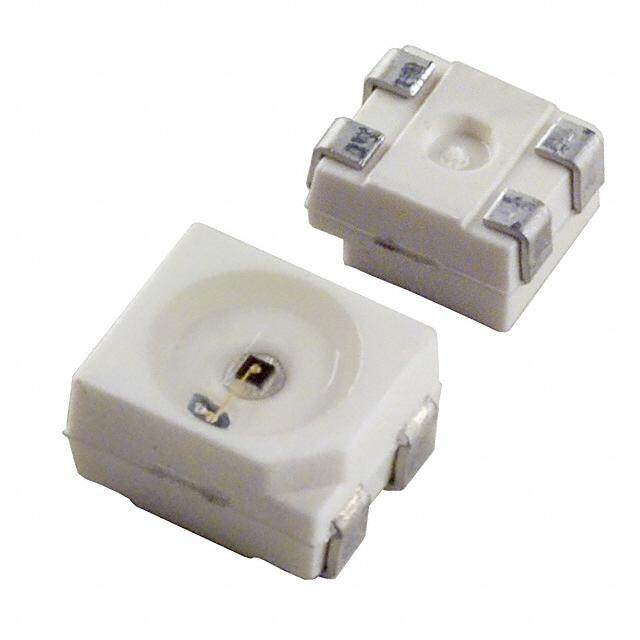
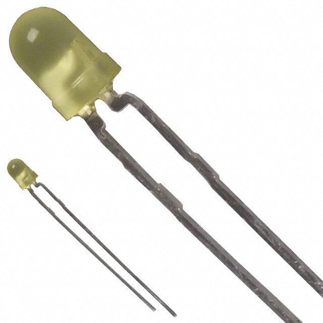
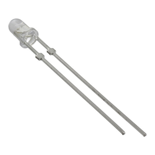
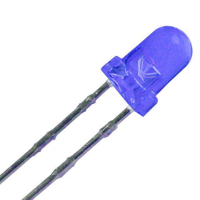
| 描述 | LED RED CLEAR 5MM ROUND标准LED-通孔 Red Clear 624nm |
| 产品分类 | |
| LED大小 | T-1 3/4 |
| 品牌 | Lite-On Inc |
| 产品手册 | |
| 产品图片 |
|
| rohs | 符合RoHS无铅 / 符合限制有害物质指令(RoHS)规范要求 |
| 产品系列 | LED发射器,标准LED-通孔,Lite-On LTL2R3KEK- |
| 数据手册 | |
| 产品型号 | LTL2R3KEK |
| 产品目录绘图 |
|
| 产品目录页面 | |
| 产品种类 | 标准LED-通孔 |
| 光强度 | 700 mcd |
| 其它名称 | 160-1682 |
| 包装 | 散装 |
| 商标 | Lite-On |
| 大小/尺寸 | - |
| 安装类型 | 通孔 |
| 安装风格 | Through Hole |
| 封装 | Bulk |
| 封装/外壳 | 径向 |
| 工厂包装数量 | 1000 |
| 显示角 | 30 deg |
| 最大工作温度 | + 100 C |
| 最小工作温度 | - 40 C |
| 标准包装 | 1,000 |
| 正向电压 | 2.05 V |
| 正向电流 | 20 mA |
| 毫烛光等级 | 700mcd |
| 波长-主 | 624nm |
| 波长-峰值 | 632nm |
| 波长/色温 | 632 nm |
| 测试电流时的光通量 | - |
| 照明颜色 | Red |
| 电压-正向(Vf)(典型值) | 2.05V |
| 电流-测试 | 20mA |
| 视角 | 30° |
| 透镜尺寸 | 5 mm |
| 透镜形状 | Dome |
| 透镜样式/尺寸 | 圆形,带圆顶,5mm,T-1 3/4 |
| 透镜类型 | 透明 |
| 透镜颜色/类型 | Water Clear |
| 颜色 | 红 |
| 高度 | 8.70mm |


PDF Datasheet 数据手册内容提取
Through Hole Lamp Product Data Sheet LTL2R3KEK Spec No.: DS-20-98-0286 Effective Date: 04/18/2015 Revision: C LITE-ON DCC RELEASE BNS-OD-FC001/A4 LITE-ON Technology Corp. / Optoelectronics No.90,Chien 1 Road, Chung Ho, New Taipei City 23585, Taiwan, R.O.C. Tel: 886-2-2222-6181 Fax: 886-2-2221-1948 / 886-2-2221-0660 http://www.liteon.com/opto BBNNSS--OODD--FFCC000011//AA44 BNS-OD-FC001/A4
Through Hole Lamp LTL2R3KEK Through Hole Lamp LTL2R3KEK Rev Description By Date Above data for PD and Customer tracking only C Add Bin Table Spec. Jeromy 04/01/2015 1/9 Part No . : LT L2R3 KEK BNS-OD-FC002/A4
Through Hole Lamp LTL2R3KEK 1. Description Through hole LEDs are offered in a variety of packages such as 3mm, 4mm, 5mm, rectangular, and cylinder which are suitable for all applications requiring status indication. Several intensity and viewing angle choices are available in each color for design flexibility. 1. 1. Features 1.2. Applications High luminous intensity output. Communication Low power consumption. Computer High efficiency. Consumer Versatile mounting on P.C. Board or panel. Home appliance I.C. Compatible/low current requirement. Industrial Popular T-13/4 diameter AlInGaP Red Lamp & Water Clear lens. 2. Outline Dimensions Notes : 1. All dimensions are in millimeters (inches). 2. Tolerance is ±0.25mm (.010") unless otherwise noted. 3. Protruded resin under flange is 1.0mm (.04") max. 4. Lead spacing is measured where the leads emerge from the package. 5. Specifications are subject to change without notice. 2/9 Part No . : LT L2R3 KEK BNS-OD-FC002/A4
Through Hole Lamp LTL2R3KEK 3. Absolute Maximum Ratings at TA=25°C Parameter Maximum Rating Unit Power Dissipation 75 mW Peak Forward Current (1/10 Duty Cycle, 0.1ms Pulse Width) 90 mA DC Forward Current 30 mA Derating Linear From 50°C 0.4 mA/°C Operating Temperature Range -40°C to + 100°C Storage Temperature Range -55°C to + 100°C Lead Soldering Temperature [2.0mm(.0787") From Body] 260°C for 5 Seconds Max. 4. Electrical / Optical Characteristics at TA=25°C Parameter Symbol Min. Typ. Max. Unit Test Condition I = 20mA F Luminous Intensity I 240 700 mcd V Note 1 Viewing Angle 2θ 30 deg Note 2 (Fig.6) 1/2 Measurement Peak Emission Wavelength λ 632 nm P @Peak (Fig.1) Dominant Wavelength λ 624 nm Note 4 d Spectral Line Half-Width Δλ 20 nm Forward Voltage V 2.05 2.4 V I = 20mA F F Reverse Current I 100 μA V = 5V,Note 6 R R NOTE: 1. Luminous intensity is measured with a light sensor and filter combination that approximates the CIE eye-response curve. 2. θ is the off-axis angle at which the luminous intensity is half the axial luminous intensity. 1/2 3. I classification code is marked on each packing bag. v 4. The dominant wavelength, λ is derived from the CIE chromaticity diagram and represents the single wavelength which defines d the color of the device. 5. I guarantee must be included with ±15% testing tolerance. v 6. Reverse voltage (V ) condition is applied for I test only. The device is not designed for reverse operation. R R 3/9 Part No . : LT L2R3 KEK BNS-OD-FC002/A4
Through Hole Lamp LTL2R3KEK 5. Typical Electrical / Optical Characteristics Curves (25°C Ambient Temperature Unless Otherwise Noted) 4/9 Part No . : LT L2R3 KEK BNS-OD-FC002/A4
Through Hole Lamp LTL2R3KEK 6. Packing Spec. 1000, 500 or 200,100 pcs per packing bag 10 packing bags per Inner carton Total 10,000 pcs per Inner carton 8 inner cartons per outer carton Total 80,000 pcs per outer carton In every shipping lot, only the last pack will be non-full packing 5/9 Part No . : LT L2R3 KEK BNS-OD-FC002/A4
Through Hole Lamp LTL2R3KEK 7. Bin Table Specification Luminous Intensity Unit : mcd @20mA Bin Code Min. Max. J 240 310 K 310 400 L 400 520 M 520 680 N 680 880 P 880 1150 Note: Tolerance of each bin limit is ±15% Dominant Wavelength Unit : nm @20mA Bin Code Min Max H28 617.0 621.0 H29 621.0 625.0 H30 625.0 629.0 H31 629.0 633.0 Note: Tolerance of each bin limit is ±1nm 6/9 Part No . : LT L2R3 KEK BNS-OD-FC002/A4
Through Hole Lamp LTL2R3KEK 8. CAUTIONS 8.1. Application This LED lamp is good for application of indoor and outdoor sign, also ordinary electronic equipment. 8.2. Storage The storage ambient for the LEDs should not exceed 30°C temperature or 70% relative humidity. It is recommended that LEDs out of their original packaging are used within three months. For extended storage out of their original packaging, it is recommended that the LEDs be stored in a sealed container with appropriate desiccant or in desiccators with nitrogen ambient. 8.3. Cleaning Use alcohol-based cleaning solvents such as isopropyl alcohol to clean the LEDs if necessary. 8.4. Lead Forming & Assembly During lead forming, the leads should be bent at a point at least 3mm from the base of LED lens. Do not use the base of the lead frame as a fulcrum during forming. Lead forming must be done before soldering, at normal temperature. During assembly on PCB, use minimum clinch force possible to avoid excessive mechanical stress. 8.5. Soldering When soldering, leave a minimum of 2mm clearance from the base of the lens to the soldering point. Dipping the lens into the solder must be avoided. Do not apply any external stress to the lead frame during soldering while the LED is at high temperature. Recommended soldering conditions: Soldering iron Wave soldering Temperature 350°C Max. Pre-heat 100°C Max. Soldering time 3 seconds Max. Pre-heat time 60 seconds Max. (one time only) Solder wave 260°C Max. Position No closer than 2mm Soldering time 5 seconds Max. from the base of the epoxy bulb Dipping Position No lower than 2mm from the base of the epoxy bulb Note: Excessive soldering temperature and/or time might result in deformation of the LED lens or catastrophic failure of the LED. IR reflow is not suitable process for through hole type LED lamp product. 8.6. Drive Method An LED is a current-operated device. In order to ensure intensity uniformity on multiple LEDs connected in parallel in an application, it is recommended that a current limiting resistor be incorporated in the drive circuit, in series with each LED as shown in Circuit A below. Circuit model (A) Circuit model (B) LED LED (A) Recommended circuit (B) The brightness of each LED might appear different due to the differences in the I-V characteristics of those LEDs. 7/9 Part No . : LT L2R3 KEK BNS-OD-FC002/A4
Through Hole Lamp LTL2R3KEK 8.7. ESD (Electrostatic Discharge) Static Electricity or power surge will damage the LED. Suggestions to prevent ESD damage: Use a conductive wrist band or anti- electrostatic glove when handling these LEDs All devices, equipment, and machinery must be properly grounded Work tables, storage racks, etc. should be properly grounded Use ion blower to neutralize the static charge which might have built up on surface of the LEDs plastic lens as a result of friction between LEDs during storage and handing Suggested checking list: Training and Certification 8.7.1.1. Everyone working in a static-safe area is ESD-certified? 8.7.1.2. Training records kept and re-certification dates monitored? Static-Safe Workstation & Work Areas 8.7.2.1. Static-safe workstation or work-areas have ESD signs? 8.7.2.2. All surfaces and objects at all static-safe workstation and within 1 ft measure less than 100V? 8.7.2.3. All ionizer activated, positioned towards the units? 8.7.2.4. Each work surface mats grounding is good? Personnel Grounding 8.7.3.1. Every person (including visitors) handling ESD sensitive (ESDS) items wear wrist strap, heel strap or conductive shoes with conductive flooring? 8.7.3.2. If conductive footwear used, conductive flooring also present where operator stand or walk? 8.7.3.3. Garments, hairs or anything closer than 1 ft to ESD items measure less than 100V*? 8.7.3.4. Every wrist strap or heel strap/conductive shoes checked daily and result recorded for all DLs? 8.7.3.5. All wrist strap or heel strap checkers calibration up to date? Note: *50V for Blue LED. Device Handling 8.7.4.1. Every ESDS items identified by EIA-471 labels on item or packaging? 8.7.4.2. All ESDS items completely inside properly closed static-shielding containers when not at static-safe workstation? 8.7.4.3. No static charge generators (e.g. plastics) inside shielding containers with ESDS items? 8.7.4.4. All flexible conductive and dissipative package materials inspected before reuse or recycle? Others 8.7.5.1. Audit result reported to entity ESD control coordinator? 8.7.5.2. Corrective action from previous audits completed? 8.7.5.3. Are audit records complete and on file? 8/9 Part No . : LT L2R3 KEK BNS-OD-FC002/A4
Through Hole Lamp LTL2R3KEK 9. Reliability Test Classification Test Item Test Condition Sample Size Reference Standard Ta = Under room temperature 22 PCS IF = per datasheet maximum drive MIL-STD-750D:1026 (1995) Operation Life (CL=90%; current MIL-STD-883G:1005 (2006) LTPD=10%) Test Time= 1000hrs High Temperature Ta = 60°C 22 PCS MIL-STD-202G:103B (2002) High Humidity RH = 90% (CL=90%; JEITA ED-4701:100 103 (2001) storage Test Time= 240hrs LTPD=10%) Endurance Test 22 PCS MIL-STD-750D:1031 (1995) High Temperature Ta= 105 ± 5°C (CL=90%; MIL-STD-883G:1008 (2006) Storage Test Time= 1000hrs LTPD=10%) JEITA ED-4701:200 201 (2001) 22 PCS Low Temperature Ta= -55 ± 5°C (CL=90%; JEITA ED-4701:200 202 (2001) Storage Test Time= 1000hrs LTPD=10%) MIL-STD-750D:1051 (1995) 100°C ~ 25°C ~ -40°C ~ 25°C 22 PCS Temperature MIL-STD-883G:1010 (2006) 30mins 5mins 30mins 5mins (C L=90%; Cycling JEITA ED-4701:100 105 (2001) 30 Cycles LTPD=10%) JESD22-A104C (2005) 100 ± 5°C ~ -30°C ± 5°C MIL-STD-750D:1056 (1995) 22 PCS Thermal 15mins 15mins MIL-STD-883G:1011 (2006) (CL=90%; Shock 30 Cycles MIL-STD-202G:107G (2002) LTPD=10%) (<20 secs transfer) JESD22-A106B (2004) Environmental T.sol = 260 ± 5°C 11 PCS Solder MIL-STD-750D:2031(1995) Dwell Time= 10±1 seconds (CL=90%; Test Resistance JEITA ED-4701: 300 302 (2001) 3mm from the base of the epoxy bulb LTPD=18.9%) T. sol = 245 ± 5°C MIL-STD-750D:2026 (1995) 11 PCS Dwell Time= 5 ± 0.5 seconds MIL-STD-883G:2003 (2006) Solderability (CL=90%; (Lead Free Solder, Coverage ≧95% of MIL-STD-202G:208H (2002) LTPD=18.9%) the dipped surface) IPC/EIA J-STD-002 (2004) 11 PCS T. sol = 350 ± 5°C MIL-STD-202G:208H (2002) Soldering Iron (CL=90%; Dwell Time= 3.5 ± 0.5 seconds JEITA ED-4701:300 302 (2001) LTPD=18.9%) 10. Others The appearance and specifications of the product may be modified for improvement, without prior notice. 9/9 Part No . : LT L2R3 KEK BNS-OD-FC002/A4
Mouser Electronics Authorized Distributor Click to View Pricing, Inventory, Delivery & Lifecycle Information: L ite-On: LTL2R3KEK