ICGOO在线商城 > 集成电路(IC) > PMIC - 稳压器 - DC DC 切换控制器 > LTC3862HFE#PBF
/LTC3862HFE#PBF.jpg)
 Datasheet下载
- 型号: LTC3862HFE#PBF
- 制造商: LINEAR TECHNOLOGY
- 库位|库存: xxxx|xxxx
- 要求:
| 数量阶梯 | 香港交货 | 国内含税 |
| +xxxx | $xxxx | ¥xxxx |
查看当月历史价格
查看今年历史价格
LTC3862HFE#PBF产品简介:
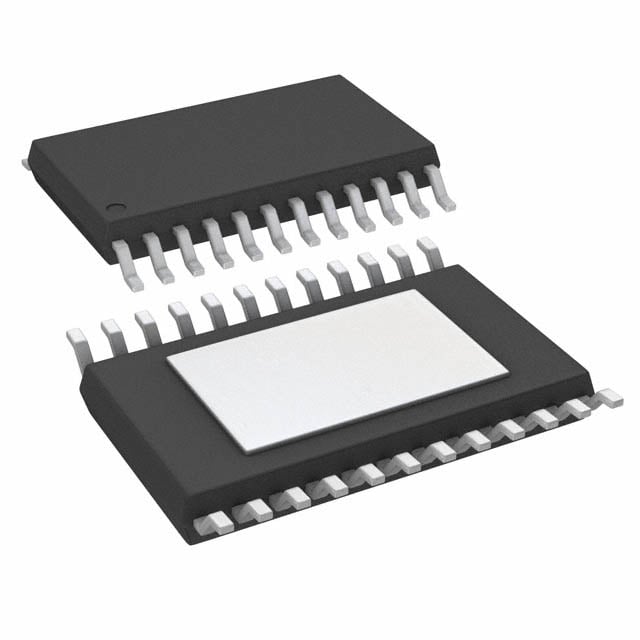
ICGOO电子元器件商城为您提供LTC3862HFE#PBF由LINEAR TECHNOLOGY设计生产,在icgoo商城现货销售,并且可以通过原厂、代理商等渠道进行代购。 LTC3862HFE#PBF价格参考。LINEAR TECHNOLOGYLTC3862HFE#PBF封装/规格:PMIC - 稳压器 - DC DC 切换控制器, 升压,SEPIC 稳压器 正 输出 升压,升压/降压 DC-DC 控制器 IC 24-TSSOP-EP。您可以下载LTC3862HFE#PBF参考资料、Datasheet数据手册功能说明书,资料中有LTC3862HFE#PBF 详细功能的应用电路图电压和使用方法及教程。
| 参数 | 数值 |
| 产品目录 | 集成电路 (IC) |
| Cuk | 无 |
| 描述 | IC REG CTRLR BST PWM CM 24-TSSOP |
| 产品分类 | |
| 品牌 | Linear Technology |
| 数据手册 | http://www.linear.com/docs/26473 |
| 产品图片 |
|
| 产品型号 | LTC3862HFE#PBF |
| PWM类型 | 电流模式 |
| rohs | 无铅 / 符合限制有害物质指令(RoHS)规范要求 |
| 产品系列 | - |
| 倍增器 | 无 |
| 其它名称 | LTC3862HFEPBF |
| 分频器 | 无 |
| 包装 | 管件 |
| 升压 | 是 |
| 占空比 | 96% |
| 反向 | 无 |
| 反激式 | 无 |
| 封装/外壳 | 24-TSSOP(0.173",4.40mm 宽)裸焊盘 |
| 工作温度 | -40°C ~ 150°C |
| 标准包装 | 62 |
| 电压-电源 | 4 V ~ 36 V |
| 输出数 | 1 |
| 配用 | /product-detail/zh/DC1891A/DC1891A-ND/4866617 |
| 降压 | 无 |
| 隔离式 | 无 |
| 频率-最大值 | 500kHz |


- 商务部:美国ITC正式对集成电路等产品启动337调查
- 曝三星4nm工艺存在良率问题 高通将骁龙8 Gen1或转产台积电
- 太阳诱电将投资9.5亿元在常州建新厂生产MLCC 预计2023年完工
- 英特尔发布欧洲新工厂建设计划 深化IDM 2.0 战略
- 台积电先进制程称霸业界 有大客户加持明年业绩稳了
- 达到5530亿美元!SIA预计今年全球半导体销售额将创下新高
- 英特尔拟将自动驾驶子公司Mobileye上市 估值或超500亿美元
- 三星加码芯片和SET,合并消费电子和移动部门,撤换高东真等 CEO
- 三星电子宣布重大人事变动 还合并消费电子和移动部门
- 海关总署:前11个月进口集成电路产品价值2.52万亿元 增长14.8%


PDF Datasheet 数据手册内容提取
LTC3862 Multi-Phase Current Mode Step-Up DC/DC Controller FeaTures DescripTion n Wide V Range: 4V to 36V Operation The LTC®3862 is a two phase constant frequency, current IN n 2-Phase Operation Reduces Input and Output mode boost and SEPIC controller that drives N-channel Capacitance power MOSFETs. Two phase operation reduces system n Fixed Frequency, Peak Current Mode Control filtering capacitance and inductance requirements. n 5V Gate Drive for Logic-Level MOSFETs The operating frequency can be set with an external resistor n Adjustable Slope Compensation Gain over a 75kHz to 500kHz range and can be synchronized n Adjustable Max Duty Cycle (Up to 96%) to an external clock using the internal PLL. Multi-phase n Adjustable Leading Edge Blanking operation is possible using the SYNC input, the CLKOUT n ±1% Internal Voltage Reference output and the PHASEMODE control pin allowing 2-, 3-, n Programmable Operating Frequency with One 4-, 6- or 12-phase operation. External Resistor (75kHz to 500kHz) n Phase-Lockable Fixed Frequency 50kHz to 650kHz Other features include an internal 5V LDO with undervoltage n SYNC Input and CLKOUT for 2-, 3-, 4-, 6- or lockout protection for the gate drivers, a precision RUN 12-Phase Operation (PHASEMODE Programmable) pin threshold with programmable hysteresis, soft-start n Internal 5V LDO Regulator and programmable leading edge blanking and maximum n 24-Lead Narrow SSOP Package duty cycle. n 5mm × 5mm QFN with 0.65mm Lead Pitch and PART NUMBER INTV V ON V OFF CC IN IN 24-Lead Thermally Enhanced TSSOP Packages LTC3862 5V 3.3V 2.9V applicaTions LTC3862-1 10V 7.5V 7.0V LTC3862-2 10V 4.4V 3.9V n Automotive, Telecom and Industrial Power Supplies L, LT, LTC, LTM, Linear Technology and the Linear logo are registered trademarks of Linear Technology Corporation. All other trademarks are the property of their respective owners. Protected by U.S. Patents, including 6144194, 6498466, 6611131. Typical applicaTion VIN 5V TO 36V 22µF 84.5k 19.4µH 19.4µH 50V VOUT 48V Efficiency vs Output Current 24.9k VIN 5A (MAX) RUN GATE1 98 INTVCC SENSE1+ VOUT = 48V 220µF 96 VIN = 12V 4.7µF LTC3862 0.006Ω 50V 94 66.5k BLANK SENSE1– FREQ GATE2 %) 92 10nF1n1F0k10nF SSPYLSLNFCLTR SSEENNSSEE22+– 0.006Ω EFFICIENCY ( 889860 VIVNI N= =5 V24V 3V8 PGND 84 CLKOUT FB SLOPE 82 10nF DMAX 80 ITH PHASEMODE 100 1000 10000 475k 12.4k 68.1k 100pF SGND LOAD CURRENT (mA) 3862 TA01b 3862 TA01 3862fc 1 For more information www.linear.com/LTC3862
LTC3862 absoluTe MaxiMuM raTings (Notes 1, 2) Input Supply Voltage (V ) .........................–0.3V to 40V ITH Voltage ...............................................–0.3V to 2.7V IN INTV Voltage ............................................–0.3V to 6V FB Voltage .................................................–0.3V to V CC 3V8 INTV LDO RMS Output Current .........................50mA FREQ Voltage ............................................–0.3V to 1.5V CC RUN Voltage ................................................–0.3V to 8V Operating Junction Temperature Range (Notes 3, 4) SYNC Voltage ...............................................–0.3V to 6V LTC3862E .............................................–40°C to 85°C SLOPE, PHASEMODE, D , LTC3862I............................................–40°C to 125°C MAX BLANK Voltage ..........................................–0.3V to V LTC3862H ..........................................–40°C to 150°C 3V8 SENSE1+, SENSE1–, SENSE2+, Storage Temperature Range ...................–65°C to 150°C SENSE2– Voltage ......................................–0.3V to V Reflow Peak Body Temperature ...........................260°C 3V8 SS, PLLFLTR Voltage ................................–0.3V to V 3V8 pin conFiguraTion TOP VIEW TOP VIEW TOP VIEW SDLOMPAEX 12 2243 3SVE8NSE1+ SDLOMPAEX 12 2243 3SVE8NSE1+ SLOPE DMAX 3V8+SENSE1–SENSE1 RUN BLANK 3 22 SENSE1– BLANK 3 22 SENSE1– 24 23 22 21 20 19 PHASEMODE 4 21 RUN PHASEMODE 4 21 RUN BLANK 1 18 VIN FREQ 5 20 VIN FREQ 5 20 VIN PHASEMODE 2 17 INTVCC SS 6 25 19 INTVCC SS 6 19 INTVCC FREQ 3 25 16 GATE1 ITH 7 18 GATE1 SS 4 15 PGND ITH 7 18 GATE1 FB 8 17 PGND ITH 5 14 GATE2 FB 8 17 PGND SGND 9 16 GATE2 FB 6 13 NC SGND 9 16 GATE2 CLKOUT 10 15 NC 7 8 9 10 11 12 CLKOUT 10 15 NC PLLSFYLNTRC 1112 1143 SSEENNSSEE22–+ PLLSFYLNTRC 1112 1143 SSEENNSSEE22–+ SGND CLKOUT SYNC PLLFLTR+SENSE2–SENSE2 FE PACKAGE UH PACKAGE 24-LEAD PLASTIC TSSOP 24-LEAD NGANR RPOAWCK PALGAESTIC SSOP 24-LEAD (5mm × 5mm) PLASTIC QFN EXPOSED PAD (PTINJM 2A5X) =IS 1 5P0G°NCD, ,θ MJAU =S 3T8 B°CE /SWO LDERED TO PCB TJMAX = 150°C, θJA = 85°C/W EXPOSED PAD (PTINJM 2A5X) =IS 1 5P0G°NCD, ,θ MJAU =S 4T4 B°CE /SWO LDERED TO PCB orDer inForMaTion LEAD FREE FINISH TAPE AND REEL PART MARKING* PACKAGE DESCRIPTION TEMPERATURE RANGE LTC3862EFE#PBF LTC3862EFE#TRPBF 3862FE 24-Lead Plastic TSSOP –40°C to 85°C LTC3862IFE#PBF LTC3862IFE#TRPBF 3862FE 24-Lead Plastic TSSOP –40°C to 125°C LTC3862HFE#PBF LTC3862HFE#TRPBF 3862FE 24-Lead Plastic TSSOP –40°C to 150°C LTC3862EGN#PBF LTC3862EGN#TRPBF LTC3862GN 24-Lead Plastic SSOP –40°C to 85°C LTC3862IGN#PBF LTC3862IGN#TRPBF LTC3862GN 24-Lead Plastic SSOP –40°C to 125°C LTC3862HGN#PBF LTC3862HGN#TRPBF LTC3862GN 24-Lead Plastic SSOP –40°C to 150°C LTC3862EUH#PBF LTC3862EUH#TRPBF 3862 24-Lead (5mm × 5mm) Plastic QFN –40°C to 85°C LTC3862IUH#PBF LTC3862IUH#TRPBF 3862 24-Lead (5mm × 5mm) Plastic QFN –40°C to 125°C LTC3862HUH#PBF LTC3862HUH#TRPBF 3862 24-Lead (5mm × 5mm) Plastic QFN –40°C to 150°C Consult LTC Marketing for parts specified with wider operating temperature ranges. *The temperature grade is identified by a label on the shipping container. Consult LTC Marketing for information on non-standard lead based finish parts. For more information on lead free part marking, go to: http://www.linear.com/leadfree/ For more information on tape and reel specifications, go to: http://www.linear.com/tapeandreel/ 3862fc 2 For more information www.linear.com/LTC3862
LTC3862 elecTrical characTerisTics (Notes 2, 3) The l denotes the specifications which apply over the specified operating junction temperature range, otherwise specifications are at T = 25°C. V = 12V, RUN = 2V and SS = open, unless A IN otherwise noted. SYMBOL PARAMETER CONDITIONS MIN TYP MAX UNITS Supply Input and INTV Linear Regulator CC V V Supply Voltage Range 4 36 V IN IN I V Supply Current VIN IN Normal Mode, No Switching (Note 5) l 1.8 3.0 mA Shutdown V = 0V l 30 80 µA RUN INTV LDO Regulator Output Voltage 4.8 5.0 5.2 V CC dV Line Regulation 6V < V < 36V 0.002 0.02 %/V INTVCC(LINE) IN dV Load Regulation Load = 0mA to 20mA –2 % INTVCC(LOAD) V INTV UV+ Voltage Rising INTV 3.3 V UVLO CC CC INTV UV– Voltage Falling INTV 2.9 V CC CC 3V8 LDO Regulator Output Voltage 3.8 V Switcher Control Loop V Reference Voltage V = 0.8V (Note 6) E-Grade (Note 3) l 1.210 1.223 1.235 V FB ITH I-Grade and H-Grade (Note 3) l 1.199 1.223 1.248 V dV /dV Feedback Voltage V Line Regulation V = 4V to 36V (Note 6) ±0.002 0.01 %/V FB IN IN IN dV /dV Feedback Voltage Load Regulation V = 0.5V to 1.2V (Note 6) 0.01 0.1 % FB ITH ITH g Transconductance Amplifier Gain V = 0.8V (Note 6), ITH Pin Load = ±5µA 660 µMho m ITH f Error Amplifier Unity-Gain Crossover (Note 7) 1.8 MHz 0dB Frequency V Error Amplifier Maximum Output Voltage V = 1V, No Load 2.7 V ITH FB (Internally Clamped) Error Amplifier Minimum Output Voltage V = 1.5V, No Load 50 mV FB I Error Amplifier Output Source Current –30 µA ITH Error Amplifier Output Sink Current 30 µA I Error Amplifier Input Bias Currents (Note 6) –50 –200 nA FB V Pulse Skip Mode Operation ITH Pin Voltage Rising ITH Voltage (Note 6) 0.275 V ITH(PSKIP) Hysteresis 25 mV I SENSE Pin Current 0.01 2 µA SENSE(ON) V Maximum Current Sense Input Threshold V = Float, Low Duty Cycle 65 75 85 mV SENSE(MAX) SLOPE (Note 3) l 60 75 90 mV V CH1 to CH2 Maximum Current Sense V = Float, Low Duty Cycle (Note 3) l –10 10 mV SENSE(MATCH) SLOPE Threshold Matching (V – V ) SENSE1 SENSE2 RUN/Soft-Start I RUN Source Current V = 0V –0.5 µA RUN RUN V = 1.5V –5 µA RUN V High Level RUN Channel Enable Threshold 1.22 V RUN V RUN Threshold Hysteresis 80 mV RUNHYS I SS Pull-Up Current V = 0V –5 µA SS SS R SS Pull-Down Resistance V = 0V 10 kΩ SS RUN Oscillator f Oscillator Frequency R = 45.6k 280 300 320 kHz OSC FREQ R = 45.6k l 260 300 340 kHz FREQ Oscillator Frequency Range l 75 500 kHz V Nominal FREQ Pin Voltage R = 45.6k 1.223 V FREQ FREQ 3862fc 3 For more information www.linear.com/LTC3862
LTC3862 elecTrical characTerisTics (Notes 2, 3) The l denotes the specifications which apply over the specified operating junction temperature range, otherwise specifications are at T = 25°C. V = 12V, RUN = 2V and SS = open, unless A IN otherwise noted. SYMBOL PARAMETER CONDITIONS MIN TYP MAX UNITS f SYNC Minimum Input Frequency V = External Clock l 50 kHz SYNC SYNC SYNC Maximum Input Frequency V = External Clock l 650 kHz SYNC V SYNC Input Threshold Rising Threshold 1.5 V SYNC I Phase Detector Sourcing Output Current f > f –15 µA PLLFLTR SYNC OSC Phase Detector Sinking Output Current f < f 15 µA SYNC OSC CH1-CH2 Channel 1 to Channel 2 Phase Relationship V = 0V 180 Deg PHASEMODE V = Float 180 Deg PHASEMODE V = 3V8 120 Deg PHASEMODE CH1-CLKOUT Channel 1 to CLKOUT Phase Relationship V = 0V 90 Deg PHASEMODE V = Float 60 Deg PHASEMODE V = 3V8 240 Deg PHASEMODE D Maximum Duty Cycle V = 0V (Note 9) 96 % MAX DMAX V = Float 84 % DMAX V = 3V8 75 % DMAX t Minimum On-Time V = 0V (Note 8) 180 ns ON(MIN)1 BLANK t Minimum On-Time V = Float (Note 8) 260 ns ON(MIN)2 BLANK t Minimum On-Time V = 3V8 (Note 8) 340 ns ON(MIN)3 BLANK Gate Driver R Driver Pull-Up R 2.1 Ω DS(ON) DS(ON) Driver Pull-Down R 0.7 Ω DS(ON) Overvoltage V V , Overvoltage Lockout Threshold V – V in Percent 8 10 12 % FB(OV) FB FB(OV) FB(NOM) Note 1: Stresses beyond those listed under Absolute Maximum Ratings Note 4: This IC includes overtemperature protection that is intended to may cause permanent damage to the device. Exposure to any Absolute protect the device during momentary overload conditions. Continuous Maximum Rating condition for extended periods may affect device operation above the specified maximum operating junction temperature reliability and lifetime. may impair device reliability. Note 2: All currents into device pins are positive; all currents out of device Note 5: Supply current in normal operation is dominated by the current pins are negative. All voltages are referenced to ground unless otherwise needed to charge the external MOSFET gates. This current will vary with specified. supply voltage and the external MOSFETs used. Note 3: The LTC3862E is guaranteed to meet performance specifications Note 6: The IC is tested in a feedback loop that adjusts V to achieve a FB from 0°C to 85°C. Specifications over the –40°C to 85°C operating specified error amplifier output voltage. junction temperature range are assured by design, characterization and Note 7: Guaranteed by design, not subject to test. correlation with statistical process controls. The LTC3862I is guaranteed Note 8: The minimum on-time condition is specified for an inductor peak- over the full –40°C to 125°C operating junction temperature range and to-peak ripple current = 30% (see Minimum On-Time Considerations in the the LTC3862H is guaranteed over the full –40°C to 150°C operating Applications Information section). junction temperature range. High junction temperatures degrade operating Note 9: The maximum duty cycle limit is derived from an internal lifetimes. Operating lifetime is derated at junction temperatures greater clock that runs at 12x the programmed switching frequency. See the than 125°C. Applications Information for additional information. 3862fc 4 For more information www.linear.com/LTC3862
LTC3862 Typical perForMance characTerisTics Efficiency and Power Loss vs Efficiency vs Output Current Input Voltage 100 96 4000 VOUT = 48V 95 EFFICIENCY 95 90 3500 %) 85 VIN = 35V %) 94 POW CY ( 80 CY ( 3000ER L EFFICIEN 7705 VIN = 24V EFFICIEN 9923 POWER LOSS 2500OSS (mW 65 ) VIN = 12V 60 2000 91 55 VOUT = 48V IOUT = 1A 50 90 1500 10 100 1000 10000 0 10 20 30 40 LOAD CURRENT (mA) INPUT VOLTAGE (V) 3862 G01 3862 G02 Quiescent Current vs Input Load Step Inductor Current at Light Load Voltage 3.00 ILOAD 2.75 5A/DIV SW1 1A TO 5A 50V/DIV 2.50 5A/DILIV1 50VS/DWIV2 RENT (mA)221...207505 R IL2 U1.50 5A/DIV 2A/DILIV1 NT C1.25 E VOUT IL2 SC1.00 500mV/DIV 2A/DIV UIE0.75 Q VIN = 24V 500µs/DIV 3862 G03 VIN = 12V 1µs/DIV 3862 G04 0.50 VOUT = 48V VOUT = 48V 0.25 ILOAD = 100mA 0 4 8 12 16 20 24 28 32 36 INPUT VOLTAGE (V) 3862 G05 Shutdown Quiescent Current vs Shutdown Quiescent Current vs Quiescent Current vs Temperature Input Voltage Temperature 1.90 45 50 VIN = 12V 1.85 40 QUIESCENT CURRENT (mA)11111.....7866700055 SHUTDOWN CURRENT (µA) 323112005505 SHUTDOWN CURRENT (µA) 42130000 1.55 5 1.50 0 0 –50 –25 0 25 50 75 100 125 150 4 8 12 16 20 24 28 32 36 –50 –25 0 25 50 75 100 125 150 TEMPERATURE (°C) INPUT VOLTAGE (V) TEMPERATURE (°C) 3862 G06 3862 G07 3862 G08 3862fc 5 For more information www.linear.com/LTC3862
LTC3862 Typical perForMance characTerisTics INTV Line Regulation INTV Load Regulation INTV vs Temperature CC CC CC 5.25 5.00 5.00 4.99 4.98 4.95 GE (V) GE (V) GE (V) 44..9967 OLTA5.00 OLTA4.90 OLTA 4.95 V V V V CC V CC V CC4.94 NT NT NT 4.93 I I4.85 I 4.92 4.91 4.75 4.80 4.90 0 5 10 15 20 25 0 10 20 30 40 50 –50 –25 0 25 50 75 100 125 150 INPUT VOLTAGE (V) INTVCC LOAD CURRENT (mA) TEMPERATURE (°C) 3962 G09 3862 G10 3862 G11 INTV LDO Dropout vs Load INTV UVLO Threshold vs CC CC Current, Temperature Temperature Feedback Voltage vs Temperature 1600 3.6 1.235 3.5 1.233 1400 150°C 1.231 3.4 V)1200 1.229 POUT VOLTAGE (m1860000000 125°C 8255°°CC TV VOLTAGE (V)CC 3333....2013 FB VOLTAGE (V)11111.....222221222293715 O N 2.9 DR 400 –40°C I 1.217 2.8 1.215 200 2.7 1.213 0 2.6 1.211 0 10 20 30 40 50 –50 –25 0 25 50 75 100 125 150 –50 –25 0 25 50 75 100 125 150 INTVCC LOAD (mA) TEMPERATURE (°C) TEMPERATURE (°C) 3862 G12 3862 G13 3862 G14 Feedback Voltage Line Current Sense Threshold vs Current Sense Threshold vs Regulation ITH Voltage Temperature 1.226 80 80 79 FB VOLTAGE (V)11111.....222222222231452 CURRENT SENSE THRESHOLD (mV) 56734210000000 CURRENT SENSE THRESHOLD (mV) 7777777763457281 1.220 0 70 4 8 12 16 20 24 28 32 36 0 0.4 0.8 1.2 1.6 2.0 2.4 –50 –25 0 25 50 75 100 125 150 INPUT VOLTAGE (V) ITH VOLTAGE (V) TEMPERATURE (°C) 3862 G15 3862 G16 3862 G17 3862fc 6 For more information www.linear.com/LTC3862
LTC3862 Typical perForMance characTerisTics Maximum Current Sense Threshold vs Duty Cycle RUN Threshold vs Temperature RUN Threshold vs Input Voltage V) 80 1.30 1.5 m LD ( 75 SLOPE = 0.625 HO ON 1.4 ENSE THRES 7605 SSLOLOPPE E= =1 1.66 OLTAGE (V)11..2250 OLTAGE (V) 1.3 ON S V V RRENT 60 UN PIN OFF UN PIN 1.2 OFF CU R1.15 R M 1.1 U 55 M XI A M 50 1.10 1.0 0 10 20 30 40 50 60 70 80 90 100 –50 –25 0 25 50 75 100 125 150 0 5 10 15 20 25 30 35 40 DUTY CYCLE (%) TEMPERATURE (°C) INPUT VOLTAGE (V) 3862 G18 3862 G09 3862 G20 RUN (Off) Source Current vs RUN (On) Source Current vs RUN Source Current vs Temperature Temperature Input Voltage 0 0 0 –0.1 –1 –1 –0.2 RUN PIN CURRENT (µA)–––––00000.....47653 RUN PIN CURRENT (µA) –––––42653 RUN PIN CURRENT (µA) ––––3452 –0.8 –0.9 –7 –6 –1.0 –8 –7 –50 –25 0 25 50 75 100 125 150 –50 –25 0 25 50 75 100 125 150 4 8 12 16 20 24 28 32 36 TEMPERATURE (°C) TEMPERATURE (°C) INPUT VOLTAGE (V) 3862 G21vv 1344 G06 3862 G23 Soft-Start Current vs Oscillator Frequency vs Soft-Start Current vs Temperature Soft-Start Voltage Temperature –5.0 0 307 306 –5.1 –1 A) A) 305 µ µ CURRENT (––55..32 CURRENT ( ––32 NCY (kHz) 330034 RT RT UE 302 A A Q T T E T-S–5.4 T-S –4 FR 301 F F O O S S 300 –5.5 –5 299 –5.6 –6 298 –50 –25 0 25 50 75 100 125 150 0 0.5 1 1.5 2 2.5 3 3.5 4 –50 –25 0 25 50 75 100 125 150 TEMPERATURE (°C) SOFT-START VOLTAGE (V) TEMPERATURE (°C) 3862 G24 3862 G25 3862 G26 3862fc 7 For more information www.linear.com/LTC3862
LTC3862 Typical perForMance characTerisTics Oscillator Frequency vs Input Voltage R vs Frequency Frequency vs PLLFLTR Voltage FREQ 320 1000 1400 315 1200 310 REQUENCY (kHz) 323090550 R (kΩ)FREQ100 REQUENCY (kHz)1860000000 F F 400 290 285 200 280 10 0 0 4 8 12 16 20 24 28 32 36 0 100 200300 400500600700800 9001000 0 0.5 1 1.5 2 2.5 INPUT VOLTAGE (V) FREQUENCY (kHz) PLLFLTR VOLTAGE (V) 3862 G27 3862 G28 3862 G29 Frequency Voltage vs Minimum On-Time vs Minimum On-Time vs Temperature Temperature Input Voltage 1.235 400 400 1.233 1.231 350 BLANK = 3V8 350 BLANK = 3V8 E (V)11..222297 ME (ns)300 ME (ns)300 Q VOLTAG111...222222513 UM ON-TI250 BLANK = FLOAT UM ON-TI250 BLANK = FLOAT E M M FR11..221197 MINI200 BLANK = SGND MINI200 BLANK = SGND 1.215 150 150 1.213 1.211 100 100 –50 –25 0 25 50 75 100 125 150 –50 –25 0 25 50 75 100 125 150 4 8 12 16 20 24 28 32 36 TEMPERATURE (°C) TEMPERATURE (°C) INPUT VOLTAGE (V) 3862 G30 3862 G31 3862 G32 Gate Turn-On Waveform Driving Gate Turn-Off Waveform Driving Renesas HAT2266 Renesas HAT2266 GATE GATE 1V/DIV 1V/DIV VIN = 12V 20ns/DIV 3862 G33 VIN = 12V 20ns/DIV 3862 G34 VOUT = 48V VOUT = 48V IOUT = 1A IOUT = 1A MOSFET RENESAS HAT2266 MOSFET RENESAS HAT2266 3862fc 8 For more information www.linear.com/LTC3862
LTC3862 pin FuncTions (SSOP/QFN/TSSOP) 3V8 (Pin 24/Pin 22/Pin 24): Output of the Internal 3.8V INTV (Pin 19/Pin 17/Pin 19): Output of the Internal 5V CC LDO from INTV . Supply pin for the low voltage analog Low Dropout Regulator (LDO). A low ESR 4.7µF (X5R or CC and digital circuits. A low ESR 1nF ceramic bypass capacitor better) ceramic bypass capacitor should be connected should be connected between 3V8 and SGND, as close between INTV and PGND, as close as possible to the IC. CC as possible to the IC. ITH (Pin 7/Pin 5/Pin 7): Error Amplifier Output. The current BLANK (Pin 3/Pin 1/Pin 3): Blanking Time. Floating this comparator trip threshold increases with the ITH control pin provides a nominal minimum on-time of 260ns. Con- voltage. The ITH pin is also used for compensating the necting this pin to 3V8 provides a minimum on-time of control loop of the converter. 340ns, while connecting it to SGND provides a minimum PGND (Pin 17/Pin 15, Exposed Pad Pin 25/Pin 17, on-time of 180ns. Exposed Pad Pin 25): Power Ground. Connect this pin CLKOUT (Pin 10/Pin 8/Pin 10): Digital Output Used for close to the sources of the power MOSFETs. PGND should Daisy-Chaining Multiple LTC3862 ICs in Multi-Phase also be connected to the negative terminals of V and IN Systems. The PHASEMODE pin voltage controls the INTV bypass capacitors. PGND is electrically isolated CC relationship between CH1 and CH2 as well as between from the SGND pin. The Exposed Pad of the FE and QFN CH1 and CLKOUT. packages is connected to PGND and must be soldered to PCB ground for electrical contact and rated thermal D (Pin 1/Pin 23/Pin 1): Maximum Duty Cycle. This pin MAX performance. programs the maximum duty cycle. Floating this pin pro- vides 84% duty cycle. Connecting this pin to 3V8 provides PHASEMODE (Pin 4/Pin 2/Pin 4): The PHASEMODE pin 75% duty cycle, while connecting it to SGND provides 96% voltage programs the phase relationship between CH1 and duty cycle. The maximum duty cycle is derived from an CH2 rising gate signals, as well as the phase relationship internal clock that runs at 12x the programmed switching between CH1 gate signal and CLKOUT. Floating this pin or frequency. As a result, the maximum duty cycle limit D connecting it to either 3V8, or SGND changes the phase MAX is extremely precise. relationship between CH1, CH2 and CLKOUT. FB (Pin 8/Pin 6/Pin 8): Error Amplifier Input. The FB pin PLLFLTR (Pin 12/Pin 10/Pin 12): PLL Lowpass Filter Input. should be connected through a resistive divider network When synchronizing to an external clock, this pin serves as to V to set the output voltage. the lowpass filter input for the PLL. A series resistor and OUT capacitor connected from PLLFLTR to SGND compensate FREQ (Pin 5/Pin 3/Pin 5): A resistor from FREQ to SGND the PLL feedback loop. sets the operating frequency. RUN (Pin 21/Pin 19/Pin 21): Run Control Input. A voltage GATE1 (Pin 18/Pin 16/Pin 18): Gate Drive Output. The above 1.22V on the pin turns on the IC. Forcing the pin LTC3862 provides a 5V gate drive referenced to PGND to below 1.22V causes the IC to shut down. There is a 0.5µA drive a logic-level threshold MOSFET. The gate pin is rated pull-up current for this pin. Once the RUN pin raises above for an absolute maximum voltage of –0.3V minimum and 1.22V, an additional 4.5µA pull-up current is added to the 6V maximum. pin for programmable hysteresis. GATE2 (Pin 16/Pin 14/Pin 16): Gate Drive Output. The SENSE1+ (Pin 23/Pin 21/Pin 23): Positive Inputs to the LTC3862 provides a 5V gate drive referenced to PGND to Current Comparators. The ITH pin voltage programs the drive a logic-level threshold MOSFET. The gate pin is rated current comparator offset in order to set the peak current for an absolute maximum voltage of –0.3V minimum and trip threshold. This pin is normally connected to a sense 6V maximum. resistor in the source of the power MOSFET. 3862fc 9 For more information www.linear.com/LTC3862
LTC3862 pin FuncTions (SSOP/QFN/TSSOP) SENSE2+ (Pin 13/Pin 11/Pin 13): Positive Inputs to the slope compensation by 66%, and connecting it to SGND Current Comparators. The ITH pin voltage programs the decreases the normalized slope compensation by 37.5%. current comparator offset in order to set the peak current See Applications Information for more details. trip threshold. This pin is normally connected to a sense SS (Pin 6/Pin 4/Pin 6): Soft-Start Input. For soft-start resistor in the source of the power MOSFET. operation, connecting a capacitor from this pin to SGND SENSE1– (Pin 22/Pin 20/Pin 22): Negative Inputs to the will clamp the output of the error amp. An internal 5µA Current Comparators. This pin is normally connected to current source will charge the capacitor and set the rate the bottom of the sense resistor. of increase of the peak switch current of the converter. SENSE2– (Pin 14/Pin 12/Pin 14): Negative Inputs to the SYNC (Pin 11/Pin 9/Pin 11): PLL Synchronization Input. Current Comparators. This pin is normally connected to Applying an external clock between 50kHz and 650kHz the bottom of the sense resistor. will cause the operating frequency to synchronize to the clock. SYNC is pulled down by a 50k internal resistor. The SGND (Pin 9/Pin 7/Pin 9): Signal Ground. All feedback and rising edge of the SYNC input waveform will align with the soft-start connections should return to SGND. For optimum rising edge of GATE1 in closed-loop operation. A SYNC load regulation, the SGND pin should be kelvin connected signal with an amplitude greater than 1.6V is considered to the PCB location between the negative terminals of the an active high, while any signal below 0.9V is considered output capacitors. an active low. SLOPE (Pin 2/Pin 24/Pin 2): This pin programs the gain V (Pin 20/Pin 18/Pin 20): Main Supply Input. A low ESR of the internal slope compensation. Floating this pin IN ceramic capacitor should be connected between this pin provides a normalized slope compensation gain of 1.00. and SGND. Connecting this pin to 3V8 increases the normalized 3862fc 10 For more information www.linear.com/LTC3862
LTC3862 FuncTional DiagraM CLKOUT SYNC SYNC VIN DETECT VIN PLLFLTR CIN 5V LDO RP DMAX INTVCC CP CVCC PHASEMODE UV UVLO 3.8V CLK1 LDO 3V8 L VCO FREQ C3V8 OVER RFREQ CLK2 OT TEMP BIAS SLOPE SLOPE COMPENSATION DMAX S D BLANK OT R1 Q GATE + VOUT BLLOAGNICK BLOGIC UV R2 BLOGSIDC LOGIC PGND M COUT PWM LATCH SENSE+ RS OV + 3V8 PSKIP ITRIP ICM–P RLOOP SS 5µA SENSE– CSS OT V TO I DUPLICATE FOR UV SD SECOND CHANNEL ITH VFB R2 SD RC PSKIP OV R1 SGND CC PSKIP OV RUN + – +EA– – + – + 4.5µA 0.5µA 3862 FD RUN 0.275V 1.223V 1.345V 1.22V 3862fc 11 For more information www.linear.com/LTC3862
LTC3862 operaTion The Control Loop drive supply (INTV ) and one for the low voltage analog CC and digital control circuitry (3V8). A block diagram of this The LTC3862 uses a constant frequency, peak current power supply arrangement is shown in Figure 1. mode step-up architecture with its two channels operat- ing 180 degrees out of phase. During normal operation, The Gate Driver Supply LDO (INTV ) each external MOSFET is turned on when the clock for CC that channel sets the PWM latch, and is turned off when The 5V output (INTV ) of the first LDO is powered from CC the main current comparator, ICMP, resets the latch. The V and supplies power to the power MOSFET gate driv- IN peak inductor current at which ICMP trips and resets the ers. The INTV pin should be bypassed to PGND with a CC latch is controlled by the voltage on the ITH pin, which is minimum of 4.7μF of ceramic capacitance (X5R or better), the output of the error amplifier, EA. The error amplifier placed as close as possible to the IC pins. If two power compares the output feedback signal at the V pin to the MOSFETs are connected in parallel for each channel in FB internal 1.223V reference and generates an error signal order to increase the output power level, or if a single at the ITH pin. When the load current increases it causes MOSFET with a Q greater than 50nC is used, then it is G a slight decrease in V relative to the reference voltage, recommended that the bypass capacitance be increased FB which causes the EA to increase the ITH voltage until the to a minimum of 10μF. average inductor current matches the new load current. An undervoltage lockout (UVLO) circuit senses the INTV CC After the MOSFET is turned off, the inductor current flows regulator output in order to protect the power MOSFETs through the boost diode into the output capacitor and load, from operating with inadequate gate drive. For the LTC3862 until the beginning of the next clock cycle. the rising UVLO threshold is typically 3.3V and the hyster- esis is typically 400mV. The LTC3862 was optimized for Cascaded LDOs Supply Power to the Gate Driver and logic-level power MOSFETs and applications where the Control Circuitry output voltage is less than 50V to 60V. For applications The LTC3862 contains two cascaded PMOS output stage requiring standard threshold power MOSFETs, please refer low dropout voltage regulators (LDOs), one for the gate to the LTC3862-1 data sheet. LTC3862 VIN CIN – 1.223V P-CH + SGND R2 R1 INTVCC INTVCC 1.223V – CVCC P-CH GATE + PGND SGND R4 R3 3V8 3V8 ANALOG CIRCUITS LOGIC C3V8 SGND 3862 F01 NOTE: PLACE CVCC AND C3V8 CAPACITORS AS CLOSE AS POSSIBLE TO DEVICE PINS Figure 1. Cascaded LDOs Provide Gate Drive and Control Circuitry Power 3862fc 12 For more information www.linear.com/LTC3862
LTC3862 operaTion In multi-phase applications, all of the FB pins are connected maximum junction temperature of the IC is never exceed- together and all of the error amplifier output pins (ITH) are ed. The junction temperature can be estimated using the connected together. The INTV pins, however, should not following equations: CC be connected together. The INTV regulator is capable of CC I = I + Q • f Q(TOT) Q G(TOT) sourcing current but is not capable of sinking current. As P = V • (I + Q • f) a result, when two or more INTV regulator outputs are DISS IN Q G(TOT) CC connected together, the highest voltage regulator supplies TJ = TA + PDISS • RTH(JA) all of the gate drive and control circuit current, and the The total quiescent current (I ) consists of the static Q(TOT) other regulators are off. This would place a thermal burden supply current (I ) and the current required to charge Q on the highest output voltage LDO and could cause the the gate capacitance of the power MOSFETs. The value maximum die temperature to be exceeded. In multi-phase of Q should come from the plot of V vs Q in the G(TOT) GS G LTC3862 applications, each INTVCC regulator output should Typical Performance Characteristics section of the MOSFET be independently bypassed to its respective PGND pin as data sheet. The value listed in the electrical specifications close as possible to each IC. may be measured at a higher V , such as 10V, whereas GS the value of interest is at the 5V INTV gate drive voltage. CC The Low Voltage Analog and Digital Supply LDO (3V8) As an example of the required thermal analysis, consider The second LDO within the LTC3862 is powered off of a 2-phase boost converter with a 9V to 24V input voltage INTV and serves as the supply to the low voltage analog CC range and an output voltage of 48V at 2A. The switching and digital control circuitry, as shown in Figure 1. The frequency is 150kHz and the maximum ambient tempera- output voltage of this LDO (which also has a PMOS out- ture is 70°C. The power MOSFET used for this application put device) is 3.8V. Most of the analog and digital control is the Vishay Si7478DP, which has a typical R of DS(ON) circuitry is powered from the internal 3V8 LDO. The 3V8 8.8mΩ at V = 4.5V and 7.5mΩ at V = 10V. From the GS GS pin should be bypassed to SGND with a 1nF ceramic ca- plot of V vs Q , the total gate charge at V = 5V is GS G GS pacitor (X5R or better), placed as close as possible to the 50nC (the temperature coefficient of the gate charge is IC pins. This LDO is not intended to be used as a supply low). One power MOSFET is used for each phase. For the for external circuitry. QFN package option: Thermal Considerations and Package Options I = 3mA + 2 • 50nC • 150kHz = 18mA Q(TOT) P = 24V • 18mA = 432mW The LTC3862 is offered in two package options. The 5mm DISS × 5mm QFN package (UH24) has a thermal resistance TJ = 70°C + 432mW • 34°C/W = 84.7°C R of 34°C/W, the 24-pin TSSOP (FE24) package has a TH(JA) In this example, the junction temperature rise is only 14.7°C. thermal resistance of 38°C/W, and the 24-pin SSOP (GN24) These equations demonstrate how the gate charge current package has a thermal resistance of 85°C/W. The QFN and typically dominates the quiescent current of the IC, and TSSOP package options have a lead pitch of 0.65mm, and how the choice of package option and board heat sinking the GN24 option has a lead pitch of 0.025in. can have a significant effect on the thermal performance The INTV regulator can supply up to 50mA of total of the solution. CC current. As a result, care must be taken to ensure that the 3862fc 13 For more information www.linear.com/LTC3862
LTC3862 operaTion To prevent the maximum junction temperature from be- If the input voltage V is low enough for the INTV LDO IN CC ing exceeded, the input supply current to the IC should to be in dropout, then the minimum gate drive supply be checked when operating in continuous mode (heavy voltage is: load) at maximum V . A tradeoff between the operating IN V = V – V INTVCC IN(MIN) DROPOUT frequency and the size of the power MOSFETs may need to be made in order to maintain a reliable junction tem- The LDO dropout voltage is a function of the total gate perature. Finally, it is important to verify the calculations drive current and the quiescent current of the IC (typically by performing a thermal analysis of the final PCB using 3mA). A curve of dropout voltage vs output current for the an infrared camera or thermal probe. As an option, an LDO is shown in Figure 2. The temperature coefficient of external regulator shown in Figure 3 can be used to reduce the LDO dropout voltage is approximately 6000ppm/°C. the total power dissipation on the IC. The total Q-current (I ) flowing in the LDO is the sum Q(TOT) of the controller quiescent current (3mA) and the total gate Thermal Shutdown Protection charge drive current. In the event of an overtemperature condition (external I = I + Q • f Q(TOT) Q G(TOT) or internal), an internal thermal monitor will shut down the gate drivers and reset the soft-start capacitor if the After the calculations have been completed, it is important die temperature exceeds 170°C. This thermal sensor has to measure the gate drive waveforms and the gate driv- a hysteresis of 10°C to prevent erratic behavior at hot er supply voltage (INTVCC to PGND) over all operating temperatures. The LTC3862’s internal thermal sensor is conditions (low VIN, nominal VIN and high VIN, as well intended to protect the device during momentary over- as from light load to full load) to ensure adequate power temperature conditions. Continuous operation above MOSFET enhancement. Consult the power MOSFET data the specified maximum operating junction temperature, sheet to determine the actual RDS(ON) for the measured however, may result in device degradation. VGS, and verify your thermal calculations by measuring the component temperatures using an infrared camera Operation at Low Supply Voltage or thermal probe. The LTC3862 has a minimum input voltage of 4V, making it 1600 a good choice for applications that experience low supply 1400 conditions. The gate driver for the LTC3862 consists of 150°C V)1200 PMOS pull-up and NMOS pull-down devices, allowing m 125°C the full INTV voltage to be applied to the gates during GE (1000 CC LTA 85°C power MOSFET switching. Nonetheless, care should be O 800 V taken to determine the minimum gate drive supply voltage OUT 600 25°C P (INTVCC) in order to choose the optimum power MOSFETs. DRO 400 –40°C Important parameters that can affect the minimum gate 200 drive voltage are the minimum input voltage (V ), IN(MIN) 0 the LDO dropout voltage, the QG of the power MOSFETs, 0 10 20 30 40 50 and the operating frequency. INTVCC LOAD (mA) 3862 F02 Figure 2. INTV LDO Dropout Voltage vs Current CC 3862fc 14 For more information www.linear.com/LTC3862
LTC3862 operaTion Operation at High Supply Voltage flow from the external INTV supply, through the body CC diode of the LDO PMOS device, to the input capacitor At high input voltages, the LTC3862’s internal LDO can and V pin. This high current flow could trigger a latchup dissipate a significant amount of power, which could IN condition and cause catastrophic failure of the IC. cause the maximum junction temperature to be exceeded. Conditions such as a high operating frequency, or the use If, however, the V supply to the IC comes up before the IN of more than one power MOSFET per channel, could push INTV supply, the external INTV supply will act as a CC CC the junction temperature rise to high levels. If the thermal load to the internal LDO in the LTC3862, and the LDO will equations above indicate too high a rise in the junction attempt to charge the INTV output with its short-circuit CC temperature, an external bias supply can always be used current. This will result in excessive power dissipation and to reduce the power dissipation on the IC, as shown in possible thermal overload of the LTC3862. Figure 3. If an independent 5V supply exists in the system, it may be For example, a 5V or 12V system rail that is available possible to short INTV and V together to 5V in order CC IN would be more suitable than the 24V main input power to reduce gate drive power dissipation. With V and INT- IN rail to power the LTC3862. Also, the bias power can be V shorted together, the LDO output PMOS transistor is CC generated with a separate switching or LDO regulator. An biased at V = 0V, and the current demand of the internal DS example of an LDO regulator is shown in Figure 3. The analog and digital control circuitry, as well as the gate output voltage of the LDO regulator can be set by selecting drive current, will be supplied by the external 5V supply. an appropriate Zener diode to be higher than 5V but low enough to divide the power dissipation between LTC3862 Programming the Output Voltage and Q1 in Figure 3. The absolute maximum voltage rating The output voltage is set by a resistor divider according of the INTV pin is 6V. CC to the following formula: R2 VIN V =1.223V 1+ OUT R1 R1 The external resistor divider is connected to the output as Q1 shown in Figure 4. Resistor R1 is normally chosen so that D1 VIN the output voltage error caused by the current flowing out of (OPT) LTC3862 the V pin during normal operation is negligible compared INTVCC FB CVCC 3862 F03 to the current in the divider. For an output voltage error due to the error amp input bias current of less than 0.5%, Figure 3. Using the LTC3862 with an External Bias Supply this translates to a maximum value of R1 of about 30k. Power Supply Sequencing VOUT As shown in Figure 1, there are body diodes in parallel LTC3862 R2 with the PMOS output transistors in the two LDO regula- FB tors in the LTC3862. As a result, it is not possible to bias R1 the INTVCC and VIN pins of the chip from separate power SGND supplies. Independently biasing the INTV pin from a 3862 F04 CC separate power supply can cause one of two possible Figure 4. Programming the Output Voltage failure modes during supply sequencing. If the INTV CC with a Resistor Divider supply comes up before the V supply, high current will IN 3862fc 15 For more information www.linear.com/LTC3862
LTC3862 operaTion Operation of the RUN Pin VIN LTC3862 The control circuitry in the LTC3862 is turned on and INTERNAL 5V off using the RUN pin. Pulling the RUN pin below 1.22V forces shutdown mode and releasing it allows a 0.5μA current source to pull this pin up, allowing a “normally 0.5µA 4.5µA on” converter to be designed. Alternatively, the RUN pin RUN + BIAS AND can be externally pulled up or driven directly by logic. START-UP Care must be taken not to exceed the absolute maximum 10V 1.22V – CONTROL RUN rating of 8V for this pin. COMPARATOR SGND The comparator on the RUN pin can also be used to sense the input voltage, allowing an undervoltage detection 3862 F05a circuit to be designed. This is helpful in boost converter Figure 5a. Using the RUN Pin for a “Normally On” Converter applications where the input current can reach very high levels at low input voltage: I •V VIN LTC3862 I = OUT OUT INTERNAL 5V IN V •η IN EXTERNAL LOGIC The 1.22V input threshold of the RUN comparator is derived CONTROL 0.5µA 4.5µA from a precise bandgap reference, in order to maximize RUN + the accuracy of the undervoltage-sensing function. The BIAS AND START-UP RUN comparator has 80mV built-in hysteresis. When CONTROL 10V 1.22V – RUN the voltage on the RUN pin exceeds 1.22V, the current COMPARATOR sourced into the RUN pin is switched from 0.5μA to 5μA SGND current. The user can therefore program both the rising 3862 F05b threshold and the amount of hysteresis using the values of the resistors in the external divider, as shown in the Figure 5b. On/Off Control Using External Logic following equations: R V =1.22V 1+ A –0.5µ•R VIN LTC3862 IN(ON) A R INTERNAL 5V B RA R V =1..22V 1+ A –5µ•R 0.5µA IN(OFF) R A 4.5µA B RUN + BIAS AND START-UP Several of the possible RUN pin control techniques are CONTROL illustrated in Figure 5. RB 10V 1.22V – RUN COMPARATOR SGND Frequency Selection and the Phase Lock Loop 3862 F05c The selection of the switching frequency is a tradeoff Figure 5c. Programming the Input Voltage Turn-On and Turn-Off between efficiency and component size. Low frequency Thresholds Using the RUN Pin operation increases efficiency by reducing MOSFET switching losses, but requires a larger inductor and output capacitor to maintain low output ripple. 3862fc 16 For more information www.linear.com/LTC3862
LTC3862 operaTion The LTC3862 uses a constant frequency architecture that 1000 can be programmed over a 75kHz to 500kHz range using a single resistor from the FREQ pin to ground. Figure 6 illustrates the relationship between the FREQ pin resistance and the operating frequency. Ω) k (Q100 The operating frequency of the LTC3862 can be approxi- RE RF mated using the following formula: R = 5.5096E9(f )–0.9255 FREQ OSC A phase-lock loop is available on the LTC3862 to syn- 10 0 100 200300 400500600700800 9001000 chronize the internal oscillator to an external clock FREQUENCY (kHz) source connected to the SYNC pin. Connect a series RC 3862 F06 network from the PLLFLTR pin to SGND to compensate Figure 6. FREQ Pin Resistor Value vs Frequency PLL’s feedback loop. Typical compensation components are a 0.01μF capacitor in series with a 10k resistor. The PLLFLTR pin is both the output of the phase detector and SYNC the input to the voltage controlled oscillator (VCO). The 10V/DIV LTC3862 phase detector adjusts the voltage on the PLL- FLTR pin to align the rising edge of GATE1 to the leading GATE1 10V/DIV edge of the external clock signal, as shown in Figure 7. GATE2 10V/DIV The rising edge of GATE2 will depend upon the voltage on the PHASEMODE pin. The capture range of the LTC3862’s CLKOUT PLL is 50kHz to 650kHz. 10V/DIV Because the operating frequency of the LTC3862 can be VIN = 12V 2µs/DIV 3862 F07 VOUT = 48V 1A programmed using an external resistor, in synchronized PHASEMODE = SGND applications, it is recommended that the free-running fre- Figure 7. Synchronization of the LTC3862 quency (as defined by the external resistor) be set to the to an External Clock Using the PLL same value as the synchronized frequency. This results in a start-up of the IC at approximately the same frequency design, the CLKOUT signal of the master controller is con- as the external clock, so that when the sync signal comes nected to the SYNC input of the slave controller in order alive, no discontinuity at the output will be observed. It also to synchronize additional power stages for a single high ensures that the operating frequency remains essentially current output. The PHASEMODE pin is used to adjust constant in the event the sync signal is lost. The SYNC the phase relationship between channel 1 and channel 2, pin has an internal 50k resistor to ground. as well as the phase relationship between channel 1 and CLKOUT, as summarized in Table 1. The phases are cal- Using the CLKOUT and PHASEMODE Pins culated relative to the zero degrees, defined as the rising in Multi-Phase Applications edge of the GATE1 output. In a 6-phase application the The LTC3862 features two pins (CLKOUT and PHASEMODE) CLKOUT pin of the master controller connects to the SYNC that allow multiple ICs to be daisy-chained together for input of the 2nd controller and the CLKOUT pin of the 2nd higher current multi-phase applications. For a 3- or 4-phase controller connects to the SYNC pin of the 3rd controller. 3862fc 17 For more information www.linear.com/LTC3862
LTC3862 operaTion Table 1 MASTER FREQ INTVCC CH-1 to CH-2 CH-1 to CLKOUT ON/OFF ITH RUN PHASEMODE PHASE PHASE APPLICATION CONTROL LTC3862 SGND 180° 90° 2-Phase, 4-Phase FB SS Float 180° 60° 6-Phase VOUT CLKOUT INDIVIDUAL 3V8 120° 240° 3-Phase SYNC INTVCC PINS PLLFLTR PHASEMODE LOCALLY SGND DECOUPLED Using the LTC3862 Transconductance (g ) Error m Amplifier in Multi-Phase Applications 100Ω 100Ω ACLOLN NRNUENC PTIENDS SLAVE TOGETHER The LTC3862 error amplifier is a transconductance, or g FREQ INTVCC m 100pF amplifier, meaning that it has high DC gain but high output ALL ITH PINS ITH RUN CONNECTED impedance (the output of the error amplifier is a current TOGETHER LTC3862 100pF proportional to the differential input voltage). This style FB SS of error amplifier greatly eases the task of implementing a CLKOUT SYNC ALL SS PINS multi-phase solution, because the amplifiers from two or CONNNECTED PLLFLTR PHASEMODE TOGETHER more chips can be connected in parallel. In this case the SGND FB pins of multiple LTC3862s can be connected together, 100Ω 100Ω as well as the ITH pins, as shown in Figure 8. The g of the SLAVE m FREQ INTVCC composite error amplifier is simply n times the transcon- 100pF ductance of one amplifier, or g = n • 660μS, where ITH RUN m(TOT) ALL FB PINS n is the number of amplifiers connected in parallel. The COTONGNEETCHTEEDR LTC3862 100pF transfer function from the ITH pin to the current comparator FB SS inputs was carefully designed to be accurate, both from CLKOUT SYNC channel-to-channel and chip-to-chip. This way the peak PLLFLTR PHASEMODE SGND inductor current matching is kept accurate. 3862 F08 A buffered version of the output of the error amplifier Figure 8. LTC3862 Error Amplifier Configuration determines the threshold at the input of the current com- for Multi-Phase Operation parator. The ITH voltage that represents zero peak current Soft-Start is 0.4V and the voltage that represents current limit is 1.2V (at low duty cycle). During an overload condition, the The start-up of the LTC3862 is controlled by the voltage on output of the error amplifier is clamped to 2.6V at low duty the SS pin. An internal PNP transistor clamps the current cycle, in order to reduce the latency when the overload comparator sense threshold during soft-start, thereby condition terminates. A patented circuit in the LTC3862 is limiting the peak switch current. The base of the PNP is used to recover the slope compensation signal, so that the connected to the SS pin and the emitter to an internal, maximum peak inductor current is not a strong function buffered ITH node (please note that the ITH pin voltage may of the duty cycle. not track the soft-start voltage during this time period). In multiphase applications that use more than one LTC3862 An internal 5μA current source charges the SS capacitor, controller, it is possible for ground currents on the PCB and clamps the peak sense threshold until the voltage on to disturb the control lines between the ICs, resulting in the soft-start capacitor reaches approximately 0.6V. The erratic behavior. In these applications the FB pins should required amount of soft-start capacitance can be estimated be connected to each other through 100Ω resistors and using the following equation: each slave FB pin should be decoupled locally with a 100pF t capacitor to ground, as shown in Figure 8. C =5µA SS SS 0.6V 3862fc 18 For more information www.linear.com/LTC3862
LTC3862 operaTion The SS pin has an internal open-drain NMOS pull-down adjustable. Having an internally fixed ramp compensation transistor that turns on when the RUN pin is pulled low, waveform normally places some constraints on the value when the voltage on the INTV pin is below its under- of the inductor and the operating frequency. For example, CC voltage lockout threshold, or during an overtemperature with a fixed amount of internal slope compensation, using condition. In multi-phase applications that use more than an excessively large inductor would result in too much one LTC3862 chip, connect all of the SS pins together and effective slope compensation, and the converter could use one external capacitor to program the soft-start time. become unstable. Likewise, if too small an inductor were In this case, the current into the soft-start capacitor will be used, the internal ramp compensation could be inadequate I = n • 5μA, where n is the number of SS pins connected to prevent sub-harmonic oscillation. SS together. Figure 9 illustrates the start-up waveforms for a The LTC3862 contains a pin that allows the user to pro- 2-phase LTC3862 application. gram the slope compensation gain in order to optimize performance for a wider range of inductance. With the Pulse Skip Operation at Light Load SLOPE pin left floating, the normalized slope gain is As the load current is decreased, the controller enters 1.00. Connecting the SLOPE pin to ground reduces the discontinuous mode (DCM). The peak inductor current can normalized gain to 0.625 and connecting this pin to the be reduced until the minimum on-time of the controller 3V8 supply increases the normalized slope gain to 1.66. is reached. Any further decrease in the load current will With the normalized slope compensation gain set to 1.00, cause pulse skipping to occur, in order to maintain output the design equations assume an inductor ripple current of regulation, which is normal. The minimum on-time of 20% to 40%, as with previous designs. Depending upon the controller in this mode is approximately 180ns (with the application circuit, however, a normalized gain of 1.00 the blanking time set to its minimum value), the majority may not be optimum for the inductor chosen. If the ripple of which is leading edge blanking. Figure 10 illustrates current in the inductor is greater than 40%, the normalized the LTC3862 switching waveforms at the onset of pulse slope gain can be increased to 1.66 (an increase of 66%) skipping. by connecting the SLOPE pin to the 3V8 supply. If the inductor ripple current is less than 20%, the normalized Programmable Slope Compensation slope gain can be reduced to 0.625 (a decrease of 37.5%) For a current mode boost regulator operating in CCM, by connecting the SLOPE pin to SGND. slope compensation must be added for duty cycles above To check the effectiveness of the slope compensation, apply 50%, in order to avoid sub-harmonic oscillation. For the a load step to the output and monitor the cycle-by-cycle LTC3862, this ramp compensation is internal and user SW1 RUN 10V/DIV 5V/DIV IL1 5A/DIV SW2 10V/DIV IL2 5A/DIV IL1 1A/DIV VOUT 1A/DILIV2 50V/DIV VIN = 17V 1µs/DIV 3862 F10 VVIONU =T =1 24V8V 1ms/DIV 3862 F09a VLIOGUHTT = L 2O4AVD (10mA) 100Ω LOAD Figure 10. Light Load Switching Waveforms for Figure 9. Typical Start-Up Waveforms for a the LTC3862 at the Onset of Pulse Skipping Boost Converter Using the LTC3862 3862fc 19 For more information www.linear.com/LTC3862
LTC3862 operaTion behavior of the inductor current during the leading and ized slope gain of 1.00 at low duty cycle. For applications trailing edges of the load current. Vary the input voltage where the normalized slope gain is not 1.00, use Figure 12 over its full range and check for signs of cycle-by-cycle to determine the correct value of the sense resistor. SW node instability or sub-harmonic oscillation. When the slope compensation is too low the converter can Programmable Blanking and the Minimum On-Time suffer from excessive jitter or, worst case, sub-harmonic The BLANK pin on the LTC3862 allows the user to program oscillation. When excess slope compensation is applied to the amount of leading edge blanking at the SENSE pins. the internal current sense signal, the phase margin of the Connecting the BLANK pin to SGND results in a minimum control loop suffers. Figure 11 illustrates inductor current on-time of 180ns, floating the pin increases this time to waveforms for a properly compensated loop. 260ns, and connecting the BLANK pin to the 3V8 supply The LTC3862 contains a patented circuit whereby most results in a minimum on-time of 340ns. The majority of the of the applied slope compensation is recovered, in order minimum on-time consists of this leading edge blanking, to provide a SENSE+ to SENSE– threshold which is not due to the inherently low propagation delay of the current a strong function of the duty cycle. This sense threshold comparator (25ns typ) and logic circuitry (10ns to 15ns). is, however, a function of the programmed slope gain, as The purpose of leading edge blanking is to filter out noise on shown in Figure 12. The data sheet typical specification of the SENSE pins at the leading edge of the power MOSFET 75mV for SENSE+ minus SENSE– is measured at a normal- turn-on. During the turn-on of the power MOSFET the gate drive current, the discharge of any parasitic capacitance ILOAD on the SW node, the recovery of the boost diode charge, 2A/DIV 200mA-3A and parasitic series inductance in the high di/dt path all contribute to overshoot and high frequency noise that IL1 could cause false-tripping of the current comparator. Due 2A/DIV to the wide range of applications the LTC3862 is well-suited IL2 to, fixing one value of the internal leading edge blanking 2A/DIV time would have required the longest delay time to have VOUT 2V/DIV been used. Providing a means to program the blank time VIN = 24V 10µs/DIV 3862 F11 allows users to optimize the SENSE pin filtering for each VOUT = 48V application. Figure 13 illustrates the effect of the program- Figure 11. Inductor Current Waveforms for a mable leading edge blank time on the minimum on-time Properly Compensated Control Loop of a boost converter. V) 80 Programmable Maximum Duty Cycle m LD ( 75 SLOPE = 0.625 In order to maintain constant frequency and a low output O H S ripple voltage, a single-ended boost (or flyback or SEPIC) E R TH 70 SLOPE = 1 converter is required to turn off the switch every cycle E NS SLOPE = 1.66 for some minimum amount of time. This off-time allows E 65 S T the transfer of energy from the inductor to the output N E RR 60 capacitor and load, and prevents excessive ripple current U C M and voltage. For inductor-based topologies like boost and U 55 XIM SEPIC converters, having a maximum duty cycle as close A M 50 as possible to 100% may be desirable, especially in low V 0 10 20 30 40 50 60 70 80 90 100 IN DUTY CYCLE (%) to high VOUT applications. However, for transformer-based 3862 F12 solutions, having a maximum duty cycle near 100% is Figure 12. Effect of Slope Gain on the Peak SENSE Threshold 3862fc 20 For more information www.linear.com/LTC3862
LTC3862 operaTion MINIMUM ON-TIME AT LIGHT LOAD WITH BLANK = SGND 96% MAXIMUM DUTY CYCLE WITH DMAX = SGND INDUCTOR CURRENT 1A/DIV SW NODE GATE 10V/DIV 2V/DIV INDUCTOR CURRENT SW NODE 2A/DIV 20V/DIV VIN = 30V 200ns/DIV VOUT = 48V 1µs/DIV MEASURED ON-TIME = 180ns 84% MAXIMUM DUTY CYCLE WITH DMAX = FLOAT MINIMUM ON-TIME AT LIGHT LOAD WITH BLANK = FLOAT INDUCTOR CURRENT 1A/DIV SW NODE 10V/DIV GATE 2V/DIV INDUCTOR CURRENT SW NODE 2A/DIV 20V/DIV VIN = 30V 200ns/DIV 1µs/DIV VOUT = 48V MEASURED ON-TIME = 260ns 75% MAXIMUM DUTY CYCLE WITH DMAX = 3V8 MINIMUM ON-TIME AT LIGHT LOAD WITH BLANK = 3V8 INDUCTOR CURRENT SW NODE 1A/DIV 10V/DIV GATE INDUCTOR 2V/DIV CURRENT 2A/DIV SW NODE 20V/DIV VIN = 30V 200ns/DIV 3862 F13 1µs/DIV 3862 F14 VOUT = 48V MEASURED ON-TIME = 340ns Figure 14. SW Node Waveforms with Different Duty Cycle Limits Figure 13. Leading Edge Blanking Effects The LTC3862 contains an oscillator that runs at 12x the on the Minimum On-Time programmed switching frequency, in order to provide for undesirable, due to the need for V • sec reset during the 2-, 3-, 4-, 6- and 12-phase operation. A digital counter is primary switch off-time. used to divide down the fundamental oscillator frequency in order to obtain the operating frequency of the gate drivers. In order to satisfy these different applications requirements, Since the maximum duty cycle limit is obtained from the LTC3862 has a simple way to program the maximum this digital counter, the percentage maximum duty cycle duty cycle. Connecting the D pin to SGND limits the MAX does not vary with process tolerances or temperature. maximum duty cycle to 96%. Floating this pin limits the duty cycle to 84% and connecting the D pin to the 3V8 MAX The SENSE+ and SENSE– Pins supply limits it to 75%. Figure 14 illustrates the effect of limiting the maximum duty cycle on the SW node waveform The SENSE+ and SENSE– pins are high impedance inputs of a boost converter. to the CMOS current comparators for each channel. Nominally, there is no DC current into or out of these 3862fc 21 For more information www.linear.com/LTC3862
LTC3862 operaTion pins. There are ESD protection diodes connected from Checking the Load Transient Response these pins to SGND, although even at hot temperature the The regulator loop response can be checked by looking at leakage current into the SENSE+ and SENSE– pins should the load current transient response. Switching regulators be less than 1μA. take several cycles to respond to a step in DC (resistive) Since the LTC3862 contains leading edge blanking, an load current. When a load step occurs, V shifts by an OUT external RC filter is not required for proper operation. amount equal to ∆I (ESR), where ESR is the effective LOAD However, if an external filter is used, the filter components series resistance of C . ∆I also begins to charge or OUT LOAD should be placed close to the SENSE+ and SENSE– pins on discharge C , generating the feedback error signal that OUT the IC, as shown in Figure 15. The positive and negative forces the regulator to adapt to the current change and sense node traces should then run parallel to each other return V to its steady-state value. During this recovery OUT to a Kelvin connection underneath the sense resistor, as time V can be monitored for excessive overshoot or OUT shown in Figure 16. Sensing current elsewhere on the ringing, which would indicate a stability problem. board can add parasitic inductance and capacitance to The availability of the ITH pin not only allows optimization the current sense element, degrading the information at of control loop behavior but also provides a DC-coupled the sense pins and making the programmed current limit and AC-filtered closed-loop response test point. The DC unpredictable. Avoid the temptation to connect the SENSE– step, rise time and settling at this test point truly reflects the line to the ground plane using a PCB via; this could result closed-loop response. Assuming a predominantly second in unpredictable behavior. order system, phase margin and/or damping factor can be The sense resistor should be connected to the source of estimated using the percentage of overshoot seen at this the power MOSFET and the ground node using short, wide pin. The bandwidth can also be estimated by examining PCB traces, as shown in Figure 16. Ideally, the bottom the rise time at the pin. terminal of the sense resistors will be immediately adjacent The ITH series R • C filter sets the dominant pole-zero C C to the negative terminal of the output capacitor, since this loop compensation. The transfer function for boost and path is a part of the high di/dt loop formed by the switch, flyback converters contains a right half plane zero that boost diode, output capacitor and sense resistor. Place- normally requires the loop crossover frequency to be ment of the inductors is less critical, since the current in reduced significantly in order to maintain good phase the inductors is a triangle waveform. MOSFET SOURCE VIN VIN INTVCC LTC3862 VOUT GATE SENSE+ RSENSE RSENSE TO SENSE SENSE– FILTER NEXT TO CONTROLLER PGND 3862 F15 3862 F16 FILTER COMPONENTS GND PLACED NEAR SENSE PINS Figure 16. Connecting the SENSE+ and SENSE– Traces to the Figure 15. Proper Current Sense Filter Component Placement Sense Resistor Using a Kelvin Connection 3862fc 22 For more information www.linear.com/LTC3862
LTC3862 operaTion margin. The R • C filter values can typically be modified increased by the same factor that C is decreased, the C C C slightly (from 0.5 to 2 times their suggested values) to zero frequency will be kept the same, thereby keeping the optimize transient response once the final PC layout is done phase shift the same in the most critical frequency range and the particular output capacitor type(s) and value(s) of the feedback loop. The output voltage settling behavior have been determined. The output capacitor configuration is related to the stability of the closed-loop system and needs to be selected in advance because the effective ESR will demonstrate the actual overall supply performance. and bulk capacitance have a significant effect on the loop Figure 17 illustrates the load step response of a properly gain and phase. An output current pulse of 20% to 80% compensated boost converter. of full-load current having a rise time of 1μs to 10μs will produce output voltage and ITH pin waveforms that will give a sense of the overall loop stability without breaking ILOAD 5A/DIV the feedback loop. Placing a power MOSFET and load 1A TO 5A resistor directly across the output capacitor and driving IL1 5A/DIV the gate with an appropriate signal generator is a practi- cal way to produce a fast load step condition. The initial IL2 output voltage step resulting from the step change in the 5A/DIV output current may not be within the bandwidth of the VOUT feedback loop, so this signal cannot be used to determine 500mV/DIV phase margin. This is why it is better to look at the ITH VIN = 24V 500µs/DIV 3862 F17 pin signal which is in the feedback loop and is the filtered VOUT = 48V and compensated control loop response. The gain of the Figure 17. Load Step Response of a Properly loop will be increased by increasing RC and the bandwidth Compensated Boost Converter of the loop will be increased by decreasing C . If R is C C 3862fc 23 For more information www.linear.com/LTC3862
LTC3862 applicaTions inForMaTion Typical Boost Applications Circuit Minimum On-Time Limitations A basic 2-phase, single output LTC3862 application circuit In a single-ended boost converter, two steady-state con- is shown in Figure 18. External component selection is ditions can result in operation at the minimum on-time of driven by the characteristics of the load and the input supply. the controller. The first condition is when the input voltage is close to the output voltage. When V approaches V IN OUT Duty Cycle Considerations the voltage across the inductor approaches zero during the switch off-time. Under this operating condition the For a boost converter operating in a continuous conduction converter can become unstable and the output can experi- mode (CCM), the duty cycle of the main switch is: ence high ripple voltage oscillation at audible frequencies. V +V –V For applications where the input voltage can approach D= O F IN = t •f V +V ON or exceed the output voltage, consider using a SEPIC or O F buck-boost topology instead of a boost converter. where V is the forward voltage of the boost diode. The F The second condition that can result in operation at the minimum on-time for a given application operating in minimum on-time of the controller is at light load, in deep CCM is: discontinuous mode. As the load current is decreased, the on-time of the switch decreases, until the minimum 1V +V –V O F IN(MAX) t = on-time limit of the controller is reached. Any further de- ON(MIN) f VO+VF crease in the output current will result in pulse skipping, a typically benign condition where cycles are skipped in For a given input voltage range and output voltage, it is order to maintain output regulation. important to know how close the minimum on-time of the application comes to the minimum on-time of the control IC. The LTC3862 minimum on-time can be programmed from 180ns to 340ns using the BLANK pin. VIN L1 5V TO 36V 19.4µH D1 PDS760 PA2020-193 1nF Q1 DMAX 3V8 10Ω HAT2266H SLOPE SENSE1+ BLANK 10nF 0.006Ω 100µF 1W 63V PHASEMODE SENSE1– + 66.5k 24.9k FREQ RUN 84.5k 6.8µF 50V 10nF 6.8µF 50V + VOUT 1µF 48V SS 10nF LTC3862 VIN 6.8µF 50V 100µF 6.8µF 50V 2A TO 5A 68.1k 63V ITH 4.7µF 100pF FB 12.4k INTVCC 0.006Ω 6.8µF 50V GATE1 1W 10Ω SGND PGND 475k 6.8µF 50V VOUT GATE2 Q2 HAT2266H SENSE2– CLKOUT 6.8µF 50V 10nF L2 SYNC D2 19.4µH PLLFLTR SENSE2+ PA2020-193 PDS760 3862 F18 Figure 18. A Typical 2-Phase, Single Output Boost Converter Application Circuit 3862fc 24 For more information www.linear.com/LTC3862
LTC3862 applicaTions inForMaTion Maximum Duty Cycle Limitations The peak current in each inductor is: Another operating extreme occurs at high duty cycle, 1 χ IO(MAX) when the input voltage is low and the output voltage is I = • 1+ • IN(PK) n 2 1–D high. In this case: MAX where n represents the number of phases and χ rep- V +V –V O F IN(MIN) DMAX = resents the percentage peak-to-peak ripple current in the VO+VF inductor. For example, if the design goal is to have 30% ripple current in the inductor, then χ = 0.30, and the peak A single-ended boost converter needs a minimum off-time current is 15% greater than the average. every cycle in order to allow energy transfer from the input inductor to the output capacitor. This minimum off-time Inductor Selection translates to a maximum duty cycle for the converter. The Given an input voltage range, operating frequency and equation above can be rearranged to obtain the maximum ripple current, the inductor value can be determined using output voltage for a given minimum input or maximum the following equation: duty cycle. V V IN(MIN) VO(MAX) = 1–DIMNAX –VF L= ∆IL•f •DMAX where: The equation for D above can be used as an initial MAX guideline for determining the maximum duty cycle of χ IO(MAX) the application circuit. However, losses in the inductor, ∆I = • L input and output capacitors, the power MOSFETs, the n 1–DMAX sense resistors and the controller (gate drive losses) all Choosing a larger value of ∆I allows the use of a lower L contribute to an increasing of the duty cycle. The effect value inductor but results in higher output voltage ripple, of these losses will be to decrease the maximum output greater core losses, and higher ripple current ratings for voltage for a given minimum input voltage. the input and output capacitors. A reasonable starting After the initial calculations have been completed for an point is 30% ripple current in the inductor (χ = 0.3), or: application circuit, it is important to build a prototype of 0.3 I the circuit and measure it over the entire input voltage O(MAX) ∆I = • L range, from light load to full load, and over temperature, n 1–DMAX in order to verify proper operation of the circuit. The inductor saturation current rating needs to be higher than the worst-case peak inductor current during an Peak and Average Input Currents overload condition. If I is the maximum rated load O(MAX) The control circuit in the LTC3862 measures the input current, then the maximum current limit value (I ) O(CL) current (by means of resistors in the sources of the power would normally be chosen to be some factor (e.g., 30%) MOSFETs), so the output current needs to be reflected back greater than I . O(MAX) to the input in order to dimension the power MOSFETs prop- erly. Based on the fact that, ideally, the output power is equal IO(CL) = 1.3 • IO(MAX) to the input power, the maximum average input current is: I O(MAX) I = IN(MAX) 1–D MAX 3862fc 25 For more information www.linear.com/LTC3862
LTC3862 applicaTions inForMaTion Reflecting this back to the input, where the current is being full enhance the power MOSFET. Check the MOSFET data measured, and accounting for the ripple current, gives a sheet carefully to verify that the R of the MOSFET DS(ON) minimum saturation current rating for the inductor of: is specified for a voltage less than or equal to the nominal INTV voltage of 5V. For applications that require a power CC 1 χ 1.3•IO(MAX) MOSFET rated at 6V or 10V, please refer to the LTC3862-1 I ≥ • 1+ • L(SAT) n 2 1–D data sheet. MAX Also pay close attention to the BV specifications for the DSS The saturation current rating for the inductor should be MOSFETs relative to the maximum actual switch voltage determined at the minimum input voltage (which results in the application. Check the switching waveforms of in the highest duty cycle and maximum input current), the MOSFET directly on the drain terminal using a single maximum output current and the maximum expected probe and a high bandwidth oscilloscope. Ensure that the core temperature. The saturation current ratings for most drain voltage ringing does not approach the BV of the DSS commercially available inductors drop at high temperature. MOSFET. Excessive ringing at high frequency is normally To verify safe operation, it is a good idea to characterize an indicator of too much series inductance in the high di/ the inductor’s core/winding temperature under the fol- dt current path that includes the MOSFET, the boost diode, lowing conditions: 1) worst-case operating conditions, the output capacitor, the sense resistor and the PCB traces 2) maximum allowable ambient temperature and 3) with connecting these components. the power supply mounted in the final enclosure. Thermal characterization can be done by placing a thermocouple The GATE of MOSFET Q1 could experience transient in intimate contact with the winding/core structure, or by voltage spikes during turn-on and turn-off of the MOS- burying the thermocouple within the windings themselves. FET, due to parasitic lead inductance and improper PCB layout. These voltage spikes could exceed the absolute Remember that a single-ended boost converter is not maximum voltage rating of LTC3862’s GATE pin. The GATE short-circuit protected, and that under a shorted output pins are rated for an absolute maximum voltage of –0.3V condition, the output current is limited only by the input minimum and 6V maximum. Hence it is recommended to supply capability. For applications requiring a step-up add an external buffer close to the GATE of the MOSFET converter that is short-circuit protected, consider using as shown in Figure 19. a SEPIC or forward converter topology. Power MOSFET Selection VIN The peak-to-peak gate drive level is set by the INTV CC L voltage is 5V for the LTC3862 under normal operating con- INTVCC PBS4140DPN ditions. Selection criteria for the power MOSFETs include LTC3862 Q2A VOUT the R , gate charge Q , drain-to-source breakdown DS(ON) G 10Ω GATE1, 2 Q1 voltage BV , maximum continuous drain current I DSS D(- Q2B COUT , and thermal resistances R and R —both MAX) TH(JA) TH(JC) RSENSE junction-to-ambient and junction-to-case. PGND The gate driver for the LTC3862 consists of PMOS pull-up 3862 F19 SGND and NMOS pull-down devices, allowing the full INTV CC voltage to be applied to the gates during power MOSFET switching. Nonetheless, care must be taken to ensure Figure 19. External Buffer Circuit that the minimum gate drive voltage is still sufficient to 3862fc 26 For more information www.linear.com/LTC3862
LTC3862 applicaTions inForMaTion Finally, check the MOSFET manufacturer’s data sheet for 2.0 an avalanche energy rating (EAS). Some MOSFETs are not E C rated for body diode avalanche and will fail catastrophi- N TA 1.5 cally if the VDS exceeds the device BVDSS, even if only by SIS E R a fraction of a volt. Avalanche-rated MOSFETs are better N O able to sustain high frequency drain-to-source ringing near D 1.0 E Z the device BVDSS during the turn-off transition. MALI R O 0.5 N Calculating Power MOSFET Switching and Conduction ρ T Losses and Junction Temperatures 0 –50 0 50 100 150 In order to calculate the junction temperature of the power JUNCTION TEMPERATURE (°C) MOSFET, the power dissipated by the device must be known. 3862 F20 This power dissipation is a function of the duty cycle, the Figure 20. Normalized Power MOSFET R vs Temperature DS(ON) load current and the junction temperature itself (due to the positive temperature coefficient of its R ). As a From a known power dissipated in the power MOSFET, its DS(ON) result, some iterative calculation is normally required to junction temperature can be obtained using the following determine a reasonably accurate value. formula: The power dissipated by the MOSFET in a multi-phase TJ = TA + PFET • RTH(JA) boost converter with n phases is: The R to be used in this equation normally includes TH(JA) the R for the device plus the thermal resistance from 2 TH(JC) I PFET =n•(O1(–MDAXM)AX) •RDS(ON) •DMAX •ρρT othf eT cJ acsaen ttoh ethne b aem cobmienpta treemd tpoe trhaetu orrei g(RinTaHl,( CaAs)s)u. mTheids vvaalluuee used in the iterative calculation process. I + k•V 2 • O(MAX) •C •f It is tempting to choose a power MOSFET with a very low OUT ( ) RSS R in order to reduce conduction losses. In doing n• 1–D DS(ON) MAX so, however, the gate charge Q is usually significantly G The first term in the equation above represents the I2R higher, which increases switching and gate drive losses. losses in the device, and the second term, the switching Since the switching losses increase with the square of losses. The constant, k = 1.7, is an empirical factor inversely the output voltage, applications with a low output voltage related to the gate drive current and has the dimension generally have higher MOSFET conduction losses, and of 1/current. high output voltage applications generally have higher MOSFET switching losses. At high output voltages, the The ρ term accounts for the temperature coefficient of T highest efficiency is usually obtained by using a MOSFET the R of the MOSFET, which is typically 0.4%/ºC. DS(ON) with a higher R and lower Q . The equation above DS(ON) G Figure 20 illustrates the variation of normalized R DS(ON) can easily be split into two components (conduction and over temperature for a typical power MOSFET. switching) and entered into a spreadsheet, in order to compare the performance of different MOSFETs. 3862fc 27 For more information www.linear.com/LTC3862
LTC3862 applicaTions inForMaTion Programming the Current Limit The average power dissipated in the sense resistor can easily be calculated as: The peak sense voltage threshold for the LTC3862 is 75mV at low duty cycle and with a normalized slope gain of 2 1.3•I 1.00, and is measured from SENSE+ to SENSE–. Figure 21 O(MAX) illustrates the change in the sense threshold with varying PR(SENSE)=n•(1–D ) •RSENSSE •DMAX MAX duty cycle and slope gain. This equation assumes no temperature coefficient for V) 80 the sense resistor. If the resistor chosen has a significant m LD ( 75 SLOPE = 0.625 temperature coefficient, then substitute the worst-case HO high resistance value into the equation. S E R TH 70 SLOPE = 1 The resistor temperature can be calculated using the E NS SLOPE = 1.66 equation: E 65 S T RREN 60 TD = TA + PR(SENSE) • RTH(JA) U C UM 55 Selecting the Output Diodes M XI MA 50 To maximize efficiency, a fast switching diode with low 0 10 20 30 40 50 60 70 80 90 100 forward drop and low reverse leakage is required. The DUTY CYCLE (%) output diode in a boost converter conducts current during 3862 F21 the switch off-time. The peak reverse voltage that the diode Figure 21. Maximum Sense Voltage Variation must withstand is equal to the regulator output voltage. with Duty Cycle and Slope Gain The average forward current in normal operation is equal to the output current, and the peak current is equal to the For a boost converter where the current limit value is peak inductor current: chosen to be 30% higher than the maximum load current, the peak current in the MOSFET and sense resistor is: 1 χ IO(MAX) I = • 1+ • I =I = 1•1+ χ •1.3•IO(MAX)) D(PEAK) n 2 1–DMAX SW(MAX) R(SENSE) n 2 1–D MAX Although the average diode current is equal to the output current, in very high duty cycle applications (low V to The sense resistor value is then: IN high V ) the peak diode current can be several times OUT higher than the average, as shown in Figure 22. In this ( ) V •n• 1–D SENSE(MAX) MAX R = SENSE χ 1.3• 1+ ••I 2 O(MAX) SW NODE 10V/DIV Again, the factor n is the number of phases used, and χ INDUCTOR represents the percentage ripple current in the inductor. CURRENT 2A/DIV The number 1.3 represents the factor by which the current DIODE limit exceeds the maximum load current, I . For CURRENT O(MAX) 2A/DIV example, if the current limit needs to exceed the maxi- mum load current by 50%, then the 1.3 factor should be VIN = 6V 1µs/DIV 3862 F22 VOUT = 24V replaced with 1.5. Figure 22. Diode Current Waveform for a High Duty Cycle Application 3862fc 28 For more information www.linear.com/LTC3862
LTC3862 applicaTions inForMaTion case check the diode manufacturer’s data sheet to ensure that its peak current rating exceeds the peak current in SW1 the equation above. In addition, when calculating the 50V/DIV power dissipation in the diode, use the value of the for- SW2 ward voltage (V ) measured at the peak current, not the 50V/DIV F average output current. Excess power will be dissipated IL1 2A/DIV in the series resistance of the diode, which would not be IL2 2A/DIV accounted for if the average output current and forward VOUT 50mV/DIV voltage were used in the equations. Finally, this additional AC COUPLED power dissipation is important when deciding on a diode VIN = 10V 1µs/DIV 3862 F23 current rating, package type, and method of heat sinking. VOUT = 48V 500mA LOAD To a close approximation, the power dissipated by the Figure 23. Switching Waveforms for a Boost Converter diode is: The choice of component(s) begins with the maximum P = I • V • (1 – D ) D D(PEAK) F(PEAK) MAX acceptable ripple voltage (expressed as a percentage of The diode junction temperature is: the output voltage), and how this ripple should be divided T = T + P • R between the ESR step and the charging/discharging ∆V. J A D TH(JA) For the purpose of simplicity we will choose 2% for the The R to be used in this equation normally includes TH(JA) maximum output ripple, to be divided equally between the the R for the device plus the thermal resistance from TH(JC) ESR step and the charging/discharging ΔV. This percentage the board to the ambient temperature in the enclosure. ripple will change, depending on the requirements of the Once the proper diode has been selected and the circuit application, and the equations provided below can easily performance has been verified, measure the temperature be modified. of the power components using a thermal probe or infrared camera over all operating conditions to ensure a good One of the key benefits of multi-phase operation is a re- thermal design. duction in the peak current supplied to the output capacitor by the boost diodes. As a result, the ESR requirement Finally, remember to keep the diode lead lengths short of the capacitor is relaxed. For a 1% contribution to the and to observe proper switch-node layout (see Board total ripple voltage, the ESR of the output capacitor can Layout Checklist) to avoid excessive ringing and increased be determined using the following equation: dissipation. 0.01•V ESR ≤ OUT Output Capacitor Selection COUT I D(PEAK) Contributions of ESR (equivalent series resistance), ESL (equivalent series inductance) and the bulk capacitance where: must be considered when choosing the correct combination of output capacitors for a boost converter application. The I = 1•1+ χ • IO(MAX) D(PEAK) effects of these three parameters on the output voltage n 2 1–D MAX ripple waveform are illustrated in Figure 23 for a typical The factor n represents the number of phases and the boost converter. factor χ represents the percentage inductor ripple current. 3862fc 29 For more information www.linear.com/LTC3862
LTC3862 applicaTions inForMaTion For the bulk capacitance, which we assume contributes The output ripple current is divided between the various 1% to the total output ripple, the minimum required ca- capacitors connected in parallel at the output voltage. pacitance is approximately: Although ceramic capacitors are generally known for low ESR (especially X5R and X7R), these capacitors suffer I C ≥ O(MAX) from a relatively high voltage coefficient. Therefore, it is OUT 0.01•n•VOUT •f not safe to assume that the entire ripple current flows in the ceramic capacitor. Aluminum electrolytic capacitors are For many designs it will be necessary to use one type of generally chosen because of their high bulk capacitance, capacitor to obtain the required ESR, and another type but they have a relatively high ESR. As a result, some to satisfy the bulk capacitance. For example, using a amount of ripple current will flow in this capacitor. If the low ESR ceramic capacitor can minimize the ESR step, ripple current flowing into a capacitor exceeds its RMS while an electrolytic capacitor can be used to supply the rating, the capacitor will heat up, reducing its effective required bulk C. capacitance and adversely affecting its reliability. After The voltage rating of the output capacitor must be greater the output capacitor configuration has been determined than the maximum output voltage, with sufficient derating using the equations provided, measure the individual ca- to account for the maximum capacitor temperature. pacitor case temperatures in order to verify good thermal performance. Because the ripple current in the output capacitor is a square wave, the ripple current requirements for this ca- Input Capacitor Selection pacitor depend on the duty cycle, the number of phases The input capacitor voltage rating in a boost converter and the maximum output current. Figure 24 illustrates the should comfortably exceed the maximum input voltage. normalized output capacitor ripple current as a function of Although ceramic capacitors can be relatively tolerant of duty cycle. In order to choose a ripple current rating for overvoltage conditions, aluminum electrolytic capacitors the output capacitor, first establish the duty cycle range, are not. Be sure to characterize the input voltage for any based on the output voltage and range of input voltage. possible overvoltage transients that could apply excess Referring to Figure 24, choose the worst-case high nor- stress to the input capacitors. malized ripple current, as a percentage of the maximum load current. The value of the input capacitor is a function of the source impedance, and in general, the higher the source 3.25 impedance, the higher the required input capacitance. 3.00 The required amount of input capacitance is also greatly 2.75 2.50 affected by the duty cycle. High output current applica- 2.25 tions that also experience high duty cycles can place great UT2.00 O /IRIPPLE11..7550 1-PHASE danemd rainpdpsle o cnu trhree nint.put supply, both in terms of DC current O1.25 I 1.00 The input ripple current in a multi-phase boost converter 0.75 0.50 2-PHASE is relatively low (compared with the output ripple current), 0.25 because this current is continuous and is being divided 0 0.1 0.2 0.3 0.4 0.5 0.6 0.7 0.8 0.9 between two or more inductors. Nonetheless, significant DUTY CYCLE OR (1-VIN/VOUT) stress can be placed on the input capacitor, especially 3862 F24 Figure 24. Normalized Output Capacitor Ripple Current (RMS) for a Boost Converter 3862fc 30 For more information www.linear.com/LTC3862
LTC3862 applicaTions inForMaTion in high duty cycle applications. Figure 25 illustrates the 3. The minimum on-time for this application operating normalized input ripple current, where: in CCM is: V I = IN NORM L•f 1 V +V –V 1 tON(MIN) = • O F IN(MAX) = • f VO+VF 300kHHz 1.00 0.90 48V+0.5V–36V 0.80 =859ns 48V+0.5V 0.70 M0.60 OR 1-PHASE The maximum DC input current is: /INN0.50 I∆I0.40 2-PHASE IO(MAX) 5A 0.30 I = = =10.1A IN(MAX) 1–D 1–0.505 0.20 MAX 0.10 4. A ripple current of 40% is chosen so the peak current 0 0 0.2 0.4 0.6 0.8 1.0 in each inductor is: DUTY CYCLE 3862 F25 1 χ IO(MAX) Figure 25. Normalized Input Peak-to-Peak Ripple Current I = • 1– • IN(PK) n 2 1–D MAX A Design Example 1 0.44 5A = • 1+ • =6.06A Consider the LTC3862 application circuit is shown in Fig- 2 2 1–0.505 ure 26a. The output voltage is 48V and the input voltage range is 5V to 36V. The maximum output current is 5A 5. The inductor ripple current is: when the input voltage is 24V to 36V. Below 24V, current limit will linearly reduce the maximum load to 1A at 5V χ IO(MAX) 0.4 5A ∆I = • = • =2.02A in (see Figure 26b). L n 1–D 2 1–0.505 MAX 1. The duty cycle range (where 5A is available at the 6. The inductor value is therefore: output) is: V +V –V VIN(MIN) 24V D = O F IN L= •DMAX = •0.505 MAX ∆I •f 2.02A•300kHz V +V L O F =220µH 48V+0.5V–24V = =50.5% 48V+0..5V 7. For a current limit value 30% higher than the maximum load current: 48V+0.5V–36V D = =25.8% MIN 48V+0.5V IO(CL) = 1.3 • IO(MAX) = 1.3 • 5A = 6.5A 2. The operating frequency is chosen to be 300kHz so the period is 3.33μs. From Figure 6, the resistor from the FREQ pin to ground is 45.3k. 3862fc 31 For more information www.linear.com/LTC3862
LTC3862 applicaTions inForMaTion VIN L1 5V TO 36V 18.7µH D1 1nF PB2020-223 30BQ060 Q1 DMAX 3V8 GATE1 10Ω HAT2266H SLOPE SENSE1+ BLANK 10nF 0.008Ω 100µF 1W 63V PHASEMODE SENSE1– + 45.3k 24.9k FREQ RUN 84.5k 6.8µF 50V 10nF 6.8µF 50V + VOUT 1µF 48V SS 4.7nF LTC3862 VIN 6.8µF 50V 100µF 10µF ×4 50V 5A (MAX) 30.1k 63V ITH 4.7µF 100pF FB 12.4k INTVCC 0.008Ω 10µF ×4 50V 1W PGND 10Ω SGND 475k 10µF ×4 50V VOUT SENSE2– Q2 10nF HAT2266H CLKOUT SENSE2+ 10µF ×4 50V L2 SYNC GATE2 18.7µH D2 PLLFLTR PB2020-223 30BQ060 3862 F26a Figure 26a. A 5V to 36V Input, 48V/5A Output 2-Phase Boost Converter Application Circuit 6 The inductor value chosen was 18.7μH and the part number is PB2020-223, manufactured by Pulse Engi- 5 A) neering. This inductor has a saturation current rating T ( EN 4 of 20A. R R U C 8. The power MOSFET chosen for this application is D 3 A O a Renesas HAT2266H. This MOSFET has a typical L TPUT 2 RDS(ON) of 11mΩ at VGS = 4.5V and 9.2mΩ at VGS U O = 10V. The BV is rated at a minimum of 60V and 1 DSS the maximum continuous drain current is 30A. The 0 typical gate charge is 25nC for a V = 4.5V. Last but 0 10 20 30 40 GS INPUT VOLTAGE (V) not least, this MOSFET has an absolute maximum 3862 F26b avalanche energy rating EAS of 34mJ, indicating that Figure 26b. Output Current vs Input Voltage it is capable of avalanche without catastrophic failure. 9. The total IC quiescent current, IC power dissipation The saturation current rating of the inductors must and maximum junction temperature are approximately: therefore exceed: I = I + 2 • Q • f Q(TOT) Q G(TOT) 1 χ 1.3•IO(MAX) = 3mA + 2 • 25nC • 300kHz = 18mA I ≥ • 1+ • L(SAT) n 2 1–D MAX P = 24V • 18mA = 432mW DISS 1 0.4 1.3•5A T = 70°C + 432mW • 34°C/W = 84.7°C = • 11+ • =7.9A J 2 2 1–0.505 3862fc 32 For more information www.linear.com/LTC3862
LTC3862 applicaTions inForMaTion 10. The inductor ripple current was chosen to be 40% The diode chosen for this application is the 30BQ060, and the maximum load current is 5A. For a current manufactured by International Rectifier. This surface limit set at 30% above the maximum load current, the mount diode has a maximum average forward current maximum switch and sense resistor currents are: of 3A at 125°C and a maximum reverse voltage of 60V. The maximum forward voltage drop at 25°C is 0.65V 1 χ 1.3•IO(MAX)) and is 0.42V at 125°C (the positive TC of the series I =I = • 1+ • SW(MAX) R(SENSE) n 2 1–D resistance is compensated by the negative TC of the MAX diode forward voltage). 1 0.4 1.3•5A = •1+ • =7.9A The power dissipated by the diode is approximately: 2 2 1–0.505 P = I • V • (1 – D ) D D(PEAK) F(PEAK) MAX 11. The maximum current sense threshold for the LTC3862 = 6.06A • 0.42V • (1 – 0.505) = 1.26W is 75mV at low duty cycle and a normalized slope gain of 1.0. Using Figure 21, the maximum sense voltage 14. Two types of output capacitors are connected in parallel drops to 73mV at a duty cycle of 51% with a normalized for this application; a low ESR ceramic capacitor and slope gain of 1, so the sense resistor is calculated to an aluminum electrolytic for bulk storage. For a 1% be: contribution to the total ripple voltage, the maximum ESR of the composite output capacitance is approxi- VSENSE(MAX) 73mV mately: R = = =9.2mΩ SENSE I 7.9A SW(MAX) 0.01•V 0.01•48V ESR ≤ OUT = =0.1099Ω COUT For this application a 8mΩ, 1W surface mount resistor ID(PEAK) 4.4A was used for each phase. For the bulk capacitance, which we assume contributes 12. The power dissipated in the sense resistors in current 1% to the total output ripple, the minimum required limit is: capacitance is approximately: 2 1.3•I O(MAX) PR(SENSE) = ( ) •RSENSSE •DMAX I 5A n• 1–D O(MAX) MAX C ≥ = T OUT 0.01•n•V •f 0.01•2•48V•300kHHz OUT 2 1.3•5 =17.5µF = •0.009•0.5055 ( ) 2• 1–0.505 For this application, in order to obtain both low ESR =0.20W and an adequate ripple current rating (see Figure 24), two 100μF, 63V aluminum electrolytic capacitors were 13. The average current in the boost diodes is half the connected in parallel with four 6.8μF, 50V ceramic output current (5A/2 = 2.5A), but the peak current in capacitors. Figure 27 illustrates the switching wave- each diode is: forms for this application circuit. 1 χ IO(MAX) I = • 1+ • D(PEAK) n 2 1–D MAX 1 0..4 5A = • 1+ • =6.06A 2 2 1–0.505 3862fc 33 For more information www.linear.com/LTC3862
LTC3862 applicaTions inForMaTion 5. Place the INTV decoupling capacitor as close as CC possible to the INTV and PGND pins, on the same SW1 CC 50V/DIV layer as the IC. A low ESR (X5R or better) 4.7μF to IL1 5A/DIV 10μF ceramic capacitor should be used. SW2 6. Use a local via to ground plane for all pads that 50V/DIV connect to the ground. Use multiple vias for power IL2 5A/DIV components. VOUT 100mV/DIV 7. Place the small-signal components away from high AC COUPLED frequency switching nodes on the board. The pinout VIN = 24V 2.5µs/DIV 3862 F27 VOUT = 48V, 1.5A of the LTC3862 was carefully designed in order to make component placement easy. All of the power Figure 27. LTC3862 Switching Waveforms for Boost Converter components can be placed on one side of the IC, away PC Board Layout Checklist from all of the small-signal components. When laying out the printed circuit board, the following 8. The exposed area on the bottom of the QFN package checklist should be used to ensure proper operation of is internally connected to PGND; however it should the converter: not be used as the main path for high current flow. 1. For lower power applications a 2-layer PC board 9. The MOSFETs should also be placed on the same is sufficient. However, for higher power levels, a layer of the board as the sense resistors. The MOSFET multilayer PC board is recommended. Using a solid source should connect to the sense resistor using a ground plane and proper component placement under short, wide PCB trace. the circuit is the easiest way to ensure that switching 10. The output resistor divider should be located as noise does not affect the operation. close as possible to the IC, with the bottom resistor 2. In order to help dissipate the power from the MOS- connected between FB and SGND. The PCB trace FETs and diodes, keep the ground plane on the layers connecting the top resistor to the upper terminal of closest to the power components. Use power planes the output capacitor should avoid any high frequency for the MOSFETs and diodes in order to maximize the switching nodes. heat spreading from these components into the PCB. 11. Since the inductor acts like a current source in a peak 3. Place all power components in a tight area. This will current mode control topology, its placement on the minimize the size of high current loops. The high di/ board is less critical than the high di/dt components. dt loops formed by the sense resistor, power MOSFET, 12. The SENSE+ and SENSE– PCB traces should be the boost diode and the output capacitor should be routed parallel to one another with minimum spacing kept as small as possible to avoid EMI. in between all the way to the sense resistor. These 4. Orient the input and output capacitors and current traces should avoid any high frequency switching sense resistors in a way that minimizes the distance nodes in the layout. These PCB traces should also be between the pads connected to the ground plane. Kelvin-connected to the interior of the sense resistor Keep the capacitors for INTV , 3V8 and V as close pads, in order to avoid sensing errors due to parasitic CC IN as possible to LTC3862. PCB resistance IR drops. 3862fc 34 For more information www.linear.com/LTC3862
LTC3862 applicaTions inForMaTion 13. If an external RC filter is used between the sense 15. Check the stress on the power MOSFETs by inde- resistor and the SENSE+ and SENSE– pins, these filter pendently measuring the drain-to-source voltages components should be placed as close as possible to directly across the devices terminals. Beware of the SENSE+ and SENSE– pins of the IC. Ensure that inductive ringing that could exceed the maximum the SENSE– line is connected to the ground only at the voltage rating of the MOSFET. If this ringing cannot point where the current sense resistor is grounded. be avoided and exceeds the maximum rating of the device, choose a higher voltage rated MOSFET or 14. Keep the MOSFET drain nodes (SW1, SW2) away consider using a snubber. from sensitive small-signal nodes, especially from the opposite channel’s current-sensing signals. The 16. When synchronizing the LTC3862 to an external clock, SW nodes can have slew rates in excess of 1V/ns use a low impedance source such as a logic gate to relative to ground and should therefore be kept on drive the SYNC pin and keep the lead as short as the “output side” of the LTC3862. possible. 3862fc 35 For more information www.linear.com/LTC3862
LTC3862 Typical applicaTions A 12V Input, 24V/5A Output 2-Phase Boost Converter Application Circuit VIN L1 5V TO 24V 4.2µH D1 MBRD835L CDEP145-4R2 1nF Q1 DMAX 3V8 10Ω Si7386DP SLOPE SENSE1+ BLANK 10nF 0.007Ω 100µF 1W 35V PHASEMODE SENSE1– + 45.3k 15k FREQ RUN 100k 22µF 25V 10nF 22µF 25V + VOUT 1µF 24V SS 1nF LTC3862 VIN 22µF 25V 100µF 10µF 50V 5A (MAX) 26.7k 35V ITH 4.7µF 100pF FB 6.98k INTVCC 0.007Ω 10µF 50V GATE1 1W 10Ω SGND PGND 130k 10µF 50V VOUT GATE2 Q2 Si7386DP SENSE2– CLKOUT 10µF 50V 10nF L2 SYNC D2 4.2µH PLLFLTR SENSE2+ CDEP145-4R2 MBRD835L 3862 TA02a Start-Up Load Step RUN ILOAD 5A/DIV 5V/DIV IL1 IL1 5A/DIV 5A/DIV IL2 IL2 5A/DIV 5A/DIV VOUT 20V/DIV VOUT 500mV/DIV VIN = 12V 1ms/DIV 3862 TA02b VIN = 12V 500µs/DIV 3862 TA02c VOUT = 24V VOUT = 24V ILOAD = 5A ILOAD = 2A TO 5A Efficiency 100 10000 VIN = 12V VOUT = 24V 95 EFFICIENCY P Y (%) 90 OWER FFICIENC 85 POWER LOSS 1000 LOSS (m E W ) 80 75 100 100 1000 10000 LOAD CURRENT (mA) 3862 TA02d 3862fc 36 For more information www.linear.com/LTC3862
LTC3862 Typical applicaTions A 4.5V to 5.5V Input, 12V/15A Output 4-Phase Boost Converter Application Circuit 4.5V VTION 5.5V 2.L71µH D1 MBRB2515LT41 CDEP145-2R7 1nF Q1 DMAX 3V8 10Ω HAT2165H SLOPE SENSE1+ BLANK 10nF COONN/TORFOFL 01.W005Ω 220µF 16V PHASEMODE SENSE1– + 45.3k FREQ 33µF 10V 10nF RUN 33µF 10V + VOUT 1µF 12V 10nF SS LTC3862 VIN 33µF 10V 220µF 15µF 25V 15A 3.83k 16V ITH 4.7µF 330pF FB 18.7k INTVCC 0.005Ω 15µF 25V GATE1 1W SGND PGND 10Ω 165k 15µF 25V VOUT GATE2 QH3AT2165H SENSE2– 15µF 25V CLKOUT SYNC 10nF L2 D2 2.7µH PLLFLTR SENSE2+ CDEP145-2R7 MBRB2515LT41 L1 D1 2.7µH MBRB2515LT41 CDEP145-2R7 1nF Q1 DMAX 3V8 10Ω HAT2165H SLOPE SENSE1+ BLANK 10nF 0.005Ω 220µF 1W 16V PHASEMODE SENSE1– + 45.3k FREQ RUN 33µF 10V 33µF 10V + 1µF SS 330pF LTC3862 VIN 33µF 10V 220µF 15µF 25V 16V ITH 4.7µF FB INTVCC 0.005Ω 15µF 25V GATE1 1W SGND PGND 10Ω 15µF 25V Q3 GATE2 HAT2165H SENSE2– 15µF 25V CLKOUT 10nF 10k SYNC 10nF 2.L72µH D2 PLLFLTR SENSE2+ CDEP145-2R7 MBRB2515LT41 3862 TA03a Start-Up Load Step Efficiency 100 100000 VIN 2.5ILAO-5AAD 95 VVIONU =T =5 V12V 5V/DIV 5A DIV IILL12II LLMM12 5555AASSAAAASSLL////TTAADDDDEEVVIIIIRRVVVVEE IILL12II LLMM12 5555AASSAAAASSLL////TTAADDDDEEVVIIIIRRVVVVEE EFFICIENCY (%) 78895500 EFFICIENCY POWER LOSS 110000000POWER LOSS (mW) 70 10VV/ODUIVT 200mVV/ODUIVT 65 VIN = 5V 1ms/DIV 3862 TA03b VIN = 5V 250µs/DIV 3862 TA03c 60 100 VOUT = 12V VOUT = 12V 100 1000 10000 100000 RLOAD = 10Ω LOAD CURRENT (mA) 3862 TA03d 3862fc 37 For more information www.linear.com/LTC3862
LTC3862 package DescripTion Please refer to http://www.linear.com/designtools/packaging/ for the most recent package drawings. FE Package 24-Lead Plastic TSSOP (4.4mm) (Reference LTC DWG # 05-08-1771 Rev B) Exposed Pad Variation AA 7.70 – 7.90* 3.25 (.303 – .311) (.128) 3.25 (.128) 242322 212019181716 151413 6.60 ±0.10 2.74 4.50 ±0.10 (.108) 6.40 SEE NOTE 4 2.74 (.252) (.108) 0.45 ±0.05 BSC 1.05 ±0.10 0.65 BSC RECOMMENDED SOLDER PAD LAYOUT 1 2 3 4 5 6 7 8 9 101112 1.20 4.30 – 4.50* (.047) (.169 – .177) 0.25 MAX REF 0° – 8° 0.65 0.09 – 0.20 0.50 – 0.75 (.0256) 0.05 – 0.15 (.0035 – .0079) (.020 – .030) BSC (.002 – .006) 0.195 – 0.30 (.0077 – .0118) FE24 (AA) TSSOP REV B 0910 TYP NOTE: 1. CONTROLLING DIMENSION: MILLIMETERS 4. RECOMMENDED MINIMUM PCB METAL SIZE MILLIMETERS FOR EXPOSED PAD ATTACHMENT 2. DIMENSIONS ARE IN (INCHES) *DIMENSIONS DO NOT INCLUDE MOLD FLASH. MOLD FLASH 3. DRAWING NOT TO SCALE SHALL NOT EXCEED 0.150mm (.006") PER SIDE 3862fc 38 For more information www.linear.com/LTC3862
LTC3862 package DescripTion Please refer to http://www.linear.com/designtools/packaging/ for the most recent package drawings. GN Package 24-Lead Plastic SSOP (Narrow .150 Inch) (Reference LTC DWG # 05-08-1641 Rev B) .337 – .344* (8.560 – 8.738) .033 (0.838) 24 23 22 21 20 19 18 17 16 15 1413 REF .045 ±.005 .229 – .244 .150 – .157** (5.817 – 6.198) (3.810 – 3.988) .254 MIN .150 – .165 1 2 3 4 5 6 7 8 9 10 11 12 .0165 ±.0015 .0250 BSC RECOMMENDED SOLDER PAD LAYOUT .015 ±.004 × 45° .0532 – .0688 .004 – .0098 (0.38 ±0.10) (1.35 – 1.75) (0.102 – 0.249) .0075 – .0098 0° – 8° TYP (0.19 – 0.25) .016 – .050 .008 – .012 .0250 GN24 REV B 0212 (0.406 – 1.270) (0.203 – 0.305) (0.635) NOTE: TYP BSC 1. CONTROLLING DIMENSION: INCHES INCHES 2. DIMENSIONS ARE IN (MILLIMETERS) 3. DRAWING NOT TO SCALE 4. PIN 1 CAN BE BEVEL EDGE OR A DIMPLE * DIMENSION DOES NOT INCLUDE MOLD FLASH. MOLD FLASH SHALL NOT EXCEED 0.006" (0.152mm) PER SIDE ** DIMENSION DOES NOT INCLUDE INTERLEAD FLASH. INTERLEAD FLASH SHALL NOT EXCEED 0.010" (0.254mm) PER SIDE 3862fc 39 For more information www.linear.com/LTC3862
LTC3862 package DescripTion Please refer to http://www.linear.com/designtools/packaging/ for the most recent package drawings. UH Package 24-Lead Plastic QFN (5mm × 5mm) (Reference LTC DWG # 05-08-1747 Rev A) 0.75 ±0.05 5.40 ±0.05 3.90 ±0.05 3.20 ± 0.05 3.25 REF 3.20 ± 0.05 PACKAGE OUTLINE 0.30 ± 0.05 0.65 BSC PIN 1 NOTCH RECOMMENDED SOLDER PAD LAYOUT R = 0.30 TYP APPLY SOLDER MASK TO AREAS THAT ARE NOT SOLDERED R = 0.05 BOTTOM VIEW—EXPOSED PAD OR 0.35 × 45° TYP CHAMFER 0.75 ± 0.05 R = 0.150 5.00 ± 0.10 TYP 0.00 – 0.05 23 24 PIN 1 0.55 ± 0.10 TOP MARK (NOTE 6) 1 2 3.20 ± 0.10 5.00 ± 0.10 3.25 REF 3.20 ± 0.10 (UH24) QFN 0708 REV A 0.200 REF 0.30 ± 0.05 0.65 BSC NOTE: 1. DRAWING IS NOT A JEDEC PACKAGE OUTLINE 2. DRAWING NOT TO SCALE 3. ALL DIMENSIONS ARE IN MILLIMETERS 4. DIMENSIONS OF EXPOSED PAD ON BOTTOM OF PACKAGE DO NOT INCLUDE MOLD FLASH. MOLD FLASH, IF PRESENT, SHALL NOT EXCEED 0.20mm ON ANY SIDE 5. EXPOSED PAD SHALL BE SOLDER PLATED 6. SHADED AREA IS ONLY A REFERENCE FOR PIN 1 LOCATION ON THE TOP AND BOTTOM OF PACKAGE 3862fc 40 For more information www.linear.com/LTC3862
LTC3862 revision hisTory (Revision history begins at Rev C) REV DATE DESCRIPTION PAGE NUMBER C 12/13 Added Comparison table 1 Added Note 9 4 Added pin number registers 9 3862fc Information furnished by Linear Technology Corporation is believed to be accurate and reliable. 41 However, no responsibility is assumed for its use. Linear Technology Corporation makes no representation that the interconnectioFno orf mitso crierc iunitfso rams daetsiocnrib wedw hwe.rleinine wari.llc noomt i/nLfTriCn3ge8 6on2 existing patent rights.
LTC3862 Typical applicaTion A 12V Input, 24V/5A Output 2-Phase Boost Converter Application Circuit VIN L1 5V TO 24V 4.2µH D1 MBRD835L CDEP145-4R2 1nF Q1 DMAX 3V8 10Ω Si7386DP SLOPE SENSE1+ BLANK 10nF 0.007Ω 100µF 1W 35V PHASEMODE SENSE1– + 45.3k 15k FREQ RUN 100k 22µF 25V 10nF 22µF 25V + VOUT 1µF 24V SS 1nF LTC3862 VIN 22µF 25V 100µF 10µF 50V 5A (MAX) 26.7k 35V ITH 4.7µF 100pF FB 6.98k INTVCC 0.007Ω 10µF 50V GATE1 1W 10Ω SGND PGND 130k 10µF 50V VOUT GATE2 Q2 Si7386DP SENSE2– CLKOUT 10µF 50V 10nF L2 SYNC D2 4.2µH PLLFLTR SENSE2+ CDEP145-4R2 MBRD835L 3862 TA04 relaTeD parTs PART NUMBER DESCRIPTION COMMENTS LTC3787/ Single Output, Dual Channel Multiphase Synchronous 4.5V (Down to 2.5V After Start-Up) ≤ V ≤ 38V, V Up to 60V, 50kHz to IN OUT LTC3787-1 Step-Up Controller 900kHz Operating Frequency, 4mm × 5mm QFN-28, SSOP-28 LTC3788-1 Dual Output, Multiphase Synchronous Step-Up 4.5V (Down to 2.5V After Start-Up) ≤ V ≤ 38V, V Up to 60V, 50kHz to IN OUT Controller 900kHz Fixed Frequency, 5mm × 5mm QFN-32, SSOP-28 LTC3786 Low IQ Synchronous Step-Up Controller 4.5V (Down to 2.5V After Start-Up) ≤ V ≤ 38V, V Up to 60V, 50kHz to IN OUT 900kHz Fixed Operating Frequency, 3mm × 3mm QFN-16, MSOP-16E LT3757A Boost, Flyback, SEPIC and Inverting Controller 2.9V ≤ V ≤ 40V, Current Mode Control, 100kHz to 1MHz Programmable IN Operation Frequency, 3mm × 3mm DFN-10 and MSOP-10E Packages LTC3859AL Low I , Triple Output Buck/Buck/Boost Synchronous All Outputs Remain in Regulation Through Cold Crank, 4.5V (Down to 2.5V Q DC/DC Controller After Start-Up) ≤ V ≤ 38V, V Up to 24V, V Up to 60V, IN OUT(BUCKS) OUT(BOOST) I = 28μA Q LTC3789 High Efficiency Synchronous 4-Switch Buck-Boost 4V ≤ V ≤ 38V, 0.8V ≤ V ≤ 38V, 4mm × 5mm QFN-28, SSOP-28 IN OUT DC/DC Controller 3862fc 42 Linear Technology Corporation LT 1213 REV C • PRINTED IN USA 1630 McCarthy Blvd., Milpitas, CA 95035-7417 For more information www.linear.com/LTC3862 (408) 432-1900 ● FAX: (408) 434-0507 ● www.linear.com LINEAR TECHNOLOGY CORPORATION 2008