ICGOO在线商城 > 集成电路(IC) > PMIC - 稳压器 - DC DC 开关稳压器 > LTC3529EDCB#TRMPBF
/LTC3529EDCB#TRMPBF.jpg)
 Datasheet下载
- 型号: LTC3529EDCB#TRMPBF
- 制造商: LINEAR TECHNOLOGY
- 库位|库存: xxxx|xxxx
- 要求:
| 数量阶梯 | 香港交货 | 国内含税 |
| +xxxx | $xxxx | ¥xxxx |
查看当月历史价格
查看今年历史价格
LTC3529EDCB#TRMPBF产品简介:
ICGOO电子元器件商城为您提供LTC3529EDCB#TRMPBF由LINEAR TECHNOLOGY设计生产,在icgoo商城现货销售,并且可以通过原厂、代理商等渠道进行代购。 LTC3529EDCB#TRMPBF价格参考。LINEAR TECHNOLOGYLTC3529EDCB#TRMPBF封装/规格:PMIC - 稳压器 - DC DC 开关稳压器, Boost Switching Regulator IC Positive Fixed 5V 1 Output 1.5A (Switch) 8-WFDFN Exposed Pad。您可以下载LTC3529EDCB#TRMPBF参考资料、Datasheet数据手册功能说明书,资料中有LTC3529EDCB#TRMPBF 详细功能的应用电路图电压和使用方法及教程。
| 参数 | 数值 |
| 产品目录 | 集成电路 (IC) |
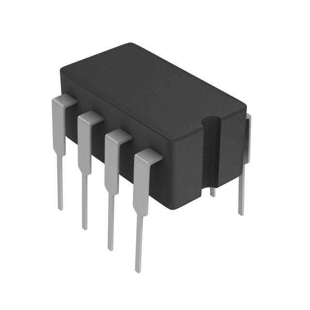
| 描述 | IC REG BOOST SYNC 5V 1.5A 8DFN |
| 产品分类 | |
| 品牌 | Linear Technology |
| 数据手册 | http://www.linear.com/docs/27557 |
| 产品图片 |
|
| 产品型号 | LTC3529EDCB#TRMPBF |
| PWM类型 | 电流模式 |
| rohs | 无铅 / 符合限制有害物质指令(RoHS)规范要求 |
| 产品系列 | - |
| 产品目录页面 | |
| 供应商器件封装 | 8-DFN(3x2) |
| 其它名称 | LTC3529EDCB#TRMPBFDKR |
| 包装 | Digi-Reel® |
| 同步整流器 | 是 |
| 安装类型 | 表面贴装 |
| 封装/外壳 | 8-WFDFN 裸露焊盘 |
| 工作温度 | -40°C ~ 85°C |
| 标准包装 | 1 |
| 电压-输入 | 1.8 V ~ 5.25 V |
| 电压-输出 | 5V |
| 电流-输出 | 1.5A |
| 类型 | 升压(升压) |
| 输出数 | 1 |
| 输出类型 | 固定 |
| 频率-开关 | 1.5MHz |


- 商务部:美国ITC正式对集成电路等产品启动337调查
- 曝三星4nm工艺存在良率问题 高通将骁龙8 Gen1或转产台积电
- 太阳诱电将投资9.5亿元在常州建新厂生产MLCC 预计2023年完工
- 英特尔发布欧洲新工厂建设计划 深化IDM 2.0 战略
- 台积电先进制程称霸业界 有大客户加持明年业绩稳了
- 达到5530亿美元!SIA预计今年全球半导体销售额将创下新高
- 英特尔拟将自动驾驶子公司Mobileye上市 估值或超500亿美元
- 三星加码芯片和SET,合并消费电子和移动部门,撤换高东真等 CEO
- 三星电子宣布重大人事变动 还合并消费电子和移动部门
- 海关总署:前11个月进口集成电路产品价值2.52万亿元 增长14.8%


PDF Datasheet 数据手册内容提取
LTC3529 1.5A, 1.5MHz Step-Up DC/DC Converter in × 2mm 3mm DFN FEATURES DESCRIPTION n Compact Solution for 5V USB On-The-Go The LTC®3529 is a 5V output, synchronous, fi xed frequency V Power step-up DC/DC converter optimized for USB On-The-Go BUS n 5V at 500mA from Single Li-Ion Cell (OTG) hosting applications. This compact USB OTG 5V n Automatic Fault Detection V converter features a 1.5MHz switching frequency, BUS n High Effi ciency: Up to 95% internal compensation and a tiny 2mm × 3mm DFN pack- n V Range: 1.8V to 5.25V age. The LTC3529 can operate from input voltages as low IN n Fixed 5V Output as 1.8V. n Short-Circuit Protection USB OTG-specifi c features include a fault fl ag with 22ms n 1.5MHz Low Noise, Fixed Frequency PWM deglitching to indicate when the bus is overloaded, output n Inrush Current Limiting and Internal Soft-Start disconnect and short-circuit protection. Following a fault, n Output Disconnect the LTC3529 can be programmed to either latchoff or n <1μA Quiescent Current in Shutdown restart after a time-out duration. n V > V Operation IN OUT n 8-Lead, 2mm × 3mm DFN Package Additional features include a <1μA shutdown mode, soft-start, inrush current limiting and thermal overload APPLICATIONS protection. Anti-ring circuitry reduces EMI during low power operation. The LTC3529 is offered in an 8-lead n Personal Media Players 2mm × 3mm × 0.75mm DFN package. n Digital Video Cameras L, LT, LTC, LTM, Linear Technology and the Linear logo are registered trademarks of Linear n Digital Multimedia Broadcast Tuners Technology Corporation. All other trademarks are the property of their respective owners. Protected by U.S. Patents including 6404251, 6166527. n Digital Cameras n Smart Phones TYPICAL APPLICATION Li-Ion Battery to 5V Synchronous Boost Converter Effi ciency vs Load Current 100 0.9 4.7μH 90 0.8 2.5V+ TO Li-Ion 3.3μF LTC3529 80 EFFICIENCY 0.7 4.2V 370Ω VFAINULT SNSGSNWD ENCY (%) 765000 00..65 POWER LO AUTO-RESTART OFF ON RST VOUT COUT V55V0O0UmTA EFFICI 3400 00..43 SS (W) 10μF 20 0.2 OFF ON SHDN PGND 10 POWER LOSS 0.1 3529 TA01a 0 0 1 10 100 1000 LOAD CURRENT (mA) VIN = 3.6V 3529 TA01b INDUCTOR = 4.7μH, COOPER BUSSMANN SD25-4R7 3529fb 1
LTC3529 ABSOLUTE MAXIMUM RATINGS PIN CONFIGURATION (Note 1) TOP VIEW V , V Voltage ...........................................–0.3 to 6V IN OUT SHDN, RST, FAULT Voltage ............................–0.3 to 6V VOUT 1 8 VIN SW Voltage SW 2 7 RST 9 DC ..............................................................–0.3 to 6V SHDN 3 6 SNSGND PGND 4 5 FAULT Pulsed <100ns .............................................–1V to 7V Operating Temperature Range (Note 2) ...–40°C to 85°C DCB PACKAGE 8-LEAD (2mm (cid:115) 3mm) PLASTIC DFN Maximum Junction Temperature (Note 3) ............125°C TJMAX = 125°C, θJA = 64°C/W Storage Temperature Range ..................–65°C to 125°C EXPOSED PAD (PIN 9) IS GND, MUST BE SOLDERED TO PCB ORDER INFORMATION LEAD FREE FINISH TAPE AND REEL PART MARKING PACKAGE DESCRIPTION TEMPERATURE RANGE LTC3529EDCB#PBF LTC3529EDCB#TRPBF LCTZ 8-Lead (2mm × 3mm) Plastic DFN –40°C to 85°C Consult LTC Marketing for parts specifi ed with wider operating temperature ranges. Consult LTC Marketing for information on non-standard lead based fi nish parts. For more information on lead free part marking, go to: http://www.linear.com/leadfree/ For more information on tape and reel specifi cations, go to: http://www.linear.com/tapeandreel/ ELECTRICAL CHARACTERISTICS The l denotes the specifi cations which apply over the full operating temperature range, otherwise specifi cations are at T = 25°C. V = 3.6V, V = 5V unless otherwise noted. A IN OUT PARAMETER CONDITIONS MIN TYP MAX UNITS Input Voltage Range 1.8 5.25 V Output Voltage l 4.85 5 5.15 V Quiescent Current - Shutdown V = 0V, V = 0V 0.01 1 μA SHDN OUT NMOS Switch Leakage Current V = V = 5V l 0.3 15 μA IN SW PMOS Switch Leakage Current V = 0V, V = 5V l 0.3 15 μA SW OUT NMOS Switch On Resistance 0.09 Ω PMOS Switch On Resistance 0.12 Ω NMOS Current Limit V = 4.5V (Note 4) l 1.5 A OUT Current Limit Delay Time to Output (Note 5) 40 ns Maximum Duty Cycle V = 4.5V l 80 87 % OUT Minimum Duty Cycle V = 5.5V l 0 % OUT Switching Frequency V = 4.5V l 1.2 1.5 1.8 MHz OUT SHDN, RST Input High Voltage l 1 V SHDN, RST Input Low Voltage l 0.35 V SHDN, RST Input Current V , V , V = 5.5V l 0.01 1 μA SHDN OUT RST Soft-Start Time 2 ms Line Regulation V = 1.8V to 5.25V 0.03 %/V IN 3529fb 2
LTC3529 ELECTRICAL CHARACTERISTICS The l denotes the specifi cations which apply over the full operating temperature range, otherwise specifi cations are at T = 25°C. V = 3.6V, V = 5V unless otherwise noted. A IN OUT PARAMETER CONDITIONS MIN TYP MAX UNITS FAULT Delay Time V = 0V 12 22 35 ms OUT FAULT Output Low Voltage I = 5mA, V = 0V 60 mV FAULT OUT FAULT Leakage Current V = 5.5V 10 μA FAULT Note 1: Stresses beyond those listed under Absolute Maximum Ratings Note 3: This IC includes overtemperature protection that is intended may cause permanent damage to the device. Exposure to any Absolute to protect the device during momentary overload conditions. Junction Maximum Rating condition for extended periods may affect device temperature will exceed 125°C when overtemperature protection is active. reliability and lifetime. Continuous operation above the specifi ed maximum operating junction Note 2: The LTC3529 is guaranteed to meet performance specifi cations temperature may impair device reliability. from 0°C to 85°C. Specifi cations over the –40°C to 85°C operating Note 4: Current measurements are performed when the LTC3529 is not temperature range are assured by design, characterization and correlation switching. The current limit values in operation will be somewhat higher with statistical process controls. due to the propagation delay of the comparators. Note 5: Specifi cation is guaranteed by design and not 100% tested in production. TYPICAL PERFORMANCE CHARACTERISTICS 2 Alkaline Cells to 5V Effi ciency Li-Ion Battery to 5V Effi ciency 100 100 0.7 VIN = 3V 0.7 VIN = 4.1V 90 90 VIN = 3.6V 80 EFFICIENCY VIN = 1.8V 0.6 80 VIN = 3V 0.6 EFFICIENCY (%)76540000 000...543POWER LOSS (W EFFICIENCY (%)76540000 EFFICIENCY 000...543POWER LOSS (W 30 VIN = 1.8V 0.2) 30 0.2) 20 20 POWER LOSS 0.1 POWER LOSS 0.1 10 10 VIN = 3V 0 0 0 0 1 10 100 1000 1 10 100 1000 LOAD CURRENT (mA) LOAD CURRENT (mA) COUT = 10μF 3529 G01 COUT = 10μF 3529 G02 INDUCTOR = 4.7μH, INDUCTOR = 4.7μH, COOPER BUSSMANN SD25-4R7 COOPER BUSSMANN SD25-4R7 Soft-Start Waveforms Load Transient Response V Ripple OUT VOUT 5V/DIV VOUT IL 200mV/DIV 200mA/DIV SHDN 500mA/DIIVL 5mVV/ODUIVT 5V/DIV 2ms/DIV 3529 G03 200μs/DIV 3529 G04 1μs/DIV 3529 G05 VIN = 3.6V VIN = 3.6V VIN = 3.6V VOUT = 5V VOUT = 5V COUT = 10μF COUT = 10μF COUT = 10μF L = 4.7μH L = 2.2μH L = 2.2μH ILOAD = 200mA 3529fb 3
LTC3529 TYPICAL PERFORMANCE CHARACTERISTICS Output Voltage Change Current Limit vs Temperature vs Temperature Maximum Output Current vs V IN 1.90 1.0 1600 L = 4.7μH 1.85 0.8 1400 1.80 0.6 %) 1200 RRENT LIMIT (A)1111....66775050 GE FROM 25°C (–000...4220 I (mA)OUT1086000000 U N C1.55 HA–0.4 C 400 1.50 –0.6 200 1.45 –0.8 1.40 –1.0 0 –45 –25 –5 15 35 55 75 95 115 –50 0 50 100 150 1.5 2.0 2.5 3.0 3.5 4.0 4.5 5.0 TEMPERATURE (°C) TEMPERATURE (°C) VIN (V) 3529 G06 3529 G07 3529 G08 Switching Frequency Variation SW Pin Anti-Ringing vs Temperature No-Load Input Current vs V IN 10 18 IL 8 16 25mA/DIV %) 6 mA)14 5°C ( 4 NT (12 2V/DSIWV D TO 2 02 CURRE10 1μs/DIV 3529 G09 RMALIZE––42 ESCENT 86 VCIONU =T =3 .160VμF NO–6 QUI 4 L = 4.7μH –8 2 –10 0 –50 –30 –10 10 30 50 70 90 110 1.5 2.5 3.5 4.5 5.5 TEMPERATURE (°C) VIN (V) 3529 G10 3529 G11 R vs Temperature Load Regulation DS(ON) 160 0.5 VIN = 3.3V 140 PMOS 0.4 L = 4.7μH 0.3 120 %) 0.2 R (mΩ)DS(ON)1086000 NMOS CHANGE (OUT–00..110 V –0.2 40 –0.3 20 –0.4 0 –0.5 –50 –25 0 25 50 75 100 125 0 100 200 300 400 500 TEMPERATURE (°C) ILOAD (mA) 3529 G12 3529 G13 3529fb 4
LTC3529 PIN FUNCTIONS V (Pin 1): Converter Output, Voltage Sense Input SNSGND (Pin 6): This pin must be connected to OUT and Drain of the Internal Synchronous Rectifi er MOSFET. ground. Driver bias is derived from V . PCB trace length from OUT RST (Pin 7): Logic Input to Select Automatic Restart or V to the output fi lter capacitor(s) should be as short OUT Latchoff Following a Fault Shutdown. and wide as possible. • RST = High: Auto-reset mode. In this mode, the LTC3529 SW (Pin 2): Switch Node. This node connects to one will automatically attempt to restart 22ms (typically) side of the inductor. Keep PCB traces as short and wide after a fault shutdown. as possible to reduce EMI and voltage overshoot. If the inductor current falls to zero, or SHDN is low, an internal • RST = Low: Latchoff mode. In this mode, the LTC3529 100Ω anti-ringing switch is connected between SW and will latch off for a fault shutdown. The IC will not restart V to minimize EMI. until the SHDN pin is toggled or the supply voltage is IN cycled. SHDN (Pin 3): Active-Low Shutdown Input. Forcing this pin above 1V enables the converter. Forcing this pin below VIN (Pin 8): Input Supply Pin. 0.35V disables the converter. Do not fl oat this pin. Exposed Pad (Pin 9): Small Signal Ground. This is the PGND (Pin 4): High Current Ground Connection. The PCB ground reference for the internal circuitry of the LTC3529 trace connecting this pin to ground should be as short and and must be connected directly to ground. as wide as possible. FAULT (Pin 5): Open-Drain Fault Indicator Output. Pulls low when an overcurrent condition exists for more than 22ms. 3529fb 5
LTC3529 BLOCK DIAGRAM L1 4.7μH VIN 1.T8OV+– C3.I3NμF 8 VIN 3 SHDN 2 SW BULK CONTROL 5.25V SIGNALS VIN ANTI-RING 1 VOUT, 5V VOUT COUT 10μF 6 SNSGND CLOCK PWM LOGIC AND DRIVERS + – IZERO COMP CURRENT SENSE 5 FAULT OR THERMAL FAULT SHUTDOWN REFERENCE 1.25V 22ms THERMAL SD FAULT TIMER PWM SOFT-START R1 COMP 1.875M ILIM + – SD – COMP GM ERROR – + AMPLIFIER + + 1.25V (cid:51) RC + R2 C2 625k OSCILLATOR 2A CC RST PGND GND (BP) 7 4 9 3529 BD OPERATION The LTC3529 is a 1.5MHz synchronous boost converter in light loads, the LTC3529 will exhibit pulse-skipping an 8-lead 2mm × 3mm DFN package. The device operates operation. with an input voltage as low as 1.8V and features fi xed- frequency current-mode PWM control for exceptional line Soft-Start and load regulation. Internal MOSFET switches with low The LTC3529 provides soft-start by ramping the inductor R and low gate charge enable the device to maintain DS(ON) current limit from zero to its peak value in approximately high effi ciency over a wide range of load current. 2ms. The internal soft-start capacitor is discharged in the event of a fault, thermal shutdown or when the IC is PWM Operation disabled via the SHDN pin. The LTC3529 operates in a fi xed-frequency PWM mode using current-mode control at all load currents. At very 3529fb 6
LTC3529 OPERATION Oscillator latchoff mode is highly recommended for maximum level of robustness. An internal oscillator sets the switching frequency to 1.5MHz. Note: When VOUT is released from a short-circuit condi- tion, it is possible for the output to momentarily exceed Shutdown the maximum output voltage rating. In cases where repeated shorts are expected, V should be protected The LTC3529 is shut down by pulling the SHDN pin below OUT by the addition of a 5.6V Zener clamp from V to GND. 0.35V, and activated by pulling the SHDN pin above 1V. Note OUT Alternatively, C can be increased to 47μF or greater. that SHDN can be driven above V or V , as long as it OUT IN OUT is limited to less than the absolute maximum rating. Zero-Current Comparator Error Amplifi er The zero-current comparator monitors the inductor cur- rent to the output and shuts off the synchronous rectifi er The error amplifi er is a transconductance amplifi er with when this current falls below approximately 20mA. This an internal compensation network. Internal clamps limit prevents the inductor current from reversing in polarity, the minimum and maximum error amplifi er output voltage thereby improving effi ciency at light loads. to improve the large-signal transient response. Anti-Ringing Control Current Sensing The anti-ringing circuit connects a resistor across the Lossless current sensing converts the peak current sig- inductor to damp the ringing on SW in discontinuous nal of the N-channel MOSFET switch into a voltage that conduction mode. The ringing of the resonant circuit is summed with the internal slope compensation. The formed by L and C (capacitance on the SW pin) is low SW summed signal is compared to the error amplifi er output energy but can cause EMI radiation. to provide a peak current control command for the PWM. Peak switch current is limited to approximately 2A inde- Output Disconnect pendent of input or output voltage. The LTC3529 provides true output disconnect by eliminating body diode conduction of the internal P-channel MOSFET Current Limit rectifi er. This allows V to go to zero volts during shut- OUT The current limit comparator shuts off the N-channel MOSFET down, drawing no current from the input source. It also switch when the current limit threshold is reached. The current provides inrush current limiting at turn-on, minimizing limit comparator delay time to output is typically 40ns. surge currents seen by the input supply. Fault Detection Thermal Shutdown To prevent the device from providing power to a shorted If the die temperature reaches approximately 160°C, output, the switch current is monitored to detect an the device enters thermal shutdown, the fault fl ag is overcurrent condition. In the event that the switch current asserted (FAULT pulls low) and all switches are turned off. reaches the current limit for longer than 22ms, the fault The device is enabled and a soft-start sequence is initiated fl ag is asserted (FAULT pulls low) and the device is shut when the die temperature drops by approximately 10°C. down. If the auto-restart option is enabled (RST high), the PCB Layout device will automatically attempt to restart every 22ms until the short is removed. If auto-restart is disabled (RST Due to the high frequency operation of the LTC3529, board low), the IC will remain shut down until being manually layout is extremely critical to minimize transients caused by restarted by toggling SHDN or cycling the input voltage. stray inductance. Keep the output fi lter capacitor as close A soft-start sequence is initiated when the device restarts. as possible to the V pin and use very low ESR/ESL OUT If output short-circuits are common in the application, ceramic capacitors tied to a good ground plane. 3529fb 7
LTC3529 APPLICATIONS INFORMATION The basic LTC3529 application circuit is shown in the Typi- Although ceramic capacitors are recommended, low ESR cal Application on the front page. The external component tantalum capacitors may also be used. A small ceramic selection is determined by the desired output current and capacitor in parallel with a larger tantalum capacitor is ripple voltage requirements of each particular application. recommended in demanding applications that have large However, basic guidelines and considerations for the design load transients. process are provided in this section. Input Capacitor Selection Output Capacitor Selection Low ESR input capacitors reduce input switching noise A low ESR (equivalent series resistance) output capacitor and reduce the peak current drawn from the battery. It should be used at the output of the LTC3529 to minimize follows that ceramic capacitors are also a good choice the output voltage ripple. Multilayer ceramic capacitors are for input decoupling and should be located as close as an excellent choice as they have extremely low ESR and possible to the device. A 3.3μF input capacitor is suffi cient are available in small footprints. X5R and X7R dielectric for most applications. Larger values may be used without materials are strongly recommended over Y5V dielectric limitation. because of their improved voltage and temperature coef- fi cients. Neglecting the capacitor ESR and ESL (equivalent Capacitor Vendor Information series inductance), the peak-to-peak output voltage ripple Both the input and output capacitors used with the LTC3529 can be calculated by the following formula, where f is the must have low ESR and be designed to handle the large frequency in MHz, C is the capacitance in μF, and I OUT LOAD AC currents generated by switching converters. The ven- is the output current in amps. dors in Table 1 provide capacitors that are well suited to ( ) LTC3529 application circuits. I V –V ΔV = LOAD OUT IN P−P C (cid:129)V (cid:129)f Table 1. Capacitor Vendor Information OUT OUT MANUFACTURER WEB SITE PHONE FAX The internal loop compensation of the LTC3529 is designed Taiyo Yuden www.t-yuden.com (408) 573-4150 (408) 573-4159 to be stable with output capacitor values of 6.5μF or greater. TDK www.component. (847) 803-6100 (847) 803-6296 This complies with USB On-The-Go specifi cations, which tdk.com limit the output capacitance to 6.5μF. In general use of the Sanyo www.secc.co.jp (619) 661-6322 (619) 661-1055 LTC3529, the output capacitor should be chosen large AVX www.avxcorp.com (803) 448-9411 (803) 448-1943 enough to reduce the output voltage ripple to acceptable Murata www.murata.com (814) 237-1431 (814) 238-0490 levels. A 6.8μF to 10μF output capacitor is suffi cient for Sumida www.sales@ (408) 321-9660 (408) 321-9308 most applications. Larger values up to 22μF may be used us.sumida.com to obtain extremely low output voltage ripple and improved transient response. 3529fb 8
LTC3529 APPLICATIONS INFORMATION Inductor Selection PCB Layout Guidelines The LTC3529 can utilize small surface-mount chip induc- The LTC3529 switches large currents at high frequencies. tors due to its fast 1.5MHz switching frequency. Larger Special care should be given to the PCB layout to ensure values of inductance will allow slightly greater output stable, noise-free operation. Figure 1 depicts the recom- current capability by reducing the inductor ripple current. mended PCB layout to be utilized for the LTC3529. A few Increasing the inductance above 10μH will increase com- key guidelines follow: ponent size while providing little improvement in output 1. All circulating current paths should be kept as short current capability. as possible. This can be accomplished by keeping the USB On-The-Go specifi cations limit output capacitance to copper traces to all components in Figure 1 short and 6.5μF. When using a 6.5μF output capacitance, a 4.7μH wide. Capacitor ground connections should via down inductor must be used to maintain stability. Larger induc- to the ground plane in the shortest route possible. The tors may be used with larger output capacitors. bypass capacitors on V and V should be placed IN OUT The minimum inductance value for a given allowable induc- close to the IC and should have the shortest possible tor ripple ΔI (in Amps peak-to-peak) is given by: paths to ground. ( ) 2. The PGND pin should be shorted directly to the ex- V (cid:129) V –V IN(MIN) OUT IN(MIN) L> µH posed pad, as shown in Figure 1. This provides a single ΔI(cid:129)f(cid:129)V OUT point connection between the small signal ground and the power ground, as well as a wide trace for power where V is the minimum input voltage, f is the IN(MIN) ground. operating frequency in MHz (1.5MHz Typ), and V is OUT the output voltage (5V). 3. All the external components shown in Figure 1 and their connections should be placed over a complete ground The inductor current ripple is typically set for 20% to 40% plane. of the maximum inductor current (I ). High frequency P ferrite core inductor materials reduce frequency depen- 4. Use of multiple vias in the die attach pad will enhance dent power losses compared to cheaper powdered iron the thermal environment of the converter, especially if cores, improving effi ciency. To achieve high effi ciency, a the vias extend to a ground plane region on the exposed low ESR inductor should be utilized. The inductor must bottom surface or inner layers of the PCB. have a saturation current rating greater than the worst case average inductor current plus half the ripple current. Molded chokes and some chip inductors usually do not have enough core to support peak LTC3529 inductor currents. To minimize radiated noise, use a shielded inductor. See Table 2 for suggested components and suppliers. VOUT 1 8 VIN SW 2 7 RST Table 2. Representative Surface Mount Inductors SHDN 3 6 SNSGND MAX PGND 4 5 FAULT MANUFACTURER PART NUMBER VALUE CURRENT DCR HEIGHT (μH) (A) (Ω) (mm) MULTIPLE VIAs TO GROUND PLANE Sumida CDRH5D16NP 4.7 2.15 0.064 1.8 Figure 1. LTC3529 Recommended PCB Layout TDK VLF5014S 4.7 2 0.098 1.4 Coilcraft MSS6122 4.7 1.82 0.065 2.2 Cooper Bussmann SD25-4R7 4.7 2.3 0.043 2.5 3529fb 9
LTC3529 TYPICAL APPLICATIONS Li-Ion Battery to 5V at 100mA or 500mA for USB OTG Host Supply L1* 4.7μH 2.5V+ TO Li-Ion 3.3μF LTC3529 4.2V 1.8V VIN SW 1M TO μP FAULT SNSGND AUTO-RESTART OFF ON RST VOUT VOUT, 5V COUT 6.8μF OFF ON SHDN PGND *L1: SUMIDA CDRH5D16NP 3529 TA02a Overcurrent Event Overcurrent Event V High V Low RST RST VOUT VOUT 5V/DIV 5V/DIV LOAD LOAD CURRENT CURRENT 1A/DIV 1A/DIV FAULT FAULT 2V/DIV 2V/DIV 20ms/DIV 3529 TA02b 20ms/DIV 3529 TA02c 2 Alkaline Cells to 5V at 350mA 2 Alkaline Cells to 5V Effi ciency L1* 100 4.7μH 90 VIN = 3V 0.7 1.8V+ 80 EFFICIENCY VIN = 1.8V 0.6 3.T2OV 2A-LCKEALLLINE C3.I3NμF 270Ω VFAINULTLTC3S5N2S9GSNWD ENCY (%)765000 00..54POWER LO AUTO-RESTART OFF ON RST VOUT VOUT, 5V EFFICI3400 VIN = 1.8V 0.3SS (W) COUT 0.2 6.8μF 20 OFF ON SHDN PGND 10 POWER LOSS 0.1 VIN = 3V 0 0 *L1: SUMIDA CDRH5D16NP 3529 TA03a 1 10 100 1000 LOAD CURRENT (mA) COUT = 6.8μF 3529 TA03b INDUCTOR = 4.7μH, COOPER BUSSMANN SD25-4R7 3529fb 10
LTC3529 PACKAGE DESCRIPTION DCB Package 8-Lead Plastic DFN (2mm × 3mm) (Reference LTC DWG # 05-08-1718 Rev A) 0.70 ±0.05 3.50 ±0.05 1.35 ±0.05 1.65 ± 0.05 2.10 ±0.05 PACKAGE OUTLINE 0.25 ± 0.05 0.45 BSC 1.35 REF RECOMMENDED SOLDER PAD PITCH AND DIMENSIONS APPLY SOLDER MASK TO AREAS THAT ARE NOT SOLDERED 2.00 ±0.10 R = 0.115 0.40 ± 0.10 (2 SIDES) TYP R = 0.05 5 8 TYP 1.35 ±0.10 3.00 ±0.10 1.65 ± 0.10 (2 SIDES) PIN 1 NOTCH PIN 1 BAR R = 0.20 OR 0.25 TOP MARK × 45° CHAMFER (SEE NOTE 6) (DCB8) DFN 0106 REV A 4 1 0.23 ± 0.05 0.200 REF 0.75 ±0.05 0.45 BSC 1.35 REF BOTTOM VIEW—EXPOSED PAD 0.00 – 0.05 NOTE: 1. DRAWING IS NOT A JEDEC PACKAGE OUTLINE 2. DRAWING NOT TO SCALE 3. ALL DIMENSIONS ARE IN MILLIMETERS 4. DIMENSIONS OF EXPOSED PAD ON BOTTOM OF PACKAGE DO NOT INCLUDE MOLD FLASH. MOLD FLASH, IF PRESENT, SHALL NOT EXCEED 0.15mm ON ANY SIDE 5. EXPOSED PAD SHALL BE SOLDER PLATED 6. SHADED AREA IS ONLY A REFERENCE FOR PIN 1 LOCATION ON THE TOP AND BOTTOM OF PACKAGE 3529fb Information furnished by Linear Technology Corporation is believed to be accurate and reliable. 11 However, no responsibility is assumed for its use. Linear Technology Corporation makes no representa- tion that the interconnection of its circuits as described herein will not infringe on existing patent rights.
LTC3529 RELATED PARTS PART NUMBER DESCRIPTION COMMENTS LTC3400/LTC3400B 600mA (I ), 1.2MHz, Synchronous Step-Up DC/DC 92% Effi ciency, V : 0.85V to 5V, V = 5V, I = 19μA/300μA, SW IN OUT(MAX) Q Converter I <1μA, ThinSOT™ Package SD LTC3401 1A (I ), 3MHz, Synchronous Step-Up DC/DC Converter 97% Effi ciency, V : 0.85V to 5V, V = 5.5V, I = 38μA, I <1μA, SW IN OUT(MAX) Q SD MS10 Package LTC3402 2A (I ), 3MHz, Synchronous Step-Up DC/DC Converter 97% Effi ciency, V : 0.85V to 5V, V = 5.5V, I = 38μA, I <1μA, SW IN OUT(MAX) Q SD MS10 Package LTC3421 3A (I ), 3MHz Synchronous Step-Up DC/DC Converter 94% Effi ciency, V : 0.85V to 4.5V, V = 5.25V, I = 12μA, SW IN OUT(MAX) Q with Output Disconnect I <1μA, 4mm × 4mm QFN-24 Package SD LTC3422 1.5A (I ), 3MHz Synchronous Step-Up DC/DC with 94% Effi ciency, V : 0.85V to 4.5V, V = 5.25V, I = 25μA, SW IN OUT(MAX) Q Output Disconnect Converter I <1μA, 3mm × 3mm DFN-10 Package SD LTC3426 2A (I ), 1.5MHz, Step-Up DC/DC Converter 92% Effi ciency, V : 1.6V to 5.5V, V = 5V, I = 600μA, I <1μA, SW IN OUT(MAX) Q SD ThinSOT Package LTC3427 500mA (I ), 1.25MHz Synchronous Step-Up DC/DC 94% Effi ciency, V : 1.8V to 5V, V = 5.25V, I = 350μA, SW IN OUT(MAX) Q Converter with Output Disconnect I <1μA, 2mm × 2mm DFN-6 Package SD LTC3429/LTC3429B 600mA (I ), 550kHz, Synchronous Step-Up DC/DC 96% Effi ciency, V : 0.85V to 4.3V, V = 5V, I = 20μA, I <1μA, SW IN OUT(MAX) Q SD Converter with Soft-Start/Output Disconnect ThinSOT Package LTC3458/LTC3458L 1.4A/1.7A (I ), 1.5MHz Synchronous Step-Up DC/DC 94% Effi ciency, V : 0.85V to 6V, V = 7.5V/6V, I = 15μA, SW IN OUT(MAX) Q I <1μA, 3mm × 4mm DFN-12 Package SD LTC3459 80mA (I ), Synchronous Step-Up DC/DC Converter 92% Effi ciency, V : 1.5V to 5.5V, V = 10V, I = 10μA, I <1μA, SW IN OUT(MAX) Q SD ThinSOT Package LT3494/LT3494A 180mA/350mA (I ), High Effi ciency Step-Up DC/DC 85% Effi ciency, V : 2.3V to 16V, V = 38V, I = 65μA, I <1μA, SW IN OUT(MAX) Q SD Converter with Output Disconnect 2mm × 3mm DFN-6, ThinSOT Package LTC3525-3/ 400mA (I ), Synchronous Step-Up DC/DC Converter 94% Effi ciency, V : 0.85V to 4V, V = 3V/3.3V/5V, I = 7μA, SW IN OUT(MAX) Q LTC3525-3.3/ with Output Disconnect I <1μA, SC-70 Package SD LTC3525-5 LTC3526/LTC3526L/ 500mA (I ), 1MHz Synchronous Step-Up DC/DC 94% Effi ciency, V : 0.85V to 5V, V = 5.25V, I = 9μA, I <1μA, SW IN OUT(MAX) Q SD LTC3526B Converter with Output Disconnect 2mm × 2mm DFN-6 Package LTC3527/LTC3527-1 Dual 800mA and 400mA (I ), 2.2MHz, Synchronous 94% Effi ciency, V : 0.7V to 5V, V = 5.25V, I = 12μA, I <1μA, SW IN OUT(MAX) Q SD Step-Up DC/DC Converter with Output Disconnect 3mm × 3mm QFN-16 Package LTC3528 1A (I ), 1MHz Synchronous Step-Up DC/DC Converter 94% Effi ciency, V : 0.7V to 5V, V = 5.25V, I = 12μA, I <1μA, SW IN OUT(MAX) Q SD with Output Disconnect 2mm × 3mm DFN-8 Package LTC3537 600mA, 2.2MHz, Synchronous Step-Up DC/DC Converter 94% Effi ciency, V : 0.7V to 5V, V = 5.25V, I = 30μA, I <1μA, IN OUT(MAX) Q SD with Output Disconnect and 100mA LDO 3mm × 3mm QFN-16 Package LTC3539 2A , 2MHz, Synchronous Step-Up DC/DC Converter with 94% Effi ciency, V : 0.7V to 5V, V = 5.25V, I = 10μA, I <1μA, IN OUT(MAX) Q SD Output Disconnect 2mm × 3mm DFN-8 Package ThinSOT is a trademark of Linear Technology Corporation. 3529fb 12 Linear Technology Corporation LT 0709 REV B • PRINTED IN USA 1630 McCarthy Blvd., Milpitas, CA 95035-7417 (408) 432-1900 ● FAX: (408) 434-0507 ● www.linear.com © LINEAR TECHNOLOGY CORPORATION 2009