ICGOO在线商城 > 集成电路(IC) > PMIC - 稳压器 - 线性 + 切换式 > LTC3446IDE#PBF
/LTC3446IDE#PBF.jpg)
 Datasheet下载
- 型号: LTC3446IDE#PBF
- 制造商: LINEAR TECHNOLOGY
- 库位|库存: xxxx|xxxx
- 要求:
| 数量阶梯 | 香港交货 | 国内含税 |
| +xxxx | $xxxx | ¥xxxx |
查看当月历史价格
查看今年历史价格
LTC3446IDE#PBF产品简介:
ICGOO电子元器件商城为您提供LTC3446IDE#PBF由LINEAR TECHNOLOGY设计生产,在icgoo商城现货销售,并且可以通过原厂、代理商等渠道进行代购。 LTC3446IDE#PBF价格参考。LINEAR TECHNOLOGYLTC3446IDE#PBF封装/规格:PMIC - 稳压器 - 线性 + 切换式, Linear And Switching Voltage Regulator IC 3 Output Step-Down (Buck) Synchronous (1), Linear (LDO) (2) 2.25MHz 14-DFN (4x3)。您可以下载LTC3446IDE#PBF参考资料、Datasheet数据手册功能说明书,资料中有LTC3446IDE#PBF 详细功能的应用电路图电压和使用方法及教程。
| 参数 | 数值 |
| 产品目录 | 集成电路 (IC) |
| 描述 | IC REG TRPL BCK/LINEAR 14-DFN |
| 产品分类 | |
| 品牌 | Linear Technology |
| 数据手册 | http://www.linear.com/docs/16418 |
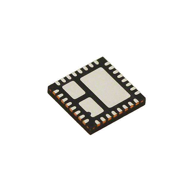
| 产品图片 |
|
| 产品型号 | LTC3446IDE#PBF |
| rohs | 无铅 / 符合限制有害物质指令(RoHS)规范要求 |
| 产品系列 | - |
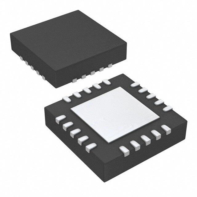
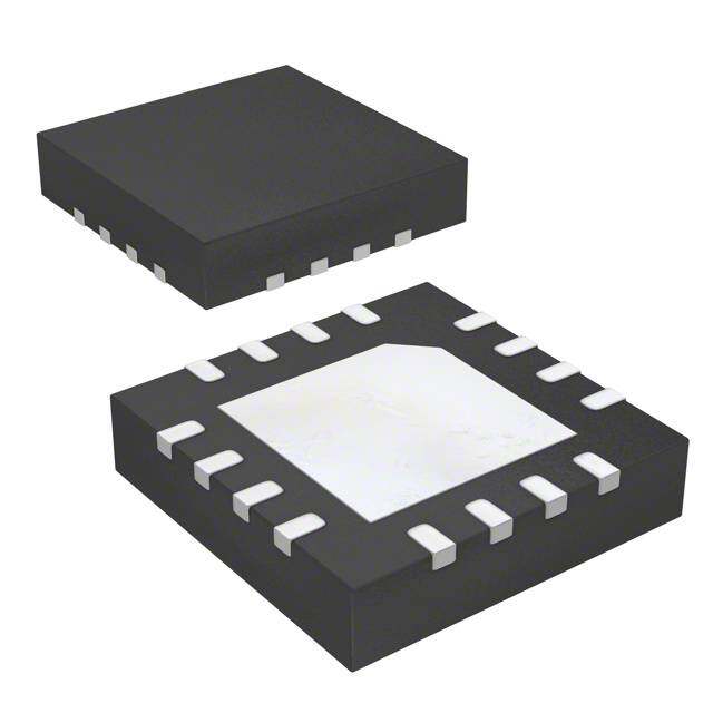
| 供应商器件封装 | 14-DFN(4x3) |
| 其它名称 | LTC3446IDEPBF |
| 功能 | 任何功能 |
| 包装 | 管件 |
| 安装类型 | 表面贴装 |
| 封装/外壳 | 14-WFDFN 裸露焊盘 |
| 工作温度 | -40°C ~ 125°C |
| 带LED驱动器 | 无 |
| 带定序器 | 无 |
| 带监控器 | 无 |
| 拓扑 | 降压(降压)同步(1),线性(LDO)(2) |
| 标准包装 | 91 |
| 电压-电源 | 0.9 V ~ 5.5 V |
| 电压/电流-输出1 | 可调至0.8V,1A |
| 电压/电流-输出2 | 可调至0.4V,300mA |
| 电压/电流-输出3 | 可调至0.4V,300mA |
| 输出数 | 3 |
| 频率-开关 | 2.25MHz |


- 商务部:美国ITC正式对集成电路等产品启动337调查
- 曝三星4nm工艺存在良率问题 高通将骁龙8 Gen1或转产台积电
- 太阳诱电将投资9.5亿元在常州建新厂生产MLCC 预计2023年完工
- 英特尔发布欧洲新工厂建设计划 深化IDM 2.0 战略
- 台积电先进制程称霸业界 有大客户加持明年业绩稳了
- 达到5530亿美元!SIA预计今年全球半导体销售额将创下新高
- 英特尔拟将自动驾驶子公司Mobileye上市 估值或超500亿美元
- 三星加码芯片和SET,合并消费电子和移动部门,撤换高东真等 CEO
- 三星电子宣布重大人事变动 还合并消费电子和移动部门
- 海关总署:前11个月进口集成电路产品价值2.52万亿元 增长14.8%


PDF Datasheet 数据手册内容提取
LTC3446 Monolithic Buck Regulator with Dual VLDO Regulators FeaTures DescripTion n High Efficiency Triple Step-Down Outputs from a The LTC®3446 combines a synchronous buck DC/DC con- Single Input Supply verter with two very low dropout (VLDO) linear regulators n 1A Synchronous Buck Regulator Provides Main to provide up to three stepped-down output voltages from Step-Down Output and Powers Two 300mA VLDO™ a single input voltage. The input voltage range is ideally Linear Regulators suited for Li-Ion battery-powered applications, as well n Output Voltages as Low as 400mV (VLDO Outputs) as powering low voltage logic from 5V or 3.3V rails. The n Power Good Output output voltage range extends down to 0.4V for the VLDO n Input Voltage Range: 2.7V to 5.5V regulators and 0.8V for the buck. n Independent Enable Pin for Each Supply The 1A synchronous buck converter provides the main n Low (140µA Typ) No-Load Quiescent Current with output with high efficiency, typically 85%. The two 300mA All Outputs Enabled VLDO regulators can run off the main output to provide n Constant Frequency Current Mode Operation two additional lower voltage outputs. A built-in supply n 2.25MHz Switching Frequency Uses Small Inductors monitor provides a power good indication. n Defeatable Automatic Burst Mode® Operation for High Efficiency at Light Loads The buck converter switches at 2.25MHz, allowing the use n ±1.5% Reference Accuracy of small surface mount inductors and capacitors. Constant n Overtemperature Protection frequency current mode operation produces controlled n Thermally Enhanced 4mm × 3mm 14-Pin DFN output spectrum and fast transient response. A mode- Package select pin allows automatic Burst Mode operation to be enabled for higher efficiency at light load, or disabled for applicaTions lower noise operation down to very light loads. The two VLDO regulators are stable with ceramic output capacitors n Low Power Handheld Devices as small as 1µF. n Low Voltage and Multivoltage Power for Digital L, LT, LTC, LTM and Burst Mode are registered trademarks and VLDO, Hot Swap, PowerPath Logic, I/O, FPGAs, CPLDs, ASICs and CPUs and Bat-Track are trademarks of Linear Technology Corporation. All other trademarks are the property of their respective owners. Protected by U.S. Patents including 5481178, 6611131, 6304066, 6498466, 6580258. Typical applicaTion L1 2.9V TO 5V.5IVN 2X27µRF VIN SW 1.8µ5H9k 2X27µRF 14V.0O80UVmTA MAX 1B00uck Efficiency vs Buck Load Current BUCKFB Burst Mode MPWODME 47.5k 90 OPERATION LTC3446 LVIN VOUT %) 80 CODNIGTIRTOALL PMEEENNNGOBLLODDDUOEOOCDS12KELLVLOVUFBT11 4101.02kk 2X.72RµF 13.050VmA MAX EFFICIENCY ( 6700 3.3k VOUT 50 VIN = 2.7V 1000pF ITH LVOUT2 80.6k 2X.72RµF 13.020VmA MAX 40 VVIINN == 34..62VV LVFB2 1 10 100 1000 GND 40.2k LOAD CURRENT (mA) 3446 TA01 L1: TOKO A960AW-1R8M 3446 TA01b 3446ff 1
LTC3446 absoluTe MaxiMuM raTings pin conFiguraTion (Note 1) V , LV to GND ......................................... –0.3V to 6V TOP VIEW IN IN MODESEL, ENBUCK, ENLDO1, MODESEL 1 14 SW ENLDO2 to GND .......................................... –0.3V to 6V VIN 2 13 ENBUCK BUCKFB to GND .......................................... –0.3V to 6V ITH 3 12 BUCKFB PGOOD 4 15 11 ENLDO1 LV , LV to GND .................................... –0.3V to 6V FB1 FB2 LVOUT1 5 10 LVFB1 ITH to GND ..... –0.3V to the Lesser of (VIN + 0.3V) or 3V LVIN 6 9 LVFB2 SW to GND ......–0.3V to the Lesser of (VIN + 0.3V) or 6V LVOUT2 7 8 ENLDO2 LV , LV OUT1 OUT2 DE PACKAGE to GND ..........–0.3V to the Lesser of (LV + 0.3V) or 6V 14-LEAD (4mm × 3mm) PLASTIC DFN IN TJMAX = 125°C, θJA = 43°C/W PGOOD to GND ............................................–0.3V to 6V EXPOSED PAD (PIN 15) IS GND, MUST BE SOLDERED TO PCB LV , LV Short-Circuit OUT1 OUT2 to GND Duration ...............................................Indefinite Operating Junction Temperature Range (Note 2) ..................................................–40°C to 125°C Storage Temperature Range .................. –65°C to 150°C orDer inForMaTion LEAD FREE FINISH TAPE AND REEL PART MARKING* PACKAGE DESCRIPTION TEMPERATURE RANGE LTC3446EDE#PBF LTC3446EDE#TRPBF 3446 14-Lead (4mm × 3mm) Plastic DFN –40°C to 125°C LTC3446IDE#PBF LTC3446IDE#TRPBF 3446 14-Lead (4mm × 3mm) Plastic DFN –40°C to 125°C Consult LTC Marketing for parts specified with wider operating temperature ranges. *The temperature grade is identified by a label on the shipping container. Consult LTC Marketing for information on non-standard lead based finish parts. For more information on lead free part marking, go to: http://www.linear.com/leadfree/ For more information on tape and reel specifications, go to: http://www.linear.com/tapeandreel/ elecTrical characTerisTics The l denotes the specifications which apply over the full operating temperature range, otherwise specifications are at T = 25°C. V = 3.6V unless otherwise specified. (Note 2) A IN SYMBOL PARAMETER CONDITIONS MIN TYP MAX UNITS V Input Voltage Range (Note 3) ● 2.7 5.5 V IN V V Undervoltage Lockout Threshold V Rising ● 2.37 2.5 V UVLO IN IN V Undervoltage Lockout Hysteresis 10 30 mV IN I V Quiescent Current (Note 4) Q IN Buck Enabled Only, Not Sleeping V = 0V, I = 0mA 310 500 µA BUCKFB SW Buck Enabled Only, Sleeping V = 1V, I = 0mA 50 75 µA BUCKFB SW One LDO Enabled Only V = 1.5V, 10µA LDO Output Load 75 100 µA LVIN All Three Outputs Enabled, Buck Not Sleeping V = 0V, I = 0mA, V = 1.5V, 400 600 µA BUCKFB SW LVIN 10µA Output Load on Each LDO All Three Outputs Enabled, Buck Sleeping V = 1V, I = 0mA, V = 1.5V, 140 210 µA BUCKFB SW LVIN 10µA Load on Each LDO Shutdown V = 0V, V = 0V, V = 0V 1 µA ENBUCK ENLDO1 ENLDO2 3446ff 2
LTC3446 elecTrical characTerisTics The l denotes the specifications which apply over the full operating temperature range, otherwise specifications are at T = 25°C. V = 3.6V unless otherwise specified. (Note 2) A IN SYMBOL PARAMETER CONDITIONS MIN TYP MAX UNITS V PGOOD Threshold (Note 8) ● 8 10 % PG(THRESH) R PGOOD Output Resistance PGOOD Low, Sinking 1mA ● 87 180 Ω PGOOD I PGOOD Hi-Z Leakage Current V = 6V ● 1 µA PGOOD PGOOD Synchronous Buck Converter I Feedback Current (Note 5) ● ±30 nA BUCKFB V Regulated Feedback Voltage (Note 5) ● 0.788 0.800 0.812 V BUCKFB ∆VBUCKFB Feedback Voltage Line Regulation VIN = 2.7V to 5.5V (Note 5) ● 0.3 0.5 mV/V I Maximum Peak Inductor Current V = 0V, Duty Cycle < 35% 1.2 1.55 2.0 A MAXP BUCKFB I NMOS Overcurrent Limit 1.8 A MAXN Feedback Voltage Load Regulation V = 0.5V to 1V, V = V (Note 5) 0.5 mV/V ITH MODESEL IN (with Respect to V ) ITH f Oscillator Frequency ● 1.8 2.25 2.7 MHz OSC R R of P-Channel FET I = 500mA 0.13 Ω PFET DS(ON) SW R R of N-Channel FET I = –500mA 0.14 Ω NFET DS(ON) SW I SW Leakage V = 0V, V = 0V or 5.5V, V = 5.5V ±1 µA LSW ENBUCK SW IN V Buck Enable Pin Threshold ● 0.3 0.65 1 V ENBUCK I Buck Enable Pin Leakage Current V = 5.5V, All Other Pins Grounded ● 1 µA ENBUCK ENBUCK V Mode Select Pin Threshold ● 0.3 0.65 1 V MODESEL I Mode Select Pin Leakage Current V = 5.5V, All Other Pins Grounded ● 1 µA MODESEL MODESEL g Error Amplifier Transconductance V = 0.6V 450 700 950 µA/V m ITH Each VLDO: V = 3.6V, V = 1.5V, V = 1.2V, Unless Otherwise Specified IN LVIN LVOUT V LV Pin Operating Voltage (Note 6) ● 0.9 5.5 V LVIN IN I LV Pin Operating Current I = 10µA ● 3 20 µA LVIN IN OUT LV Shutdown Current V = 0V 1.5 2 µA IN ENLDO V Feedback Pin Regulation Voltage (Note 7) 1mA ≤ I ≤ 300mA, 1.5V ≤ V ≤ 5.5V 0.395 0.400 0.405 V LVFB OUT LVIN ● 0.392 0.400 0.408 V I Feedback Pin Input Current V at Regulation ● 2 ±10 nA LVFB LVFB I Continuous Output Current ● 300 mA LVOUT(MAX) Short-Circuit Output Current 760 mA V LDO Enable Pin Threshold ● 0.3 0.65 1 V ENLDOx I LDO Enable Pin Leakage Current V = 5.5V, All Other Pins Grounded ● 1 µA ENLDOx ENLDOx Output Voltage Load Regulation ∆IOUT = 1mA to 300mA –1 mV/A (Referred to the LV Pin) FB L Line Regulation (with Respect to V = 1.5V to 5.5V, V = 3.6V, V = 1.2V, 7.5 µV/V VFB LVIN IN LVOUT the L Pin) I = 1mA VIN OUT L Line Regulation (with Respect to V = 1.5V, V = 2.7V to 5.5V, V = 1.2V, 0.44 mV/V VFB LVIN IN LVOUT the V Pin) I = 1mA IN OUT V LV – LV Dropout Voltage V = 2.8V, V = 1.5V, V = 0.37V, 68 175 mV DO IN OUT IN LVIN LVFB I = 300mA (Note 9) OUT V to LV Headroom Required for I = 300mA l 1.4 V IN OUT LVOUT Regulation (Note 3) 3446ff 3
LTC3446 elecTrical characTerisTics Note 1: Stresses beyond those listed under Absolute Maximum Ratings Note 3: Minimum operating V voltage required for the VLDO regulators IN may cause permanent damage to the device. Exposure to any Absolute to stay in regulation is: Maximum Rating condition for extended periods may affect device V ≥ LV + 1.4V and V ≥ 2.7V IN OUT(MAX) IN reliability and lifetime. Note 4: Dynamic supply current is higher due to the internal gate charge Note 2: The LTC3446 is tested under pulsed load conditions such that being delivered at the switching frequency. T ≈ T . The LTC3446E is guaranteed to meet performance specifications J A Note 5: The LTC3446 is tested in a feedback loop that connects the from 0°C to 85°C operating junction temperature. Specifications over BUCKFB pin to the output of the buck converter’s error amplifier (i.e., the the –40°C to 125°C operating junction temperature range are assured by I pin). TH design characterization and correlation with statistical process controls. Note 6: Minimum operating LV voltage required for the VLDO regulators The LTC3446I is guaranteed to meet performance specifications over IN to stay in regulation is: the –40°C to 125°C operating junction temperature range. Note that the maximum ambient temperature consistent with these specifications is LVIN ≥ LVOUT(MAX) + 100mV and LVIN ≥ 0.9V determined by specific operating conditions in conjunction with board Note 7: Operating conditions are limited by maximum junction layout, the rated package thermal impedance and other environmental temperature. The regulated output voltage specification will not apply factors. The junction temperature (T , in °C) is calculated from the ambient for all possible combinations of input voltage and output current. When J temperature (T , in °C) and power dissipation (P , in Watts) according to operating at maximum input voltage, the output current range must be A D the formula: limited. When operating at maximum output current, the input voltage range must be limited. TJ = TA + (PD • θJA) Note 8: PGOOD assertion indicates that the feedback voltages of all where θJA (in °C/W) is the package thermal impedance. enabled supplies are within the specified percentage of their target values. Note 9: Dropout voltage in the DFN package is assured by design, characterization and statistical process control. Typical perForMance characTerisTics Buck Regulated Feedback Voltage LDO1 Regulated Feedback LDO2 Regulated Feedback vs Temperature Voltage vs Temperature Voltage vs Temperature 808 408 408 806 406 406 804 404 404 V (mV)BUCKFB878090280 V (mV)LVFB1434090280 V (mV)LVFB2434090280 796 VIN = 2.7V 396 VIN = 2.7V 396 VIN = 2.7V VIN = 3.6V VIN = 3.6V VIN = 3.6V 794 VIN = 4.2V 394 VIN = 4.2V 394 VIN = 4.2V VIN = 5.5V VIN = 5.5V VIN = 5.5V 792 392 392 –50 –30 –10 10 30 50 70 90 110 130 –50 –30 –10 10 30 50 70 90 110 130 –50 –30 –10 10 30 50 70 90 110 130 TEMPERATURE (°C) TEMPERATURE (°C) TEMPERATURE (°C) 3446 G01 3446 G02 3446 G03 3446ff 4
LTC3446 Typical perForMance characTerisTics Undervoltage Lockout Threshold Oscillator Frequency vs Temperature Maximum Peak Inductor Current vs Temperature 2.50 2.5 2.50 2.4 2.45 2.45 2.3 2.40 2.2 Hz)2.40 V (V)IN2222....22330550 UVLO FALLING UVLO RISING CURRENT (A) 211112......196870 OR FREQUENCY (M2222....22330550 2.15 1.5 LAT2.15 2.10 11..43 VVIINN == 23..76VV OSCIL2.10 VVIINN == 23..76VV 2.05 1.2 VIN = 4.2V 2.05 VIN = 4.2V 1.1 VIN = 5.5V VIN = 5.5V 2.00 1.0 2.00 –50 –30 –10 10 30 50 70 90 110 130 –50 –30 –10 10 30 50 70 90 110 130 –50 –30 –10 10 30 50 70 90 110 130 TEMPERATURE (°C) TEMPERATURE (°C) TEMPERATURE (°C) 3446 G04 3446 G05 3446 G06 Peak Inductor Current VLDO Current Limit VLDO Dropout Voltage vs I Voltage vs LV Voltage vs Load Current TH IN 1.6 1800 100 VIN = 3.6V VIN = 3.6V VIN = 2.8V 1.4 VMODESEL = 3.6V 1600 LVOUT = 0V 90 LVOUT = 1.2V URRENT (A) 11..20 MIT (mA)11240000 GE (mV) 687000 –29147035°°0CC°°CC NDUCTOR C 00..86 CURRENT LI1806000000 PTJU ≈L STEAD ≈ M 2E7A°CSUREMENT, POUT VOLTA 4500 PEAK I 0.4 VLDO 400 DRO 3200 0.2 200 10 0 0 0 0 0.25 0.5 0.75 1 1.25 1.5 1.75 2 0.00 1.00 2.00 3.00 4.00 5.00 6.00 0 50 100 150 200 250 300 ITH PIN VOLTAGE (V) LVIN PIN VOLTAGE (V) LOAD CURRENT (mA) 3446 G07 3446 G08 3446 G09 V Bias Current IN vs VLDO Load Current LV No-Load Operating Current Enable/MODESEL Thresholds IN 450 20 1000 VIN = 5V 400 18 BOTH VLDOS ON AND V)900 350 16 REGULATING 0.8V D (m800 L V CURRENT (µA)IN122310050500000 VLOELVVNINNIOANL U=YB =T L3O =1E.N6 .–2D15VE47.V 25°VCV°LCDO LV CURRENT (µA)IN 111826044 –2475°C°C ABLE/MODESEL THRESHO463572000000000000 –2475°C°C N 50 90°C 2 90°C E100 90°C 130°C 130°C 130°C 0 0 0 0 50 100 150 200 250 300 0 1 2 3 4 5 6 2.5 3 3.5 4 4.5 5 5.5 VLDO OUTPUT CURRENT (mA) LVIN PIN VOLTAGE (V) VIN (V) 3446 G10 3446 G11 3446 G12 3446ff 5
LTC3446 Typical perForMance characTerisTics Buck PMOS Switch On-Resistance Buck NMOS Switch On-Resistance 200 200 180 180 Ω) Ω) m m E ( 160 E ( 160 C C N N A A ST 140 ST 140 SI SI E E R R OS 120 OS 120 M M P VIN = 2.7V N VIN = 2.7V 100 VIN = 3.6V 100 VIN = 3.6V VIN = 4.2V VIN = 4.2V VIN = 5.5V VIN = 5.5V 80 80 –45 –20 5 30 55 80 105 130 –45 –20 5 30 55 80 105 130 TEMPERATURE (°C) TEMPERATURE (°C) 3446 G13 3446 G14 Buck Transient Response with Buck Transient Response with Burst Mode Defeated Burst Mode Enabled BUCK OUTPUT BUCK OUTPUT VOLTAGE VOLTAGE 50mV/DIV 50mV/DIV AC-COUPLED AC-COUPLED 500mA 500mA LOAD LOAD CURRENT CURRENT 50mA 50mA 100µs/DIV 3446 G15 100µs/DIV 3446 G16 FRONT PAGE APPLICATION CIRCUIT FRONT PAGE APPLICATION CIRCUIT VLDO Rejection of Buck DC/DC VLDO Transient Response Burst Mode Ripple VLVIN = BUCK VOUT VLDO OUTPUT 20mV/DIV VOLTAGE AC-COUPLED 20mV/DIV AC-COUPLED VLVOUT 10mV/DIV 300mA AC-COUPLED LOAD CURRENT 2µs/DIV 3446 G18 30mA VLVIN = BUCK VOUT = 1.8V 100µs/DIV 3446 G17 VVILNV O=U 4T. 2=V 1.5V LVOUT = 1.5V OR 1.2V ILVOUT = 50mA FRONT PAGE APPLICATION CIRCUIT CLVOUT = 2.2µF 3446ff 6
LTC3446 pin FuncTions MODESEL (Pin 1): Chooses Between Burst Mode Operation LV (Pin 10): Feedback Pin for the First VLDO Regulator. FB1 and Pulse-Skipping Operation at Light Loads. Forcing this An output divider should be connected from LV to LV OUT1 FB1 pin below 0.3V allows the buck converter to automatically to set the desired LV regulated output voltage. OUT1 enter Burst Mode operation at light loads. Forcing this pin ENLDO1/ENLDO2 (Pin 11/Pin 8): Enable Pin for the First above 1V disallows entering Burst Mode operation; the and Second VLDO Regulators, Respectively. Forcing this buck converter will cycle skip at light loads. Do not leave pin above 1V enables the corresponding VLDO regulator this pin floating. This is a MOS gate input. and forcing this pin below 0.3V shuts it down. Each VLDO V (Pin 2): Input Supply to the LTC3446. Must be regulator draws <1µA of supply current in shutdown. Do IN closely decoupled to GND with a 10µF or greater ceramic not leave this pin floating. This is a MOS gate input. capacitor. BUCKFB (Pin 12): Buck Converter’s Feedback Pin. Receives I (Pin 3): Buck Error Amplifier Output and Servo-Loop the feedback voltage from an external resistive divider TH Compensation Point. across the output. External resistance from this pin to ground should be equal to or less than 50k. PGOOD (Pin 4): Supply Monitor Output, Open-Drain NMOS. ENBUCK (Pin 13): Enable Pin for the LTC3446’s Buck Converter Circuit. Forcing this pin above 1V enables the LV (Pin 5): Output of the First VLDO Regulator. OUT1 buck converter and forcing this pin below 0.3V shuts down LVIN (Pin 6): Input Supply to the LTC3446’s VLDO Circuits. the converter. In shutdown, the buck converter draws <1µA Bypass LVIN to GND with at least a 1µF low ESR ceramic of supply current. Do not leave this pin floating. This is a capacitor. Typical LTC3446 application circuits will connect MOS gate input. this pin to the output of the buck converter but this is not SW (Pin 14): Switch Node Connection to Inductor. This required. The VLDO regulators may be used independently pin connects to the drains of the internal main and syn- of the buck converter. chronous power MOSFET switches. LV (Pin 7): Output of the Second VLDO Regulator. OUT2 GND (Exposed Pad, Pin 15): Ground. The Exposed Pad is LVFB2 (Pin 9): Feedback Pin for the Second VLDO Regulator. the only ground and must connect to the PCB ground for An output divider should be connected from LVOUT2 to LVFB2 electrical contact and rated thermal performance. to set the desired LV regulated output voltage. OUT2 3446ff 7
LTC3446 block DiagraM 3 2 ITH VIN 0.4V 0.8V VOLTAGE ITH REFERENCE PARK AMERPLRIOFRIER LIIMTHIT PMOS CURRENT COMPARATOR + BCLAMP + B – BUCKFB 12 – – + + VB BURST COMPARATOR SLOPE SW 14 OSCILLATOR COMPENSATION + PGOOD 4 LOGIC POWER – GOOD NMOS OVERCURRENT COMPARATOR – GND ENBUCK + 15 13 EXPOSED REVERSE MODESEL PAD 1 CURRENT COMPARATOR VIN LVIN + VLDO1 6 SOFT-START – 6µA LVOUT1 5 LVFB1 10 ENLDO1 11 VIN + VLDO2 SOFT-START – 6µA LVOUT2 7 LVFB2 9 ENLDO2 8 3446 BD 3446ff 8
LTC3446 operaTion The LTC3446 combines a constant frequency, current mode Overcurrent Protection synchronous buck converter with two very low dropout To help avert inductor current runaway in case the buck (VLDO) linear DC regulators to provide up to three high output is accidentally shorted to ground, the LTC3446 efficiency, low voltage outputs from a single higher voltage features a bottom switch NMOS overcurrent limit, which input source. Each output can be independently enabled works as follows. and disabled. A power good circuit monitors all three sup- plies. The LTC3446 incorporates an undervoltage lockout When the buck output is shorted to ground, inductor circuit that shuts down the IC when the input voltage drops current will rise to its maximum peak level, IMAXP, such below about 2.4V to prevent unstable operation. that on every oscillator cycle the PMOS top switch will turn on for only its minimum duty cycle, and the bottom switch NMOS turns on for the remainder of the cycle. SYNCHRONOUS BUCK OPERATION Temporarily ignoring inductor, switch and parasitic resis- A buck converter takes power from a high input voltage, tance drops, which in most applications are designed to VIN, and delivers it at a lower output voltage, VOUT. The buck be small in order to maximize buck converter efficiency, converter inside the LTC3446 achieves over 80% efficient it is to first order true that when the PMOS is on, the V IN power conversion under a wide range of VIN, VOUT and load supply voltage is placed across the inductor, increasing conditions, whereas a linear regulator is limited by physics the inductor current, but when the NMOS is on, there is no to a maximum efficiency of (VOUT/VIN) × 100%. output voltage to be placed across the inductor to reduce its current. Inductor current ratchets up each cycle and Main Control Loop could lead to the destruction of the buck IC. During normal operation, the internal oscillator produces a The NMOS overcurrent limit helps prevent this by sensing constant frequency 2.25MHz clock. The top power switch the current through the NMOS bottom switch, and for as (P-channel MOSFET) turns on at the beginning of a clock long as this current exceeds the overcurrent limit level, cycle. Inductor current increases to a peak value which is I , it: MAXN set by the voltage on the I pin. Then the top switch turns TH 1. Keeps the NMOS on, allowing the tiny voltage drops from off and the energy stored in the inductor flows through parasitic resistances to reduce the inductor current. the bottom switch (N-channel MOSFET) into the load until the next clock cycle. 2. Refuses to allow the PMOS to turn on, preventing any additional energy from being fed into the system. The peak inductor current is controlled by the voltage on the I pin, which is the output of the error amplifier. This TH Low Current Operation amplifier compares the BUCKFB pin to the 0.8V reference. When the load current increases, the BUCKFB voltage de- The MODESEL pin controls the buck converter’s behavior at creases slightly below the reference. This decrease causes light load currents to help optimize efficiency, output ripple the error amplifier to increase the I voltage until the and noise. When the load is relatively light and MODESEL TH average inductor current matches the new load current. is grounded, the buck converter automatically switches into Burst Mode operation, which operates the PMOS The main control loop is shut down by pulling the ENBUCK pin to ground. 3446ff 9
LTC3446 operaTion switch intermittently based on load demand rather than rent with a typical dropout voltage of only 70mV. A single at a constant frequency. Every switch cycle during Burst ceramic capacitor as small as 1µF is all that is required Mode operation delivers more energy than would occur for output bypassing. A low reference voltage of 400mV in constant frequency operation, minimizing the switch- allows the VLDO regulators to be programmed to much ing loss per unit of energy delivered. Since the dominant lower voltages than available in common LDOs. power loss at light loads is gate charge switching loss in As shown in the Block Diagram, the V input supplies IN the power MOSFETs, operating in Burst Mode operation the internal reference and biases the VLDO circuitry while can dramatically improve light load efficiency. The tradeoff all output current comes directly from the LV input for IN is higher output ripple than in constant frequency opera- high efficiency regulation. The low per-VLDO quiescent tion, as well as the presence of noise below the 2.25MHz supply currents I = 4µA, I = 80µA drop to I < LVIN VIN LVIN clock frequency. 2µA, I < 1µA in shutdown, are well-suited to battery- VIN If MODESEL were instead tied to V , pulse skipping mode powered systems. IN is selected. In this mode, the buck converter continues to Each VLDO includes current limit protection. The fast switch at a constant frequency down to very light loads transient response of the follower output stage overcomes where it will eventually begin skipping pulses. Because the traditional tradeoff between dropout voltage, quiescent constant frequency operation is extended down to light current and load transient response inherent in most LDO loads, low output ripple is maintained and any coupled regulator architectures. Overshoot detection circuitry is or radiated noise is at or higher than the clock frequency. included to bring the output back into regulation when The tradeoff is lower efficiency compared to Burst Mode going from heavy to light output loads (“load-dump” operation. handling). Dropout Operation POWER GOOD CIRCUIT OPERATION When the input supply voltage decreases toward the output voltage, the duty cycle increases to 100%, which The LTC3446 has a built-in supply monitor. The feedback is known as the dropout condition. In dropout, the PMOS voltage of each enabled supply is monitored by a window switch is turned on continuously with the output voltage comparator to determine whether it is within 8% of its equal to the input voltage minus any voltage drop across target value. If they all are, then the PGOOD pin becomes the PMOS switch and the external inductor. high impedance. If no supply is enabled, or if any enabled supply is more than 8% away from its target, then the PGOOD pin is driven to ground by an internal open-drain VLDO LINEAR REGULATOR OPERATION NMOS. The two micropower, VLDO (very low dropout) linear The PGOOD pin may be connected through a pull-up regulators in the LTC3446 operate from input voltages as resistor to a supply voltage of up to 5.5V, independent of low as 0.9V. Each VLDO regulator provides a high accuracy the V pin voltage. output that is capable of supplying 300mA of output cur- IN 3446ff 10
LTC3446 applicaTions inForMaTion A general LTC3446 application circuit is shown in Figure 1. Accepting larger values of ∆I allows the use of low L External component selection is driven by output voltage inductances, but results in higher output voltage ripple, and load requirements. The following text is divided into greater core losses, and lower output current capability. two sections: the first covers Buck regulator design and A reasonable starting point for setting ripple current is the second covers use of the linear VLDO regulators. ∆I = 0.3 • I , where I is the peak switch current L MAXP MAXP limit. The largest ripple current ∆I occurs at the maximum L BUCK REGULATOR DESIGN input voltage. To guarantee that the ripple current stays below a specified maximum, the inductor value should be Buck regulator design begins with the selection of the chosen according to the following equation: L1 inductor based on desired ripple current. Once L1 is chosen, C and C can be selected based on output IN OUTB V V voltage ripple requirements. Output voltage is programmed L= OUTB •1− OUTB f •∆I V through R1 and R2, and loop response can be optimized O L IN(MAX) by choice of R and C . ITH ITH The inductor value will also have an effect on Burst Mode operation. The transition from low current operation Inductor Selection begins when the peak inductor current falls below a level Although the inductor does not influence the operat- set by the burst clamp. Lower inductor values result in ing frequency, the inductor value has a direct effect on higher ripple current which causes this to occur at lower ripple current. The inductor ripple current ∆I decreases load currents. This causes a dip in efficiency in the upper L with higher inductance and increases with higher V or range of low current operation. In Burst Mode operation, IN V : lower inductance values will cause the burst frequency OUTB to increase. V V ∆I = OUTB •1− OUTB L fO•L VIN L1 2.7V TO 5V.5IVNCIN VIN SW DO1PT R2 COFPT CVOOUUTBTB BUCKFB R1 LTC3446 LVIN PGOOD LVOUT1 VOUT1 DIGITAL MODESEL R4 COUT1 CONTROL ENBUCK ENLDO1 LVFB1 ENLDO2 R3 RTH ITH LVOUT2 VOUT2 CITH R6 COUT2 LVFB2 GND R5 3446 F01 Figure 1. General LTC3446 Application Circuit 3446ff 11
LTC3446 applicaTions inForMaTion Inductor Core Selection current and average power dissipation so as not to exceed the diode ratings. The main problem with Schottky diodes Different core materials and shapes will change the is that their parasitic capacitance reduces the efficiency, size/current and price/current relationship of an induc- usually negating the possible benefits for LTC3446 circuits. tor. Toroid or shielded pot cores in ferrite or permalloy Another problem that a Schottky diode can introduce is materials are small and don’t radiate much energy, but higher leakage current at high temperatures, which could generally cost more than powdered iron core inductors reduce the low current efficiency. with similar electrical characteristics. The choice of which style inductor to use often depends more on the price vs Remember to keep lead lengths short and observe proper size requirements and any radiated field/EMI requirements grounding to avoid ringing and increased dissipation when than on what the LTC3446 requires to operate. Table 1 using a catch diode. shows some typical surface mount inductors that work well in LTC3446 applications. Input Capacitor (CIN) Selection In continuous mode, the input current of the converter is a Table 1. Representative Surface Mount Inductors square wave with a duty cycle of approximately V /V . MANU- MAX DC OUTB IN FACTURER PART NUMBER VALUE CURRENT DCR HEIGHT To prevent large voltage transients, a low equivalent series Toko A914BYW-2R2M- 2.2µH 2.05A 49mΩ 2mm resistance (ESR) input capacitor sized for the maximum D52LC RMS current must be used. The maximum RMS capacitor Toko A915AY-2ROM- 2µH 3.3A 22mΩ 3mm current is given by: D53LC Coilcraft D01608C-222 2.2µH 2.3A 70mΩ 3mm V (V −V ) OUTB IN OUTB I ≈I Coilcraft LP01704-222M 2.2µH 2.4A 120mΩ 1mm RMS MAX V IN Sumida CDRH4D282R2 2.2µH 2.04A 23mΩ 3mm Sumida CDC5D232R2 2.2µH 2.16A 30mΩ 2.5mm where the maximum average output current I equals MAX Taiyo N06DB2R2M 2.2µH 3.2A 29mΩ 3.2mm the peak current minus half the peak-to-peak ripple cur- Yuden rent, I = I – ∆I /2. MAX MAXP L Taiyo N05DB2R2M 2.2µH 2.9A 32mΩ 2.8mm Yuden This formula has a maximum at V = 2V , where I IN OUTB RMS Murata LQN6C2R2M04 2.2µH 3.2A 24mΩ 5mm = IOUT/2. This simple worst case is commonly used to Würth 744042001 1µH 2.6A 20mΩ 2mm design because even significant deviations do not offer much relief. Note that capacitor manufacturer’s ripple cur- rent ratings are often based on only 2000 hours lifetime. Catch Diode Selection This makes it advisable to further derate the capacitor, Although unnecessary in most applications, a small or choose a capacitor rated at a higher temperature than improvement in efficiency can be obtained in a few ap- required. Several capacitors may also be paralleled to meet plications by including the optional diode D1 shown in the size or height requirements of the design. An additional Figure 1, which conducts when the synchronous switch 0.1µF to 1µF ceramic capacitor is also recommended on is off. When using Burst Mode operation or pulse skip V for high frequency decoupling, when not using an all IN mode, the synchronous switch is turned off at a low current ceramic capacitor solution. and the remaining current will be carried by the optional diode. It is important to adequately specify the diode peak 3446ff 12
LTC3446 applicaTions inForMaTion Output Capacitor (C ) Selection temperature coefficient and exhibit audible piezoelectric OUTB effects. In addition, the high Q of ceramic capacitors along The selection of C is driven by the required ESR to OUTB with trace inductance can lead to significant ringing. Other minimize voltage ripple and load step transients. Typically, capacitor types include the Panasonic specialty polymer once the ESR requirement is satisfied, the capacitance (SP) capacitors. is adequate for filtering. The output ripple (∆V ) is OUTB determined by: In most cases, 0.1µF to 1µF of ceramic capacitors should also be placed close to the LTC3446 in parallel with the 1 main capacitors for high frequency decoupling. ∆V ≈ ∆I ESR+ OUTB L 8f C O OUTB Ceramic Input and Output Capacitors where f = 2.25MHz, COUTB = output capacitance and Higher value, lower cost ceramic capacitors are now be- ∆IL = ripple current in the inductor. The output ripple is coming available in smaller case sizes. These are tempting highest at maximum input voltage since ∆IL increases for switching regulator use because of their very low ESR. with input voltage. Unfortunately, the ESR is so low that it can cause loop stability problems. Solid tantalum capacitor ESR gener- Once the ESR requirements for C have been met, the OUTB ates a loop “zero” at 5kHz to 50kHz that is instrumental in RMS current rating generally far exceeds the I RIPPLE(P-P) giving acceptable loop phase margin. Ceramic capacitors requirement, except for an all ceramic solution. remain capacitive to beyond 300kHz and usually resonate In surface mount applications, multiple capacitors may with their ESL before ESR becomes effective. Also, ceramic have to be paralleled to meet the capacitance, ESR or RMS caps are prone to temperature effects which requires the current handling requirement of the application. Aluminum designer to check loop stability over the operating tem- electrolytic, special polymer, ceramic and dry tantulum perature range. To minimize their large temperature and capacitors are all available in surface mount packages. The voltage coefficients, only X5R or X7R ceramic capacitors OS-CON semiconductor dielectric capacitor available from should be used. A good selection of ceramic capacitors Sanyo has the lowest ESR(size) product of any aluminum is available from Taiyo Yuden, TDK and Murata. electrolytic at a somewhat higher price. Special polymer Great care must be taken when using only ceramic input capacitors, such as Sanyo POSCAP, offer very low ESR, and output capacitors. When a ceramic capacitor is used but have a lower capacitance density than other types. at the input and the power is being supplied through long Tantalum capacitors have the highest capacitance density, wires, such as from a wall adapter, a load step at the output but have a larger ESR and it is critical that the capacitors can induce ringing at the V pin. At best, this ringing can are surge tested for use in switching power supplies. IN couple to the output and be mistaken as loop instability. An excellent choice is the AVX TPS series of surface At worst, the ringing at the input can be large enough to mount tantalums, avalable in case heights ranging from damage the part. 2mm to 4mm. Aluminum electrolytic capacitors have a significantly larger ESR, and are often used in extremely Since the ESR of a ceramic capacitor is so low, the input cost-sensitive applications provided that consideration is and output capacitor must instead fulfill a charge storage given to ripple current ratings and long-term reliability. requirement. During a load step, the output capacitor must Ceramic capacitors have the lowest ESR and cost but also instantaneously supply the current to support the load have the lowest capacitance density, a high voltage and until the feedback loop raises the switch current enough 3446ff 13
LTC3446 applicaTions inForMaTion to support the load. The time required for the feedback Checking Buck Converter Transient Response loop to respond is dependent on the compensation com- The OPTI-LOOP compensation allows the transient re- ponents and the output capacitor size. Typically, 3 to 4 sponse to be optimized for a wide range of loads and cycles are required to respond to a load step, but only in output capacitors. The availability of the I pin not only TH the first cycle does the output drop linearly. The output allows optimization of the control loop behavior but also droop, V , is usually about 2 to 3 times the linear DROOP provides a DC coupled and AC filtered closed-loop response drop of the first cycle. Thus, a good place to start is with test point. The DC step, rise time and settling at this test the output capacitor size of approximately: point truly reflects the closed-loop response. Assuming a ∆I predominantly second order system, phase margin and/or C ≈2.5 OUT OUTB damping factor can be estimated using the percentage of f •V O DROOP overshoot seen at this pin. The bandwidth can also be estimated by examining the rise time at the pin. More capacitance may be required depending on the duty cycle and load step requirements. The I external components shown in the front page TH Typical Application circuit will provide an adequate starting In most applications, the input capacitor is merely required point for most applications. The series R-C filter sets the to supply high frequency bypassing, since the impedance dominant pole-zero loop compensation. The values can to the supply is very low. A 10µF ceramic capacitor is be modified slightly (from 0.5 to 2 times their suggested usually enough for these conditions. values) to optimize transient response once the final PC Setting the Buck Converter’s Output Voltage layout is done and the particular output capacitor type and value have been determined. The output capacitors need to The buck develops a 0.8V reference voltage between the be selected because the various types and values determine feedback pin, BUCKFB, and the signal ground as shown the loop feedback factor gain and phase. An output current in Figure 1. The output voltage is set by a resistive divider pulse of 20% to 100% of full load current having a rise according to the following formula: time of 1µs to 10µs will produce output voltage and I TH R2 pin waveforms that will give a sense of the overall loop V ≈0.8V1+ OUTB stability without breaking the feedback loop. R1 Switching regulators take several cycles to respond to a Keep R1 at or less than 50k. Great care should be taken step in load current. When a load step occurs, V im- OUTB to route the BUCKFB line away from noise sources, such mediately shifts by an amount equal to ∆I • ESR, where LOAD as the inductor or the SW line. ESR is the effective series resistance of C . ∆I also OUT LOAD To improve high frequency loop response, a feed forward begins to charge or discharge C generating a feedback OUTB capacitor, C , can be added as shown in Figure 1. Capacitor error signal used by the regulator to return V to its F OUTB C provides phase lead by creating a high frequency zero steady-state value. During this recovery time, V can F OUTB with R2, improving phase margin. be monitored for overshoot or ringing that would indicate a stability problem. Buck Converter Shutdown The initial output voltage step may not be within the The ENBUCK pin enables and shuts down the LTC3446’s bandwidth of the feedback loop, so the standard second buck converter. Do not leave this pin floating! Tying order overshoot/DC ratio cannot be used to determine ENBUCK to ground disables the buck converter. Bringing phase margin. The gain of the loop increases with R and ENBUCK more than 1V above ground enables the buck. the bandwidth of the loop increases with decreasing C. 3446ff 14
LTC3446 applicaTions inForMaTion If R is increased by the same factor that C is decreased, Although all dissipative elements in the circuit produce the zero frequency will be kept the same, thereby keeping losses, four main sources usually account for most of the phase the same in the most critical frequency range the losses in LTC3446 circuits: 1) LTC3446 V current, IN of the feedback loop. 2) switching losses, 3) I2R losses, 4) other losses. The output voltage settling behavior is related to the stability 1) The V current is the DC supply current given in the IN of the closed-loop system and will demonstrate the actual electrical characteristics which excludes MOSFET driver overall supply performance. For a detailed explanation of and control currents. V current results in a small IN optimizing the compensation components, including a (<0.1%) loss that increases with V , even at no load. IN review of control loop theory, refer to Linear Technology 2) The switching current is the sum of the MOSFET driver Application Note 76. and control currents. The MOSFET driver current re- Although a buck regulator is capable of providing the full sults from switching the gate capacitance of the power output current in dropout, it should be noted that as the MOSFETs. Each time a MOSFET gate is switched from input voltage V drops toward V , the load step capability low to high to low again, a packet of charge dQ moves IN OUT does decrease due to the decreasing voltage across the from V to ground. The resulting dQ/dt is a current IN inductor. Applications that require large load step capabil- out of V that is typically much larger than the DC bias IN ity near dropout should use a different topology such as current. In continuous mode, I = f (QT + QB), GATECHG O SEPIC, Zeta or single inductor, positive buck/boost. where QT and QB are the gate charges of the internal top and bottom MOSFET switches. The gate charge In some applications, a more severe transient can be caused losses are proportional to V and thus their effects by switching in loads with large (>1µF) input capacitors. IN will be more pronounced at higher supply voltages. The discharged input capacitors are effectively put in paral- lel with C , causing a rapid drop in V . No regulator 3) I2R Losses are calculated from the DC resistances of OUTB OUT can deliver enough current to prevent this problem, if the the internal switches, R , and external inductor, RL. In SW switch connecting the load has low resistance and is driven continuous mode, the average output current flowing quickly. The solution is to limit the turn-on speed of the load through inductor L is “chopped” between the internal switch driver. A Hot Swap controller is designed specifically top and bottom switches. Thus, the series resistance for this purpose and usually incorporates current limiting, looking into the SW pin is a function of both top and short-circuit protection, and soft-starting. bottom MOSFET R and the duty cycle (DC) as DS(ON) follows: Efficiency Considerations R = (R TOP)(DC) + (R BOT)(1 – DC) SW DS(ON) DS(ON) The percent efficiency of a switching regulator is equal to 4) Other “hidden” losses such as copper trace and internal the output power divided by the input power times 100%. battery resistances can account for additional efficiency It is often useful to analyze individual losses to determine degradations in portable systems. It is very important what is limiting the efficiency and which change would to include these “system” level losses in the design of a produce the most improvement. Percent efficiency can system. The internal battery and fuse resistance losses be expressed as: can be minimized by making sure that C has adequate IN %Efficiency = 100% – (L1 + L2 + L3 + ...) charge storage and very low ESR at the switching fre- quency. Other losses including diode conduction losses where L1, L2, etc. are the individual losses as a percent- during dead-time and inductor core losses generally age of input power. account for less than 2% total additional loss. 3446ff 15
LTC3446 applicaTions inForMaTion VLDO LINEAR REGULATOR DESIGN connect each LV pin to its resistor divider with a short FB PCB trace and minimize all other stray capacitance to the Adjustable Output Voltage LV pin. FB Each VLDO regulator’s output voltage is set by the ratio VLDO Regulator Output Capacitance and Transient of two external resistors as shown in Figure 2. The VLDO Response regulator servos the output to maintain the LV pin voltage FB at 0.4V (referenced to ground). Thus the current in R1 is The VLDO regulators are designed to be stable with a equal to 0.4V/R1. For good transient response, stability and wide range of ceramic output capacitors. The ESR of the accuracy, the current in R1 should be at least 8µA, thus output capacitor affects stability, most notably with small the value of R1 should be no greater than 50k. The current capacitors. A minimum output capacitor of 1µF with an in R2 is the current in R1 plus the LV pin bias current. ESR of 0.05Ω or less is recommended to ensure stability. FB Since the LV pin bias current is typically <10nA, it can The VLDO regulators are micropower devices and output FB be ignored in the output voltage calculation. The output transient response will be a function of output capacitance. voltage can be calculated using the formula in Figure 2. Larger values of output capacitance decrease the peak Note that in shutdown, the output is turned off and the deviations and provide improved transient response for divider current will be zero once C is discharged. larger load current changes. Note that bypass capacitors OUT used to decouple individual components powered by a Each VLDO regulator operates at a relatively high gain of VLDO regulator will increase the effective output capaci- –0.7µV/mA referred to its LV input. Thus a load current FB tor value. High ESR tantalum and electrolytic capacitors change of 1mA to 300mA produces a –0.2mV drop at the may be used, but a low ESR ceramic capacitor must be LV input. To calculate the change referred to the output, FB in parallel at the output. There is no minimum ESR or simply multiply by the gain of the feedback network (i.e., maximum capacitor size requirements. 1 + R2/R1). For example, to program the output for 1.2V, choose R2/R1 = 2. In this example, an output current Extra consideration must be given to the use of ceramic change of 1mA to 300mA produces –0.2mV • (1 + 2) = capacitors. Ceramic capacitors are manufactured with a 0.6mV drop at the output. variety of dielectrics, each with different behavior across temperature and applied voltage. The most common di- Because the LV pins are relatively high impedance (de- FB electrics used are Z5U, Y5V, X5R and X7R. The Z5U and pending on the resistor dividers used), stray capacitance Y5V dielectrics are good for providing high capacitances at these pins should be minimized (<10pF) to prevent in a small package, but exhibit large voltage and tem- phase shift in the error amplifier loop. Additionally, special perature coefficients as shown in Figures 3 and 4. When attention should be given to any stray capacitances that used with a 2V regulator, a 1µF Y5V capacitor can lose as can couple external signals onto the LV pins producing FB much as 75% of its intial capacitance over the operating undesirable output ripple. For optimum performance, temperature range. The X5R and X7R dielectrics result ( ) R2 LVOUT VOUT = 0.4V 1+R1 LTC3446 R2 LVFB COUT R1 GND 3446 F02 Figure 2. Programming a VLDO Regulator’s Output Voltage 3446ff 16
LTC3446 applicaTions inForMaTion 20 20 BOTH CAPACITORS ARE 1µF, 10V, 0603 CASE SIZE 0 0 %) X5R %) X5R N VALUE (––2400 N VALUE (––4200 Y5V GE I Y5V GE I N N HA–60 HA–60 C C –80 –80 BOTH CAPACITORS ARE 1µF, 10V, 0603 CASE SIZE –100 –100 0 2 4 6 8 10 –50 –25 0 25 50 75 DC BIAS VOLTAGE (V) TEMPERATURE (°C) 3446 F03 3446 F04 Figure 3. Ceramic Capacitor DC Bias Characteristics Figure 4. Ceramic Capacitor Temperature Characteristics in more stable characteristics and are usually more suit- VLDO Regulator Soft-Start able for use as the output capacitor. The X7R type has Each VLDO regulator includes a soft-start feature to better stability across temperature, while the X5R is less prevent excessive current flow during start-up. When expensive and is available in higher values. In all cases, the VLDO regulator is enabled, the soft-start circuitry the output capacitance should never drop below 0.4µF, or gradually increases the VLDO regulator reference voltage instability or degraded performance may occur. from 0V to 0.4V over a period of about 600µs. There is a short 700µs delay from the time the part is enabled until VLDO Output Short-Circuit Protection the LDO output starts to rise. Figure 5 shows the start-up The VLDO regulators have built-in short-circuit limiting. output waveform. During short-circuit conditions, internal circuitry automati- cally limits the output current to approximately 760mA. 1.5V VLDO OUTPUT 1.2V VLDO OUTPUT 0.5V/DIV BOTH VLDO ENABLES 5V/DIV VLVIN = 1.8V 200µs/DIV 3446 F05 VIN = 3.6V FRONT PAGE APPLICATION CIRCUIT WITH 10mA RESISTOR LOADS ON EACH VLDO OUTPUT Figure 5. VLDO Regulator Output Start-Up 3446ff 17
LTC3446 package DescripTion DE Package 14-Lead Plastic DFN (4mm × 3mm) (Reference LTC DWG # 05-08-1708 Rev B) 0.70 ±0.05 3.60 ±0.05 3.30 ±0.05 2.20 ±0.05 1.70 ± 0.05 PACKAGE OUTLINE 0.25 ± 0.05 0.50 BSC 3.00 REF RECOMMENDED SOLDER PAD PITCH AND DIMENSIONS APPLY SOLDER MASK TO AREAS THAT ARE NOT SOLDERED 4.00 ±0.10 R = 0.115 0.40 ± 0.10 TYP (2 SIDES) 8 14 R = 0.05 TYP 3.30 ±0.10 3.00 ±0.10 (2 SIDES) 1.70 ± 0.10 PIN 1 NOTCH PIN 1 R = 0.20 OR TOP MARK 0.35 × 45° (SEE NOTE 6) CHAMFER (DE14) DFN 0806 REV B 7 1 0.200 REF 0.75 ±0.05 0.25 ± 0.05 0.50 BSC 3.00 REF 0.00 – 0.05 BOTTOM VIEW—EXPOSED PAD NOTE: 1. DRAWING PROPOSED TO BE MADE VARIATION OF VERSION (WGED-3) IN JEDEC PACKAGE OUTLINE MO-229 2.DRAWING NOT TO SCALE 3. ALL DIMENSIONS ARE IN MILLIMETERS 4. DIMENSIONS OF EXPOSED PAD ON BOTTOM OF PACKAGE DO NOT INCLUDE MOLD FLASH. MOLD FLASH, IF PRESENT, SHALL NOT EXCEED 0.15mm ON ANY SIDE 5. EXPOSED PAD SHALL BE SOLDER PLATED 6. SHADED AREA IS ONLY A REFERENCE FOR PIN 1 LOCATION ON THE TOP AND BOTTOM OF PACKAGE 3446ff 18
LTC3446 revision hisTory (Revision history begins at Rev E) REV DATE DESCRIPTION PAGE NUMBER E 5/11 Updated E-grade Temperature Grade to 125°C, Storage Maximum Temperature to 150°C and θJA to 43°C/W. 2 Updated PGOOD Output Resistance Maximum Limit. 3 Added V to LV Headroom Specification. 3 IN OUT Updated Note 2. 4 F 5/11 Updated Parameter on V to LV specification 3 IN OUT 3446ff Information furnished by Linear Technology Corporation is believed to be accurate and reliable. 19 However, no responsibility is assumed for its use. Linear Technology Corporation makes no representa- tion that the interconnection of its circuits as described herein will not infringe on existing patent rights.
LTC3446 Typical applicaTion L1 2.9V TO 5V.5IVN 2X27µRF VIN SW 1.8µ5H9k 2X27µRF 14V.0O80UVmTA MAX BUCKFB 47.5k LTC3446 LVIN VOUT PGOOD LVOUT1 1.5V CODNIGTIRTOALL MENOBDUECSKEL 110k 2X.72RµF 300mA MAX ENLDO1 LVFB1 ENLDO2 40.2k 3.3k VOUT ITH LVOUT2 1.2V 1000pF 80.6k 2X.72RµF 300mA MAX LVFB2 GND 40.2k 3446 TA02 L1: TOKO A960AW-1R8M relaTeD parTs PART NUMBER DESCRIPTION COMMENTS LT3023 Dual, 2x100mA, V : 1.8V to 20V, V = 1.22V, V = 0.30V, I = 40µA, I < 1µA, IN OUT(MIN) DO Q SD Low Noise Micropower LDO V = ADJ, DFN, MS Packages, Low Noise < 20µV , Stable with OUT RMS(P-P) 1µF Ceramic Capacitors LT3024 Dual, 100mA/500mA, V : 1.8V to 20V, V = 1.22V, V = 0.30V, I = 60µA, I < 1µA, IN OUT(MIN) DO Q SD Low Noise Micropower LDO V = ADJ, DFN, TSSOP Packages, Low Noise < 20µV , Stable with OUT RMS(P-P) 1µF Ceramic Capacitors LTC3025 300mA, Micropower VLDO V : 0.9V to 5.5V, V = 0.4V, 2.7V to 5.5V Bias Voltage Required, IN OUT(MIN) Linear Regulator V = 45mV, I = 50µA, I < 1µA, V = ADJ, DFN Packages, Stable with DO Q SD OUT 1µF Ceramic Capacitors LTC3407 Dual Synchronous 600mA 1.5MHz Constant Frequency Current Mode Operation, V from 2.5V to IN Synchronous Step-Down DC/DC Regulator 5.5V, V Down to 0.6V, DFN, MS Packages OUT LTC3407-2 Dual Synchronous 800mA Synchronous 2.25MHz Constant Frequency Current Mode Operation, V from 2.5V to IN Step-Down DC/DC Regulator, 2.25MHz 5.5V, V Down to 0.6V, DFN, MS Packages OUT LTC3445 I2C Controllable Buck Regulator 600mA, 1.5MHz Current Mode Buck Regulator, I2C Programmable V OUT with Two LDOs and and from 0.85V to 1.55V, two 50mA LDOs, Backup Battery Input with Backup Battery Input PowerPath™ Control, QFN Package LTC3555 High Efficiency USB Power Manager Plus Maximizes Available Power from USB Port, Bat-Track™, “Instant On” Operation, Triple Step-Down DC/DC 1.5A Maximum Charge Current, 180mΩ Ideal Diode with <50Ω Option, 3.3V/25mA Always-On LDO, Three Synchronous Buck Regulators (400mA/400mA/1A), 4mm × 5mm QFN28 Package LTC3557 USB Power Manager with Li-Ion/Polymer Complete Multifunction ASSP: Linear Power Manager and Three Buck Regulators, Charger and Triple Synchrounous Charge Current Programmable Up to 1.5A from Wall Adapter Input, Buck Converter Thermal Regulation, Synchronous Buck Efficiency: >95%, ADJ Outputs: 0.8V to 3.6V at 400mA/400mA/600mA, Bat-Track Adaptive Output Control, 200mΩ Ideal Diode, 4mm × 4mm QFN28 Package LTC3559 Linear USB Li-Ion Battery Charger with Charge Current Programmable Up to 950mA, USB Compatible, Dual Synchronous Dual Buck Regulators 400mA Buck Regulators, Efficiency >90%, 3mm × 3mm QFN16 Package LTC3672B-1/ Fixed-Output Monolithic 400mA Buck >90% Efficiency, V : 2.9V to 5.5V, I = 260µA, IN Q LTC3672B-2 Regulator with Dual 150mA LDOs in LTC3672B-1: Buck = 1.8V, LDO1 = 1.2V, LDO2 = 2.8V a 2mm × 2mm DFN LTC3672B-2: Buck = 1.2V, LDO1 = 2.8V, LDO2 = 1.8V Consult LTC Factory for Other Voltage Combinations LTC3700 Step-Down DC/DC Controller with V from 2.65V to 9.8V, Constant Frequency 550kHz Operation IN LDO Regulator 3446ff 20 Linear Technology Corporation LT 0511 REV F • PRINTED IN USA 1630 McCarthy Blvd., Milpitas, CA 95035-7417 (408) 432-1900 ● FAX: (408) 434-0507 ● www.linear.com LINEAR TECHNOLOGY CORPORATION 2006