ICGOO在线商城 > 集成电路(IC) > PMIC - 稳压器 - DC DC 开关稳压器 > LTC3255EMSE#PBF

 Datasheet下载
- 型号: LTC3255EMSE#PBF
- 制造商: LINEAR TECHNOLOGY
- 库位|库存: xxxx|xxxx
- 要求:
| 数量阶梯 | 香港交货 | 国内含税 |
| +xxxx | $xxxx | ¥xxxx |
查看当月历史价格
查看今年历史价格
LTC3255EMSE#PBF产品简介:
ICGOO电子元器件商城为您提供LTC3255EMSE#PBF由LINEAR TECHNOLOGY设计生产,在icgoo商城现货销售,并且可以通过原厂、代理商等渠道进行代购。 LTC3255EMSE#PBF价格参考。LINEAR TECHNOLOGYLTC3255EMSE#PBF封装/规格:PMIC - 稳压器 - DC DC 开关稳压器, 可调式 充电泵 开关稳压器 IC 正 2.4V 1 输出 50mA 10-TFSOP,10-MSOP(0.118",3.00mm 宽)裸露焊盘。您可以下载LTC3255EMSE#PBF参考资料、Datasheet数据手册功能说明书,资料中有LTC3255EMSE#PBF 详细功能的应用电路图电压和使用方法及教程。
| 参数 | 数值 |
| 产品目录 | 集成电路 (IC) |
| 描述 | IC REG BUCK SWITCHED CAP 10-MSOP |
| 产品分类 | |
| 品牌 | Linear Technology |
| 数据手册 | http://www.linear.com/docs/43760 |
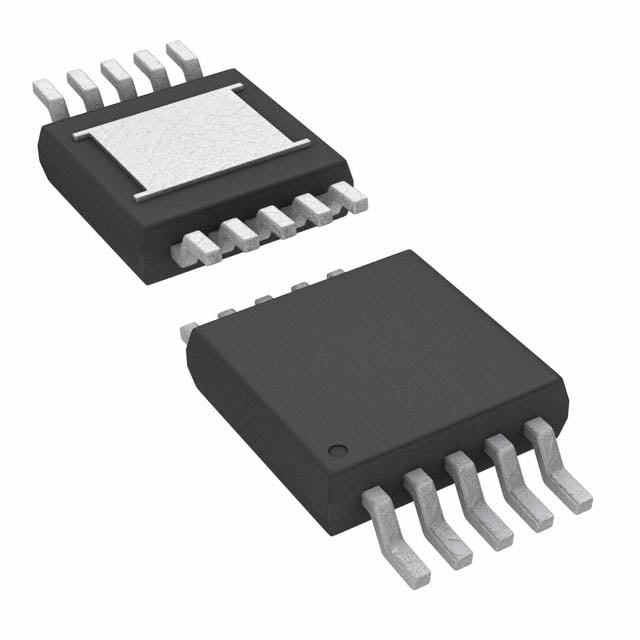
| 产品图片 |
|
| 产品型号 | LTC3255EMSE#PBF |
| PWM类型 | Burst Mode® |
| rohs | 无铅 / 符合限制有害物质指令(RoHS)规范要求 |
| 产品系列 | - |
| 供应商器件封装 | 10-MSOP-EP |
| 包装 | 管件 |
| 同步整流器 | 无 |
| 安装类型 | 表面贴装 |
| 封装/外壳 | 10-TFSOP,10-MSOP(0.118",3.00mm 宽)裸焊盘 |
| 工作温度 | -55°C ~ 150°C |
| 标准包装 | 50 |
| 电压-输入 | 4 V ~ 48 V |
| 电压-输出 | 2.4 V ~ 12.5 V |
| 电流-输出 | 50mA |
| 类型 | 降压(降压),切换电容(充电泵) |
| 输出数 | 1 |
| 输出类型 | 可调式 |
| 频率-开关 | 500kHz |


PDF Datasheet 数据手册内容提取
LTC3255 Wide V Range IN Fault Protected 50mA Step-Down Charge Pump FEATURES DESCRIPTION n Input Voltage Range: 4V to 48V The LTC®3255 is a switched-capacitor step-down DC/DC n Adjustable Regulated Output: 2.4V to 12.5V converter that produces a regulated output (2.4V to 12.5V n Output Current: 50mA Maximum adjustable) from a 4V to 48V input. In applications where n 16μA Quiescent Current in Regulation at No Load the input voltage exceeds twice the output voltage, 2:1 n Input Fault Protection from –52V to 60V capacitive charge pumping extends output current capabil- n Multimode Charge Pump (2:1, 1:1) with Automatic ity beyond input supply current limits. At no load, Burst Mode Switching Maintains Regulation Over Wide Mode® operation cuts V quiescent current to 16µA. IN V Range IN With its integrated V shunt regulator, the LTC3255 IN n Input Voltage Shunt Mode for Current-Fed Applications excels in 4mA to 20mA current loop applications. The n Power Good Output device enables current multiplication; a 4mA input current n Overtemperature and Short-Circuit Protection can power a 7.4mA load continuously. Alternatively, the n Operating Junction Temperature: 150°C Maximum LTC3255 serves as a higher efficiency replacement for n Thermally Enhanced 10-Lead MSOP and 10-Lead linear regulators and provides a space-saving inductor- (3mm × 3mm) DFN packages free alternative to buck DC/DC converters. APPLICATIONS The LTC3255 withstands reverse-polarity input supplies and output short-circuits without damage. Safety features n Industrial Control, Factory Automation, Sensors, and including current limit and overtemperature protection SCADA Systems further enhance robustness. The LTC3255 is available in n Housekeeping Power Supplies thermally enhanced 10-lead MSOP and low profile 3mm n Current-Boosting Voltage Regulators for 4mA to × 3mm 10-lead DFN packages. 20mA Current Loops L, LT, LTC, LTM, Linear Technology, the Linear logo and Burst Mode are registered trademarks and ThinSOT is a trademark of Linear Technology Corporation. All other trademarks are the property of their respective owners. TYPICAL APPLICATION Available Output Current 7.4mA DC Supply from 4mA to 20mA Current Loop vs Input Current 40 1µF 37 mA) 34 + VIN C+ C– VOUT O3.U3TVPUT RENT ( 3218 EN LTC3255PGOOD 22P0kGOOD 7.4mA UT CUR 2252 AVAILAIBOLUET IOUINT CCRAPEAASBEILDITY 4mA TO 20mA INPUT P >10V COMPLIANCE 1µF SHUNT 2.15M 10µF OUT 19 E 16 BIAS GND FB L B A 13 – 0.1µF 1.21M 3255 TA01a AVAIL 10 ICNUPRURTENT 7 4 4 6 8 10 12 14 16 18 20 INPUT CURRENT (mA) 3255 TA01b 3255f 1 For more information www.linear.com/LTC3255
LTC3255 ABSOLUTE MAXIMUM RATINGS (Notes 1, 2) V , EN ........................................................–52V to 60V I When V < 0V (Note 5) .....................100µA IN PGOOD PGOOD V ..........................................................................15V Operating Junction Temperature OUT V Short-Circuit Duration (Note 6) ...............Indefinite Range (Notes 3, 6) .................................–55°C to 150°C OUT I When V < 0V (Note 4) .............................50mA Storage Temperature Range ..................–65°C to 150°C VOUT OUT FB .............................................................................±6V Lead Temperature (Soldering, 10 sec) PGOOD ......................................................................15V MSE Only ..........................................................300°C PIN CONFIGURATION TOP VIEW TOP VIEW VOCU+T 21 11 190 CVI–N VOCU+T 12 11 190 VCI–N FB 3 GND 8 GND FB 3 GND 8 GND SHUNT 4 7 BIAS SHUNT 4 7 BIAS PGOOD 5 6 EN PGOOD 5 6 EN MSE PACKAGE 10-LEAD PLASTIC MSOP DD PACKAGE 10-LEAD (3mm × 3mm) PLASTIC DFN TJMAX = 150°C, θJA = 40°C/W EXPOSED PAD (PIN 11) IS GND, MUST BE SOLDERED TO PCB TJMAX = 150°C, θJA = 43°C/W EXPOSED PAD (PIN 11) IS GND, MUST BE SOLDERED TO PCB ORDER INFORMATION LEAD FREE FINISH TAPE AND REEL PART MARKING* PACKAGE DESCRIPTION TEMPERATURE RANGE LTC3255EDD#PBF LTC3255EDD#TRPBF LGHD 10-Lead (3mm × 3mm) Plastic DFN –40°C to 125°C LTC3255IDD#PBF LTC3255IDD#TRPBF LGHD 10-Lead (3mm × 3mm) Plastic DFN –40°C to 125°C LTC3255HDD#PBF LTC3255HDD#TRPBF LGHD 10-Lead (3mm × 3mm) Plastic DFN –40°C to 150°C LTC3255MPDD#PBF LTC3255MPDD#TRPBF LGHD 10-Lead (3mm × 3mm) Plastic DFN –55°C to 150°C LTC3255EMSE#PBF LTC3255EMSE#TRPBF LTGHF 10-Lead Plastic MSOP –40°C to 125°C LTC3255IMSE#PBF LTC3255IMSE#TRPBF LTGHF 10-Lead Plastic MSOP –40°C to 125°C LTC3255HMSE#PBF LTC3255HMSE#TRPBF LTGHF 10-Lead Plastic MSOP –40°C to 150°C LTC3255MPMSE#PBF LTC3255MPMSE#TRPBF LTGHF 10-Lead Plastic MSOP –55°C to 150°C Consult LTC Marketing for parts specified with wider operating temperature ranges. *The temperature grade is identified by a label on the shipping container. Consult LTC Marketing for information on nonstandard lead based finish parts. For more information on lead free part marking, go to: http://www.linear.com/leadfree/ For more information on tape and reel specifications, go to: http://www.linear.com/tapeandreel/ 3255f 2 For more information www.linear.com/LTC3255
LTC3255 ELECTRICAL CHARACTERISTICS The l denotes the specifications which apply over the specified operating junction temperature range, otherwise specifications are at T = 25°C. V = 12V unless otherwise noted. (Notes 2, 3) A IN SYMBOL PARAMETER CONDITIONS MIN TYP MAX UNITS V Input Voltage Range (Note 7) l 4 48 V IN V Output Voltage Range l 2.4 12.5 V OUT V V Undervoltage Lockout Threshold V Rising, SHUNT = GND 2.4 2.7 V UVLO_BK IN IN with Shunt Disabled Hysteresis, SHUNT = GND 50 mV V V Undervoltage Lockout Threshold V Rising, SHUNT= BIAS 5 5.7 V UVLO_SH IN IN with Shunt Enabled Hysteresis, SHUNT= BIAS 200 mV I V Quiescent Current VIN IN EN Low Shutdown 3 6 µA EN High, SHUNT = GND Enabled, Output in Regulation 16 35 µA EN High, SHUNT = BIAS Enabled, Output in Regulation 30 45 µA I Available Output Current VOUT Shunt Disabled SHUNT = GND l 50 mA Shunt Enabled SHUNT = BIAS, I = 4mA, V = 3.3V l 7.4 7.8 mA VIN OUT V Regulated Feedback Voltage l 1.176 1.200 1.224 V FB I FB Pin Leakage V = 1.3V ±10 nA FB FB V EN High Level Input Voltage l 1.4 V EN_VIH V EN Low Level Input Voltage l 0.4 V EN_VIL I EN Pin Input Current V = 12V 0 ±1 µA EN EN V = 0V 0 ±1 µA EN I V Current Limit 120 mA LIM OUT f Oscillator Frequency 500 kHz OSC V PGOOD Rising Threshold % of Final Regulation Voltage l 90 94 98 % PGTHRESH V PGOOD Output Low Voltage I = 200µA 0.1 0.4 V PG(LOW) PGOOD PGOOD High Impedance Leakage V = 12V l 1 µA PGOOD Note 1: Stresses beyond those listed under Absolute Maximum Ratings Note 4: The LTC3255 has an internal diode that conducts whenever VOUT may cause permanent damage to the device. Exposure to any Absolute is pulled below GND. When so pulled, absolute maximum current out of Maximum Rating condition for extended periods may affect device VOUT is 50mA. reliability and lifetime. Note 5: The LTC3255 has an internal diode that conducts whenever Note 2: All voltages are referenced to GND unless otherwise specified. PGOOD is pulled below GND. When so pulled, absolute maximum current out of PGOOD is 100µA. Note 3: The LTC3255E is guaranteed to meet performance specifications from 0°C to 85°C operating junction temperature. Specifications over Note 6: This IC has overtemperature protection that is intended to protect the –40°C to 125°C operating junction temperature range are assured by the device during momentary overload conditions. Junction temperatures design, characterization and correlation with statistical process controls. will exceed 150°C when overtemperature protection is active. Continuous The LTC3255I is guaranteed over the –40°C to 125°C operating junction operation above the specified maximum operating junction temperature temperature range. The LTC3255H is guaranteed over the –40°C to 150°C may impair device reliability. operating junction temperature range. The LTC3255MP is guaranteed over Note 7: This IC has input overvoltage protection that shuts down the the –55°C to 150°C operating junction temperature range. High junction device whenever V exceeds the specified input voltage range. Shutdown IN temperatures degrade operating lifetimes; operating lifetime is derated typically occurs when V exceeds 52V. V subsequently must fall below IN IN for junction temperatures greater than 125°C. Note that the maximum 50V (typical) for the IC to re-enable. ambient temperature consistent with these specifications is determined by specific operating conditions in conjunction with board layout, the rated package thermal resistance and other environmental factors. The junction temperature (T , in °C) is calculated from the ambient J temperature (T , in °C) and power dissipation (P , in Watts) according to A D the formula: TJ = TA + (PD • θJA) where θJA (in °C/W) is the package thermal impedance. 3255f 3 For more information www.linear.com/LTC3255
LTC3255 TYPICAL PERFORMANCE CHARACTERISTICS T = 25°C, unless otherwise noted. A Input Operating Current Input Operating Current Input Shutdown Current vs Input Voltage vs Temperature vs Input Voltage 50 50 30 45 SVHOUUTN =T 5=V GND 45 VVIONU =T =1 25VV EN = GND 40 TA = 25°C 40 SHUNT = GND 25 35 35 20 I (µA)VIN 223050 I (µA)VIN 223050 I (µA)VIN 15 150°C 10 125°C 15 15 25°C 10 10 5 5 5 –55°C 0 0 0 5 10 15 20 25 30 35 40 45 50 –60 –30 0 30 60 90 120 150 0 10 20 30 40 50 60 VIN (V) TEMPERATURE (°C) VIN (V) 3255 G01 3255 G02 3255 G03 FB Pin Regulation Voltage FB Pin Regulation Voltage FB Pin Regulation Voltage vs Input Voltage (I = 1mA) vs Input Voltage (I = 50mA) vs Temperature OUT OUT 1.224 1.224 1.224 1.220 IVOOUUTT = = 1 5mVA 1.220 IVOOUUTT = = 5 50VmA 1.220 VIOINU T= = 1 12mVA 1.216 SHUNT = GND 1.216 SHUNT = GND 1.216 VOUT = 5V 1.212 1.212 1.212 1.208 1.208 1.208 V (V)FB111...221009406 V (V)FB111...221009406 V (V)FB111...212090064 1.192 1.192 1.192 1.188 –60°C 1.188 1.188 1.184 25°C 1.184 –60°C 1.184 105°C 25°C 1.180 150°C 1.180 105°C 1.180 1.176 1.176 1.176 5 10 15 20 25 30 35 40 45 50 5 10 15 20 25 30 35 40 45 50 –60 –30 0 30 60 90 120 150 VIN (V) VIN (V) TEMPERATURE (°C) 3255 G04 3255 G05 3255 G06 Operating Mode Transition Operating Mode Transition Typical Minimum V – 2 • V IN OUT Voltage vs Input Voltage Voltage vs Input Voltage Compliance Required for Shunt (I = 5mA) (I = 50mA) Mode Operation OUT OUT 25 25 3.5 SHUNT = GND SHUNT = GND IVIN = 20mA 23 23 3.4 21 21 3.3 19 19 3.2 2:1 MODE V) V) 17 2:1 MODE V) 17 (OUT3.1 V (IN 15 1:1 MODE V (IN 15 1:1 MODE 2 • V 3.0 13 • 13 • – N2.9 11 TRANSITION 11 TRANSITION VI2.8 9 REGION 9 REGION 2.7 VVOOUUTT == 23..53VV 7 7 2.6 VOUT = 5V VOUT = 12V 5 5 2.5 2 3 4 5 6 7 8 9 10 11 12 2 3 4 5 6 7 8 9 10 11 12 –60 –30 0 30 60 90 120 150 VOUT (V) VOUT (V) TEMPERATURE (°C) 3255 G07 3255 G08 3255 G09 3255f 4 For more information www.linear.com/LTC3255
LTC3255 TYPICAL PERFORMANCE CHARACTERISTICS T = 25°C, unless otherwise noted. A 3.3V Efficiency 5V Efficiency 5V Efficiency OUT OUT OUT vs Input Voltage at 50mA Load vs Input Voltage at 50mA Load vs Output Current 100 100 90 120 SHUNT = GND SHUNT = GND VIN = 12V 90 90 EFFICIENCY 80 100 80 80 P NCY (%) 7600 LTC3255 NCY (%) 6700 LTC3255 NCY (%) 7600 8600 OWER LO EFFICIE 5400 EFFICIE 4500 EFFICIE 50 40 SS (mW IDEAL LDO IDEAL LDO ) 30 30 40 20 20 20 POWER LOSS 10 10 30 0 4 6 8 10 12 14 16 18 20 5 7 9 11 13 15 17 19 21 23 25 0.1 1 10 100 INPUT VOLTAGE (V) INPUT VOLTAGE (V) OUTPUT CURRENT (mA) 3255 G16 3255 G17 3255 G18 2.5V Output Voltage Output Ripple vs Falling Input Voltage Load Transient 2.55 SHUNT = GND 2.54 IOUT = 50mA 2.53 VOUT 2.52 VOUT 50mV/DIV 20mV/DIV AC-COUPLED V)2.51 AC-COUPLED (UT2.50 O V2.49 50mA IOUT 2.48 5mA 2.47 –60°C VVIONU =T =1 23V.3V 40µs/DIV 3255 G10 VIN = 12V 40µs/DIV 3255 G11 2.46 2152°5C°C IOUT = 5mA VOUT = 3.3V 2.45 2 3 4 5 6 7 8 9 10 VIN (V) 3255 G12 3.3V Output Voltage 5V Output Voltage 12V Output Voltage vs Falling Input Voltage vs Falling Input Voltage vs Falling Input Voltage 3.40 5.10 12.25 SHUNT = GND SHUNT = GND SHUNT = GND 3.38 IOUT = 50mA 5.08 IOUT = 50mA 12.20 IOUT = 50mA 3.36 5.06 12.15 3.34 5.04 12.10 V (V)OUT333...323280 V (V)OUT545...090280 V (V)OUT111212...090550 3.26 4.96 11.90 3.24 –60°C 4.94 –60°C 11.85 –60°C 3.22 25°C 4.92 25°C 11.80 25°C 125°C 125°C 125°C 3.20 4.90 11.75 2 3 4 5 6 7 8 9 10 11 12 4 5 6 7 8 9 10 11 12 13 14 15 10 12 14 16 18 20 22 24 26 28 30 VIN (V) VIN (V) VIN (V) 3255 G13 3255 G14 3255 G15 3255f 5 For more information www.linear.com/LTC3255
LTC3255 PIN FUNCTIONS C+ (Pin 1): Flying Capacitor Positive Connection. This pin EN (Pin 6): Logic Input. A logic high on the EN pin will must not be driven externally. enable the charge pump. A logic low shuts down the LTC3255. Do not float this pin. V (Pin 2): Charge Pump Output Voltage. OUT BIAS (Pin 7): Connect this pin to a 0.1µF bypass capaci- FB (Pin 3): Feedback pin for setting the regulated output tor to GND. A ceramic capacitor of at least 10V rating is voltage, usually connected to V through an external OUT recommended. resistor divider. In operation, the LTC3255 servos the FB pin to 1.2V by transferring charge from V to V . GND (Pin 8 and Exposed Pad Pin 11): Ground Connection. IN OUT Exposed pad (Pin 11) must be soldered to the circuit board SHUNT (Pin 4): Configuration pin that must connect to ground plane for proper thermal and electrical conduction. either the BIAS or GND pins to enable or defeat, respec- tively, the LTC3255’s shunt regulator feature. Connect this C– (Pin 9): Flying Capacitor Negative Connection. This pin pin to either BIAS or GND on the circuit board layout. Do must not be driven externally. not float this pin. V (Pin 10): Input Supply Voltage. Bypass this pin to GND IN PGOOD (Pin 5): Power Good Open-Drain Logic Output. with at least 1µF capacitance. This pin becomes high impedance when the feedback voltage on the FB pin rises above 94% (typical) of the regulation voltage. 3255f 6 For more information www.linear.com/LTC3255
LTC3255 SIMPLIFIED BLOCK DIAGRAM VIN 10 INTERNAL BIAS 7 BIASING C+ VOUT 1 2 C– 9 SHUNT CONTROL SHUNT 4 + FB 3 EN CHARGE 6 PUMP CONTROL – 1.2V PGOOD 5 – + 1.13V GND GND 8 11 3255 BD 3255f 7 For more information www.linear.com/LTC3255
LTC3255 APPLICATIONS INFORMATION General Operation Regulation Loop The LTC3255 uses switched-capacitor-based DC/DC Regulation is achieved via a Burst Mode control loop that conversion to provide efficiency advantages associated allows the LTC3255 to achieve high efficiency even at with inductor-based circuits together with the cost and light loads. As shown in the Block Diagram, a comparator simplicity advantages of linear regulators. No inductors monitors the output voltage via a feedback pin, FB, which are required. The LTC3255 uses an internal switch network receives a fraction of V via an external resistor divider. OUT and fractional conversion ratios to achieve high efficiency While V is below regulation, the LTC3255 transfers fixed FB and regulation over widely varying V and output load packets of charge from V to V , paced by an internal IN IN OUT conditions. A defeatable V shunt regulator allows the oscillator. This causes V and hence FB to rise. When IN OUT LTC3255 to operate with current-fed V supplies, such V enters regulation, the LTC3255 stops charge transfer IN FB as 4mA to 20mA current loops. and enters a low quiescent current sleep state. During this sleep state, the output load is supplied entirely by the output Automatic 2:1/1:1 Mode Switching with VIN Shunt capacitor. The LTC3255 remains in sleep until the output Disabled (SHUNT Pin Connected to GND) drops enough to require another burst of charge. As load current decreases, the output capacitor takes longer to Connecting the SHUNT pin to GND defeats the V shunt IN discharge, so sleep time increases. regulator. With the shunt regulator defeated, the LTC3255 functions as a general purpose step-down charge pump Shutdown and Undervoltage Lockout (UVLO) offering two conversion modes: 2:1 and 1:1. Internal cir- cuitry automatically chooses the optimal conversion ratio Driving the EN pin low puts the LTC3255 in shutdown, based on V , V , and output load conditions, generally which disables all circuitry except the internal bias. V IN OUT IN preferring 2:1 mode when V exceeds twice V , but supply current is minimized. When the EN pin is high, the IN OUT falling back to 1:1 mode as needed to maintain regulation. charge pump will enable if V satisfies the V undervolt- IN IN age lockout (UVLO) threshold. If the shutdown feature is Forced 2:1 Mode Operation When VIN Shunt Regulator not needed, the EN pin can be connected to VIN, as both is Enabled (SHUNT Pin Connected to BIAS) pins share the same Absolute Maximum rating. With the SHUNT pin connected to BIAS, the V shunt IN Reverse Polarity Input Protection regulator is enabled, and the LTC3255 expects a high impedance power source at V , such as a 4mA to 20mA The V and EN pins are designed to withstand connection IN IN current loop, or a resistor to a DC supply. With the shunt to voltages below ground without damage. When V is IN regulator enabled, the charge pump runs in 2:1 conversion below ground, the LTC3255 prevents V from going more OUT mode only, extending its output current capability beyond than a diode drop below GND to protect the load circuit. that of the V source. For example, the LTC3255 can IN typically boost the current capability of a 4mA source to Short-Circuit/Thermal Protection power a 7.4mA load continuously. See V Shunt Regula- IN The LTC3255 has built-in short-circuit current limiting as tor in the Operation section for V compliance and other IN well as overtemperature protection. During short-circuit operating information. conditions output current is automatically limited by the output current limit circuitry. 3255f 8 For more information www.linear.com/LTC3255
LTC3255 APPLICATIONS INFORMATION The LTC3255 has thermal protection that will shut 2:1 Step-Down Charge Pump Operation down the device if the junction temperature exceeds the In 2:1 step-down mode, charge transfer from V to V IN OUT overtemperature threshold (typically 175°C). Thermal happens in two phases. On the first phase, the flying ca- shutdown is included to protect the IC in cases of exces- pacitor (C ) is connected between V and V . On this FLY IN OUT sively high ambient temperatures, or in cases of excessive phase C is charged up and current is delivered to V . FLY OUT power dissipation inside the IC. The charge transfer will On the second phase, C is connected between V and FLY OUT reactivate once the junction temperature drops back to GND. The charge stored on C during the first phase is FLY approximately 165°C. transferred to V on the second phase. When in 2:1 OUT When the thermal protection is active, the junction tem- step-down mode, the input current will be approximately perature is beyond the specified operating range. Thermal half of the total output current. The efficiency (η) and chip protection is intended for momentary overload conditions power dissipation (P ) in 2:1 mode are approximately: D outside normal operation. Continuous operation above the P V •I 2V specified maximum operating junction temperature may η= OUT = OUT OUT = OUT P 1 V impair device reliability. IN V • I IN IN OUT 2 Programming the Output Voltage (FB Pin) V PD= 2IN –VOUTIOUT The LTC3255 output voltage is set by connecting its FB pin to a resistor divider between V and GND as shown OUT in Figure 1. 1:1 Step-Down Charge Pump Operation The desired adjustable output voltage is programmed by 1:1 step-down mode is similar to how a linear regulator solving the following equation for R and R : works. Charge is delivered directly from V to V through A B IN OUT most of the internal oscillator period. The charge transfer R V A = OUT –1 is briefly interrupted at the end of the period. When in 1:1 R 1.2V B step-down mode the input current will be approximately equal to the total output current. Thus efficiency (η) and Select a value for R in the range of 20k to 2M and solve B chip power dissipation (P ) in 1:1 mode are approximately: for R . Note that the resistor divider current adds to the D A total no-load operating current. Thus a larger value for R P V •I V B η= OUT = OUT OUT = OUT will result in lower operating current. P V •I V IN IN OUT IN P =(V –V )I D IN OUT OUT ( ) VOUT VOUT =1.2V1 +RA RB LTC3255 RA FB COUT RB GND 3255 F01 Figure 1. Setting the Output Voltage 3255f 9 For more information www.linear.com/LTC3255
LTC3255 APPLICATIONS INFORMATION Power Good Output Operation (PGOOD) where I is the time-averaged current being fed into V IN IN by the current loop, V is the output voltage, and I The LTC3255 includes an open-drain power good (PGOOD) OUT OUT is the output load current. Notice that the largest power output pin. If the chip is in shutdown or undervoltage dissipation occurs when output load current is zero. This lockout, or if the FB pin voltage is less than 90% (typi- is because any power fed into V must be dissipated in cal) of its regulation voltage, PGOOD is low impedance IN either the load or the LTC3255. If the load is not drawing to ground. PGOOD becomes high impedance when V OUT any current, then the LTC3255 must dissipate all of the rises to 94% (typical) of its regulation voltage. PGOOD input power. stays high impedance until V is shut down or drops OUT below the PGOOD falling threshold (90% typical). A pull- When the shunt regulator is enabled, the LTC3255 charge up resistor can be inserted between PGOOD and V to pump is locked in 2:1 mode. To achieve output regulation, OUT signal a valid power good condition. The use of a large the input current to the part must have sufficient voltage value pull-up resistor on PGOOD and a capacitor placed compliance above twice V . The graph in Figure 2 shows OUT between PGOOD and GND can be used to delay the PGOOD the typical minimum compliance required at the V pin IN signal if desired. for correct operation. For V ≤ 5.5V, a V compliance OUT IN of 2V + 3.5V is recommended. For V > 5.5V, a V OUT OUT IN VIN Shunt Regulator Operation compliance of 2VOUT + 4V is recommended. The V shunt regulator feature of the LTC3255 is intended IN 3.5 for applications where VIN is current-fed, such as in 4mA 3.4 IVIN = 20mA to 20mA current loops. A circuit powered by a current 3.3 loop must limit the voltage drop it presents to the loop to 3.2 avoid exceeding the loop compliance, which would break (V)UT3.1 ttohres c uVrIrNe nant ldo oVpO.U TTh, ed LrTawC3in2g5 5V’IsN V cINu rsrheunnt ta rse gnuelcaetosrs maroy ntio- – 2 • VNO23..90 keep VIN from rising much beyond 3V above twice VOUT. VI2.8 2.7 VOUT = 2.5V The shunt regulator is enabled by connecting the SHUNT VOUT = 3.3V 2.6 VOUT = 5V pin to the BIAS pin in the circuit board layout. The shunt VOUT = 12V 2.5 is disabled by connecting the SHUNT pin to GND. –60 –30 0 30 60 90 120 150 TEMPERATURE (°C) The shunt regulator dissipates power which must be ac- 3255 F02 counted for in thermal budgeting. Total power dissipation Figure 2. Typical Minimum V – 2 • V Compliance Required IN OUT (P ) in the LTC3255 with shunt regulator enabled is for Shunt Mode Operation DSHUNT equal to the input power minus the output power of the LTC3255, or approximately: P =P –P D(SHUNT) IN OUT =V •I –V •I IN IN OUT OUT ≈(2•V +2V)•I –V •I OUT IN OUT OUT 3255f 10 For more information www.linear.com/LTC3255
LTC3255 APPLICATIONS INFORMATION V Ripple and Capacitor Selection Flying Capacitor Selection OUT The type and value of capacitors used with the LTC3255 The flying capacitor should always be a ceramic type. determine several important parameters such as output Polarized capacitors such as tantalum or aluminum electro- ripple and charge pump strength. The value of C lytics are not recommended. The flying capacitor controls OUT directly controls the amount of output ripple for a given the strength of the charge pump. In order to achieve the load current. Increasing the size of C will reduce the rated output current, it is necessary for the flying capaci- OUT output ripple. tor to have at least 0.4μF of capacitance over operating temperature with a bias voltage equal to the programmed To reduce output noise and ripple, it is suggested that a V (see Ceramic Capacitor Selection Guidelines). The low ESR (equivalent series resistance < 0.1Ω) ceramic OUT voltage rating of the ceramic capacitor should be V + capacitor (10μF or greater) be used for C . Ceramic OUT OUT 1V or greater. capacitors typically have exceptionally low ESR which, combined with a tight board layout, should yield excellent Ceramic Capacitor Selection Guidelines performance. Tantalum and aluminum capacitors can be Capacitors of different materials lose their capacitance used in parallel with a ceramic capacitor to increase the with higher temperature and voltage at different rates. total capacitance but are not recommended to be used For example, a ceramic capacitor made of X5R or X7R alone because of their high ESR. material will retain most of its capacitance from –40°C V Capacitor Selection to 85°C, whereas a Z5U or Y5V style capacitor will lose IN considerable capacitance over that range (60% to 80% The total amount and type of capacitance necessary for loss typical). Z5U and Y5V capacitors may also have a input bypassing is very dependent on the impedance of very strong voltage coefficient, causing them to lose an the input power source as well as existing bypassing al- additional 60% or more of their capacitance when the rated ready on the V node. For optimal input noise and ripple IN voltage is applied. Therefore, when comparing different reduction, it is recommended that a low ESR ceramic capacitors, it is often more appropriate to compare the capacitor be used for C bypassing. Low ESR will reduce IN amount of achievable capacitance for a given case size the voltage steps caused by changing input current, while rather than discussing the specified capacitance value. For the absolute capacitor value will determine the level of example, over rated voltage and temperature conditions, ripple. An electrolytic or tantalum capacitor may be used a 4.7μF, 10V, Y5V ceramic capacitor in an 0805 case may in parallel with the ceramic capacitor on C to increase IN not provide any more capacitance than a 1μF, 10V, X5R the total capacitance, but due to the higher ESR, it is not or X7R available in the same 0805 case. In fact, over bias recommended that an electrolytic or tantalum capacitor be and temperature range, the 1μF, 10V, X5R or X7R will used alone for input bypassing. The LTC3255 will operate provide more capacitance than the 4.7μF, 10V, Y5V. The with capacitors less than 1μF, but depending on the source capacitor manufacturer’s data sheet should be consulted impedance, input noise can feed through to the output to determine what value of capacitor is needed to ensure causing degraded performance. For best performance, minimum capacitance values are met over operating 1μF or greater total capacitance is suggested for C . IN temperature and bias voltage. Table 1 is a list of ceramic capacitor manufacturers in alphabetical order: 3255f 11 For more information www.linear.com/LTC3255
LTC3255 APPLICATIONS INFORMATION large ground plane under the device can reduce the thermal Table 1 resistance of the package and PC board considerably. Poor CERAMIC CAPACITOR MANUFACTURER WEBSITE board layout and failure to connect the die paddle (Pin AVX www.avxcorp.com 11) to a large ground plane can result in thermal junction Kemet www.kemet.com to ambient impedance well in excess of 40°C/W (MSE Murata www.murata.com package) or in excess of 43°C/W (DD package). Thermal Taiyo Yuden www.t-yuden.com junction to ambient impedance is specified per JEDEC TDK www.tdk.com standard JESD 51-5. Layout Considerations Because of the wide input operating range it is possible to Due to the high switching frequency and transient cur- exceed the specified operating junction temperature and rents produced by the LTC3255, careful board layout is even reach thermal shutdown. It is the responsibility of necessary for optimal performance. A true ground plane the user of the LTC3255 to calculate worst-case operat- and short connections to all capacitors will optimize ing conditions (temperature and power) to make sure performance, reduce noise and ensure proper regulation the LTC3255’s specified operating junction temperature over all conditions. is not exceeded for extended periods of time. The 2:1 Step-Down, 1:1 Step-Down, and V Shunt Regulator When using the LTC3255 with an external resistor divider IN Operation sections provide equations for calculating the it is important to minimize any stray capacitance to the FB power dissipation (P ) in each mode. node. Stray capacitance from FB to C+ or C– can degrade D performance significantly and should be minimized and/ For example, if it is determined that the maximum power or shielded if necessary. dissipation (P ) is 1.2W under normal operation, then D the maximum junction to ambient temperature rise in the Thermal Management MSE package will be: The on chip power dissipation in the LTC3255 will cause Junction to Ambient = 1.2W • 40°C/W = 48°C the junction to ambient temperature to rise at a rate of Thus, the ambient temperature under this condition can 40°C/W or more in the MSE package, or 43°C/W or more not exceed 102°C if the junction temperature is to remain in the DD package. To reduce the maximum junction below 150°C. For ambient temperatures exceeding roughly temperature, a good thermal connection to the PC board 127°C, the device will cycle in and out of the thermal is recommended. Connecting the die paddle (Pin 11) to a shutdown. 3255f 12 For more information www.linear.com/LTC3255
LTC3255 TYPICAL APPLICATIONS Wide Input Range 5V Microcontroller Supply (with Power-On Reset Delay) 1µF 6V TION P4U8VT VIN C+ C– VOUT VOUT = 5V VDD 1µF EN LTC3255 383k 510k 10µF µCONTROLLER BIAS FB 0.1µF PGOOD RESET SHUNT GND 121k 1µF GND 3255 TA02 7mA 5V Supply from 4mA to 20mA Current Loop 1µF + VIN C+ C– VOUT O5VUTPUT 7mA EN LTC3255 383k 220k FB 10µF 4mA TO 20mA INPUT 1µF 13.5V COMPLIANCE BIAS PGOOD PGOOD SHUNT GND 121k 0.1µF – 3255 TA03 3255f 13 For more information www.linear.com/LTC3255
LTC3255 PACKAGE DESCRIPTION Please refer to http://www.linear.com/designtools/packaging/ for the most recent package drawings. DD Package 10-Lead Plastic DFN (3mm × 3mm) (Reference LTC DWG # 05-08-1699 Rev C) 0.70 ±0.05 3.55 ±0.05 1.65 ±0.05 2.15 ±0.05 (2 SIDES) PACKAGE OUTLINE 0.25 ± 0.05 0.50 BSC 2.38 ±0.05 (2 SIDES) RECOMMENDED SOLDER PAD PITCH AND DIMENSIONS R = 0.125 0.40 ± 0.10 TYP 6 10 3.00 ±0.10 1.65 ± 0.10 (4 SIDES) (2 SIDES) PIN 1 NOTCH PIN 1 R = 0.20 OR TOP MARK 0.35 × 45° (SEE NOTE 6) CHAMFER (DD) DFN REV C 0310 5 1 0.200 REF 0.75 ±0.05 0.25 ± 0.05 0.50 BSC 2.38 ±0.10 (2 SIDES) 0.00 – 0.05 BOTTOM VIEW—EXPOSED PAD NOTE: 1. DRAWING TO BE MADE A JEDEC PACKAGE OUTLINE M0-229 VARIATION OF (WEED-2). CHECK THE LTC WEBSITE DATA SHEET FOR CURRENT STATUS OF VARIATION ASSIGNMENT 2. DRAWING NOT TO SCALE 3. ALL DIMENSIONS ARE IN MILLIMETERS 4. DIMENSIONS OF EXPOSED PAD ON BOTTOM OF PACKAGE DO NOT INCLUDE MOLD FLASH. MOLD FLASH, IF PRESENT, SHALL NOT EXCEED 0.15mm ON ANY SIDE 5. EXPOSED PAD SHALL BE SOLDER PLATED 6. SHADED AREA IS ONLY A REFERENCE FOR PIN 1 LOCATION ON THE TOP AND BOTTOM OF PACKAGE 3255f 14 For more information www.linear.com/LTC3255
LTC3255 PACKAGE DESCRIPTION Please refer to http://www.linear.com/designtools/packaging/ for the most recent package drawings. MSE Package 10-Lead Plastic MSOP, Exposed Die Pad (Reference LTC DWG # 05-08-1664 Rev I) BOTTOM VIEW OF EXPOSED PAD OPTION 1.88 1.88 ±0.102 (.074 ±.004) 0.889 ±0.127 1 (.074) 0.29 (.035 ±.005) 1.68 REF (.066) 5.10 0.05 REF 1.68 ±0.102 3.20 – 3.45 (.201) DETAIL “B” (.066 ±.004) (.126 – .136) MIN CORNER TAIL IS PART OF DETAIL “B” THE LEADFRAME FEATURE. FOR REFERENCE ONLY 10 NO MEASUREMENT PURPOSE 0.50 0.305 ± 0.038 (.0197) 3.00 ±0.102 (.0120 ±.0015) BSC (.118 ±.004) 0.497 ±0.076 TYP (NOTE 3) (.0196 ±.003) RECOMMENDED SOLDER PAD LAYOUT 10 9 8 76 REF 3.00 ±0.102 4.90 ±0.152 (.118 ±.004) (.193 ±.006) (NOTE 4) DETAIL “A” 0.254 (.010) 0° – 6° TYP GAUGE PLANE 1 2 3 4 5 0.53 ±0.152 1.10 0.86 (.021 ±.006) (.043) (.034) MAX REF DETAIL “A” 0.18 (.007) SEATING PLANE 0.17 – 0.27 0.1016 ±0.0508 (.007 – .011) (.004 ±.002) 0.50 TYP (.0197) MSOP (MSE) 0213 REV I NOTE: BSC 1. DIMENSIONS IN MILLIMETER/(INCH) 2. DRAWING NOT TO SCALE 3. DIMENSION DOES NOT INCLUDE MOLD FLASH, PROTRUSIONS OR GATE BURRS. MOLD FLASH, PROTRUSIONS OR GATE BURRS SHALL NOT EXCEED 0.152mm (.006") PER SIDE 4. DIMENSION DOES NOT INCLUDE INTERLEAD FLASH OR PROTRUSIONS. INTERLEAD FLASH OR PROTRUSIONS SHALL NOT EXCEED 0.152mm (.006") PER SIDE 5. LEAD COPLANARITY (BOTTOM OF LEADS AFTER FORMING) SHALL BE 0.102mm (.004") MAX 6. EXPOSED PAD DIMENSION DOES INCLUDE MOLD FLASH. MOLD FLASH ON E-PAD SHALL NOT EXCEED 0.254mm (.010") PER SIDE. 3255f 15 Information furnished by Linear Technology Corporation is believed to be accurate and reliable. However, no responsibility is assumed for its use. Linear Technology Corporation makes no representa- tion that the interconneFcotior nm oof irtse ciinrcfouirtms aast dioensc wribwedw h.leirneeina rw.cilol nmot/ LinTfCrin3g2e5 o5n existing patent rights.
LTC3255 TYPICAL APPLICATION Wide Input Range 12V Supply 1µF INPUT C+ C– OUTPUT 13V TO 48V VIN VOUT 12V 50mA EN LTC3255 1.1M 220k 1µF 10µF BIAS FB 0.1µF PGOOD PGOOD SHUNT GND 121k 3255 TA04 RELATED PARTS PART NUMBER DESCRIPTION COMMENTS LTC1751-3.3/LTC1751-5 100mA, 800kHz Regulated Doubler V : 2V to 5V, V = 3.3V/5V, I = 20μA, I < 2μA, IN OUT(MAX) Q SD MS8 Package LTC1983-3/LTC1983-5 100mA, 900kHz Regulated Inverter V : 3.3V to 5.5V, V = –3V/–5V, I = 25μA, I < 2μA, IN OUT(MAX) Q SD ThinSOT™ Package LTC3200-5 100mA, 2MHz Low Noise, Doubler/White LED Driver V : 2.7V to 4.5V, V = 5V, I = 3.5mA, I < 1μA, IN OUT(MAX) Q SD ThinSOT Package LTC3202 125mA, 1.5MHz Low Noise, Fractional White LED Driver V : 2.7V to 4.5V, V = 5.5V, I = 2.5mA, I < 1μA, IN OUT(MAX) Q SD DFN, MS Packages LTC3204-3.3/LTC3204B-3.3 Low Noise, Regulated Charge Pumps in (2mm × 2mm) VIN: 1.8V to 4.5V (LTC3204B-3.3), 2.7V to 5.5V (LTC3204B-5), LTC3204-5/LTC3204B-5 DFN Package IQ = 48μA, LTC3204B Version without Burst Mode Operation, 6-Lead (2mm × 2mm) DFN Package LTC3440 600mA (I ) 2MHz Synchronous Buck-Boost DC/DC 95% Efficiency, V : 2.5V to 5.5V, V = 2.5V, I = 25μA, OUT IN OUT(MIN) Q Converter I ≤ 1μA, 10-Lead MS Package SD LTC3441 High Current Micropower 1MHz Synchronous 95% Efficiency, V : 2.5V to 5.5V, V = 2.5V, I = 25μA, IN OUT(MIN) Q Buck-Boost DC/DC Converter I ≤ 1μA, DFN Package SD LTC3443 High Current Micropower 600kHz Synchronous 96% Efficiency, V : 2.4V to 5.5V, V = 2.4V, I = 28μA, IN OUT(MIN) Q Buck-Boost DC/DC Converter I < 1μA, DFN Package SD LTC3240-3.3/ 3.3V/2.5V Step-Up/Step-Down Charge Pump DC/DC V : 1.8V to 5.5V, V = 3.3V/2.5V, I = 65μA, I < 1μA, IN OUT(MAX) Q SD LTC3240-2.5 Converter (2mm × 2mm) DFN Package LTC3245 Wide V Range Low Noise 250mA Buck-Boost V : 2.7V to 38V, V = 5V, I = 20µA, I = 4µA, IN IN OUT(MAX) Q SD Charge Pump 12-Lead MS and (3mm × 4mm) DFN Packages LTC3260 Low Noise Dual Supply Inverting Charge Pump Inverting Charge Pump With Integrated Dual Polarity 50mA LDO Post-Regulated Outputs. V : 4.5V to 32V, Charge Pump V : IN OUT –0.94 • V , 100mA IN LTC3261 High Voltage, Low Quiescent Current Inverting V : 4.5V to 32V, V = –V , I = 100mA, MSOP-12 Package IN OUT IN OUT Charge Pump 3255f 16 Linear Technology Corporation LT 0813 • PRINTED IN USA 1630 McCarthy Blvd., Milpitas, CA 95035-7417 For more information www.linear.com/LTC3255 (408) 432-1900 ● FAX: (408) 434-0507 ● www.linear.com/LTC3255 LINEAR TECHNOLOGY CORPORATION 2013