ICGOO在线商城 > 集成电路(IC) > PMIC - 稳压器 - DC DC 开关稳压器 > LTC3221EDC#TRMPBF

 Datasheet下载
- 型号: LTC3221EDC#TRMPBF
- 制造商: LINEAR TECHNOLOGY
- 库位|库存: xxxx|xxxx
- 要求:
| 数量阶梯 | 香港交货 | 国内含税 |
| +xxxx | $xxxx | ¥xxxx |
查看当月历史价格
查看今年历史价格
LTC3221EDC#TRMPBF产品简介:
ICGOO电子元器件商城为您提供LTC3221EDC#TRMPBF由LINEAR TECHNOLOGY设计生产,在icgoo商城现货销售,并且可以通过原厂、代理商等渠道进行代购。 LTC3221EDC#TRMPBF价格参考。LINEAR TECHNOLOGYLTC3221EDC#TRMPBF封装/规格:PMIC - 稳压器 - DC DC 开关稳压器, Charge Pump Switching Regulator IC Positive Adjustable 1.23V 1 Output 60mA 6-WFDFN Exposed Pad。您可以下载LTC3221EDC#TRMPBF参考资料、Datasheet数据手册功能说明书,资料中有LTC3221EDC#TRMPBF 详细功能的应用电路图电压和使用方法及教程。
LTC3221EDC#TRMPBF是由Linear Technology(现为Analog Devices旗下品牌)推出的一款开关稳压器,属于PMIC中的DC-DC开关稳压器类别。该器件集成了电荷泵和低压差线性稳压器(LDO),可提供高效的电压转换,适用于对空间和功耗敏感的便携式电子设备。

其典型应用场景包括:
1. 便携式医疗设备:如血糖仪、便携式监护仪等,因其低噪声、高效率和小尺寸封装,适合电池供电且要求长时间运行的设备。
2. 工业传感器与仪表:在4-20mA环路供电系统中,LTC3221EDC#TRMPBF可高效生成所需的偏置电压,同时保持低功耗和高稳定性。
3. 消费类电子产品:如智能手表、可穿戴设备和TWS耳机,利用其超小型DFN封装和低静态电流特性,延长电池续航时间。
4. 通信模块:用于为低功耗无线模块(如蓝牙、ZigBee、LoRa)提供稳定的双路输出电压,确保信号处理电路的可靠运行。

该芯片支持宽输入电压范围(2.7V至5.5V),可由单节锂电池或USB电源直接供电,内置软启动功能以减少浪涌电流,提升系统启动可靠性。其无电感电荷泵设计简化了外围电路,降低了EMI干扰,特别适合高密度PCB布局。

综上,LTC3221EDC#TRMPBF广泛应用于需要高效、紧凑、低噪声电源解决方案的便携式和低功耗系统中。
| 参数 | 数值 |
| 产品目录 | 集成电路 (IC) |
| 描述 | IC REG SWITCHED CAP DBL ADJ 6DFN |
| 产品分类 | |
| 品牌 | Linear Technology |
| 数据手册 | http://www.linear.com/docs/17438 |
| 产品图片 |
|
| 产品型号 | LTC3221EDC#TRMPBF |
| PWM类型 | Burst Mode® |
| rohs | 无铅 / 符合限制有害物质指令(RoHS)规范要求 |
| 产品系列 | - |
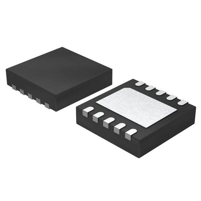
| 供应商器件封装 | 6-DFN(2x2) |
| 其它名称 | LTC3221EDC#TRMPBFDKR |
| 包装 | Digi-Reel® |
| 同步整流器 | 无 |
| 安装类型 | 表面贴装 |
| 封装/外壳 | 6-WFDFN 裸露焊盘 |
| 工作温度 | -40°C ~ 85°C |
| 标准包装 | 1 |
| 电压-输入 | 1.8 V ~ 5.5 V |
| 电压-输出 | 1.23V |
| 电流-输出 | 60mA |
| 类型 | 切换式电容器(充电泵),倍增器 |
| 输出数 | 1 |
| 输出类型 | 可调式 |
| 频率-开关 | 600kHz |


- 商务部:美国ITC正式对集成电路等产品启动337调查
- 曝三星4nm工艺存在良率问题 高通将骁龙8 Gen1或转产台积电
- 太阳诱电将投资9.5亿元在常州建新厂生产MLCC 预计2023年完工
- 英特尔发布欧洲新工厂建设计划 深化IDM 2.0 战略
- 台积电先进制程称霸业界 有大客户加持明年业绩稳了
- 达到5530亿美元!SIA预计今年全球半导体销售额将创下新高
- 英特尔拟将自动驾驶子公司Mobileye上市 估值或超500亿美元
- 三星加码芯片和SET,合并消费电子和移动部门,撤换高东真等 CEO
- 三星电子宣布重大人事变动 还合并消费电子和移动部门
- 海关总署:前11个月进口集成电路产品价值2.52万亿元 增长14.8%


PDF Datasheet 数据手册内容提取
LTC3221/ LTC3221-3.3/LTC3221-5 Micropower, Regulated Charge Pump in 2 (cid:215) 2 DFN FEATURES DESCRIPTIOU ■ Ultralow Power: 8µA Quiescent Current The LTC®3221 family are micropower charge pump DC/DC ■ Regulated Output Voltages: 3.3V ±4%, 5V ±4%, ADJ converters that produce a regulated output at up to 60mA. ■ VIN Range: The input voltage range is 1.8V to 5.5V. Extremely low 1.8V to 4.4V (LTC3221-3.3) operating current (8µA typical at no load) and low external 2.7V to 5.5V (LTC3221-5) parts count (one fl ying capacitor and two small bypass ■ Output Current: Up to 60mA capacitors at V and V ) make them ideally suited for IN OUT ■ No Inductors Needed small, battery-powered applications. ■ Very Low Shutdown Current: <1µA The LTC3221 family includes fi xed 5V and 3.3V output ■ Shutdown Disconnects Load from VIN versions plus an adjustable version. All parts operate ■ Burst Mode Control as Burst Mode® switched capacitor voltage doublers ■ Short-Circuit Protected to achieve ultralow quiescent current. The chips use a ■ Solution Profi le < 1mm controlled current to supply the output and will survive ■ Tiny 2mm (cid:215) 2mm 6-Pin DFN Package a continuous short-circuit from V to GND. The FB pin OUT of the adjustable LTC3221 can be used to program the APPLICATIOUS desired output voltage. ■ Low Power 2 AA Cell to 3.3V Supply The LTC3221 family is available in a low profi le (0.75mm) ■ Memory Backup Supplies 2mm (cid:215) 2mm 6-pin DFN package. ■ Tire Pressure Sensors , LT, LTC and LTM are registered trademarks of Linear Technology Corporation. Burst Mode is a registered trademark of Linear Technology Corporation. All other trademarks are ■ General Purpose Low Power Li-Ion to 5V Supply the property of their respective owners. ■ RF Transmitters ■ Glucose Meters TYPICAL APPLICATIOU No-Load Input Current 1µF vs Supply Voltage 16 2 1 5 C– C+ 6 A) 14 2.V2IµNF 4,7 VLINTC322V1O-XUT 4V.7OµUTF µRENT ( 1120 TA = 90°C GND R CU TA = 25°C T 8 3 U OFF ON SHDN P 3221 TA01 D IN 6 TA = –45°C REGULATED 3.3V OUTPUT FROM 1.8V TO 4.4V INPUT OA VOUT = 3.3V ±4% O-L 4 IOUT = OmA TO 25mA; VIN >1.8V N 2 IOUT = OmA TO 60mA; VIN >2V REGULATED 5V OUTPUT FROM 2.7V TO 5.5V INPUT VOUT = 5V ±4% 01.5 2.0 2.5 3.0 3.5 4.0 4.5 IOUT = OmA TO 25mA; VIN >2.7V IOUT = OmA TO 60mA; VIN >3V SUPPLY VOLTAGE (V) 3221 TA01b 3221f 1
LTC3221/ LTC3221-3.3/LTC3221-5 ABSOLUTE WAXIWUWRATIUGS PACKAGE/ORDER IUFORWATIOU (Note 1) V , ⎯S⎯H⎯D⎯N, FB ............................................. –0.3V to 6V TOP VIEW IN V to GND ............................................. –0.3V to 5.5V OUT C+ 1 6 VOUT V Short-Circuit Duration ............................ Indefi nite OUT C– 2 7 5 VIN Operating Temperature Range (Note 2) ..–40°C to 85°C SHDN/FB* 3 4 GND Storage Temperature Range ..................–65°C to 125°C Maximum Junction Temperature ..........................125°C TJMAX = 125°C, θJA = 80°C/W EXPOSED PAD IS GND (PIN 7) MUST BE SOLDERED TO PCB *⎯S⎯H⎯D⎯N ON LTC3221-3.3;LTC3221-5 FB ON LTC3221 ORDER PART NUMBER DC PART MARKING LTC3221EDC LCCP LTC3221EDC-3.3 LBQP LTC3221EDC-5 LCCN Order Options Tape and Reel: Add #TR Lead Free: Add #PBF Lead Free Tape and Reel: Add #TRPBF Lead Free Part Marking: http://www.linear.com/leadfree/ Consult LTC Marketing for parts specifi ed with wider operating temperature ranges. ELECTRICAL CHARACTERISTICS The ● denotes the specifi cations which apply over the full operating temperature range, otherwise specifi cations are at T = 25°C. V = 2.5V (LTC3221-3.3/LTC3221) or 3V (LTC3221-5), ⎯S⎯H⎯D⎯N = V , A IN IN C = 1µF, C = 2.2µF, C = 2.2µF, unless otherwise specifi ed. FLY IN OUT SYMBOL PARAMETER CONDITIONS MIN TYP MAX UNITS LTC3221-3.3 V Input Supply Voltage ● 1.8 4.4 V IN V Output Voltage 1.8V ≤ V ≤ 4.4V, I ≤ 25mA OUT IN OUT 2V ≤ VIN < 4.4V, IOUT ≤ 60mA ● 3.168 3.3 3.432 V I Operating Supply Current I = 0mA ● 8 15 µA CC OUT V Output Ripple V = 2V, I = 60mA, C = 4.7µF (Note 3) 35 mV R IN OUT OUT P-P η Effi ciency VIN = 2V, IOUT = 60mA (Note 3) 82 % I Output Short-Circuit Current V = 0V ● 120 240 mA SC OUT LTC3221-5 V Input Supply Voltage ● 2.7 5.5 V IN V Output Voltage 2.7V ≤ V ≤ 5.5V, I < 25mA OUT IN OUT 3V ≤ VIN ≤ 5.5V, IOUT < 60mA ● 4.8 5 5.2 V I Operating Supply Current I = 0mA ● 8 15 µA CC OUT V Output Ripple V = 3V, I = 60mA, C = 4.7µF (Note 3) 45 mV R IN OUT OUT P-P η Effi ciency VIN = 3V, IOUT = 60mA (Note 3) 82 % I Output Short-Circuit Current V = 0V ● 120 240 mA SC OUT LTC3221 V Input Supply Voltage ● 1.8 5.5 V IN V Feedback Voltage ● 1.181 1.23 1.279 V FB ROL Open-Loop Impedance VIN = 1.8V, VOUT = 3V (Note 4) ● 10 20 Ω I Operating Supply Current I = 0mA ● 5 12 µA CC OUT I FB Input Current FB = 1.33V, V = 2V ● –100 100 nA FB IN 3221f 2
LTC3221/ LTC3221-3.3/LTC3221-5 ELECTRICAL CHARACTERISTICS The ● denotes the specifi cations which apply over the full operating temperature range, otherwise specifi cations are at T = 25°C. V = 2.5V (LTC3221-3.3/LTC3221) or 3V (LTC3221-5), ⎯S⎯H⎯D⎯N = V , A IN IN C = 1µF, C = 2.2µF, C = 2.2µF, unless otherwise specifi ed. FLY IN OUT SYMBOL PARAMETER CONDITIONS MIN TYP MAX UNITS LTC3221-3.3/LTC3221-5 I⎯S⎯H⎯D⎯N Shutdown Supply Current VOUT = 0V, ⎯S⎯H⎯D⎯N = 0V ● 1 µA V ⎯S⎯H⎯D⎯N Input Threshold (High) ● 1.3 V IH V ⎯S⎯H⎯D⎯N Input Threshold (Low) ● 0.4 V IL I ⎯S⎯H⎯D⎯N Input Current (High) ⎯S⎯H⎯D⎯N = V ● –1 1 µA IH IN I ⎯S⎯H⎯D⎯N Input Current (Low) ⎯S⎯H⎯D⎯N = 0V ● –1 1 µA IL LTC3221/LTC3221-3.3/LTC3221-5 f Switching Frequency V = 2.5V 600 kHz OSC OUT V UVLO Threshold 1 V UVLO Note 1: Absolute Maximum Ratings are those values beyond which the life operating temperature range are assured by design, characterization and of a device may be impaired. correlation with statisitical process controls. Note 2: The LTC3221EDC-X is guaranteed to meet performance Note 3: Guaranteed by design, not subject to test. specifi cations from 0°C to 70°C. Specifi caiton over the –40°C to 85°C Note 4: R = (2V – V )/I . OL IN OUT OUT TYPICAL PERFORW AU CE CHARACTERISTICS Oscillator Frequency vs Oscillator Frequency vs ⎯S⎯H⎯D⎯N Threshold Voltage vs Supply Voltage Temperature Supply Voltage 800 800 0.9 750 750 0.8 LOW-TO-HIGH THRESHOLD 700 700 V) Y (kHz) 650 Y (kHz) 650 VIN = 4.5V OLTAGE ( 0.7 HIGH-TO-LOW THRESHOLD REQUENC 650500 REQUENC 650500 VIN = 2.5V VIN = 1.8V SHOLD V 0.6 F F RE 500 500 H T 0.5 450 450 400 400 0.4 1.5 2.0 2.5 3.0 3.5 4.0 4.5 –50 –25 0 25 50 75 100 125 1.5 2.0 2.5 3.0 3.5 4.0 4.5 SUPPLY VOLTAGE (V) TEMPERATURE (°C) SUPPLY VOLTAGE (V) 3221 G01 3221 G02 3221 G03 ⎯S⎯H⎯D⎯N LO-to-HI Threshold vs ⎯S⎯H⎯D⎯N HI-to-LO Threshold vs Short-Circuit Current vs Temperature Temperature Supply Voltage 0.9 0.9 150 OLD (V) 0.8 OLD (V) 0.8 VIN = 3.2V NT (mA)130 TA = –45°C N LO-TO-HI THRESH 00..76 VVIVINNI N == =31 ..228.VV5V N HI-TO-LO THRESH 00..76 VIVN I=N 2=. 51V.8V RT-CIRCUIT CURRE11900 TA = 25°C TA = 90°C HD 0.5 HD 0.5 HO 70 S S S 0.4 0.4 50 –50 –25 0 25 50 75 100 125 –50 –25 0 25 50 75 100 125 1.5 2.0 2.5 3.0 3.5 4.0 4.5 TEMPERATURE (°C) TEMPERATURE (°C) SUPPLY VOLTAGE (V) 3221 G04 3221 G05 3221 G06 3221f 3
LTC3221/ LTC3221-3.3/LTC3221-5 TYPICAL PERFORW AU CE CHARACTERISTICS (LTC3221-3.3 only) Output Load Capability at 4% Effective Open-Loop Output Load Regulation Below Regulation Resistance vs Temperature UTPUT VOLTAGE (V) 33333333........3333222264204682 VIN = 1.8V VIN = 2.5VVIN = 3.2V OAD CURRENT (mA)111109782000000 VOUT = 3.168V TAT =A 9=0 –°4C5°C TA = 25°C ΩN-LOOP OUTPUT RESISTANCE () 11111154391028 VVIONU =T =1 .38VV O L 60 PE 3.20 E O 7 3.18 50 TIV 6 C E 3.16 40 FF 5 0 20 40 60 80 100 120 1.5 2.0 2.5 3.0 3.5 E –50 –25 0 25 50 75 100 LOAD CURRENT (mA) SUPPLY VOLTAGE (V) TEMPERATURE (°C) 3221 G08 3221 G09 3221 G07 No-Load Input Current vs Extra Input Current vs Load Supply Voltage Current (I -2 I ) Effi ciency vs Supply Voltage IN LOAD 16 10 100 VIN = 2.5V 90 14 THEORETICAL MAX µO-LOAD INPUT CURRENT (A)1124860 TA = 25°TCTAA = = 9 –04°5C°C XCESS INPUT CURRENT (mA) 00.0.111 EFFICIENCY (%) 87654320000000 IOUT = 30mA IOUT = 1mA N E 2 10 0 0.001 0 1.5 2.0 2.5 3.0 3.5 4.0 4.5 0.01 0.1 1 10 100 1.8 2.0 2.2 2.4 2.6 2.8 3.0 3.2 SUPPLY VOLTAGE (V) LOAD CURRENT (mA) SUPPLY VOLTAGE (V) 3221 G10 3221 G11 3221 G12 Output Ripple vs Load Current Output Ripple Load Transient Response 70 60 VOUT )P-P50 COUT = 2.2µF 20mVV/ODUIVT (AC-C2O0UmPVL/DEDIV) V m (AC-COUPLED) E ( 40 L P UT RIP 30 COUT = 4.7µF IOUT600mmAA P UT 20 O 10 1µs/DIV 5µs/DIV VIN = 2V VIN = 2V 00 20 40 60 80 100 ICLOOUATD == 46.07mµFA, 6.3V, SIZE 0603 3221 G14 ICLOOUATD == 40.m7µAF ,T 6O. 36V0,m SAIZ SET 0E6P03 3221 G15 LOAD CURRENT (mA) 3221 G13 3221f 4
LTC3221/ LTC3221-3.3/LTC3221-5 TYPICAL PERFORW AU CE CHARACTERISTICS (LTC3221-5 only) Output Load Capability at 4% Effective Open-Loop Output Load Regulation Below Regulation Resistance vs Temperature 5.10 111200 VOUT = 4.8V TA = –45°C ΩNCE () 1154 VVIONU =T =2 .47.V5V UTPUT VOLTAGE (V) 5544....00995050 VIN = 2.7V VIN = 3.V6IVN = 4.2V OAD CURRENT (mA)109780000 TA = 90°C TA = 25°C N-LOOP OUTPUT RESISTA 1111391028 O L 60 PE 4.85 E O 7 50 TIV 6 C E 4.80 40 FF 5 0 20 40 60 80 100 120 2.7 3.0 3.3 3.6 3.9 4.2 E –50 –25 0 25 50 75 100 LOAD CURRENT (mA) SUPPLY VOLTAGE (V) TEMPERATURE (°C) 3221 G17 3221 G18 3221 G16 No-Load Input Current vs Extra Input Current vs Load Supply Voltage Current (I -2 I ) Effi ciency vs Supply Voltage IN LOAD 16 10 100 VIN = 3V 90 14 µO-LOAD INPUT CURRENT (A)1124860 TA = 25°C TA = 90°CTA = –45°C XCESS INPUT CURRENT (mA) 00.0.111 EFFICIENCY (%) 87654320000000 IOUT = 1mA IOUTT H=E 3O0RmEATICAL MAX N E 2 10 0 0.001 0 2.7 3.0 3.3 3.6 3.9 4.2 4.5 0.01 0.1 1 10 100 2.7 3.0 3.3 3.6 3.9 4.2 4.5 SUPPLY VOLTAGE (V) LOAD CURRENT (mA) SUPPLY VOLTAGE (V) 3221 G19 3221 G20 3221 G21 Output Ripple vs Load Current Output Ripple Load Transient Response 90 VIN = 3V 80 VOUT 50mV/DIV V)P-P7600 COUT = 2.2µF 50mVV/ODUIVT (AC-COUPLED) m LE ( 50 (AC-COUPLED) P UT RIP 40 COUT = 4.7µF IOUT600mmAA P 30 T U O 20 1µs/DIV 5µs/DIV 10 VIN = 3V VIN = 3V 00 20 40 60 80 100 ICLOOUATD == 46.07mµFA, 6.3V, SIZE 0603 3221 G23 ICLOOUATD == 40.m7µAF ,T 6O. 36V0,m SAIZ SET 0E6P03 3221 G24 LOAD CURRENT (mA) 3221 G13 3221f 5
LTC3221/ LTC3221-3.3/LTC3221-5 PIU FUUCTIOUS C+ (Pin 1): Flying Capacitor Positive Terminal. GND (Pin 4): Ground. Should be tied to a ground plane for best performance. C– (Pin 2): Flying Capacitor Negative Terminal. V (Pin 5): Input Supply Voltage. V should be bypassed ⎯SH⎯ D⎯ N⎯ (Pin 3) (LTC3221-3.3/LTC3221-5): Active Low IN IN with a 2.2µF low ESR capacitor. Shutdown Input. A low on S⎯ H⎯ D⎯ N⎯ disables the LTC3221-3.3/ LTC3221-5. S⎯ H⎯ D⎯ N⎯ must not be allowed to fl oat. V (Pin 6): Regulated Output Voltage. For best perfor- OUT mance, V should be bypassed with a 2.2µF or higher FB (Pin 3) (LTC3221): Feedback. The voltage on this pin OUT low ESR capacitor as close as possible to the pin. is compared to the internal reference voltage (1.23V) by the error comparator to keep the output in regulation. An Exposed Pad (Pin 7) Ground. The exposed pad must be external resistor divider is required between V and FB soldered to PCB ground to provide electrical contact and OUT to program the output voltage. optimum thermal performance. BLOCK DIAGRAW LTC3221-3.3/LTC3221-5 LTC3221 VOUT 6 VOUT 6 1 C+ 1 C+ 2 2 + CMP 1 ISW CMP 1 ISW 5 VIN FB 3 + 5 VIN – CONTROL 2 CONTROL 2 – 2 C– 2 C– 1 1 VREF 4 GND VREF 4 GND SHDN 3 3221 BD OPERATIOU (Refer to Block Diagrams) The LTC3221 family uses a switched capacitor charge pump Shutdown Mode to boost V to a regulated output voltage. Regulation is IN The ⎯S⎯H⎯D⎯N pin is a CMOS input with a threshold voltage achieved by monitoring the output voltage, V using a OUT of approximately 0.8V. The LTC3221-3.3/ LTC3221-5 are comparator (CMP in the Block Diagram) and keeping it in shutdown when a logic low is applied to the ⎯S⎯H⎯D⎯N within a hysteresis window. If V drops below the lower OUT pin. In shutdown mode, all circuitry is turned off and the trip point of CMP, V is charged by the controlled cur- OUT LTC3221-3.3/ LTC3221-5 draw only leakage current from rent, I in series with the fl ying capacitor C . Once V SW FLY OUT the V supply. Furthermore, V is disconnected from IN OUT goes above the upper trip point of CMP, or if the upper V . Since the ⎯S⎯H⎯D⎯N pin is a very high impedance CMOS IN trip point is not reached after 0.8µs, C is disconnected FLY input, it should never be allowed to fl oat. from V . The bottom plate of C is then connected OUT FLY When ⎯S⎯H⎯D⎯N is asserted low, the charge pump is fi rst dis- to GND to allow I to replenish the charge on C for SW FLY abled, but the LTC3221-3.3/LTC3221-5 continue to draw 0.8µs. After which, I is turned off to keep the operating SW 5µA of supply current. This current will drop to zero when supply current low. CMP continues to monitor V and OUT the output voltage (V ) is fully discharged to 0V. turns on I if the lower threshold is reached again. OUT SW 3221f 6
LTC3221/ LTC3221-3.3/LTC3221-5 OPERATIOU (Refer to Block Diagrams) The LTC3221 has a FB pin in place of the ⎯S⎯H⎯D⎯N pin. This V stays above this lower threshold for a long period of OUT allows the output voltage to be programmed using an time, this result in a very low average input current. external resistive divider. Soft-Start and Short-Circuit Protection Burst Mode Operation The LTC3221 family uses a controlled current, I to SW The LTC3221 family regulates the output voltage throughout deliver current to the output. This helps to limit the input the full 60mA load range using Burst Mode control. This and output current during start-up and output short-circuit keeps the quiescent current low at light load and improves condition. During start up I is used to charge up the fl ying SW the effi ciency at full load by reducing the switching losses. capacitor and output capacitor, this limits the input current All the internal circuitry except the comparator is kept off to approximately 240mA. During short-circuit condition, if the output voltage is high and the fl ying capacitor has the output current is delivered through I and this limits SW been fully charged. These circuits are turned on only if V the output current to approximately 120mA. This prevents OUT drops below the comparator lower threshold. At light load, excessive self-heating that causes damage to the part. APPLICATIOUS IUFORWATIOU Power Effi ciency the theoretical 83.3% calculation. The LTC3221 product family continues to maintain good effi ciency even at fairly The input current of a doubling charge pump like the LTC3221 light loads because of its inherently low power design. family is always twice that of the output current. This is true regardless of whether the output voltage is unregulated Maximum Available Output Current or regulated or of the regulation method used. In an ideal unregulated doubling charge pump, conservation of energy For the adjustable LTC3221, the maximum available output implies that the input current has to be twice that of the current and voltage can be calculated from the effective output current in order to obtain an output voltage twice open-loop output resistance, ROL, and effective output that of the input voltage. In a regulated charge pump like voltage, 2VIN(MIN). the LTC3221, the regulation of V is similar to that of a OUT From Figure 1 the available current is given by: linear regulator, with the voltage difference between 2 • V IN 2V –V (Input voltage plus the voltage across a fully charged fl ying I = IN OUT OUT capacitor) and VOUT being absorbed in an internal pass ROL transistor. In the LTC3221, the controlled current I acts as SW a pass transistor. So the input current of an ideal regulated Effective Open-Loop Output Resistance (R ) OL doubling charge pump is the same as an unregulated one, The effective open-loop output resistance(R ) of a charge OL which is equal to twice the output current. The effi ciency pump is a very important parameter which determines the (n) of an ideal regulated doubler is therefore given by: strength of the charge pump. The value of this parameter P V •I V η= OUT = OUT OUT = OUT P V •2I 2V IN IN OUT IN ROL + At moderate to high output power, the switching losses and + – 2VIN IOUT VOUT quiescent current of the LTC3221 family are negligible and – the expression is valid. For example, an LTC3221-5 with V IN = 3V, I = 60mA and V regulating to 5V, has a mea- 3221 F01 OUT OUT sured effi ciency of 82% which is in close agreement with Figure 1. Equivalent Open-Loop Circuit 3221f 7
LTC3221/ LTC3221-3.3/LTC3221-5 APPLICATIOUS IUFORWATIOU depends on many factors such as the oscillator frequency ESR of the output capacitor. It is proportional to the input (f ), value of the fl ying capacitor (C ), the nonoverlap voltage, the value of the fl ying capacitor and the ESR of OSC FLY time, the internal switch resistances (R ) and the ESR of the output capacitor. S the external capacitors. A fi rst order approximation for A smaller output capacitor and/ or larger output current R is given below: OL load will result in higher ripple due to higher output volt- 1 age slew rates. R ≅2 ∑ R + OL S S=1TO4 fOSC •CFLY There are several ways to reduce output voltage ripple. For applications requiring lower peak-to-peak ripple, a Typical R values as a function of temperature are shown larger C capacitor (4.7µF or greater) is recommended. OL OUT in Figure 2. A larger capacitor will reduce both the low and high fre- quency ripple due to the lower charging and discharging Ω) 15 slew rates, as well as the lower ESR typically found with E ( VIN = 1.8V NC 14 VOUT = 3V higher value (larger case size) capacitors. A low ESR ce- A ST 13 ramic output capacitor will minimize the high frequency SI RE 12 ripple, but will not reduce the low frequency ripple unless T PU 11 a high capacitance value is used. T OU 10 P V , V Capacitor Selection OO 9 IN OUT L EN- 8 The style and value of capacitors used with the LTC3221 P E O 7 family determine several important parameters such as V CTI 6 output ripple, charge pump strength and minimum start- E EFF 5–50 –25 0 25 50 75 100 up time. TEMPERATURE (°C) To reduce noise and ripple, it is recommended that low 3221 F02 Figure 2. Effective Open-Loop Output Resistance vs Temperature ESR (< 0.1Ω) capacitors be used for both CIN and COUT. These capacitors should be either ceramic or tantalum Output Ripple and should be 2.2µF or greater. Aluminum capacitors are not recommended because of their high ESR. Low frequency regulation mode ripple exists due to the hysteresis in the comparator CMP and propagation delay Flying Capacitor Selection in the charge pump control circuit. The amplitude and frequency of this ripple are heavily dependent on the load Warning: A polarized capacitor such as tantalum or alumi- current, the input voltage and the output capacitor size. num should never be used for the fl ying capacitor since its voltage can reverse upon start-up of the LTC3221. The LTC3221 family uses a controlled current, I to deliver SW Low ESR ceramic capacitors should always be used for current to the output. This helps to keep the output ripple the fl ying capacitor. fairly constant over the full input voltage range. Typical combined output ripple for the LTC3221-3.3 with V = The fl ying capacitor controls the strength of the charge IN 2V under maximum load is 35mV using a 4.7µF 6.3V pump. In order to achieve the rated output current, it is P-P necessary to have at least 0.6µF of capacitance for the X5R case size 0603 output capacitor. fl ying capacitor. For very light load applications, the fl ying A high frequency ripple component may also be present capacitor may be reduced to save space or cost.From the on the output capacitor due to the charge transfer action fi rst order approximation of R in the section “Effective OL of the charge pump. In this case the output can display Open-Loop Output Resistance,” the theoretical minimum a voltage pulse during the charging phase. This pulse output resistance of a voltage doubling charge pump can results from the product of the charging current and the 3221f 8
LTC3221/ LTC3221-3.3/LTC3221-5 APPLICATIOUS IUFORWATIOU be expressed by the following equation: Programming the LTC3221 Output Voltage (FB Pin) 2V –V 1 While the LTC3221-3.3/LTC3221-5 versions have internal R ≡ IN OUT ≅ OL(MIN) resistive dividers to program the output voltage, the pro- I f •C OUT OSC FLY grammable LTC3221 may be set to an arbitrary voltage via where f is the switching frequency (600kHz) and C an external resistive divider. Figure 3 shows the required OSC FLY is the value of the fl ying capacitor. The charge pump will voltage divider connection. typically be weaker than the theoretical limit due to ad- dpilticioantiaoln ssw, tithceh a rbeosviset aenxpcere. sHsoiowne cvaenr, bfoer u vseerdy alisg ah tg luoiadde lainpe- VOUT 6 VOUT = 1.23V (1 + RR 12 ) LTC3221 R1 C1 in determining a starting capacitor value. 3 COUT FB Ceramic Capacitors R2 4 Capacitors of different materials lose their capacitance GND 3221 F03 with higher temperature and voltage at different rates. Figure 3. Programming the Adjustable LTC3221 For example, a ceramic capacitor made of X7R material will retain most of its capacitance from –40°C to 85°C, The voltage divider ratio is given by the expression: whereas, a Z5U or Y5V style capacitor will lose considerable capacitance over that range. Z5U and Y5V capacitors may R1= VOUT –1 also have a very strong voltage coeffi cient causing them R2 1.23V to lose 50% or more of their capacitance when the rated Since the LTC3221 employs a voltage doubling charge voltage is applied. Therefore when comparing different pump, it is not possible to achieve output voltages greater capacitors, it is often more appropriate to compare the than twice the available input voltage. The V supply amount of achievable capacitance for a given case size IN range required for regulation is given by the following rather than discussing the specifi ed capacitance value. expression: For example, over rated voltage and temperature condi- tions, a 1µF 10V Y5V ceramic capacitor in a 0603 case Maximum V < V + 0.6 IN OUT may not provide any more capacitance than a 0.22µF 10V ( ) X7R capacitor available in the same 0603 case. In fact, V +I •R MinimumV = OUT OUT OL or1.8V; for most LTC3221-3.3/LTC3221-5/LTC3221 applications, IN 2 these capacitors can be considered roughly equivalent. The capacitor manufacturer’s data sheet should be consulted whichever is higher to determine what value of capacitor is needed to ensure Where R is the effective open-loop output resistance and OL 0.6µF at all temperatures and voltages. I is the maximum load current. V cannot be higher OUT IN Table 1 shows a list of ceramic capacitor manufacturers than V by more than 0.6V, or else the line regulation OUT and how to contact them. is poor. Also, V has to be higher than the minimum IN operating voltage of 1.8V. Table 1. Ceramic Capacitor Manufacturers AVX www.avxcorp.com The sum of the voltage divider resistors can be made large Kemet www.kemet.com to keep the quiescent current to a minimum. Any standing Murata www.murata.com current in the output divider (given by 1.23/R2) will be Taiyo Yuden www.t-yuden.com refl ected by a factor of 2 in the input current. A reasonable Vishay www.vishay.com resistance value should be such that the standing current is in the range of 10µA to 100µA when V is regulated. OUT 3221f 9
LTC3221/ LTC3221-3.3/LTC3221-5 APPLICATIOUS IUFORWATIOU If the standing current is too low, the FB pin becomes very to the PC board is recommended. Connecting the GND pin sensitive to the switching noise and will result in errors in (Pin 4 and Pin 7 on the DFN package) to a ground plane, the programmed V . and maintaining a solid ground plane under the device OUT can reduce the thermal resistance of the package and PC The compensation capacitor (C1) helps to improve the board considerably. response time of the comparator and to keep the output ripple within an acceptable range. For best results, C1 Derating Power at High Temperatures should be between 22pF to 220pF. To prevent an overtemperature condition in high power Layout Considerations applications, Figure 5 should be used to determine the maximum combination of ambient temperature and power Due to high switching frequency and high transient cur- dissipation. rents produced by the LTC3221 product family, careful board layout is necessary. A true ground plane and short The power dissipated in the LTC3221 family should always fall under the line shown for a given ambient temperature. The power dissipation is given by the expression: (LTC3221) 2.2µF PD =(2VIN–VOUT)•IOUT 1µF 1 6 VOUT This derating curve assumes a maximum thermal resis- 2 PIN 7 5 VIN 3 4 2.2µF GND tance, θJA, of 80°C/W for 2mm (cid:215) 2mm DFN package. R1 R2 This can be achieved from a printed circuit board layout VOUT 3221 F04 with a solid ground plane and a good connection to the Figure 4. Recommended Layout ground pins of the LTC3221 and the Exposed Pad of the DFN package. Operation out of this curve will cause the connections to all capacitors will improve performance junction temperature to exceed 150°C which is the maxi- and ensure proper regulation under all conditions. Figure 4 mum junction temperature allowed. shows the recommended layout confi guration. 3.0 The fl ying capacitor pins C+ and C– will have very high θJA = 80°C/W TJ = 160°C edge rate waveforms. The large dv/dt on these pins can 2.5 couple energy capacitively to adjacent printed circuit board W) N ( 2.0 runs. Magnetic fi elds can also be generated if the fl ying TIO A capacitors are not close to the LTC3221 (i.e. the loop area SIP 1.5 S is large). To decouple capacitive energy transfer, a Faraday R DI E 1.0 shield may be used. This is a grounded PC trace between W O P the sensitive node and the LTC3221 pins. For a high quality 0.5 AC ground it should be returned to a solid ground plane 0 that extends all the way to the LTC3221. –50 –25 0 25 50 75 100 125 150 AMBIENT TEMPERATURE (°C) To reduce the maximum junction temperature due to 3221 F05 power dissipation in the chip, a good thermal connection Figure 5. Maximum Power Dissipation vs Ambient Temperature 3221f 10
LTC3221/ LTC3221-3.3/LTC3221-5 PACKAGE DESCRIPTIOU DC Package 6-Lead Plastic DFN (2mm × 2mm) (Reference LTC DWG # 05-08-1703) R = 0.115 0.38 ± 0.05 TYP 0.56 ± 0.05 4 6 0.675 ±0.05 (2 SIDES) 2.50 ±0.05 1.15 ±0.050.61 ±0.05 2.00 ±0.10 (2 SIDES) (4 SIDES) PACKAGE PIN 1 BAR PIN 1 OUTLINE TOP MARK CHAMFER OF (SEE NOTE 6) EXPOSED PAD 3 1 (DC6) DFN 1103 0.25 ± 0.05 0.25 ± 0.05 0.50 BSC 0.200 REF 0.75 ±0.05 0.50 BSC 1.42 ±0.05 1.37 ±0.05 (2 SIDES) (2 SIDES) RECOMMENDED SOLDER PAD PITCH AND DIMENSIONS 0.00 – 0.05 BOTTOM VIEW—EXPOSED PAD NOTE: 1. DRAWING TO BE MADE A JEDEC PACKAGE OUTLINE M0-229 VARIATION OF (WCCD-2) 4. DIMENSIONS OF EXPOSED PAD ON BOTTOM OF PACKAGE DO NOT INCLUDE 2. DRAWING NOT TO SCALE MOLD FLASH. MOLD FLASH, IF PRESENT, SHALL NOT EXCEED 0.15mm ON ANY SIDE 3. ALL DIMENSIONS ARE IN MILLIMETERS 5. EXPOSED PAD SHALL BE SOLDER PLATED 6. SHADED AREA IS ONLY A REFERENCE FOR PIN 1 LOCATION ON THE TOP AND BOTTOM OF PACKAGE 3221f Information furnished by Linear Technology Corporation is believed to be accurate and reliable. However, 11 no responsibility is assumed for its use. Linear Technology Corporation makes no representation that the interconnection of its circuits as described herein will not infringe on existing patent rights.
LTC3221/ LTC3221-3.3/LTC3221-5 RELATED PARTS PART NUMBER DESCRIPTION COMMENTS LTC1262 12V, 30mA Flash Memory Program Supply Regulated 12V ±5% Output, I = 500µA Q LTC1514/LTC1515 Buck/Boost Charge Pumps with I = 60µA 50mA Output at 3.3V or 5V; 2V to 10V Input Q LTC1516 Micropower 5V Charge Pump I = 12µA, Up to 50mA Output, V = 2V to 5V Q IN LTC1517-5/LTC1517-3.3 Micropower 5V/3.3V Doubler Charge Pumps I = 6µA, Up to 20mA Output Q LTC1522 Micropower 5V Doubler Charge Pump I = 6µA, Up to 20mA Output Q LTC1555/LTC1556 SIM Card Interface Step-Up/Step-Down Charge Pump, V = 2.7V to 10V IN LTC1682 Low Noise Doubler Charge Pump Output Noise = 60µV , 2.5V to 5.5V Output RMS LTC1751-3.3/LTC1751-5 Micropower 5V/3.3V Doubler Charge Pumps I = 20µA, Up to 100mA Output, SOT-23 Package Q LTC1754-3.3/LTC1754-5 Micropower 5V/3.3V Doubler Charge Pumps I = 13µA, Up to 50mA Output, SOT-23 Package Q LTC1755 Smart Card Interface Buck/Boost Charge Pump, I = 60µA, V = 2.7V to 6V Q IN LTC3200 Constant Frequency Doubler Charge Pump Low Noise, 5V Output or Adjustable LTC3203/LTC3203B/ 500mA Low Noise High Effi ciency Dual Mode VIN: 2.7V to 5.5V, 3mm (cid:215) 3mm DFN-10 Package LTC3203B-1/LTC3203-1 Step Up Charge Pumps LTC3204/LTC3204B-3.3/ Low Noise Regulated Charge Pumps Up to 150mA (LTC3204-5), Up to 50mA (LTC3204-3.3) LTC3204-5 LTC3240-3.3/LTC3240-2.5 Step-Up/Step-Down Regulated Charge Pumps Up to 150mA Output 3221f 12 Linear Technology Corporation LT 1006 (cid:149) PRINTED IN USA 1630 McCarthy Blvd., Milpitas, CA 95035-7417 (408) 432-1900 ● FAX: (408) 434-0507 ● www.linear.com ' LINEAR TECHNOLOGY CORPORATION 2006