ICGOO在线商城 > 集成电路(IC) > PMIC - 监控器 > LTC2960IDC-3#TRMPBF

 Datasheet下载
- 型号: LTC2960IDC-3#TRMPBF
- 制造商: LINEAR TECHNOLOGY
- 库位|库存: xxxx|xxxx
- 要求:
| 数量阶梯 | 香港交货 | 国内含税 |
| +xxxx | $xxxx | ¥xxxx |
查看当月历史价格
查看今年历史价格
LTC2960IDC-3#TRMPBF产品简介:
ICGOO电子元器件商城为您提供LTC2960IDC-3#TRMPBF由LINEAR TECHNOLOGY设计生产,在icgoo商城现货销售,并且可以通过原厂、代理商等渠道进行代购。 LTC2960IDC-3#TRMPBF价格参考。LINEAR TECHNOLOGYLTC2960IDC-3#TRMPBF封装/规格:PMIC - 监控器, Supervisor Push-Pull, Totem Pole 2 Channel 8-DFN (2x2)。您可以下载LTC2960IDC-3#TRMPBF参考资料、Datasheet数据手册功能说明书,资料中有LTC2960IDC-3#TRMPBF 详细功能的应用电路图电压和使用方法及教程。
LTC2960IDC-3#TRMPBF是Linear Technology(现隶属于Analog Devices)推出的一款双通道电压监控器,属于PMIC监控器类别。该器件主要用于对系统电源电压进行精确监测,确保电子系统在安全电压范围内稳定运行。

其典型应用场景包括工业控制设备、通信基础设施、服务器与数据中心电源管理、嵌入式系统以及高可靠性医疗设备等。LTC2960IDC-3#TRMPBF可同时监控两个电源电压(如3.3V和5V),具备±0.5%的高精度阈值检测能力,能够及时发现欠压或过压情况,并通过复位信号通知处理器或控制系统采取保护措施,防止因电源异常导致的数据丢失或硬件损坏。

该芯片采用小型化DFN封装,功耗低,工作温度范围宽(-40°C至+125°C),适用于空间受限且环境严苛的应用场合。其内部集成了迟滞功能,提升了抗噪声能力,确保在电压波动时仍能稳定工作。此外,无需外部元件即可实现基本监控功能,简化了电路设计,提高了系统可靠性。

综上,LTC2960IDC-3#TRMPBF广泛应用于需要高精度、高可靠电源监控的中高端电子系统中,是保障系统稳定启动与安全运行的关键器件。
| 参数 | 数值 |
| 产品目录 | 集成电路 (IC) |
| 描述 | IC VOLTAGE MONITOR 8-DFN |
| 产品分类 | |
| 品牌 | Linear Technology |
| 数据手册 | http://www.linear.com/docs/41247 |
| 产品图片 | |
| 产品型号 | LTC2960IDC-3#TRMPBF |
| rohs | 无铅 / 符合限制有害物质指令(RoHS)规范要求 |
| 产品系列 | - |
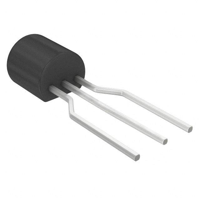
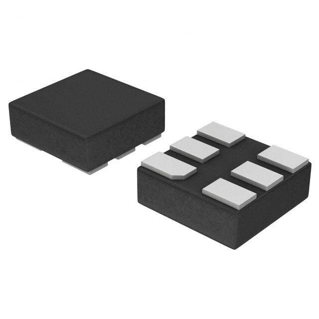
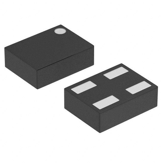
| 供应商器件封装 | 8-DFN(2x2) |
| 其它名称 | LTC2960IDC-3#TRMPBFCT |
| 包装 | 剪切带 (CT) |
| 受监控电压数 | 2 |
| 复位 | 低有效 |
| 复位超时 | 最小为 140 ms |
| 安装类型 | 表面贴装 |
| 封装/外壳 | 8-WFDFN 裸露焊盘 |
| 工作温度 | -40°C ~ 85°C |
| 标准包装 | 1 |
| 电压-阈值 | 可调节/可选择 |
| 类型 | 多压监控器 |
| 输出 | 推挽式,图腾柱 |


- 商务部:美国ITC正式对集成电路等产品启动337调查
- 曝三星4nm工艺存在良率问题 高通将骁龙8 Gen1或转产台积电
- 太阳诱电将投资9.5亿元在常州建新厂生产MLCC 预计2023年完工
- 英特尔发布欧洲新工厂建设计划 深化IDM 2.0 战略
- 台积电先进制程称霸业界 有大客户加持明年业绩稳了
- 达到5530亿美元!SIA预计今年全球半导体销售额将创下新高
- 英特尔拟将自动驾驶子公司Mobileye上市 估值或超500亿美元
- 三星加码芯片和SET,合并消费电子和移动部门,撤换高东真等 CEO
- 三星电子宣布重大人事变动 还合并消费电子和移动部门
- 海关总署:前11个月进口集成电路产品价值2.52万亿元 增长14.8%


PDF Datasheet 数据手册内容提取
LTC2960 36V Nano-Current Two-Input Voltage Monitor FeaTures DescripTion n 850nA Quiescent Current The LTC®2960 is a nano-current, high voltage two-input n Operating Range: 2.5V < VCC < 36V voltage monitor, ideally suited for multicell battery ap- n 1.5% (Max) Accuracy Over Temperature plications. External resistive dividers configure custom n Adjustable Reset Threshold comparator thresholds. The supervisory circuit monitors n Wide Temperature Range (–40°C to 125°C) the ADJ input and pulls the RST output low when the input n Adjustable IN+/IN– Threshold drops below threshold. A reset timeout period delays the n Manual Reset Input return of the RST output to a high state when the input n Compact 2mm × 2mm 8-lead DFN and rises above the threshold. The spare comparator allows TSOT-23 (ThinSOT™) Packages voltage conditions to be detected with either a non-inverting input, IN+(LTC2960-1/LTC2960-3) or an inverting input, applicaTions IN– (LTC2960-2/LTC2960-4). A manual reset (MR) input n Portable Equipment is provided for external activation of the reset output. n Battery Powered Equipment Other options provided on the LTC2960-1/LTC2960-2 in- n Security Systems clude a reset timeout period select pin, RT, to select between n Automotive Systems 15ms or 200ms reset timeout periods. The LTC2960-3/ LTC2960 Option Table LTC2960-4 have a fixed 200ms reset timeout period. The RST and OUT outputs are available with active pull-up cir- Option Inputs Reset Timeout Period Output Type LTC2960-1 ADJ/IN+ 15ms/200ms 36V Open-Drain cuits to an output logic supply pin (LTC2960-3/LTC2960-4) LTC2960-2 ADJ/IN– 15ms/200ms 36V Open-Drain or 36V open-drain outputs (LTC2960-1/LTC2960-2). LTC2960-3 ADJ/IN+ 200ms Active Pull-Up L, LT, LTC, LTM, Linear Technology and the Linear logo are registered trademarks and LTC2960-4 ADJ/IN– 200ms Active Pull-Up ThinSOT is a trademark of Linear Technology Corporation. All other trademarks are the property of their respective owners. Typical applicaTion Battery and Regulator Monitor Supply Current vs Supply Voltage 1200 6V < VIN < 8.4V VOUT MR=5V, 27C LTC3632 1.8V Li-Ion + R2 DC/DC R4 4.2V 6.04M GND 1.3M 900 C1 0.1µF LTC2960-3 C1µ2F A) 50V VCC DVCC (nC 600 IN+ RST RESET IC Li-Ion + R1 OUT LOW BATTERY 4.2V 402k MR ADJ 300 GND R3 402k 2960 TA01 0 0 8 16 24 32 40 POWER-FAIL FALLING THRESHOLD = 6.410V VCC (V) RESET FALLING THRESHOLD = 1.693V 2960 TA01a 2960fa 1 For more information www.linear.com/LTC2960
LTC2960 absoluTe MaxiMuM raTings (Notes 1 & 2) Input Voltages Average Currents V , RT, MR ..........................................–0.3V to 40V RST, OUT ...........................................................±5mA CC DV ........................................................–0.3V to 6V Operating Ambient Temperature Range CC ADJ, IN+, IN– .........................................–0.3V to 3.5V LTC2960C ................................................0°C to 70°C Output Voltages (LTC2960-1/LTC2960-2) LTC2960I .............................................–40°C to 85°C RST, OUT ...............................................–0.3V to 40V LTC2960H ..........................................–40°C to 125°C Output Voltages (LTC2960-3/LTC2960-4) Storage Temperature Range ..................–65°C to 150°C RST, OUT (DV ≥ 1.6V) .........–0.3V to (DV + 0.3V) Lead Temperature (Soldering, 10 sec) CC CC RST, OUT (DV = GND) .......................–0.3V to 6.3V TSOT-23 Package .............................................300°C CC pin conFiguraTion TOP VIEW VCC 1 8 IN+/IN– TOP VIEW RT/DVCC 2 7 ADJ IN+/IN– 1 8 VCC 9 RST 3 6 MR ADJ 2 7 RT/DVCC MR 3 6 RST OUT 4 5 GND GND 4 5 OUT DC8 PACKAGE TS8 PACKAGE 8-LEAD (2mm × 2mm) PLASTIC DFN 8-LEAD PLASTIC TSOT-23 TJMAX = 150°C, qJA = 80.6°C/W TJMAX = 150°C, qJA = 195°C/W EXPOSED PAD (PIN 9) PCB GND CONNECTION OPTIONAL orDer inForMaTion Lead Free Finish TAPE AND REEL (MINI) TAPE AND REEL PART MARKING PACKAGE DESCRIPTION TEMPERATURE RANGE LTC2960CDC-1#TRMPBF LTC2960CDC-1#TRPBF LFZZ 8-Lead (2mm × 2mm) Plastic DFN 0°C to 70°C LTC2960IDC-1#TRMPBF LTC2960IDC-1#TRPBF LFZZ 8-Lead (2mm × 2mm) Plastic DFN –40°C to 85°C LTC2960HDC-1#TRMPBF LTC2960HDC-1#TRPBF LFZZ 8-Lead (2mm × 2mm) Plastic DFN –40°C to 125°C LTC2960CDC-2#TRMPBF LTC2960CDC-2#TRPBF LGBC 8-Lead (2mm × 2mm) Plastic DFN 0°C to 70°C LTC2960IDC-2#TRMPBF LTC2960IDC-2#TRPBF LGBC 8-Lead (2mm × 2mm) Plastic DFN –40°C to 85°C LTC2960HDC-2#TRMPBF LTC2960HDC-2#TRPBF LGBC 8-Lead (2mm × 2mm) Plastic DFN –40°C to 125°C LTC2960CDC-3#TRMPBF LTC2960CDC-3#TRPBF LFSF 8-Lead (2mm × 2mm) Plastic DFN 0°C to 70°C LTC2960IDC-3#TRMPBF LTC2960IDC-3#TRPBF LFSF 8-Lead (2mm × 2mm) Plastic DFN –40°C to 85°C LTC2960HDC-3#TRMPBF LTC2960HDC-3#TRPBF LFSF 8-Lead (2mm × 2mm) Plastic DFN –40°C to 125°C LTC2960CDC-4#TRMPBF LTC2960CDC-4#TRPBF LGBF 8-Lead (2mm × 2mm) Plastic DFN 0°C to 70°C LTC2960IDC-4#TRMPBF LTC2960IDC-4#TRPBF LGBF 8-Lead (2mm × 2mm) Plastic DFN –40°C to 85°C LTC2960HDC-4#TRMPBF LTC2960HDC-4#TRPBF LGBF 8-Lead (2mm × 2mm) Plastic DFN –40°C to 125°C 2960fa 2 For more information www.linear.com/LTC2960
LTC2960 orDer inForMaTion Lead Free Finish TAPE AND REEL (MINI) TAPE AND REEL PART MARKING PACKAGE DESCRIPTION TEMPERATURE RANGE LTC2960CTS8-1#TRMPBF LTC2960CTS8-1#TRPBF LTFZY 8-Lead Plastic TSOT-23 0°C to 70°C LTC2960ITS8-1#TRMPBF LTC2960ITS8-1#TRPBF LTFZY 8-Lead Plastic TSOT-23 –40°C to 85°C LTC2960HTS8-1#TRMPBF LTC2960HTS8-1#TRPBF LTFZY 8-Lead Plastic TSOT-23 –40°C to 125°C LTC2960CTS8-2#TRMPBF LTC2960CTS8-2#TRPBF LTGBB 8-Lead Plastic TSOT-23 0°C to 70°C LTC2960ITS8-2#TRMPBF LTC2960ITS8-2#TRPBF LTGBB 8-Lead Plastic TSOT-23 –40°C to 85°C LTC2960HTS8-2#TRMPBF LTC2960HTS8-2#TRPBF LTGBB 8-Lead Plastic TSOT-23 –40°C to 125°C LTC2960CTS8-3#TRMPBF LTC2960CTS8-3#TRPBF LTFSD 8-Lead Plastic TSOT-23 0°C to 70°C LTC2960ITS8-3#TRMPBF LTC2960ITS8-3#TRPBF LTFSD 8-Lead Plastic TSOT-23 –40°C to 85°C LTC2960HTS8-3#TRMPBF LTC2960HTS8-3#TRPBF LTFSD 8-Lead Plastic TSOT-23 –40°C to 125°C LTC2960CTS8-4#TRMPBF LTC2960CTS8-4#TRPBF LTGBD 8-Lead Plastic TSOT-23 0°C to 70°C LTC2960ITS8-4#TRMPBF LTC2960ITS8-4#TRPBF LTGBD 8-Lead Plastic TSOT-23 –40°C to 85°C LTC2960HTS8-4#TRMPBF LTC2960HTS8-4#TRPBF LTGBD 8-Lead Plastic TSOT-23 –40°C to 125°C Consult LTC Marketing for parts specified with wider operating temperature ranges. Consult LTC Marketing for information on nonstandard lead based finish parts. For more information on lead free part marking, go to: http://www.linear.com/leadfree/ For more information on tape and reel specifications, go to: http://www.linear.com/tapeandreel/ elecTrical characTerisTics The l denotes specifications that apply over the full operating temperature range, otherwise specifications are at T = 25°C, V = 7V, DV = 3.3V unless otherwise noted (Note 2). A CC CC SYMBOL PARAMETER CONDITIONS MIN TYP MAX UNITS V V Input Supply Operating Range l 2.5 36 V CC CC V V Undervoltage Lockout V Rising l 1.85 2.3 V UVLO CC CC V Undervoltage Lockout Hysteresis 100 mV CC I V Input Supply Current MR = 5V, V = 36V, –40°C ≤ T ≤ 85°C l 400 850 1250 nA CC CC CC A MR = 5V, V = 36V, –40°C ≤ T ≤ 125°C l 400 850 2000 nA CC A DV DV Input Supply Operating Range l 1.6 5.5 V CC CC I DV Input Current RST = OUT = LOW DV = 5.5V l ±50 nA DVCC CC CC THRESHOLD ADJUSTMENT INPUTS: ADJ, IN+/IN– VTH ADJ/IN+ Input Threshold Monitored Voltage Falling l 394 400 406 mV IN– Input Threshold Monitored Voltage Rising l 394 400 406 mV V ADJ to IN+/IN– Threshold Matching l ±2 ±6 mV THM V ADJ Threshold Hysteresis Monitored Voltage Rising l 8 10 15 mV RHYS V+ IN+ Threshold Hysteresis Monitored Voltage Rising l 18 20 25 mV HYS V– IN– Threshold Hysteresis Monitored Voltage Falling l 18 20 25 mV HYS t Under Voltage Detect to RST, OUT Falling V = V – 40mV l 80 170 500 µs UV TH I Input Leakage Current V = 420mV, –40°C ≤ T ≤ 85°C l ±0.1 ±1 nA TH(LKG) A V = 420mV, –40°C ≤ T ≤ 125°C l ±0.1 ±10 nA A 2960fa 3 For more information www.linear.com/LTC2960
LTC2960 elecTrical characTerisTics The l denotes specifications that apply over the full operating temperature range, otherwise specifications are at T = 25°C, V = 7V, DV = 3.3V unless otherwise noted (Note 2). A CC CC SYMBOL PARAMETER CONDITIONS MIN TYP MAX UNITS CONTROL INPUTS: MR, RT V Control Input Threshold RT l 0.4 1.4 V RT V Control Input Threshold MR l 0.4 1.4 V MR t MR Minimum Detectable Pulse Width l 20 µs PW t Propagation Delay to RST Falling Manual Reset Falling l 1 7 20 µs PD V Manual Reset Open Voltage MR Open, MR Load = 100nA l 2.6 4 V MR I Manual Reset Low Current MR = 400mV, V ≥ 2.5V l –0.35 –1 –3 µA MR CC I Input Leakage Current RT = 15V l ±100 nA LK MR = 15V l ±100 nA STATUS OUTPUTS: RST, OUT V Voltage Output Low V = 1.2V, I = 10µA (LTC2960-1/LTC2960-3) l 25 100 mV OL CC V = 3V, I = 500µA l 100 400 mV CC V Voltage Output High I = –100µA (LTC2960-3/LTC2960-4) l 0.7•DV V OH CC I Leakage Current, Output High V = 5.5V l ±50 nA OH V = 15V (LTC2960-1/LTC2960-2) l ±100 nA V = 5.5V, DV = GND l ±50 nA CC I Output Short-Circuit Current RST = GND DV = 6V (LTC2960-3/ LTC2960-4) l 0.8 3 mA SC CC OUT = GND DV = 6V (LTC2960-3/ LTC2960-4) l 0.8 3 mA CC t Reset Timeout Period LTC2960-3/LTC2960-4 l 140 200 280 ms RST RT Input High l 140 200 280 ms RT Input Low l 10 15 25 ms Note 1: Stresses beyond those listed under Absolute Maximum Ratings Note 2. All currents into pins are positive; all voltages are referenced to may cause permanent damage to the device. Exposure to any Absolute GND unless otherwise noted. Maximum Rating condition for extended periods may affect device reliability and lifetime. Typical perForMance characTerisTics Supply Current vs Supply Voltage MR Current vs MR Voltage Supply Current vs MR Voltage 1500 1.2 2.5 VCC = 7V 1200 125°C 1.0 2.0 VCC = 7V VCC = 2.5V 90°C A) 0.8 A) A) 900 NT (µ NT (µ 1.5 I (nCC 600 27°C CURRE 0.6 CURRE 1.0 –45°C MR 0.4 MR VCC = 2.5V 300 0.5 0.2 0 0 0 0 8 16 24 32 40 0 1 2 3 4 5 0 1 2 3 4 5 VCC(V) MR VOLTAGE (V) MR VOLTAGE (V) 2960 G01 2960 G02 2960 G03 2960fa 4 For more information www.linear.com/LTC2960
LTC2960 Typical perForMance characTerisTics MR Rising Threshold/Open Normalized Reset Timeout Period Comparator Overvoltage/ Voltage vs V vs Temperature Undervoltage Glitch Immunity CC 1.3 4.0 AGE (V) 2.4 RIOD 1.2 VCC = 7V ADJV/CINC +=/I 7NV– SING THRESHOLD/OPEN VOLT 110...949 MMRR O INPEPNU TV OTHLTRAEGSEH 2O7L°DC 27°C NORMALIZED RESET TIME PE 1010....1908 GLITCH DURATION (ms) 312...000 RI 0.4 0.7 0.0 2.5 3.0 3.5 4.0 4.5 5.0 –50 –25 0 25 50 75 100 125 0.1 1 10 100 VCC (V) TEMPERATURE (°C) COMPARATOR OVERDRIVE (%) 2960 G04 2960 G05 2960 G06 ADJ, IN+, IN– Threshold Voltage Output HIGH vs vs Temperature Pull-Down Current (RST/OUT) 430 3.5 125°C V+HYS 3.0 90°C 420 27°C –45°C VRHYS 2.5 410 (mV)H 400 VTH (V)OH 2.0 VT V 1.5 390 1.0 V–HYS 380 0.5 VCC =7V DVCC =3.3V 370 0 –50 –25 0 25 50 75 100 125 0 –0.2 –0.4 –0.6 –0.8 TEMPERATURE (°C) PULL-DOWN CURRENT(mA) 2960 G07 2960 G08 Voltage Output LOW vs Voltage Output HIGH vs Pull-Up Current (RST/OUT) Pull-Down Current (RST/OUT) 2.0 2.0 125°C 125°C 90°C 90°C 27°C 27°C 1.6 1.6 –45°C –45°C 1.2 1.2 V) V) (OL (OH V V 0.8 0.8 0.4 0.4 VCC =7V VCC =7V DVCC =3.3V DVCC =1.6V 0 0 0 1 2 3 4 5 0 –20 –40 –60 –80 PULL-UP CURRENT (mA) PULL-DOWN CURRENT(µA) 2960 G09 2960 G08 2960fa 5 For more information www.linear.com/LTC2960
LTC2960 pin FuncTions ADJ: Reset Threshold Adjustment Input. Tie to resistive OUT: (LTC2960-1/LTC2960-3) Pulls low when monitored divider to configure desired reset threshold. voltage falls below the IN+ threshold. Released when the IN+ voltage rises above its threshold by 5%. For the DV : (LTC2960-3/LTC2960-4) Logic Supply Input. Used CC LTC2960-3, OUT is driven by DV when logic high. OUT for setting the logic swing of the RST and OUT outputs. CC is open drain if DV is grounded. Leave open if unused. Useful for interfacing with logic voltages different from CC (LTC2960-2/LTC2960-4) OUT pulls low when the moni- V . Bypass DV with 0.1µF to GND. Grounding DV CC CC CC tored voltage rises above the IN– threshold. Released when allows OUT and RST to act as open drain outputs. monitored voltage falls below IN– threshold by 5%. For the Exposed Pad (DFN Only): Exposed pad may be left floating LTC2960-4, OUT is driven to DV for a logic high. OUT CC or connected to device ground. is open drain if DV is grounded. Leave open if unused. CC GND: Device ground. RST: Reset Output. Pulls low when monitored voltage falls IN–: (LTC2960-2/LTC2960-4) IN– Threshold Adjustment below the reset (ADJ) threshold. RST is released after monitored voltage exceeds the reset threshold plus 2.5% Input. Tie to resistive divider to configure required thresh- hysteresis and after reset timeout period has expired. For old. Tie to GND if unused. the LTC2960-3/LTC2960-4, RST is driven to DV for a CC IN+: (LTC2960-1/LTC2960-3) IN+ Threshold Adjustment logic high. RST is open drain if DV is grounded. Leave CC Input. Tie to resistive divider to configure required thresh- open if unused. old. Tie to GND if unused. RT: (LTC2960-1/LTC2960-2) Reset Timeout Period Se- MR: Manual Reset Input. Attach a push-button switch or lection Input. Tie to GND for 15ms delay. Tie to V for CC logic signal between this input and ground. A logic low on 200ms delay. this input pulls RST low. When the MR input returns to V : Power Supply Input. When V falls below the falling logic high, RST returns high after a reset timeout period CC CC UVLO threshold, the outputs are pulled low. If V falls has expired. Leave open if unused. CC below 1.2V the logic state of the outputs cannot be guar- anteed. Bypass V with 0.1µF to GND. Use appropriate CC voltage rating for bypass capacitor. 2960fa 6 For more information www.linear.com/LTC2960
LTC2960 block DiagraM RT DVCC VCC 400mV LTC2960-1/LTC2960-2 LTC2960-3/LTC2960-4 REGULATOR 0.4V REFERENCE 1µA MR RST ADJ – RESET DELAY + 0.4V LTC2960-2/LTC2960-4 OUT + IN+ (LTC2960-1/LTC2960-3) IN– (LTC2960-2/LTC2960-4) – LTC2960-1/LTC2960-3 GND 2960 BD TiMing DiagraM IN+/OUT TIMING VTH + V+HYS VTH VIN+ OUT IN–/OUT TIMING VTH VTH + V–HYS VIN– OUT ADJ/RST TIMING VTH + VRHYS VTH VADJ tRST tRST RST MR 2960 TD tPD 2960fa 7 For more information www.linear.com/LTC2960
LTC2960 applicaTions inForMaTion VOLTAGE MONITORING THRESHOLD CONFIGURATION The LTC2960 is a voltage supervisor with a wide operating The LTC2960 monitors voltage applied to its inputs IN+/IN– voltage range up to 36V with only 850nA quiescent current. and ADJ. A resistive divider connected between a monitored The supervisor has two outputs, RST and OUT that pro- voltage and ground is used to bias the inputs. Figure 1 vide voltage monitoring capabilities for system power-up, demonstrates how the inputs can be made dependent upon power-down and brown-out conditions. Built-in hysteresis a single voltage (V1). Only three resistors are required. and a reset timeout period ensure that fluctuations due to To calculate their values, specify desired falling reset (V ) R load transients or supply noise do not cause chattering of and IN+ (VIN+) thresholds with VIN+ > VR. For example: the status outputs. The LTC2960 can provide reset and VIN+ = 6.4V, VR = 6V voltage status signals to a microprocessor based system or can alternatively be used as an Under Voltage Lock Out V1 (UVLO) for DC/DC switchers or LDOs for control over a LTC2960-1/ R3 LTC2960-3 battery operated system. ADJ RST If the monitored voltage drops below the reset threshold, RST pulls low until the ADJ input rises above 0.4V plus R2 2.5% hysteresis. An internal reset timer delays the return IN+ OUT of the RST output to a high state to provide monitored 2960 F01 voltage settling and initialization time. The RST output is R1 typically connected to a processor reset input. If the monitored supply voltage falls to the IN+ (LTC2960-1/ Figure 1. Configuration for Single Voltage Monitoring LTC2960-3) threshold, the spare comparator pulls OUT low. OUT remains low until the IN+ input rises above 0.4V plus The solution for R1, R2 and R3 provides three equations 5% hysteresis. OUT is typically used to signal preparation and three unknowns. Maximum resistor size is governed for controlled shutdown. For example, the OUT output by maximum input leakage current. For the LTC2960, the may be connected to a processor nonmaskable interrupt maximum input leakage current below 85°C is 1nA. For (NMI). Upon interrupt, the processor begins shutdown a maximum error of 1% due to both input currents, the procedures such as supply sequencing and/or storage/ resistor divider current should be at least 100 times the erasure of system state in nonvolatile memory. sum of the leakage currents, or 0.2µA. If the total divider If the monitored supply voltage rises to the IN– threshold resistance is chosen arbitrarily to be 8MΩ, such as in this (LTC2960-2/LTC2960-4), the spare comparator pulls OUT example, then the current is 750nA at the reset threshold. low. OUT remains low until the IN– falls below 0.4V minus This results in a leakage current error well below 1%. 5% hysteresis. The LTC2960-2/LTC2960-4 operates as an For R = 8MΩ, then: SUM undervoltage and overvoltage monitor. R = R1 + R2 + R3 SUM Few, if any, external components are necessary for reliable Both the falling reset and IN+ thresholds are 0.4V, so: operation. However, a decoupling capacitor between V CC and ground is recommended (0.01µF minimum). Use a R1= VTH•RSUM = 0.4V•8MΩ =500k capacitor with a compatible voltage rating. VIN+ 6.4V The closest 1% value is 499k. R2 can be determined from: V •R 0.4V•8MΩ R2= TH SUM –R1= –499k V 6V R R2 = 34.33k 2960fa 8 For more information www.linear.com/LTC2960
LTC2960 applicaTions inForMaTion The closest 1% resistor value is 34k. R3 is easily obtained to a user defined voltage up to 36V with a resistor. The from: open-drain pull-up voltage may be greater than V . Select CC a resistor compatible with desired output rise time and R3 = R – R1 – R2 = 8M – 499k – 34k SUM load current specifications. Figure 3 demonstrates typical R3 = 7.467MΩ LTC2960-1 OUT output behavior. When the status outputs are low, power is dissipated in the pull-up resistors. The closest 1% resistor value is 7.5MΩ. Plugging the standard values back into the equations yields the design 7.5 values for the falling reset and IN+ voltages: VIN+ = 6.4V, VRST = 6.028V 6 Figure 2 demonstrates how the inputs can be biased 4.5 to monitor two voltages (V1, V2). In this example, four T (V) U resistors are required. Calculate each divider ratio for the O 3 desired falling threshold (V ) using: FT RnB VFT VFT 1.5 = –1= –1 RnA V 0.4V TH 0 0 1.5 3 4.5 6 7.5 In Figure 2, OUT is tied back to the MR input, making the VCC (V) state of the RST output dependent upon both V1 and V2. If 2960 F03 V1 and V2 are both above the configured falling threshold Figure 3. OUT vs V (LTC2960-1) Externally Configured for CC plus hysteresis, RST is allowed to pull high. If independent 6V Threshold with RST Tied to V Through Pull-Up Resistor CC operation of the status outputs is desired, simply omit the OUT and MR connection. The outputs of both the LTC2960-3 and LTC2960-4 can be configured as either low voltage active pull-up or open- V1 V2 drain. This is done by tying the DVCC pin to either a supply or GND. Using the active pull-up configuration, DV tied LTC2960-1/ CC R2B R1B LTC2960-3 to a supply, lowers power dissipation by eliminating the static current drawn by pull-up resistors when the outputs ADJ RST are low and improves output rise time. In Figure 4(a), an LTC2960-3 has active pull-up outputs configured by tying IN+ OUT DVCC to a 1.6V to 5.5V supply. In Figure 4(b), the LTC2960-3 MR has open-drain outputs configured by tying the DV pin to 2960 F02 CC R2A R1A ground. When DV is connected to ground both outputs CC are open-drain and pull-up resistors are required. Some applications require RST and/or OUT outputs to Figure 2. Dual Voltage Monitoring be valid with V down to ground when DV is tied to CC CC V . Active pull-up satisfies this requirement with the ad- CC dition of an optional external resistor from the output to SELECTING OUTPUT LOGIC STYLE ground. The resistor provides a path for leakage currents, The LTC2960 status outputs are available in two options: preventing the output from floating to undetermined volt- open-drain (LTC2960-1/LTC2960-2) or active pull-up with ages when connected to high impedance (such as CMOS the DV pin replacing the RT pin (LTC2960-3/LTC2960-4). logic inputs). The resistor value should be small enough to CC The open-drain option allows the outputs to be pulled up provide effective pull-down without excessively loading the 2960fa 9 For more information www.linear.com/LTC2960
LTC2960 applicaTions inForMaTion pull-up circuitry. A 100k resistor from output to ground is and MR is a solution to this issue. The MR input can be satisfactory for most applications. When the status outputs pulled to 36V maximum and will not affect the internal are high, power is dissipated in the pull-down resistors. circuitry. Input MR is often pulled down through the use of a pushbutton switch. If V falls below the falling UVLO threshold, the outputs CC are pulled to ground. The outputs are guaranteed to stay low for V ≥ 1.2V regardless of the output logic configura- SELECTING THE RESET TIMEOUT PERIOD CC tion. When V < 1.2V, the active pull-up output behaves CC Use the RT input (LTC2960-1/ LTC2960-2) to select similarly to an open-drain output with a pull-up resistor. between two fixed reset timeout periods. Connect RT to ground for a 15ms timeout. Connect RT to V for a 200ms CC timeout. The reset timeout period occurs after the ADJ LTC2960-3 input is driven above threshold and the MR input transitions DVCC 1.6V TO 5.5V above its logic threshold. After the reset timeout period, the RST output is allowed to pull up to a high state as shown in Figure 5. The RT input is replaced by the DV CC 0.4V OUT + input in the LTC2960-3/LTC2960-4 options and the reset timeout period defaults to 200ms. IN+ – ADJ (a). PUSH-PULL CONFIGURATION 15ms LTC2960-3 RST, RT = GND DVCC 200ms 6.3V MAX RST, RT = VCC 2960 F05 0.4V + OUT Figure 5. Selectable Reset Timeout Period IN+ – EXTERNAL HYSTERESIS The LTC2960 IN+ comparator hysteresis is 20mV (V+ ), (b). OPEN-DRAIN CONFIGURATION 2960 F04 HYS or 5% referred to V . Certain applications require more TH Figure 4. LTC2960-3 (LTC2960-4) RST and OUT Outputs than the built-in native hysteresis. The application sche- Are Configurable as Push-Pull or Open-Drain matic in Figure 6 adds one additional resistor (R6) to a typical attenuator network. The procedure below is used MANUAL RESET INPUT to determine a value for R6 to provide an increase over the native hysteresis. In this example, it is desired to double When ADJ is above its reset threshold and the manual the native hysteresis from 300mV to 600mV and achieve reset input (MR) is pulled low, the RST output is forced a falling threshold of 6V. low. RST remains low for the selected reset timeout period after the manual reset input is released and pulled high. Before including R6, the rising threshold (V ) is 6.293V R The manual reset input is pulled up internally through a while the falling threshold (V ) is 5.993V. The hysteresis F 1µA current source to an internal bias voltage (see Elec- referred to V is calculated from: A trical Characteristics). If external leakage currents have R4 the ability to pull down the manual reset input below its VHYST(VA) =VPHYS1+R5=20mV•15=300mV logic threshold, a pull-up resistor placed between V CC 2960fa 10 For more information www.linear.com/LTC2960
LTC2960 applicaTions inForMaTion The falling threshold can be restored to the original value VA VB by reducing the value of R5. Under the assumption that LTC2960-3 the addition of R6 has a negligible impact on the rising R4 681k DVCC threshold, a new R4/R5 ratio can be calculated as shown: R4 V 6.6V = R –1= –1=14.71 IN+ OUT R5 (VTH+V+HYS) 420mV R5 R6 Given the ratio of R4/R5, the closest 1% resistor value for 48.7k 6.81M R5 is 46.4k. With the actual resistor values now known, 2960 F06 the final thresholds can be calculated by plugging the values into the equations above for V and V to obtain: R F Figure 6. External Hysteresis V =6.626V,V =6.010V,V =616mV R F HYST The addition of R6 allows OUT to sink or source current to the summing junction at IN+. Neglecting internal switch As a result of the added current component through R6 resistances and providing that R6 >> R5, the externally an error term exists that is a function of the pull-up volt- modified hysteresis (referred to VA) becomes: age, VB in Figure 6. R4 VHEXT ≈ VHYS(VA) +VBR6 Operation with Supply Transients over 40V and Hot Swapping Since the amount of hysteresis is to be doubled, the The circuit in Figure 7(a) allows the LTC2960 to withstand second term in the above expression needs to be about high voltage transients. The magnitude of the voltage 300mV. With a logic supply, V , equal to 3V, the ratio R4/ B transients that can be absorbed is set by the voltage rat- R6 should be about 0.1. Choosing R6 to be 6.81M satisfies ing of RZ. A TT-IRC pulse-withstanding surface mount the design criteria. 1206 resistor with a nominal voltage rating of 200V is The addition of R6 modifies the rising and falling thresholds used. The external 30V Zener diode (Z1) and the 143kΩ originally determined by R4 and R5. The modified rising current limiting resistor (RZ) protect the VIN supply pin threshold becomes: of the LTC2960. Note that there is a speed penalty which is the time constant determined by RZ and C1, 14.3ms in R4 R4 VR=(VTH+V+HYS)•1+ + this example. If VIN is below 30V, there is a voltage drop R5 R6 across RZ that is dependent on the quiescent current of the LTC2960 which is nominally less than 150mV but can =(400mV+20mV)•(1+13.98+0.1) be as high as 290mV if MR is pulled low. The maximum voltage drop is determined by the maximum specified I =6.3336V CC and MR pull-up currents. For conditions where the Zener conducts current, it can be biased in the microamp range It is apparent that the R4/R6 term does not affect the ris- owing to the low quiescent current of the LTC2960. For a ing threshold significantly resulting in a change of only supply voltage of 150V, the Zener is biased <1mA. When +0.645%. The falling threshold incorporating R6 is: input pins are used to sense V , the input pins ADJ/IN+/ IN R4 R4 V –V IN– absolute maximum rating of 3.5V must not be exceeded. TH B VF = VTH1+ R5 +R6 VTH VIN can be a maximum of 8.75x the lowest programmed threshold to satisfy this condition. For a maximum V of IN =0.4V•(1+13.98–0.65)=5.732V 150V, the lowest programmable threshold is >17V. 2960fa 11 For more information www.linear.com/LTC2960
LTC2960 applicaTions inForMaTion When a supply voltage is abruptly connected to the input VIN MAX 200V resonant ringing can occur as a result of series inductance. RZ The peak voltage could rise to 2x the input supply but in 143k PWC1206LF143kJ* practice can reach 2.5x if a capacitor with a strong volt- VCC age coefficient is present. If a 12V supply is hot plugged Z1 C1 LTC2960 BZX84C30 0.1µF the resulting ringing could reach the abs max of V . Any BV = 30V 50V CC circuit with an input of more than 7V should be scrutinized *TT-IRC for ringing. Circuit board trace inductances of as little as (a) 10nH can produce significant ringing. VIN One effective means to eliminate ringing is to include a RS 20 10–100Ω resistance in series with the supply input before VCC the V capacitor shown in Figure 7(b). This provides damp- CC C1 LTC2960 ing for the resonant circuit but imposes a time constant to 0.1µF 50V V . In Figure 7(b), the time constant of RS and C1 is 2µs. CC 2960 F07 (b) Figure 7. Operation with High Voltage Transients and Hot Swapping 2960fa 12 For more information www.linear.com/LTC2960
LTC2960 Typical applicaTions Configurable Regulator UVLO and Low Battery internal switch when it reaches 2.5V. With a threshold of Indicator 5.537V the LTC2960 OUT output disables the load before this occurs in order to prevent damage to the batteries. In the circuit of Figure 8, the high voltage open drain In addition to the UVLO signal, the LTC2960 provides a OUT output is used as a configurable UVLO signal for a low battery indicator for the system. Figure 9 shows an switching regulator. A Li-Ion battery can contain protec- alternative arrangement in which the LTC2960 monitors tion circuitry that open circuits its terminals through an the output of the 3.3V regulator to provide a reset signal. BUCK CONVERTER VBAT NOT ALL LT3991 COMPONENTS SHOWN 6V TO 8.4V VOUT VIN VOUT 3.3V R3 R4 5.11M* 10M LT3991 C2 Li-Ion + EN 47µF R1M5 4.2V C1 VCC GND 16V 0.1µF RT OUT 25V IN+ R2 LTC2960-1 + 49.9k Li-Ion ADJ RST LOW BATTERY 4.2V R1 MR 348k GND 2960 F08 UVLO FALLING THRESHOLD = 5.537V *VISHAY-DALE CRCW SERIES 0603 1% RESET FALLING THRESHOLD = 6.33V Figure 8. Configurable Regulator UVLO and Low Battery Indicator BUCK CONVERTER VBAT NOT ALL LT3991 COMPONENTS SHOWN 6V TO 8.4V VOUT VIN VOUT 3.3V R5 Li-Ion + R6.204M 10M LT3991 C2 R4 R6 4.2V C1 VCC EN 47µF 2.26M 1M 0.1µF RT OUT GND 16V 25V LTC2960-1 Li-Ion + IN+ ADJ 4.2V MR RST RESET R1 RESD* GND R3 402k 10k 2960 F09 402k UVLO FALLING THRESHOLD = 6.410V *OPTIONAL RESISTOR FOR ADDED ESD PROTECTION RESET FALLING THRESHOLD = 2.649V Figure 9. Configurable Regulator UVLO and Supervisor 2960fa 13 For more information www.linear.com/LTC2960
LTC2960 Typical applicaTions The LTC2960-2 in Figure 10 is yet another way to prevent current in the event of a reverse battery condition. In all excessive discharge of a battery. The high voltage OUT three examples, the load drops to <2.5µA typically and output is used to drive the gate of a PMOS switch to in- excessive battery drain is prevented. terrupt the path to V in the event of an undervoltage OUT Automotive Supervisor (LTC2960 H-Grade) condition. When the battery stack voltage is above the IN– rising threshold of 5.972V, the PMOS switch is turned The circuit in Figure 11 uses the LTC2960-3 (H-grade) as a on. The LTC2960-2 also supervises V to provide a low low voltage supervisor capable of operating in temperatures OUT battery signal as an early warning of impending shutdown. up to 125°C in automotive environments. The LT4356 A 10k resistor is included in series with the V pin to limit surge stopper limits V to 27V under the alternator load CC IN VBAT M2 M1 6V TO 8.4V Si4435 Si4435 VOUT R8 1N5245 R7 10k 15V 1M + Li-Ion R2 R6 R4 R5 4.2V C1 5.6M* VCC 100k 6.04M* 10M 0.1µF RT OUT 25V ADJ LTC2960-2 + Li-Ion IN– RST LOW BATTERY 4.2V R1 R3 MR 402k* 402k* GND IN– FALLING THRESHOLD = 5.974V 2960 F10 ADJ FALLING THRESHOLD = 6.410V *VISHAY-DALE CRCW SERIES 0603 1 % Figure 10. Battery Disconnect to Protect Against Deep Discharge BUCK CONVERTER VIN NOT ALL LT3991 COMPONENTS SHOWN VEHICLE BATTE1R2VY IRLR2908 4V TO 27V VIN VOUT 3V.O3UVT R8 R2 R7 LT3991 R4 R6 102k 825k 1M 1.78M 6.04M C2 EN/SS FB VCC GATE OUT GND R3 22µF FB C1 1M VCC DVCC 25V LT4356 1µF IN+ ADJ 50V LTC2960-3 FLT GND OUT RST UV R7 R1 MR R5 4.99k 80.6k GND 1M OV 2960 F11 IN+ FALLING THRESHOLD = 4.49V ADJ FALLING THRESHOLD = 2.816V Figure 11. Automotive Supervisor 2960fa 14 For more information www.linear.com/LTC2960
LTC2960 Typical applicaTions dump condition. The LT3991 buck regulator in conjunc- Micropower Power Supply Sequencer and Supervisor tion with the LTC2960 draw <10µA quiescent current for Figure 13 illustrates multiple uses for the LTC2960 in a no load, which limits the drain on the vehicle battery even power supply system. U1 is a power supply sequencer after long periods of inactivity. whose IN+ input monitors V and enables the 5V switch- IN ing regulator. The ADJ input monitors the output of the Window Comparator for High Voltage Input 5V switching regulator and enables the 1.8V LDO after a The LTC2960-4 can be configured as a window compara- 16ms Reset Timeout Period. U2 is a supervisor monitor- tor to monitor high voltage supplies or battery stacks as ing the 5V and 1.8V outputs. The OUT output by virtue shown in Figure 12. A fault signal is generated if VIN is out of the MR pin, keeps the RST output low until the 1.8V of regulation. The OUT output of the LTC2960-4 is fed back supply is ready. into the MR input to drive the RST output. A micropower LDO provides bias to the active pull-up DV supply for CC low static current draw in the outputs. 16V.4IVN VIN OUT 5VVOUT R3B R4 LT3009-5 C2 20mA MAX 118k* 10k 1µF SHDN 16V R3A GND 7.32M* C1 VCC 0.1µF DVCC 50V ADJ R2 LTC2960-4 68k* IN– RST FAULT OUT R1 GND MR 182k* 2960 F12 UPPER THRESHOLD = 16.897V *VISHAY-DALE CRCW SERIES 0603 1% LOWER THRESHOLD = 12.3V Figure 12. Window Comparator for High Voltage Input 2960fa 15 For more information www.linear.com/LTC2960
LTC2960 package DescripTion Please refer to http://www.linear.com/designtools/packaging/ for the most recent package drawings. DC8 Package 8-Lead Plastic DFN (2mm × 2mm) (Reference LTC DWG # 05-08-1719 Rev A) R = 0.115 TYP R = 0.05 5 8 0.70 ±0.05 TYP 0.40 ±0.10 2.55 ±0.05 1.15 ±0.050.64 ±0.05 2.00 ±0.10 0.64 ±0.10 PIN 1 NOTCH (2 SIDES) POAUCTKLIANGEE (SETPEOI NPN OM1T BAEAR 6RK) (4 SIDES) (2 SIDES) R0C.H 2=A5 0M ×.2F 40E5 RO° R (DC8) DFN 0409 REVA 4 1 0.25 ±0.05 0.23 ±0.05 0.45 BSC 0.200 REF 0.75 ±0.05 0.45 BSC 1.37 ±0.05 1.37 ±0.10 (2 SIDES) (2 SIDES) RECOMMENDED SOLDER PAD PITCH AND DIMENSIONS 0.00 – 0.05 BOTTOM VIEW—EXPOSED PAD APPLY SOLDER MASK TO AREAS THAT ARE NOT SOLDERED NOTE: 4. DIMENSIONS OF EXPOSED PAD ON BOTTOM OF PACKAGE DO NOT INCLUDE 1. DRAWING IS NOT A JEDEC PACKAGE OUTLINE MOLD FLASH. MOLD FLASH, IF PRESENT, SHALL NOT EXCEED 0.15mm ON ANY SIDE 2. DRAWING NOT TO SCALE 5. EXPOSED PAD SHALL BE SOLDER PLATED 3. ALL DIMENSIONS ARE IN MILLIMETERS 6. SHADED AREA IS ONLY A REFERENCE FOR PIN 1 LOCATION ON THE TOP AND BOTTOM OF PACKAGE TS8 Package 8-Lead Plastic TSOT-23 (Reference LTC DWG # 05-08-1637 Rev A) 2.90 BSC 0.40 0.65 (NOTE 4) MAX REF 1.22 REF 1.50 – 1.75 3.85 MAX2.62 REF 1.4 MIN 2.80 BSC (NOTE 4) PIN ONE ID RECOMMENDED SOLDER PAD LAYOUT 0.22 – 0.36 0.65 BSC PER IPC CALCULATOR 8 PLCS (NOTE 3) 0.80 – 0.90 0.20 BSC 0.01 – 0.10 1.00 MAX DATUM ‘A’ 0.30 – 0.50 REF 1.95 BSC 0.09 – 0.20 TS8 TSOT-23 0710 REV A (NOTE 3) NOTE: 1. DIMENSIONS ARE IN MILLIMETERS 4. DIMENSIONS ARE EXCLUSIVE OF MOLD FLASH AND METAL BURR 2. DRAWING NOT TO SCALE 5. MOLD FLASH SHALL NOT EXCEED 0.254mm 3. DIMENSIONS ARE INCLUSIVE OF PLATING 6. JEDEC PACKAGE REFERENCE IS MO-193 2960fa 16 For more information www.linear.com/LTC2960
LTC2960 revision hisTory REV DATE DESCRIPTION PAGE NUMBER A 12/13 Inverted OUT waveform in IN–/OUT Timing Diagram 7 2960fa Information furnished by Linear Technology Corporation is believed to be accurate and reliable. 17 However, no responsibility is assumed for its use. Linear Technology Corporation makes no representa- tion that the interconneFcotior nm oof irtse ciinrcfouirtms aast dioensc wribwedw h.leinreeina rw.cilol nmot/ LinTfCrin2g9e6 o0n existing patent rights.
LTC2960 Typical applicaTion BUCK CONVERTER NOT ALL LT3991 COMPONENTS SHOWN 5V 6.6V < VIN < 36V VIN VOUT OUTPUT R2 R3 LT3991 C2 6.04M 10M 47µF EN 16V LTC2960-1 GND R5 3.48M 1.8V C1 VCC OUT IN OUT OUTPUT 0.1µF ADJ R6 LT3009-1.8 C3 25V IN+ 15ms DELAY 1M SHDN 1µF U1RST GND R8 10V R1 MR RT R4 1.3M 402k 402k GND R9 LTC2960-1 1M VCC RT ADJ VIN SUPPLY UVLO = 6.410V U2 IN+ 200ms DELAY 1.8V SUPPLY UVLO = 3.863V OUT RST RST RESET THRESHOLD = 1.693V MR GND R7 402k 2960 F14 Figure 13. Micropower Power Supply Sequencer and Supervisor relaTeD parTs PART NUMBER DESCRIPTION COMMENTS LTC1326 Micropower Triple-Supply Monitor for 5V/2.5V, 3.3V and ADJ 4.725V, 3.118V, 1V Threshold (±0.75%) and ADJ LTC1726 Micropower Triple-Supply Monitor for 2.5V/5V, 3.3V and ADJ Adjustable Reset and Watchdog Timeouts LTC1727 Micropower Triple-Supply Monitor with Open-Drain Reset Individual Monitor Outputs in MSOP LTC1728 Micropower Triple-Supply Monitor with Open-Drain Reset 5-Lead SOT-23 Package LTC1985 Micropower Triple-Supply Monitor with Push-Pull Reset Output 5-Lead SOT-23 Package LTC2900/LTC2901/ Programmable Quad-Supply Monitor Adjustable Reset, Watchdog Timer and Tolerance, 10-Lead LTC2902 MSOP and DFN Packages LTC2903 Precision Quad-Supply Monitor 6-Lead SOT-23 and DFN Packages LTC2904/LTC2905/ Three-State Programmable Precision Dual-Supply Monitor 8-Lead SOT-23 and DFN Packages LTC2906/LTC2907 LTC2908 Precision Six-Supply Monitor (Four Fixed and Two Adjustable) 8-Lead SOT-23 and DFN Packages LTC2909 Precision Triple-/Dual-Input UV, OV and Negative Voltage Monitor Shunt Regulated V Pin, Adjustable Threshold and Reset, CC 8-Lead SOT-23 and DFN Packages LTC2910 Octal Positive/Negative Voltage Monitor Separate V Pin, Eight Inputs, Up to Two Negative Monitors CC Adjustable Reset Timer, 16-Lead SSOP and DFN Packages LTC2912/LTC2913/ Single-/Dual-/Quad-UV and OV Voltage Monitors Separate V Pin, Adjustable Reset Timer CC LTC2914 LTC2915/LTC2916/ Single-Voltage Supervisors with 27 Pin-Selectable Thresholds Manual Reset and Watchdog Functions, 8- and 10-Lead LTC2917/LTC2918 TSOT-23, MSOP and DFN Packages LTC2934 Ultralow Power Supervisor with ADJ and PFI Inputs 500nA Quiescent Current, 2mm × 2mm 8-Lead DFN and TSOT-23 Packages LTC2935 Ultralow Power Supervisor with Eight Pin-Selectable Thresholds 500nA Quiescent Current, 2mm × 2mm 8-Lead DFN and TSOT-23 Packages 2960fa 18 Linear Technology Corporation LT 1213 REV A • PRINTED IN USA 1630 McCarthy Blvd., Milpitas, CA 95035-7417 For more information www.linear.com/LTC2960 (408) 432-1900 ● FAX: (408) 434-0507 ● www.linear.com/LTC2960 LINEAR TECHNOLOGY CORPORATION 2013