ICGOO在线商城 > 集成电路(IC) > PMIC - 监控器 > LTC2918IMS-A1#PBF

 Datasheet下载
- 型号: LTC2918IMS-A1#PBF
- 制造商: LINEAR TECHNOLOGY
- 库位|库存: xxxx|xxxx
- 要求:
| 数量阶梯 | 香港交货 | 国内含税 |
| +xxxx | $xxxx | ¥xxxx |
查看当月历史价格
查看今年历史价格
LTC2918IMS-A1#PBF产品简介:
ICGOO电子元器件商城为您提供LTC2918IMS-A1#PBF由LINEAR TECHNOLOGY设计生产,在icgoo商城现货销售,并且可以通过原厂、代理商等渠道进行代购。 LTC2918IMS-A1#PBF价格参考。LINEAR TECHNOLOGYLTC2918IMS-A1#PBF封装/规格:PMIC - 监控器, 开路漏极或开路集电极 监控器 1 通道 10-MSOP。您可以下载LTC2918IMS-A1#PBF参考资料、Datasheet数据手册功能说明书,资料中有LTC2918IMS-A1#PBF 详细功能的应用电路图电压和使用方法及教程。
| 参数 | 数值 |
| 产品目录 | 集成电路 (IC) |
| 描述 | IC SUPERVISOR W/TIMER 10MSOP |
| 产品分类 | |
| 品牌 | Linear Technology |
| 数据手册 | http://www.linear.com/docs/25524 |
| 产品图片 |
|
| 产品型号 | LTC2918IMS-A1#PBF |
| rohs | 无铅 / 符合限制有害物质指令(RoHS)规范要求 |
| 产品系列 | - |
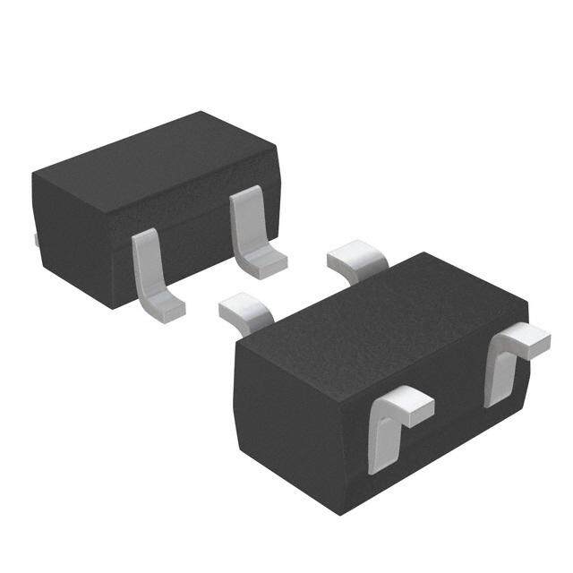
| 供应商器件封装 | 10-MSOP |
| 其它名称 | LTC2918IMSA1PBF |
| 包装 | 管件 |
| 受监控电压数 | 1 |
| 复位 | 低有效 |
| 复位超时 | 最小为 150 ms |
| 安装类型 | 表面贴装 |
| 封装/外壳 | 10-TFSOP,10-MSOP(0.118",3.00mm 宽) |
| 工作温度 | -40°C ~ 85°C |
| 标准包装 | 50 |
| 电压-阈值 | 27 种可选阀值组合 |
| 类型 | 多压监控器 |
| 输出 | 开路漏极或开路集电极 |


- 商务部:美国ITC正式对集成电路等产品启动337调查
- 曝三星4nm工艺存在良率问题 高通将骁龙8 Gen1或转产台积电
- 太阳诱电将投资9.5亿元在常州建新厂生产MLCC 预计2023年完工
- 英特尔发布欧洲新工厂建设计划 深化IDM 2.0 战略
- 台积电先进制程称霸业界 有大客户加持明年业绩稳了
- 达到5530亿美元!SIA预计今年全球半导体销售额将创下新高
- 英特尔拟将自动驾驶子公司Mobileye上市 估值或超500亿美元
- 三星加码芯片和SET,合并消费电子和移动部门,撤换高东真等 CEO
- 三星电子宣布重大人事变动 还合并消费电子和移动部门
- 海关总署:前11个月进口集成电路产品价值2.52万亿元 增长14.8%


PDF Datasheet 数据手册内容提取
LTC2917/LTC2918 Voltage Supervisor with 27 Selectable Thresholds and Watchdog Timer FEATURES DESCRIPTION ■ 9 Selectable Supply Voltages The LTC®2917-A/LTC2917-B and LTC2918-A/LTC2918-B 12V, 5V, 3.3V, 2.5V, 1.8V are low voltage single-supply monitors with selectable 1.5V, 1.2V, 1V, +ADJ (0.5V) thresholds and an adjustable watchdog timer. The parts ■ 3 Selectable Tolerances operate from 1.5V to 5.5V and consume a quiescent cur- –5%, –10%, –15% (LTC2917) rent of only 30μA. ■ Manual Reset Input (LTC2918) Two three state inputs select one of nine internally pro- ■ 1.5V to 5.5V Supply Operation grammed thresholds without the need for external resistors. ■ Adjustable Watchdog Timeout For the LTC2917, an additional three state input determines ■ Windowed Watchdog Timeout for Higher Reliability the tolerance (–5%, –10%, –15%). The tolerance for the Applications (LTC2917-B, LTC2918-B) LTC2918 is fi xed at –5%. Threshold accuracy is guaranteed ■ 6.2V Shunt Regulator for High Voltage Operation at ±1.5% over the entire operating temperature range. ■ Guaranteed Operation to 125°C Glitch fi ltering ensures reliable reset operation without ■ Guaranteed Threshold Accuracy: ±1.5% false triggering. ■ Low Quiescent Current: 30μA Typical ■ Power Supply Glitch Immunity The reset timeout and the watchdog timeout may be set ■ Guaranteed RST for V ≥ 0.8V with no external components, or adjusted using an exter- CC ■ 10-Lead MSOP Packages and (3mm × 2mm) DFN nal capacitor. A windowed watchdog feature is available Packages for high-reliability applications (B1 versions). A separate manual reset input on the LTC2918-A/LTC2918-B allows APPLICATIONS a simple push button interface. ■ Handheld Devices Operation to 125°C makes the LTC2917-A/LTC2917-B ■ Cell Phone Base Stations and LTC2918-A/LTC2918-B suitable for automotive ■ Automotive Control Systems applications. ■ Network Servers , LT, LTC and LTM are registered trademarks of Linear Technology Corporation. ■ Optical Networking Systems All other trademarks are the property of their respective owners. TYPICAL APPLICATION 1.8V Supply Monitor with Manual Monitor Selection Table Reset and Internal Timers Selected NOMINAL VOLTAGE SEL1 SEL2 1.8V 12V V V CC CC 0.1μF 10k 5V VCC Open VCC 3.3V VCC GND LTC2918-A μP 2.5V Open VCC VM RST RST 1.8V Open Open RT WDI I/O 1.5V Open GND WT SEL1 29178 TA01 MR SEL2 1.2V GND V CC GND 1V GND Open tWDU = 1.6s tRST = 200ms ADJ (0.5V) GND GND 29178fb 1
LTC2917/LTC2918 ABSOLUTE MAXIMUM RATINGS (Note 1, 2) Terminal Voltages Operating Temperature Range V (Note 3) ..........................................–0.3V to 5.7V LTC2917C/LTC2918C ...............................0°C to 70°C CC SEL1, SEL2, TOL, WDI, MR, RST .........–0.3V to 7.5V LTC2917I/LTC2918I ..............................–40°C to 85°C VM .........................................................–0.3V to 15V LTC2917H/LTC2918H .........................–40°C to 125°C RT, WT .......................................–0.3V to (V + 0.3)V Storage Temperature Range ...................–65°C to 150°C CC Terminal Currents Lead Temperature (Soldering, 10 sec) V (Note 3) .......................................................±5mA MSOP ...............................................................300°C CC PIN CONFIGURATION LTC2917 LTC2917 TOP VIEW TOP VIEW GND 1 10 RST GND 1 10 RST TOL 2 9 RT TOL 2 9 RT SEL2 3 11 8 WT SEL2 3 8 WT SEL1 4 7 WDI SEL1 4 7 WDI VM 5 6 VCC VM 5 6 VCC MS PACKAGE 10-LEAD PLASTIC MSOP DDB PACKAGE 10-LEAD (3mm (cid:115) 2mm) PLASTIC DFN TJMAX = 125LT°CC2, 9θ1JA7 = 200°C/W TJMAX = 125°C, θJA = 43°C/W EXPOSED PAD (PIN 11) PCB GND CONNECTION OPTIONAL LTC2917 LTC2918 LTC2918 TOP VIEW TOP VIEW GND 1 10 RST GND 1 10 RST MR 2 9 RT MR 2 9 RT SEL2 3 11 8 WT SEL2 3 8 WT SEL1 4 7 WDI SEL1 4 7 WDI VM 5 6 VCC VM 5 6 VCC MS PACKAGE 10-LEAD PLASTIC MSOP DDB PACKAGE 10-LEAD (3mm (cid:115) 2mm) PLASTIC DFN TJMAX = 125LT°CC2, 9θ1JA8 = 200°C/W TJMAX = 125°C, θJA = 43°C/W EXPOSED PAD (PIN 11) PCB GND CONNECTION OPTIONAL LTC2918 29178fb 2
LTC2917/LTC2918 ORDER INFORMATION LEAD FREE FINISH TAPE AND REEL PART MARKING* PACKAGE DESCRIPTION TEMPERATURE RANGE LTC2917CMS-B1#PBF LTC2917CMS-B1#TRPBF LTCQP 10-Lead Plastic MSOP 0°C to 70°C LTC2917IMS-B1#PBF LTC2917IMS-B1#TRPBF LTCQP 10-Lead Plastic MSOP –40°C to 85°C LTC2917HMS-B1#PBF LTC2917HMS-B1#TRPBF LTCQP 10-Lead Plastic MSOP –40°C to 125°C LTC2917CMS-A1#PBF LTC2917CMS-A1#TRPBF LTDGD 10-Lead Plastic MSOP 0°C to 70°C LTC2917IMS-A1#PBF LTC2917IMS-A1#TRPBF LTDGD 10-Lead Plastic MSOP –40°C to 85°C LTC2917HMS-A1#PBF LTC2917HMS-A1#TRPBF LTDGD 10-Lead Plastic MSOP –40°C to 125°C LTC2918CMS-B1#PBF LTC2918CMS-B1#TRPBF LTDCT 10-Lead Plastic MSOP 0°C to 70°C LTC2918IMS-B1#PBF LTC2918IMS-B1#TRPBF LTDCT 10-Lead Plastic MSOP –40°C to 85°C LTC2918HMS-B1#PBF LTC2918HMS-B1#TRPBF LTDCT 10-Lead Plastic MSOP –40°C to 125°C LTC2918CMS-A1#PBF LTC2918CMS-A1#TRPBF LTDGG 10-Lead Plastic MSOP 0°C to 70°C LTC2918IMS-A1#PBF LTC2918IMS-A1#TRPBF LTDGG 10-Lead Plastic MSOP –40°C to 85°C LTC2918HMS-A1#PBF LTC2918HMS-A1#TRPBF LTDGG 10-Lead Plastic MSOP –40°C to 125°C TAPE AND REEL (MINI) TAPE AND REEL PART MARKING* PACKAGE DESCRIPTION TEMPERATURE RANGE LTC2917CDDB-B1#TRMPBF LTC2917CDDB-B1#TRPBF LCQR 10-Lead (3mm × 2mm) Plastic DFN 0°C to 70°C LTC2917IDDB-B1#TRMPBF LTC2917IDDB-B1#TRPBF LCQR 10-Lead (3mm × 2mm) Plastic DFN –40°C to 85°C LTC2917HDDB-B1#TRMPBF LTC2917HDDB-B1#TRPBF LCQR 10-Lead (3mm × 2mm) Plastic DFN –40°C to 125°C LTC2917CDDB-A1#TRMPBF LTC2917CDDB-A1#TRPBF LDGF 10-Lead (3mm × 2mm) Plastic DFN 0°C to 70°C LTC2917IDDB-A1#TRMPBF LTC2917IDDB-A1#TRPBF LDGF 10-Lead (3mm × 2mm) Plastic DFN –40°C to 85°C LTC2917HDDB-A1#TRMPBF LTC2917HDDB-A1#TRPBF LDGF 10-Lead (3mm × 2mm) Plastic DFN –40°C to 125°C LTC2918CDDB-B1#TRMPBF LTC2918CDDB-B1#TRPBF LDCV 10-Lead (3mm × 2mm) Plastic DFN 0°C to 70°C LTC2918IDDB-B1#TRMPBF LTC2918IDDB-B1#TRPBF LDCV 10-Lead (3mm × 2mm) Plastic DFN –40°C to 85°C LTC2918HDDB-B1#TRMPBF LTC2918HDDB-B1#TRPBF LDCV 10-Lead (3mm × 2mm) Plastic DFN –40°C to 125°C LTC2918CDDB-A1#TRMPBF LTC2918CDDB-A1#TRPBF LDGH 10-Lead (3mm × 2mm) Plastic DFN 0°C to 70°C LTC2918IDDB-A1#TRMPBF LTC2918IDDB-A1#TRPBF LDGH 10-Lead (3mm × 2mm) Plastic DFN –40°C to 85°C LTC2918HDDB-A1#TRMPBF LTC2918HDDB-A1#TRPBF LDGH 10-Lead (3mm × 2mm) Plastic DFN –40°C to 125°C TRM = 500 pieces. *Temperature grades are identifi ed by a label on the shipping container. Consult LTC Marketing for information on non-standard lead based fi nish parts. For more information on lead free part marking, go to: http://www.linear.com/leadfree/ For more information on tape and reel specifi cations, go to: http://www.linear.com/tapeandreel/ 29178fb 3
LTC2917/LTC2918 ELECTRICAL CHARACTERISTICS The ● denotes the specifi cations which apply over the full operating temperature range, otherwise specifi cations are at T = 25°C. V = 2.5V, unless otherwise noted. (Note 2) A CC SYMBOL PARAMETER CONDITIONS MIN TYP MAX UNITS V Minimum Supply Voltage RST in Correct Logic State ● 0.8 V CC(MIN) V Supply Undervoltage Lockout ● 1.5 V CC(UVLO) V Shunt Regulation Voltage I = 0.5mA ● 5.7 6.2 7.0 V CC(SHUNT) VCC I V Pin Current SEL1, SEL2, TOL, MR = Open ● 30 50 μA CC CC SEL1, SEL2, TOL = GND (LTC2917) ● 45 80 μA MR = V (LTC2918) CC Monitor Input (VM) V 12V, 5% Reset Threshold ● 11.04 11.22 11.40 V MT120 12V, 10% Reset Threshold ● 10.44 10.62 10.80 V 12V, 15% Reset Threshold ● 9.84 10.02 10.20 V V 5V, 5% Reset Threshold ● 4.600 4.675 4.750 V MT50 5V, 10% Reset Threshold ● 4.350 4.425 4.500 V 5V, 15% Reset Threshold ● 4.100 4.175 4.250 V V 3.3V, 5% Reset Threshold ● 3.036 3.086 3.135 V MT33 3.3V, 10% Reset Threshold ● 2.871 2.921 2.970 V 3.3V, 15% Reset Threshold ● 2.706 2.756 2.805 V V 2.5V, 5% Reset Threshold ● 2.300 2.338 2.375 V MT25 2.5V, 10% Reset Threshold ● 2.175 2.213 2.250 V 2.5V, 15% Reset Threshold ● 2.050 2.088 2.125 V V 1.8V, 5% Reset Threshold ● 1.656 1.683 1.710 V MT18 1.8V, 10% Reset Threshold ● 1.566 1.593 1.620 V 1.8V, 15% Reset Threshold ● 1.476 1.503 1.530 V V 1.5V, 5% Reset Threshold ● 1.380 1.403 1.425 V MT15 1.5V, 10% Reset Threshold ● 1.305 1.328 1.350 V 1.5V, 15% Reset Threshold ● 1.230 1.253 1.275 V V 1.2V, 5% Reset Threshold ● 1.104 1.122 1.140 V MT12 1.2V, 10% Reset Threshold ● 1.044 1.062 1.080 V 1.2V, 15% Reset Threshold ● 0.984 1.002 1.020 V V 1V, 5% Reset Threshold ● 0.920 0.935 0.950 V MT10 1V, 10% Reset Threshold ● 0.870 0.885 0.900 V 1V, 15% Reset Threshold ● 0.820 0.835 0.850 V V ADJ (0.5V), 5% Reset Threshold ● 460.0 467.5 475.0 mV MTADJ ADJ (0.5V), 10% Reset Threshold ● 435.0 442.5 450.0 mV ADJ (0.5V), 15% Reset Threshold ● 410.0 417.5 425.0 mV RVM VM Input Impedance (Note 4) Fixed Threshold Modes ● 0.5 8 MΩ I ADJ Input Current VM = 0.5V ● ±15 nA VM(ADJ) Three-State Inputs (SEL1, SEL2), (TOL, LTC2917) V Low Level Input Voltage ● 0.5 V TPIN,LOW V High Level Input Voltage ● 1.4 V TPIN,HIGH V Pin Voltage when Open I = 0μA 0.9 V TPIN,Z I Allowable Leakage in Open State ● ±5 μA TPIN,Z I Pin Input Current V = 0V, V ● ±20 μA TPIN,H/L TPIN CC Reset Timer Control (RT) I RT Pull-Up Current V = 0.25V ● –2 –3 –4 μA RT(UP) RT I RT Pull-Down Current V = 1.1V ● 2 3 4 μA RT(DOWN) RT I Internal RT V Detect Current V = V ● 1 8 μA RT(INT) CC RT CC V RT Internal Timer Threshold V Rising, Referenced to V ● –100 –160 –300 mV RT(INT, LH) RT CC 29178fb 4
LTC2917/LTC2918 ELECTRICAL CHARACTERISTICS The ● denotes the specifi cations which apply over the full operating temperature range, otherwise specifi cations are at T = 25°C. V = 2.5V, unless otherwise noted. (Note 2) A CC SYMBOL PARAMETER CONDITIONS MIN TYP MAX UNITS Reset Output (RST) t Internal Reset Timeout Period V = V ● 150 200 260 ms RST(INT) RT CC t Adjustable Reset Timeout Period C = 2.2nF ● 16 20 25 ms RST(EXT) RT t VM Undervoltage Detect to RST VM Less Than Reset Threshold ● 10 80 150 μs UV Asserted V by More Than 5% MTX V Output Voltage Low RST V = 3.3V, I = 2.5mA ● 0.15 0.4 V OL CC RST V = 1V, I = 100μA ● 0.15 0.3 V CC RST V = 0.8V, I = 15μA ● 0.05 0.2 V CC RST I RST Output Voltage High Leakage RST = V ● ±1 μA OH(RST) CC Watchdog Timer Control (WT) I WT Pull-Up Current V = 0.25V ● –2 –3 –4 μA WT(UP) WT I WT Pull-Down Current V = 1.1V ● 2 3 4 μA WT(DOWN) WT V WT Internal Timer Threshold V Rising, Referenced to V ● –100 –160 –300 mV WT(INT, LH) WT CC I Internal WT V Detect Current V = V ● 1 8 μA WT(INT) CC WT CC I Watchdog Disable Hold Current V = 0V –3.5 μA WT(DIS) WT Watchdog Input (WDI) t Internal Watchdog Upper Boundary V = V ● 1.3 1.6 2 s WDU(INT) WT CC t Internal Watchdog Lower Boundary B Versions, V = V ● 37.5 50 62.5 ms WDL(INT) WT CC (Note 5) t External Watchdog Upper Boundary C = 2.2nF ● 130 160 200 ms WDU(EXT) WT t External Watchdog Lower Boundary B Versions, C = 2.2nF ● t /32 ms WDL(EXT) WT WDU(EXT) (Note 5) V Input Low Voltage ● 0.4 V IL(WDI) V Input High Voltage ● 1.1 V IH(WDI) t Input Pulsewidth ● 400 ns PW(WDI) WDI Leakage Current ● ±1 μA Manual Reset Input (LTC2918) V Input Low Voltage ● 0.2 • V V IL(MR) CC V Input High Voltage ● 0.8 • V V IH(MR) CC RPU Pull-Up Resistance ● 50 100 150 kΩ t Pulsewidth ● 250 ns PW(MR) Note 1: Stresses beyond those listed under Absolute Maximum Ratings from higher voltage supplies requires a series dropping resistor. See may cause permanent damage to the device. Exposure to any Absolute Applications Information. Maximum Rating condition for extended periods may affect device Note 4: Input impedance is dependent on the confi guration of the SEL reliability and lifetime. pins. Note 2: All currents into pins are positive; all voltages are referenced to Note 5: In the LTC2917-B/LTC2918-B, edges must occur on WDI with a GND unless otherwise noted. period between the lower and upper boundary or RST is invoked. For the Note 3: V maximum pin voltage is limited by input current. Since the LTC2917-A/LTC2918-A, the edges must simply occur before the upper CC V pin has an internal 6.2V shunt regulator, a low impedance supply boundary. See Applications Information. CC which exceeds 5.7V may exceed the rated terminal current. Operation 29178fb 5
LTC2917/LTC2918 TYPICAL PERFORMANCE CHARACTERISTICS Threshold Voltage vs Quiescent Supply Current vs Allowable Glitch Duration vs Temperature Temperature Magnitude 1.5 40 s)300 SEL1 = 0V μ A) SEL2 = 2.5V N ( μ O (%)MTnn 10..05 VMTADJ RRENT, I (CC 35 TOL = OPEN VCC = 5.5V TCH DURATI220500 RESET OCCURS NORMALIZED V ––01..500 VMT25 VMT120 ESCENT SUPPLY CU 2350 VVCCCC == 21..55VV UM ALLOWABLE GLI11505000 ABOVE CURVE UI M Q XI A –1.5 20 M 0 –50 –25 0 25 50 75 100 125 –50 –25 0 25 50 75 100 125 0.1 1 10 100 TEMPERATURE (°C) TEMPERATURE (°C) GLITCH PERCENTAGE PAST THRESHOLD (%) 29178 G01 29178 G02 29178 G03 Reset Timeout Period vs RT Internal Reset Timeout Period vs Internal Watchdog Timeout Capacitance Temperature Period vs Temperature 10000 250 2.0 OD, t (ms)RST(EXT)1100000 OD, t (ms)RST(INT)221300 RT = VCC RIOD, t (ms)WDU(INT)11..68 WT = VCC RI RI PE OUT PE 10 OUT PE190 MEOUT 1.4 ME ME TI RESET TI 1 RESET TI170 ATCHDOG 1.2 0.1 150 W 1.0 0.001 0.01 0.1 1 10 100 1000 –50 –25 0 25 50 75 100 125 –50 –25 0 25 50 75 100 125 RT PIN CAPACITANCE, CRT (nF) TEMPERATURE (°C) TEMPERATURE (°C) 29178 G04 29178 G05 29178 G06 Watchdog Timeout Period vs Shunt Regulation Voltage vs Shunt Regulation Voltage vs Capacitance Temperature Supply Current (ms)WDU(EXT)110000000 V (V)CC(SHUNT)6.4 ICC = 5mA V (V)CC(SHUNT) 76..08 OUT PERIOD, t 100 ON VOLTAGE, 6.3 ICC = 1mA ON VOLTAGE, 66..46 ME ATI 6.2 ICC = 100μA ATI G TI 10 GUL GUL DO RE RE 6.2 WATCH 1 SHUNT 6.1 SHUNT 6.0 0.001 0.01 0.1 1 10 100 –50 –25 0 25 50 75 100 125 0.01 0.1 1 10 100 WT PIN CAPACITANCE, CWT (nF) TEMPERATURE (°C) SUPPLY CURRENT, ICC (mA) 29178 G07 29178 G08 29178 G09 29178fb 6
LTC2917/LTC2918 TYPICAL PERFORMANCE CHARACTERISTICS RST Output Voltage vs VCC RST Pull-Down Current vs VCC RST VOL vs IRST 6 6 1.0 10k PULL-UP R TO VCC NO PULL-UP R SEL1 = SEL2 = TOL = 0V VCC = 2.5V 5 VM = 0.5V mA) 5 0.8 RST VOLTAGE (V) 234 OWN CURRENT, I (RST 234 RST AT 150mV RST VOLTAGE (V) 00..46 TA = 25°C TA = 125°C D LL- 0.2 1 PU 1 RST AT 50mV TA = –40°C 0 0 0 0 1 2 3 4 5 0 1 2 3 4 5 0 2 4 6 8 10 SUPPLY VOLTAGE, VCC (V) SUPPLY VOLTAGE, VCC (V) IRST (mA) 29178 G10 29178 G11 29178 G12 PIN FUNCTIONS GND: Device Ground. that the part is out of under voltage lockout and that the voltage thresholds are accurate. Operates as a direct supply MR (LTC2918 only): Manual Reset Input (Active Low). A low input for voltages up to 5.5V. Operates as a shunt regulator level on the MR input causes the part to issue a reset, which for supply voltages greater than 5.7V and should have a is released one reset timeout after the input goes high. The pin resistor between this pin and the supply to limit V input has an internal 100k pull-up to V , and thus may interface CC CC current to no greater than 5mA. When used without a cur- directly to a momentary pushbutton. Leave open if unused. rent-limiting resistor, pin voltage must not exceed 5.7V. RST: Open Drain RST Output. Asserts low when VM is VM: Voltage Monitor Input to RST comparator. SEL1, SEL2 below the threshold selected by SEL1, SEL2 and TOL input and TOL inputs select the exact threshold that asserts the pins. Held low for an adjustable timeout after VM input is RST output. above threshold. WDI: Watchdog Input. This pin must be driven to change RT: Reset Timeout Control Pin. Attach an external capacitor state within a time less than the watchdog upper bound- (C ) to GND to set a reset timeout of 9ms/nF. Leave RT open RT ary time, or RST will be asserted low. On the LTC2917-B, to generate a reset timeout of approximately 400μs. Tie RT to LTC2918-B, the period must also be greater than the V to generate a reset timeout of approximately 200ms. CC watchdog lower boundary time, and only falling edges SEL1, SEL2: Monitor Voltage Select Three-State Input. are considered. Tie WT and WDI to GND to disable the SEL1, and SEL2 control the nominal threshold voltage watchdog timer. that VM is set to monitor. Connect to V , GND or leave CC WT: Watchdog Timer Control Pin. Attach an external unconnected in open state. (See Table 1). capacitor (C ) to GND to set a watchdog upper bound- WT TOL (LTC2917 only): Three-State Input for Supply Tolerance ary timeout time of 72ms/nF. Tie WT to V to generate a CC Selection (–5%, –10% or –15%). Controls the tolerance timeout of approximately 1.6s. Leave WT open to generate band at which the VM supply is monitored. Connect to VCC, a timeout of approximately 3.2ms. Tie WT and WDI to GND GND, or leave unconnected in open state. (See Table 2) to disable the watchdog timer. VCC: Power Supply input. Bypass this pin to ground with a Exposed Pad (DFN Only): Exposed Pad may be left open 0.1μF ceramic capacitor. A minimum of 1.5V on VCC ensures or connected to device ground. 29178fb 7
LTC2917/LTC2918 BLOCK DIAGRAM LTC2917 LTC2918 SEL1 SEL2 TOL MR RT 3 STATE VCC VCC DETECT VCC VCC DECODE 100k 6.2V MONITOR INTERNAL VM RST DIVIDER 200ms TIMER MATRIX – RESET + DRIVER LOGIC REFERENCE GND DIVIDER ADJUSTABLE + MATRIX RESET TIMER – 0.5V INTERNAL 1.6 SECOND TIMER WATCHDOG LOGIC ADJUSTABLE WATCHDOG TIMER VCC DETECT WT WDI 29178 BD TIMING DIAGRAMS Monitor Input Timing VM VMTx tUV tRST RST 1V 29178 TD01 Watchdog Timing (LTC2917-A, LTC2918-A) WDI RST tWDU 29178 TD01 tRST Watchdog Timing (LTC2917-B, LTC2918-B) WDI RST t > tWDL tWDU 29178 TD03 t < tWDL tRST tRST 29178fb 8
LTC2917/LTC2918 APPLICATIONS INFORMATION Supply Monitoring Monitor Threshold Control The LTC2917/LTC2918 are low voltage single supply The monitor threshold on the VM pin is controlled by monitors with selectable thresholds. Two three-state inputs the SEL1, SEL2 and TOL three-state pins. The SEL1 and select one of nine internally programmed thresholds. For SEL2 pins select one of nine preset nominal voltages the LTC2917, a third three-state input selects the tolerance (including one externally adjustable threshold) as shown at which the supply connected to the VM pin is monitored in Table 1. (–5%, –10%, –15%). The tolerance for the LTC2918 is The SEL1 and SEL2 three-state input pins should be con- fi xed at –5%. Threshold accuracy is guaranteed at ±1.5% nected to GND, V or left unconnected during normal CC over the entire operating temperature range. operation. Note that when left unconnected, the maximum The LTC2917/LTC2918 asserts the RST output low when leakage allowable from the pin to either GND or V is CC VM is below the programmed threshold, and for a reset ±5μA. timeout period (t ) after VM goes above the threshold. RST The tolerance at which the monitored supply is measured The reset timeout can be confi gured to use one of two is set by the TOL pin (LTC2917 only) as shown in Table 2. internal timers with no external components, or an ad- If desired (e.g. for margining purposes), the TOL pin may justed timer programmed by placing an external capacitor be driven by a three-state buffer. That three-state buffer from RT to ground. Glitch fi ltering ensures reliable reset must have a V and V which meet the V and V of OL OH IL IH operation without false triggering. the TOL pin specifi ed in the Electrical Characteristics, and maintain less than 5μA of leakage in the open state. Power-Up V powers the drive circuits for the RST pin. Therefore, Table 1. Voltage Threshold Settings CC as soon as V reaches 0.8V during power up, the RST NOMINAL VOLTAGE SEL1 SEL2 CC output asserts low. 12V V V CC CC 5V V Open Until V reaches the undervoltage lockout threshold CC CC 3.3V V GND (guaranteed less than 1.5V), RST is held low regardless CC of the state of VM. 2.5V Open VCC 1.8V Open Open Once V is above the undervoltage lockout threshold CC *1.5V Open GND and VM is above the programmed threshold, the reset *1.2V GND V timer is started. After the reset timeout, the open drain CC *1V GND Open pull-down releases RST and the external pull-up resistor *ADJ (0.5V) GND GND pulls high. *Require a separate supply for V CC Power-Down Table 2. System Voltage Tolerance Settings On power-down, once VM drops below its threshold or TOLERANCE TOL V drops below the undervoltage lockout, RST asserts CC –5% VCC logic low. –10% Open –15% GND 29178fb 9
LTC2917/LTC2918 APPLICATIONS INFORMATION Threshold Accuracy Two techniques are used to combat spurious reset without sacrifi cing threshold accuracy. First, the timeout period The trip threshold for the supplies monitored is selected helps prevent high-frequency variation whose frequency by confi guring the three-state input pins. When using the is above 1/ t from appearing at the RST output. adjustable input, a external resistive divider sets the trip RST threshold, allowing the user complete control over the When the voltage at VM goes below the threshold, the trip point. Selection of this trip voltage is crucial to the RST pin asserts low. When the supply recovers past reliability of the system. the threshold, the reset timer starts (assuming it is not disabled), and RST does not go high until it fi nishes. If Any power supply has some tolerance band within which the supply becomes invalid any time during the timeout it is expected to operate (e.g. 5V±10%). It is generally period, the timer resets and starts a fresh when the supply undesirable that a supervisor issue a reset when the power next becomes valid. supply is inside this tolerance band. Such a “nuisance” reset reduces reliability by preventing the system from While the reset timeout is useful at preventing toggling functioning under normal conditions. of the reset output in most cases, it is not effective at preventing nuisance resets due to short glitches (due to To prevent nuisance resets, the supervisor threshold must load transients or other effects) on a valid supply. be guaranteed to lie outside the power supply tolerance band. To ensure that the threshold lies outside the power To reduce sensitivity to these short glitches, the comparator supply tolerance range, the nominal threshold must lie out- has additional anti-glitch circuitry. Any transient at the input side that range by the monitor’s accuracy specifi cation. of the comparator needs to be of suffi cient magnitude and duration t before it can change the monitor state. All 27 of the selectable thresholds have the same relative UV threshold accuracy of ±1.5% of the programmed nominal The combination of the reset timeout and anti-glitch cir- input voltage (over the full operating temperature range). cuitry prevents spurious changes in output state without Consider the example of monitoring a 5V supply with a 10% sacrifi cing threshold accuracy. tolerance. The nominal threshold internal to the LTC2917 is 11.5% below the 5V input at 4.425V. With ±1.5% ac- Adjustable Input curacy, the trip threshold range is 4.425V±75mV over When the monitor threshold is confi gured as ADJ, the temperature (i.e. 10% to 13% below 5V). The monitored internal comparator input is connected to the pin without system must thus operate reliably down to 4.35V or 13% a resistive divider, and the pin is high-impedance. Thus, below 5V over temperature. any desired threshold may be chosen by attaching VM to a tap point on an external resistive divider between the Glitch Immunity monitored supply and ground, as shown in Figure 1. The above discussion is concerned only with the DC value of the monitored supply. Real supplies also have VMON relatively high-frequency variation, from sources such as R2 load transients, noise, and pickup. These variations should VM – not be considered by the monitor in determining whether a supply voltage is valid or not. The variations may cause R1 + spurious outputs at RST, particularly if the supply voltage +– 0.5V is near its trip threshold. 29178 F01 Figure 1. Setting the Trip Point Using the Adjustable Threshold. 29178fb 10
LTC2917/LTC2918 APPLICATIONS INFORMATION The reference input of the comparator is controlled by the 10000 s) tolerance pin. The external resistive divider should make m (T)1000 the voltage at VM = 0.5V when the supply is at nominal X E T ( value. The actual threshold of VM accounts for the sup- S R ply tolerance of ±1.5% guaranteed over the full operating D, t 100 O RI temperature range. The resulting tolerances are –6.5%, E T P 10 –11.5%, –16.5% which correspond to 0.468V, 0.443V, OU E M 0.418V respectively. T TI 1 E S Typically, the user will pick a value of R1 based on accept- E R 0.1 able current draw. Current used by the resistor divider will 0.001 0.01 0.1 1 10 100 1000 be approximately: RT PIN CAPACITANCE, CRT (nF) 29178 F02 ⎛0.5V⎞ R1=⎜ ⎟ Figure 2. Reset Timeout Period vs RT Capacitance ⎝ ⎠ I RST Output Characteristics Recommended range of R1 is 1k—1M. Higher values of The DC characteristics of the RST pull-down strength resistance exacerbate the degradation of threshold ac- are shown in the Typical Performance Characteristics curacy due to leakage currents. section. RST is an open-drain pin and thus requires an If the nominal value of the supply being monitored is external pull-up resistor to the logic supply. RST may be VNOM, then pulled above VCC, providing the voltage limits of the pin are observed. R2 = R1(2V – 1) NOM The open-drain of the RST pin allows for wired-OR con- Resistor tolerances must be taken into account when nection of several LTC2917/LTC2918’s. determining the overall accuracy. Watchdog Selecting the Reset Timing Capacitor LTC2917-A/LTC2918-A The reset timeout period can be set to one of two fi xed internal timers or set with a capacitor in order to accom- A standard watchdog function is used to ensure that the modate a variety of applications. Connecting a capacitor, system is in a valid state by continuously monitoring CRT, between the RT pin and ground sets the reset timeout the microprocessor’s activity. The microprocessor must period, tRST. The following formula approximates the value toggle the logic state of the WDI pin periodically (within of capacitor needed for a particular timeout: upper boundary) in order to clear the watchdog timer. If timeout occurs, the LTC2917-A/LTC2918-A asserts RST C = t • 110 [pF/ms] RT RST low for the reset timeout period, issuing a system reset. For example, using a standard capacitor value of 2.2nF Once the reset timeout completes, RST is released to go would give a 20ms timeout. high and the watchdog timer starts again. Figure 2 shows the desired reset timeout period as a During power-up, the watchdog timer remains cleared while function of the value of the timer capacitor. RST is asserted low. As soon as the reset timer times out, Leaving RT open with no external capacitor generates a RST goes high and the watchdog timer is started. reset timeout of approximately 400μs. Shorting RT to V CC generates a reset timeout of approximately 200ms. 29178fb 11
LTC2917/LTC2918 APPLICATIONS INFORMATION LTC2917-B/LTC2918-B Manual Reset (LTC2918 Only) For applications in which reliability is even more critical, The LTC2918 includes the MR pin for applications where a the LTC2917-B/LTC2918-B implements a windowed watch- manual reset is desired. MR is internally pulled up, making dog function by adding a lower boundary condition to the it ready to interface with a push button with no external standard watchdog function. If the WDI input receives a components required. Asserting MR low when RST is high falling edge prior to the watchdog lower boundary, the initiates a reset, resulting in RST being asserted low for part considers this a watchdog failure, and asserts RST the reset timeout time. low (releasing again after the reset timeout period as described above). The LTC2917-B/LTC2918-B WDI input Shunt Regulator only responds to falling edges. The LTC2917 and LTC2918 contain an internal 6.2V shunt regulator on the V pin to allow operation from a high CC Setting the Watchdog Timeout Period voltage supply. To operate the part from a supply higher The watchdog timeout period is adjustable and can be than 5.7V, the V pin must have a series resistor, R , CC CC optimized for software execution. The watchdog timeout to the supply. See Figure 3. This resistor should be sized period is adjusted by connecting a capacitor between WT according to the following equation: and ground. Given a specifi ed watchdog timeout period, V −5.7V V −7V the capacitor is determined by: S(MAX) ≤R ≤ S(MIN) 5mA CC 250μA C = t • 13.8 [nF/s] WT WD where V and V are the operating minimum S(MIN) S(MAX) For example, using a standard capacitor value of 0.047μF and maximum of the supply. would give a 3.4s watchdog timeout period. As an example, consider operation from an automobile Leaving WT open with no external capacitor generates battery which might dip as low as 10V or spike to 60V. We a timeout of approximately 3.2ms. Shorting WT to V must then pick a resistance between 10.86k and 12k. CC generates a timeout of approximately 1.6s. Connecting WT to GND disables the watchdog function. (VTRIP = 10.64V) 12V 3.3V R2 RCC RPU 1.15M 11k 10k CBYPASS VCC 0.1μF VCC LTC2917 μP VM RST RST SEL1 WDI I/O GND R1 SEL2 29178 F03 49.9k TOL GND WT RT CWT CRT Figure 3. 12V Supply Monitor Powered From 12V, Utilizing the Internal Shunt Regulator with 3.3V Logic Out 29178fb 12
LTC2917/LTC2918 TYPICAL APPLICATIONS 1V Supply Monitor with Windowed Watchdog Timeout 12V Supply Monitor with 20ms Reset Timeout and 3.4s and Internal Timers Selected Watchdog Timeout, with 3.3V Logic Out 3.3V 3.3V CBYPASS RPU CBYPASS RPU 0.1μF 10k 0.1μF 10k VCC VCC VCC VCC LTC2917-B μP LTC2917-A μP 1V VM RST RST 12V VM RST RST SEL1 WDI I/O GND SEL1 WDI I/O GND SEL2 29178 TA02 SEL2 29178 TA03 TOL TOL GND WT RT GND WT RT 3.3V tWDU = 1.6s CWT CRT tWDL = 50ms 0.047μF 0.0022μF tRST = 200ms 9V, –15% Tolerance Supply Monitor ith 1.8V Logic Out 1.8V CBYPASS RPU 9V 0.1μF 10k R2 VCC VCC 866k LTC2917-A μP VM RST RST SEL1 WDI I/O GND R1 SEL2 29178 TA04 51.1k TOL GND WT RT CWT CRT 29178fb 13
LTC2917/LTC2918 TYPICAL APPLICATIONS 3.3V, –10% Tolerance Supply Monitor with Disabled Watchdog 1.8V, –5% Supply Monitor with Manual Reset 3.3V 1.8V CBYPASS RPU CBYPASS RPU 0.1μF 10k 0.1μF 10k VCC VCC VCC VCC LTC2917 μP LTC2918 μP VM RST RST VM RST RST SEL1 WDI GND SEL1 WDI I/O GND SEL2 29178 TA06 SEL2 29178 TA07 TOL MR GND WT RT 10k* GND WT RT CRT MANUAL RESET PUSHBUTTON CWT CRT *OPTIONAL RESISTOR RECOMMENDED TO EXTEND ESD TOLERANCE 1.5V Supply Monitor with Tolerance Control for Margining, –5% Operation with –15% Margining 3.3V CBYPASS RPU 0.1μF 10k VCC VCC LTC2917 μP 1.5V VM RST RST SEL1 WDI I/O SEL2 TOL I/O GND –15% –5% 29178 TA08 GND WT RT CWT CRT 29178fb 14
LTC2917/LTC2918 PACKAGE DESCRIPTION MS Package 10-Lead Plastic MSOP (Reference LTC DWG # 05-08-1661) 3.00(cid:112) 0.102 (.118(cid:112) .004) 0.497(cid:112) 0.076 (NOTE 3) (.0196(cid:112) .003) 10 9 8 76 REF 3.00(cid:112) 0.102 4.90(cid:112) 0.152 0.254 DETAIL “A” (.193(cid:112) .006) (.1(1N8O(cid:112)TE . 040)4) 0.889(cid:112) 0.127 (.010) 0° – 6° TYP (.035(cid:112) .005) GAUGE PLANE 1 2 3 4 5 0.53(cid:112) 0.152 5.23 (.206) 3.20 – 3.45 (.021(cid:112) .006) 1.10 0.86 MIN (.126 – .136) (.043) (.034) DETAIL “A” MAX REF 0.18 (.007) 0.305(cid:112) 0.038 0.50 SEATING (.0120TY(cid:112)P .0015) (.0B1S9C7) PLANE 0.17 – 0.27 0.1016(cid:112) 0.0508 RECOMMENDED SOLDER PAD LAYOUT (.007 – .011) 0.50 (.004(cid:112) .002) TYP (.0197) MSOP (MS) 0307 REV E NOTE: BSC 1. DIMENSIONS IN MILLIMETER/(INCH) 2. DRAWING NOT TO SCALE 3. DIMENSION DOES NOT INCLUDE MOLD FLASH, PROTRUSIONS OR GATE BURRS. MOLD FLASH, PROTRUSIONS OR GATE BURRS SHALL NOT EXCEED 0.152mm (.006") PER SIDE 4. DIMENSION DOES NOT INCLUDE INTERLEAD FLASH OR PROTRUSIONS. INTERLEAD FLASH OR PROTRUSIONS SHALL NOT EXCEED 0.152mm (.006") PER SIDE 5. LEAD COPLANARITY (BOTTOM OF LEADS AFTER FORMING) SHALL BE 0.102mm (.004") MAX DDB Package 10-Lead Plastic DFN (3mm × 2mm) (Reference LTC DWG # 05-08-1722 Rev Ø) 0.64(cid:112)(cid:0)0.05 3.00(cid:112)(cid:0)0.10 R = 0.115 0.40(cid:112)(cid:0)0.10 (2 SIDES) R = 0.05 TYP (2 SIDES) TYP 6 10 0.70(cid:112)(cid:0)0.05 2.55(cid:112)(cid:0)0.05 2.00(cid:112)(cid:0)0.10 1.15(cid:112)(cid:0)0.05 PIN 1 BAR (2 SIDES) PIN 1 TOP MARK R = 0.20 OR PACKAGE (SEE NOTE 6) 0.64(cid:112) 0.05 0.25(cid:0)(cid:115)(cid:0)45° OUTLINE (2 SIDES) 5 1 CHAMFER (DDB10) DFN 0905 REV Ø 0.25(cid:112)(cid:0)0.05 0.200 REF 0.75(cid:112)(cid:0)0.05 0.25(cid:112) 0.05 0.50 BSC 0.50 BSC 2.39(cid:112)(cid:0)0.05 2.39(cid:112)(cid:0)0.05 (2 SIDES) (2 SIDES) 0 – 0.05 RECOMMENDED SOLDER PAD PITCH AND DIMENSIONS BOTTOM VIEW—EXPOSED PAD NOTE: 1. DRAWING CONFORMS TO VERSION (WECD-1) IN JEDEC PACKAGE OUTLINE M0-229 2. DRAWING NOT TO SCALE 3. ALL DIMENSIONS ARE IN MILLIMETERS 4. DIMENSIONS OF EXPOSED PAD ON BOTTOM OF PACKAGE DO NOT INCLUDE MOLD FLASH. MOLD FLASH, IF PRESENT, SHALL NOT EXCEED 0.15mm ON ANY SIDE 5. EXPOSED PAD SHALL BE SOLDER PLATED 6. SHADED AREA IS ONLY A REFERENCE FOR PIN 1 LOCATION ON THE TOP AND BOTTOM OF PACKAGE 29178fb Information furnished by Linear Technology Corporation is believed to be accurate and reliable. 15 However, no responsibility is assumed for its use. Linear Technology Corporation makes no representa- tion that the interconnection of its circuits as described herein will not infringe on existing patent rights.
LTC2917/LTC2918 TYPICAL APPLICATION Dual Supply Monitor (1.8V and 12V) with Manual Reset 1.8V CBYPASS C1 RPU 0.1μF 0.1μF 10k VCC VCC VCC LTC2916 LTC2917-B μP VM RST 12V VM RST RST SEL1 SEL1 WDI I/O GND SEL2 SEL2 29178 TA10 MR TOL GND RT GND WT RT MANUAL RESET PUSH BUTTON 1.8V 1.8V RELATED PARTS PART NUMBER DESCRIPTION COMMENTS LTC690 5V Supply Monitor, Watchdog Timer and Battery Backup 4.65V Threshold LTC694-3.3 3.3V Supply Monitor, Watchdog Timer and Battery Backup 2.9V Threshold LTC1232 5V Supply Monitor, Watchdog Timer and Push-Button Reset 4.37V/4.62V Threshold LTC1326 Micro Power Precision Triple Supply Monitor 4.725V, 3.118V, 1V Threshold (±0.75%) LTC1536 Precision Triple Supply Monitor for PCI Applications Meets PCI tFALL Timing Specifi cations LTC1726 Micro Power Triple Supply Monitor for 2.5V/5V, 3.3V and ADJ Adjustable RESET and Watchdog Time-Outs LTC1727 Micro Power Triple Supply Monitor with Open-Drain Reset Individual Monitor Outputs in MSOP LTC1728 Micro Power Triple Supply Monitor with Open-Drain Reset 5-Lead SOT-23 Package LTC2900 Programmable Quad Supply Monitor Adjustable RESET, 10-Lead MSOP and 3mm × 3mm 10-Lead DFN LTC2901 Programmable Quad Supply Monitor Adjustable RESET and Watchdog Timer, 16-Lead SSOP Package LTC2902 Programmable Quad Supply Monitor Adjustable RESET and Tolerance, 16-Lead SSOP Package, Margining LTC2903 Precision Quad Supply Monitor 6-Lead SOT-23 Package, Ultra Low Voltage Reset LTC2904 3-State Programmable Precision Dual Supply Monitor Adjustable Tolerance, 8-Lead SOT-23 Package LTC2905 3-State Programmable Precision Dual Supply Monitor Adjustable RESET and Tolerance, 8-Lead SOT-23 Package LTC2906 Precision Dual Supply Monitor 1 Selectable and 1 Adjustable Separate V Pin, RST/RST Outputs CC LTC2907 Precision Dual Supply Monitor 1 Selectable and 1 Adjustable Separate V Pin, Adjustable Reset Timer CC LTC2908 Precision Six Supply Monitor (Four Fixed and 2 Adjustable) 8-Lead SOT-23 and DDB Packages LTC2909 Precision Triple/Dual Input UV, OV 2 ADJ Inputs LTC2910 Octal Positive/Negative Voltage Monitor 16-Lead SSOP and 5mm × 3mm DFN Packages LTC2912 Single UV/OV Voltage Monitor, Adjustable UV and OV 8-Lead TSOT and 3mm × 2mm DFN Packages LTC2913 Dual UV/OV Voltage Monitor 10-Lead MSOP and 3mm × 3mm DFN Packages LTC2914 Qual UV/OV Positive/Negative Voltage Monitor 16-Lead SSOP and 5mm × 3mm DFN Packages LTC2915 Single Supervisor with 27 Selectable Thresholds 10-Lead MSOP and 3mm × 2mm DFN-10 Packages LTC2916 Single Supervisor with 9 Selectable Thresholds Manual Reset, 10-Lead MSOP and 3mm × 2mm DFN-10 Packages 29178fb 16 Linear Technology Corporation LT 0208 REV B • PRINTED IN USA 1630 McCarthy Blvd., Milpitas, CA 95035-7417 (408) 432-1900 ● FAX: (408) 434-0507 ● www.linear.com © LINEAR TECHNOLOGY CORPORATION 2007
Mouser Electronics Authorized Distributor Click to View Pricing, Inventory, Delivery & Lifecycle Information: A nalog Devices Inc.: LTC2918CMS-B1#TRPBF LTC2917IMS-A1#TRPBF LTC2918CDDB-A1#PBF LTC2917HDDB-A1#TRMPBF LTC2918CMS-A1#PBF LTC2917IDDB-B1#TRMPBF LTC2918IDDB-A1#TRPBF LTC2917CDDB-A1#TRPBF LTC2917HDDB-B1#TRPBF LTC2918CDDB-A1#TRMPBF LTC2917HDDB-A1#PBF LTC2917HMS-B1#PBF LTC2918IMS-A1#PBF LTC2917CMS-A1#PBF LTC2918HDDB-A1#TRMPBF LTC2918IMS-A1#TRPBF LTC2918IDDB-B1#TRMPBF LTC2918IDDB-A1#PBF LTC2917CDDB-A1#PBF LTC2917HMS-A1#PBF LTC2917CMS-A1#TRPBF LTC2918HDDB-B1#TRPBF LTC2918HMS-B1#PBF LTC2917CDDB-B1#TRPBF LTC2917IMS-B1#PBF LTC2917CDDB-B1#PBF LTC2917HMS-A1#TRPBF LTC2917IMS-B1#TRPBF LTC2918IDDB- B1#PBF LTC2918IMS-B1#PBF LTC2917IDDB-A1#PBF LTC2917HDDB-A1#TRPBF LTC2917IDDB-B1#TRPBF LTC2918CDDB-B1#PBF LTC2917IDDB-A1#TRMPBF LTC2918HMS-B1#TRPBF LTC2917CMS-B1#PBF LTC2917IDDB-A1#TRPBF LTC2918CMS-A1#TRPBF LTC2918IMS-B1#TRPBF LTC2918IDDB-A1#TRMPBF LTC2917CDDB-A1#TRMPBF LTC2917IMS-A1#PBF LTC2918CMS-B1#PBF LTC2918HMS-A1#TRPBF LTC2918CDDB-B1#TRPBF LTC2917IDDB-B1#PBF LTC2918IDDB-B1#TRPBF LTC2918HDDB-A1#PBF LTC2918HDDB-B1#TRMPBF LTC2917CDDB-B1#TRMPBF LTC2917HDDB-B1#PBF LTC2917HMS-B1#TRPBF LTC2918CDDB-B1#TRMPBF LTC2918HDDB-B1#PBF LTC2917HDDB-B1#TRMPBF LTC2918CDDB-A1#TRPBF LTC2918HDDB-A1#TRPBF LTC2918HMS-A1#PBF LTC2917CMS-B1#TRPBF