ICGOO在线商城 > 集成电路(IC) > 数据采集 - 数模转换器 > LTC2640AITS8-HZ12#TRMPBF

 Datasheet下载
- 型号: LTC2640AITS8-HZ12#TRMPBF
- 制造商: LINEAR TECHNOLOGY
- 库位|库存: xxxx|xxxx
- 要求:
| 数量阶梯 | 香港交货 | 国内含税 |
| +xxxx | $xxxx | ¥xxxx |
查看当月历史价格
查看今年历史价格
LTC2640AITS8-HZ12#TRMPBF产品简介:
ICGOO电子元器件商城为您提供LTC2640AITS8-HZ12#TRMPBF由LINEAR TECHNOLOGY设计生产,在icgoo商城现货销售,并且可以通过原厂、代理商等渠道进行代购。 LTC2640AITS8-HZ12#TRMPBF价格参考。LINEAR TECHNOLOGYLTC2640AITS8-HZ12#TRMPBF封装/规格:数据采集 - 数模转换器, 12 位 数模转换器 1 TSOT-23-8。您可以下载LTC2640AITS8-HZ12#TRMPBF参考资料、Datasheet数据手册功能说明书,资料中有LTC2640AITS8-HZ12#TRMPBF 详细功能的应用电路图电压和使用方法及教程。
| 参数 | 数值 |
| 产品目录 | 集成电路 (IC) |
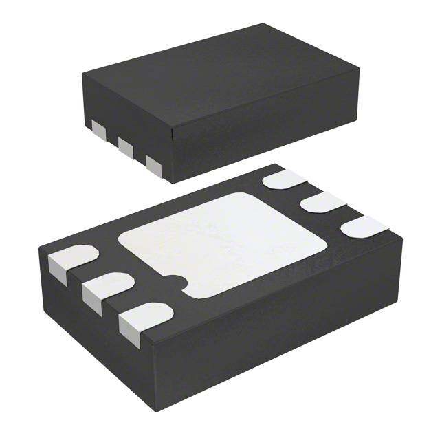
| 描述 | IC DAC 12BIT VOUT W/REF TSOT23-8 |
| 产品分类 | |
| 品牌 | Linear Technology |
| 数据手册 | http://www.linear.com/docs/26554 |
| 产品图片 |
|
| 产品型号 | LTC2640AITS8-HZ12#TRMPBF |
| rohs | 无铅 / 符合限制有害物质指令(RoHS)规范要求 |
| 产品系列 | - |
| 产品目录页面 | |
| 位数 | 12 |
| 供应商器件封装 | TSOT-23-8 |
| 其它名称 | LTC2640AITS8-HZ12#TRMPBFDKR |
| 包装 | Digi-Reel® |
| 安装类型 | 表面贴装 |
| 封装/外壳 | SOT-23-8 薄型,TSOT-23-8 |
| 工作温度 | -40°C ~ 85°C |
| 建立时间 | 4.1µs |
| 数据接口 | 串行 |
| 标准包装 | 1 |
| 电压源 | 单电源 |
| 转换器数 | 1 |
| 输出数和类型 | 1 电压 |
| 配用 | /product-detail/zh/DC1333A-D/DC1333A-D-ND/3029468/product-detail/zh/DC1333A-C/DC1333A-C-ND/3029467/product-detail/zh/DC1333A-B/DC1333A-B-ND/3029466/product-detail/zh/DC1333A-A/DC1333A-A-ND/3029465 |
| 采样率(每秒) | - |


- 商务部:美国ITC正式对集成电路等产品启动337调查
- 曝三星4nm工艺存在良率问题 高通将骁龙8 Gen1或转产台积电
- 太阳诱电将投资9.5亿元在常州建新厂生产MLCC 预计2023年完工
- 英特尔发布欧洲新工厂建设计划 深化IDM 2.0 战略
- 台积电先进制程称霸业界 有大客户加持明年业绩稳了
- 达到5530亿美元!SIA预计今年全球半导体销售额将创下新高
- 英特尔拟将自动驾驶子公司Mobileye上市 估值或超500亿美元
- 三星加码芯片和SET,合并消费电子和移动部门,撤换高东真等 CEO
- 三星电子宣布重大人事变动 还合并消费电子和移动部门
- 海关总署:前11个月进口集成电路产品价值2.52万亿元 增长14.8%


PDF Datasheet 数据手册内容提取
LTC2640 Single 12-/10-/8-Bit SPI V DACs with OUT 10ppm/°C Reference FEATURES DESCRIPTION n Integrated Precision Reference The LTC®2640 is a family of 12-, 10-, and 8-bit voltage- 2.5V Full-Scale 10ppm/°C (LTC2640-L) output DACs with an integrated, high-accuracy, low-drift 4.096V Full-Scale 10ppm/°C (LTC2640-H) reference in an 8-lead TSOT-23 package. It has a rail-to-rail n Maximum INL Error: 1LSB (LTC2640A-12) output buffer that is guaranteed monotonic. n Bidirectional Reference: Input or 10ppm/°C Output The LTC2640-L has a full-scale output of 2.5V, and operates n Low Noise (0.7mVpp, 0.1Hz to 200kHz) from a single 2.7V to 5.5V supply. The LTC2640-H has a n Guaranteed Monotonic Over Temperature full-scale output of 4.096V, and operates from a 4.5V to n 2.7V to 5.5V Supply Range (LTC2640-L) 5.5V supply. A 10ppm/°C reference output is available at n Low Power Operation: 180µA at 3V the REF pin. n Power Down to 1.8µA Maximum (C and I Grades) n Asynchronous DAC Clear Pin (LTC2640-Z) Each DAC can also operate in External Reference mode, n Power-On Reset to Zero or Mid-Scale options in which a voltage supplied to the REF pin sets the full- n Double-Buffered Data Latches scale output. n Guaranteed Operation from –40°C to 125°C (H-Grade) The LTC2640 DACs use a SPI/MICROWIRE™ compatible n 8-Lead TSOT-23 (ThinSOT™) Package 3-wire serial interface which operates at clock rates up to 50MHz. APPLICATIONS The LTC2640 incorporates a power-on reset circuit. Op- n Mobile Communications tions are available for Reset to Zero-Scale or Reset to n Process Control and Industrial Automation Mid-Scale after power-up. n Automatic Test Equipment L, LT, LTC, LTM, Linear Technology and the Linear logo are registered trademarks and n Portable Equipment ThinSOT is a trademark of Analog Devices, Inc. All other trademarks are the property of their n Automotive respective owners. Protected by U.S. Patents, including 5396245, 5859606, 6891433, 6937178 and 7414561. n Optical Networking BLOCK DIAGRAM (LTC2640-Z) VCC REF Integral Nonlinearity (LTC2640A-LZ12) 1.0 INTERNAL SWITCH VCC = 3V SDI REFERENCE VFS = 2.5V 0.5 CONTROL RESISTOR SCK 24-BIT DECODE LOGIC DIVIDER SB) SHIFT L (L 0 REGISTER N I DACREF –0.5 CS/LD INPUT DAC VOUT DAC REGISTER REGISTER –1.0 0 1024 2048 3072 4095 CODE CLR GND 2640 TA01b 2640 TA01 2640fd 1 For more information www.linear.com/LTC2640
LTC2640 ABSOLUTE MAXIMUM RATINGS (Notes 1, 2) Supply Voltage (V ) ...................................–0.3V to 6V Maximum Junction Temperature ..........................150°C CC CLR, CS/LD, REF_SEL, SCK, SDI .................–0.3V to 6V Storage Temperature Range ..................–65°C to 150°C V , REF .........................–0.3V to Min(V + 0.3V, 6V) Lead Temperature (Soldering, 10 sec) ...................300°C OUT CC Operating Temperature Range LTC2640C ................................................0°C to 70°C LTC2640I .............................................–40°C to 85°C LTC2640H ..........................................–40°C to 125°C PIN CONFIGURATION LTC2640-Z LTC2640-M TOP VIEW TOP VIEW CS/LD 1 8 CLR CS/LD 1 8 REF_SEL SCK 2 7 VOUT SCK 2 7 VOUT SDI 3 6 REF SDI 3 6 REF GND 4 5 VCC GND 4 5 VCC TS8 PACKAGE TS8 PACKAGE 8-LEAD PLASTIC TSOT-23 8-LEAD PLASTIC TSOT-23 TJMAX = 150°C (NOTE 5), θJA = 195°C/W TJMAX = 150°C (NOTE 5), θJA = 195°C/W 2640fd 2 For more information www.linear.com/LTC2640
LTC2640 ORDER INFORMATION http://www.linear.com/product/LTC2640#orderinfo LTC2640 A C TS8 –L M 12 #TRM PBF LEAD FREE DESIGNATOR TAPE AND REEL TR = 2,500-Piece Tape and Reel TRM = 500-Piece Tape and Reel RESOLUTION 12 = 12-Bit 10 = 10-Bit 8 = 8-Bit POWER-ON RESET M = Reset to Mid-Scale Z = Reset to Zero-Scale FULL-SCALE VOLTAGE, INTERNAL REFERENCE MODE L = 2.5V H = 4.096V PACKAGE TYPE TS8 = 8-Lead Plastic TSOT-23 TEMPERATURE GRADE C = Commercial Temperature Range (0°C to 70°C) I = Industrial Temperature Range (–40°C to 85°C) H = Automotive Temperature Range (–40°C to 125°C) ELECTRICAL GRADE (OPTIONAL) A = ±1LSB Maximum INL (12-Bit) PRODUCT PART NUMBER Consult LTC Marketing for information on non-standard lead based finish parts. For more information on lead free part marking, go to: http://www.linear.com/leadfree/ For more information on tape and reel specifications, go to: http://www.linear.com/tapeandreel/. Some packages are available in 500 unit reels through designated sales channels with #TRMPBF suffix. 2640fd 3 For more information www.linear.com/LTC2640
LTC2640 PRODUCT SELECTION GUIDE V WITH INTERNAL POWER-ON RESET FS PART NUMBER PART MARKING* REFERENCE TO CODE PIN 8 RESOLUTION V MAXIMUM INL CC LTC2640A-LM12 LTDHV 2.5V • (4095/4096) Mid-Scale REF_SEL 12-Bit 2.7V – 5.5V ±1LSB LTC2640A-LZ12 LTDHW 2.5V • (4095/4096) Zero CLR 12-Bit 2.7V – 5.5V ±1LSB LTC2640A-HM12 LTDHX 4.096V • (4095/4096) Mid-Scale REF_SEL 12-Bit 4.5V – 5.5V ±1LSB LTC2640A-HZ12 LTDHY 4.096V • (4095/4096) Zero CLR 12-Bit 4.5V – 5.5V ±1LSB LTC2640-LM12 LTDHV 2.5V • (4095/4096) Mid-Scale REF_SEL 12-Bit 2.7V – 5.5V ±2.5LSB LTC2640-LM10 LTDHZ 2.5V • (1023/1024) Mid-Scale REF_SEL 10-Bit 2.7V – 5.5V ±1LSB LTC2640-LM8 LTDJF 2.5V • (255/256) Mid-Scale REF_SEL 8-Bit 2.7V – 5.5V ±0.5LSB LTC2640-LZ12 LTDHW 2.5V • (4095/4096) Zero CLR 12-Bit 2.7V – 5.5V ±2.5LSB LTC2640-LZ10 LTDJB 2.5V • (1023/1024) Zero CLR 10-Bit 2.7V – 5.5V ±1LSB LTC2640-LZ8 LTDJG 2.5V • (255/256) Zero CLR 8-Bit 2.7V – 5.5V ±0.5LSB LTC2640-HM12 LTDHX 4.096V • (4095/4096) Mid-Scale REF_SEL 12-Bit 4.5V – 5.5V ±2.5LSB LTC2640-HM10 LTDJC 4.096V • (1023/1024) Mid-Scale REF_SEL 10-Bit 4.5V – 5.5V ±1LSB LTC2640-HM8 LTDJH 4.096V • (255/256) Mid-Scale REF_SEL 8-Bit 4.5V – 5.5V ±0.5LSB LTC2640-HZ12 LTDHY 4.096V • (4095/4096) Zero CLR 12-Bit 4.5V – 5.5V ±2.5LSB LTC2640-HZ10 LTDJD 4.096V • (1023/1024) Zero CLR 10-Bit 4.5V – 5.5V ±1LSB LTC2640-HZ8 LTDJJ 4.096V • (255/256) Zero CLR 8-Bit 4.5V – 5.5V ±0.5LSB *The temperature grade is identified by a label on the shipping container. 2640fd 4 For more information www.linear.com/LTC2640
LTC2640 ELECTRICAL CHARACTERISTICS The l denotes the specifications which apply over the full operating temperature range, otherwise specifications are at T = 25°C. V = 2.7V to 5.5V, V unloaded unless otherwise specified. A CC OUT LTC2640-LM12/-LM10/-LM8/-LZ12/-LZ10/-LZ8, LTC2640A-LM12/-LZ12 (V = 2.5V) FS LTC2640-8 LTC2640-10 LTC2640-12 LTC2640A-12 SYMBOL PARAMETER CONDITIONS MIN TYP MAX MIN TYP MAX MIN TYP MAX MIN TYP MAX UNITS DC Performance Resolution l 8 10 12 12 Bits Monotonicity V = 3V, Internal Ref. (Note 3) l 8 10 12 12 Bits CC DNL Differential V = 3V, Internal Ref. (Note 3) l ±0.5 ±0.5 ±1 ±1 LSB CC Nonlinearity INL Integral V = 3V, Internal Ref. (Note 3) l ±0.05 ±0.5 ±0.2 ±1 ±1 ±2.5 ±0.5 ±1 LSB CC Nonlinearity ZSE Zero-Scale Error V = 3V, Internal Ref., l 0.5 5 0.5 5 0.5 5 0.5 5 mV CC Code = 0 V Offset Error V = 3V, Internal Ref. (Note 4) l ±0.5 ±5 ±0.5 ±5 ±0.5 ±5 ±0.5 ±5 mV OS CC V V Temperature V = 3V, Internal Ref. (Note 4) ±10 ±10 ±10 ±10 µV/°C OSTC OS CC Coefficient FSE Full-Scale Error V = 3V, Internal Ref. (Note 10) l ±0.08 ±0.4 ±0.08 ±0.4 ±0.08 ±0.4 ±0.08 ±0.4 %FSR CC V Full-Scale Voltage V = 3V, Internal Ref. (Note 9) FSTC CC Temperature C-Grade ±10 ±10 ±10 ±10 ppm/°C Coefficient I-Grade ±10 ±10 ±10 ±10 ppm/°C H-Grade ±10 ±10 ±10 ±10 ppm/°C Load Regulation Internal Ref., Mid-Scale, V = 3V ±10%, l 0.009 0.016 0.035 0.064 0.14 0.256 0.14 0.256 LSB/mA CC –5mA ≤ I ≤ 5mA, OUT V = 5V ±10%, l 0.009 0.016 0.035 0.064 0.14 0.256 0.14 0.256 LSB/mA CC –10mA ≤ I ≤ 10mA OUT R DC Output Internal Ref., Mid-Scale, OUT Impedance V = 3V ±10%, l 0.09 0.156 0.09 0.156 0.09 0.156 0.09 0.156 Ω CC –5mA ≤ I ≤ 5mA, OUT V = 5V ±10%, l 0.09 0.156 0.09 0.156 0.09 0.156 0.09 0.156 Ω CC –10mA ≤ I ≤ 10mA OUT SYMBOL PARAMETER CONDITIONS MIN TYP MAX UNITS V DAC Output Span External Reference 0 to V V OUT REF Internal Reference 0 to 2.5 V PSR Power Supply Rejection V = 3V ±10% or 5V ±10% –80 dB CC I Short-Circuit Output Current (Note 5) V = V = 5.5V SC FS CC Sinking Zero-Scale; V shorted to V l 27 48 mA OUT CC Sourcing Full-Scale; V shorted to GND l –28 –48 mA OUT Power Supply V Positive Supply Voltage For Specified Performance l 2.7 5.5 V CC I Supply Current (Note 6) V = 3V, V = 2.5V, External Reference l 150 200 µA CC CC REF V = 3V, Internal Reference l 180 240 µA CC V = 5V, V = 2.5V, External Reference l 160 210 µA CC REF V = 5V, Internal Reference l 190 260 µA CC I Supply Current in Power-Down Mode V = 5V, C-Grade, I-Grade l 0.6 1.8 µA SD CC (Note 6) V = 5V, H-Grade l 0.6 4 µA CC 2640fd 5 For more information www.linear.com/LTC2640
LTC2640 ELECTRICAL CHARACTERISTICS The l denotes the specifications which apply over the full operating temperature range, otherwise specifications are at T = 25°C. V = 2.7V to 5.5V, V unloaded unless otherwise specified. A CC OUT LTC2640-LM12/-LM10/-LM8/-LZ12/-LZ10/-LZ8, LTC2640A-LM12/-LZ12 (V = 2.5V) FS SYMBOL PARAMETER CONDITIONS MIN TYP MAX UNITS Reference Input Input Voltage Range l 0 V V CC Resistance l 160 190 220 kΩ Capacitance 7.5 pF I Reference Current, Power-Down Mode DAC Powered Down l 0.005 0.1 µA REF Reference Output Output Voltage l 1.240 1.250 1.260 V Reference Temperature Coefficient ±10 ppm/°C Output Impedance 0.5 kΩ Capacitive Load Driving 10 µF Short-Circuit Current V = 5.5V; REF Shorted to GND 2.5 mA CC Digital I/O V Digital Input High Voltage V = 3.6V to 5.5V l 2.4 V IH CC V = 2.7V to 3.6V l 2 V CC V Digital Input Low Voltage V = 4.5V to 5.5V l 0.8 V IL CC V = 2.7V to 4.5V l 0.6 V CC I Digital Input Leakage V = GND to V l ±1 µA LK IN CC C Digital Input Capacitance (Note 7) l 2.5 pF IN AC Performance t Settling Time V = 3V (Note 8) S CC ±0.39% (±1LSB at 8-Bits) 3.2 µs ±0.098% (±1LSB at 10-Bits) 3.8 µs ±0.024% (±1LSB at 12-Bits) 4.1 µs Voltage Output Slew Rate 1 V/µs Capacitance Load Driving 500 pF Glitch Impulse At Mid-Scale Transition 2.1 nV•s Multiplying Bandwidth External Reference 300 kHz e Output Voltage Noise Density At f = 1kHz, External Reference 140 nV√Hz n At f = 10kHz, External Reference 130 nV√Hz At f = 1kHz, Internal Reference 160 nV√Hz At f = 10kHz, Internal Reference 150 nV√Hz Output Voltage Noise 0.1Hz to 10Hz, External Reference 20 µV P-P 0.1Hz to 10Hz, Internal Reference 20 µV P-P 0.1Hz to 200kHz, External Reference 650 µV P-P 0.1Hz to 200kHz, Internal Reference, 670 µV P-P C = 0.33µF REF 2640fd 6 For more information www.linear.com/LTC2640
LTC2640 TIMING CHARACTERISTICS The l denotes the specifications which apply over the full operating temperature range, otherwise specifications are at T = 25°C. V = 2.7V to 5.5V. (See Figure 1) (Note 7). A CC LTC2640-LM12/-LM10/-LM8/-LZ12/-LZ10/-LZ8, LTC2640A-LM12/-LZ12 (V = 2.5V) FS SYMBOL PARAMETER CONDITIONS MIN TYP MAX UNITS t SDI Valid to SCK Setup l 4 ns 1 t SDI Valid to SCK Hold l 4 ns 2 t SCK High Time l 9 ns 3 t SCK Low Time l 9 ns 4 t CS/LD Pulse Width l 10 ns 5 t LSB SCK High to CS/LD High l 7 ns 6 t CS/LD Low to SCK High l 7 ns 7 t CLR Pulse Width l 20 ns 9 t CS/LD High to SCK Pos. Edge l 7 ns 10 SCK Frequency 50% Duty Cycle l 50 MHz ELECTRICAL CHARACTERISTICS The l denotes the specifications which apply over the full operating temperature range, otherwise specifications are at T = 25°C. V = 4.5V to 5.5V, V unloaded unless otherwise specified. A CC OUT LTC2640-HM12/-HM10/-HM8/-HZ12/-HZ10/-HZ8, LTC2640A-HM12/-HZ12 (V = 4.096V) FS LTC2640-8 LTC2640-10 LTC2640-12 LTC2640A-12 SYMBOL PARAMETER CONDITIONS MIN TYP MAX MIN TYP MAX MIN TYP MAX MIN TYP MAX UNITS DC Performance Resolution l 8 10 12 12 Bits Monotonicity V = 5V, Internal Ref. (Note 3) l 8 10 12 12 Bits CC DNL Differential V = 5V, Internal Ref. (Note 3) l ±0.5 ±0.5 ±1 ±1 LSB CC Nonlinearity INL Integral V = 5V, Internal Ref. (Note 3) l ±0.05 ±0.5 ±0.2 ±1 ±1 ±2.5 ±0.5 ±1 LSB CC Nonlinearity ZSE Zero-Scale Error V = 5V, Internal Ref., l 0.5 5 0.5 5 0.5 5 0.5 5 mV CC Code = 0 V Offset Error V = 5V, Internal Ref. (Note 4) l ±0.5 ±5 ±0.5 ±5 ±0.5 ±5 ±0.5 ±5 mV OS CC V V Temperature V = 5V, Internal Ref. (Note 4) ±10 ±10 ±10 ±10 µV/°C OSTC OS CC Coefficient FSE Full-Scale Error V = 5V, Internal Ref. (Note 10) l ±0.08 ±0.4 ±0.08 ±0.4 ±0.08 ±0.4 ±0.08 ±0.4 %FSR CC V Full-Scale Voltage V = 5V, Internal Ref. (Note 9) FSTC CC Temperature C-Grade ±10 ±10 ±10 ±10 ppm/°C Coefficient I-Grade ±10 ±10 ±10 ±10 ppm/°C H-Grade ±10 ±10 ±10 ±10 ppm/°C Load Regulation V = 5V ±10%, l 0.006 0.01 0.022 0.04 0.09 0.16 0.09 0.16 LSB/mA CC Internal Ref. Mid-Scale, –10mA ≤ I ≤ 10mA OUT R DC Output V = 5V ±10%, l 0.09 0.156 0.09 0.156 0.09 0.156 0.09 0.156 Ω OUT CC Impedance Internal Ref. Mid-Scale, –10mA ≤ I ≤ 10mA OUT 2640fd 7 For more information www.linear.com/LTC2640
LTC2640 ELECTRICAL CHARACTERISTICS The l denotes the specifications which apply over the full operating temperature range, otherwise specifications are at T = 25°C. V = 4.5V to 5.5V, V unloaded unless otherwise specified. A CC OUT LTC2640-HM12/-HM10/-HM8/-HZ12/-HZ10/-HZ8, LTC2640A-HM12/-HZ12 (V = 4.096V) FS SYMBOL PARAMETER CONDITIONS MIN TYP MAX UNITS V DAC Output Span External Reference 0 to V V OUT REF Internal Reference 0 to 4.096 V PSR Power Supply Rejection V = 5V ±10% –80 dB CC I Short-Circuit Output Current (Note 5) V = V = 5.5V SC FS CC Sinking Zero-Scale; V shorted to V l 27 48 mA OUT CC Sourcing Full-Scale; V shorted to GND l –28 –48 mA OUT Power Supply V Positive Supply Voltage For Specified Performance l 4.5 5.5 V CC I Supply Current (Note 6) V = 5V, V = 4.096V, External Reference l 160 220 µA CC CC REF V = 5V, Internal Reference l 200 270 µA CC I Supply Current in Power-Down Mode V = 5V, C-Grade, I-Grade l 0.6 1.8 µA SD CC (Note 6) V = 5V, H-Grade l 0.6 4 µA CC Reference Input Input Voltage Range l 0 V V CC Resistance l 160 190 220 kΩ Capacitance 7.5 pF I Reference Current, Power-Down DAC Powered Down l 0.005 0.1 µA REF Mode Reference Output Output Voltage l 2.032 2.048 2.064 V Reference Temperature Coefficient ±10 ppm/°C Output Impedance 0.5 kΩ Capacitive Load Driving 10 µF Short-Circuit Current V = 5.5V; REF Shorted to GND 4.3 mA CC Digital I/O V Digital Input High Voltage l 2.4 V IH V Digital Input Low Voltage l 0.8 V IL I Digital Input Leakage V = GND to V l ±1 µA LK IN CC C Digital Input Capacitance (Note 7) l 2.5 pF IN AC Performance t Settling Time V = 5V (Note 8) S CC ±0.39% (±1LSB at 8 Bits) 3.7 µs ±0.098% (±1LSB at 10 Bits) 4.2 µs ±0.024% (±1LSB at 12 Bits) 4.6 µs Voltage Output Slew Rate 1 V/µs Capacitance Load Driving 500 pF Glitch Impulse At Mid-Scale Transition 3.0 nV•s Multiplying Bandwidth External Reference 300 kHz 2640fd 8 For more information www.linear.com/LTC2640
LTC2640 ELECTRICAL CHARACTERISTICS The l denotes the specifications which apply over the full operating temperature range, otherwise specifications are at T = 25°C. V = 4.5V to 5.5V, V unloaded unless otherwise specified. A CC OUT LTC2640-HM12/-HM10/-HM8/-HZ12/-HZ10/-HZ8, LTC2640A-HM12/-HZ12 (V = 4.096V) FS SYMBOL PARAMETER CONDITIONS MIN TYP MAX UNITS e Output Voltage Noise Density At f = 1kHz, External Reference 140 nV√Hz n At f = 10kHz, External Reference 130 nV√Hz At f = 1kHz, Internal Reference 210 nV√Hz At f = 10kHz, Internal Reference 200 nV√Hz Output Voltage Noise 0.1Hz to 10Hz, External Reference 20 µV P-P 0.1Hz to 10Hz, Internal Reference 20 µV P-P 0.1Hz to 200kHz, External Reference 650 µV P-P 0.1Hz to 200kHz, Internal Reference, 670 µV P-P C = 0.33µF REF TIMING CHARACTERISTICS The l denotes the specifications which apply over the full operating temperature range, otherwise specifications are at T = 25°C. V = 4.5V to 5.5V. (See Figure 1) (Note 7). A CC LTC2640-HM12/-HM10/-HM8/-HZ12/-HZ10/-HZ8, LTC2640A-HM12/-HZ12 (V = 4.096V) FS SYMBOL PARAMETER CONDITIONS MIN TYP MAX UNITS t SDI Valid to SCK Setup l 4 ns 1 t SDI Valid to SCK Hold l 4 ns 2 t SCK High Time l 9 ns 3 t SCK Low Time l 9 ns 4 t CS/LD Pulse Width l 10 ns 5 t LSB SCK High to CS/LD High l 7 ns 6 t CS/LD Low to SCK High l 7 ns 7 t CLR Pulse Width l 20 ns 9 t CS/LD High to SCK Pos. Edge l 7 ns 10 SCK Frequency 50% Duty Cycle l 50 MHz Note 1: Stresses beyond those listed under Absolute Maximum Ratings Note 5: This IC includes current limiting that is intended to protect the may cause permanent damage to the device. Exposure to any Absolute device during momentary overload conditions. Junction temperature can Maximum Rating condition for extended periods may affect device exceed the rated maximum during current limiting. Continuous operation reliability and lifetime. above the specified maximum operating junction temperature may impair Note 2: All voltages are with respect to GND. device reliability. Note 3: Linearity and monotonicity are defined from code kL to code Note 6: Digital inputs at 0V or VCC. 2N – 1, where N is the resolution and k is given by k = 0.016 • (2N/ V ), Note 7: Guaranteed by design and not production tested. L L FS rounded to the nearest whole code. For VFS = 2.5V and N = 12, kL = 26 Note 8: Internal Reference mode. DAC is stepped 1/4 scale to 3/4 scale and linearity is defined from code 26 to code 4,095. For VFS = 4.096V and 3/4 scale to 1/4 scale. Load is 2k in parallel with 100pF to GND. and N = 12, k = 16 and linearity is defined from code 16 to code 4,095. L Note 9: Temperature coefficient is calculated by dividing the maximum Note 4: Inferred from measurement at code 16 (LTC2640-12), code 4 change in output voltage by the specified temperature range. (LTC2640-10) or code 1 (LTC2640-8), and at full-scale. Note 10: Full-scale error is determined using the reference voltage measured at the REF pin. 2640fd 9 For more information www.linear.com/LTC2640
LTC2640 TYPICAL PERFORMANCE CHARACTERISTICS T = 25°C, unless otherwise noted. A LTC2640-L12 (Internal Reference, V = 2.5V) FS Reference Output Voltage Integral Nonlinearity (INL) Differential Nonlinearity (DNL) vs Temperature 1.0 1.0 1.260 VCC = 3V VCC = 3V VCC = 3V 0.5 0.5 1.255 NL (LSB) 0 NL (LSB) 0 V (V)REF1.250 I D –0.5 –0.5 1.245 –1.0 –1.0 1.240 0 1024 2048 3072 4095 0 1024 2048 3072 4095 –50 –25 0 25 50 75 100 125 150 CODE CODE TEMPERATURE (°C) 2640 G01 2640 G02 2640 G03 Full-Scale Output Voltage INL vs Temperature DNL vs Temperature vs Temperature 1.0 1.0 2.52 VCC = 3V VCC = 3V VCC = 3V 0.5 0.5 V) 2.51 INL (POS) E ( G INL (LSB) 0 INL (NEG) DNL (LSB) 0 DDNNLL ((PNOEGS)) UTPUT VOLTA2.50 O –0.5 –0.5 FS 2.49 –1.0 –1.0 2.48 –50 –25 0 25 50 75 100 125 150 –50 –25 0 25 50 75 100 125 150 –50 –25 0 25 50 75 100 125 150 TEMPERATURE (°C) TEMPERATURE (°C) TEMPERATURE (°C) 2640 G04 2640 G05 2640 G06 Settling to ±1LSB Settling to ±1LSB 3/4 SCALE TO 1/4 SCALE STEP VCC = 3V, VFS = 2.5V RL = 2k, CL = 100pF CS/LD VOUT AVERAGE OF 256 EVENTS 2V/DIV 1LSB/DIV 4.1µs 3.6µs VOUT 1LSB/DIV 1/4 SCALE TO 3/4 SCALE STEP VCC = 3V, VFS = 2.5V CS/LD RL = 2k, CL = 100pF 2V/DIV AVERAGE OF 256 EVENTS 2µs/DIV 2µs/DIV 2640 G08 2640 G07 2640fd 10 For more information www.linear.com/LTC2640
LTC2640 TYPICAL PERFORMANCE CHARACTERISTICS T = 25°C, unless otherwise noted. A LTC2640-H12 (Internal Reference, V = 4.096V) FS Reference Output Voltage Integral Nonlinearity (INL) Differential Nonlinearity (DNL) vs Temperature 1.0 1.0 2.068 VCC = 5V VCC = 5V VCC = 5V 0.5 0.5 2.058 INL (LSB) 0 DNL (LSB) 0 V (V)REF2.048 –0.5 –0.5 2.038 –1.0 –1.0 2.028 0 1024 2048 3072 4095 0 1024 2048 3072 4095 –50 –25 0 25 50 75 100 125 150 CODE CODE TEMPERATURE (°C) 2640 G09 2640 G10 2640 G11 Full-Scale Output Voltage INL vs Temperature DNL vs Temperature vs Temperature 1.0 1.0 4.115 VCC = 5V VCC = 5V VCC = 5V 0.5 0.5 V)4.105 INL (POS) E ( INL (LSB) 0 INL (NEG) DNL (LSB) 0 DDNNLL ((PNOEGS)) UTPUT VOLTAG4.095 O –0.5 –0.5 FS 4.085 –1.0 –1.0 4.075 –50 –25 0 25 50 75 100 125 150 –50 –25 0 25 50 75 100 125 150 –50 –25 0 25 50 75 100 125 150 TEMPERATURE (°C) TEMPERATURE (°C) TEMPERATURE (°C) 2640 G12 2640 G13 2640 G14 Settling to ±1LSB Settling to ±1LSB CS/LD 5V/DIV VOUT 1LSB/DIV 4.6µs 3.9µs VOUT 1LSB/DIV 1/4 SCALE TO 3/4 SCALE STEP 3/4 SCALE TO 1/4 SCALE STEP VCC = 5V, VFS = 4.095V CS/LD VCC = 5V, VFS = 4.095V RL = 2k, CL = 100pF 5V/DIV RL = 2k, CL = 100pF AVERAGE OF 256 EVENTS AVERAGE OF 256 EVENTS 2µs/DIV 2µs/DIV 2640 G16 2640 G15 2640fd 11 For more information www.linear.com/LTC2640
LTC2640 TYPICAL PERFORMANCE CHARACTERISTICS T = 25°C, unless otherwise noted. A LTC2640-10 Integral Nonlinearity (INL) Differential Nonlinearity (DNL) 1.0 1.0 VCC = 5V VCC = 5V VFS = 4.096V VFS = 4.096V INTERNAL REF. INTERNAL REF. 0.5 0.5 B) B) S S NL (L 0 NL (L 0 I D –0.5 –0.5 –1.0 –1.0 0 256 512 768 1023 0 256 512 768 1023 CODE CODE 2640 G17 2640 G18 LTC2640-8 Integral Nonlinearity (INL) Differential Nonlinearity (DNL) 1.0 0.50 VCC = 3V VCC = 3V VFS = 2.5V VFS = 2.5V INTERNAL REF. INTERNAL REF. 0.5 0.25 INL (LSB) 0 DNL (LSB) 0 –0.5 –0.25 –1.0 –0.50 0 64 128 192 255 0 64 128 192 255 CODE CODE 2640 G19 2640 G20 LTC2640 Load Regulation Current Limiting Offset Error vs Temperature 10 0.20 3 VCC = 5V (LTC2640-H) VCC = 5V (LTC2640-H) 8 VCC = 5V (LTC2640-L) 0.15 VCC = 5V (LTC2640-L) 6 VCC = 3V (LTC2640-L) VCC = 3V (LTC2640-L) 2 0.10 4 V) m 1 V (mV)ΔOUT –202 V(V)∆OUT –00..00505 SET ERROR ( 0 –4 OFF –1 –0.10 –6 –2 –8 INTERNAL REF. –0.15 INTERNAL REF. CODE = MIDSCALE CODE = MIDSCALE –10 –0.20 –3 –30 –20 –10 0 10 20 30 –30 –20 –10 0 10 20 30 –50 –25 0 25 50 75 100 125 150 IOUT (mA) IOUT (mA) TEMPERATURE (°C) 2630 G21 2630 G22 2640 G23 2640fd 12 For more information www.linear.com/LTC2640
LTC2640 TYPICAL PERFORMANCE CHARACTERISTICS T = 25°C, unless otherwise noted. A LTC2640 Gain Error vs V Gain Error vs Temperature Large-Signal Response CC 0.4 0.4 EXTERNAL REF. EXTERNAL REF. 0.3 VREF = 2.5V 0.3 VREF = 2.5V 0.2 0.2 R) R) S S %F 0.1 %F 0.1 R ( R ( RO 0.0 RO 0.0 VOUT R R 0.5V/DIV E E N –0.1 N –0.1 AI AI G G –0.2 –0.2 –0.3 –0.3 VFS = VCC = 5V 1/4 SCALE TO 3/4 SCALE –0.4 –0.4 2.5 3 3.5 4 4.5 5 5.5 –50 –25 0 25 50 75 100 125 150 2µs/DIV VCC (V) TEMPERATURE (°C) 2640 G26 2640 G24 2640 G25 Headroom at Rails Mid-Scale-Glitch Impulse Power-On Reset Glitch vs Output Current 5.0 LTC2640-L 5V SOURCING 4.5 4.0 CS/LD 2V/VDCIVC 3.5 5V/DIV 3V (LTC2640-L) SOURCING 3.0 V) LTC2640-H12, VCC = 5V: (UT 2.5 3.0nV-s TYP O V 2.0 VOUT ZERO-SCALE 1.5 5mV/DIV VOUT 1.0 5V SINKING LTC2640-L12, VCC = 3V: 2mV/DIV 2.1nV-s TYP 0.5 3V (LTC2640-L) SINKING 0 2µs/DIV 200µs/DIV 0 1 2 3 4 5 6 7 8 9 10 2640 G27 2640 G28 IOUT (mA) 2640 G29 Exiting Power-Down to Mid-Scale Supply Current vs Logic Voltage Hardware CLR 1.4 SWEEP SCK, SDI, CS/LD AND CLR BETWEEN CS/LD 1.2 0V AND VCC 2V/DIV 1.0 VOUT 1V/DIV A) 0.8 m VOUT I (CC 0.6 VCC = 5V 0.5V/DIV 0.4 VCC = 3V (LTC2640-L) CLR 0.2 5V/DIV LTC2640-H LTC2640-LZ 0.0 4µs/DIV 0 1 2 3 4 5 1µs/DIV 2640 G30 LOGIC VOLTAGE (V) 2640 G32 2640 G31 2640fd 13 For more information www.linear.com/LTC2640
LTC2640 TYPICAL PERFORMANCE CHARACTERISTICS T = 25°C, unless otherwise noted. A LTC2640 Multiplying Bandwidth Noise Voltage vs Frequency 0.1Hz to 10Hz Voltage Noise 0 500 INTERNAL REF. LTC2640-L, VCC = 4V –2 CODE = MIDSCALE INTERNAL REF. CODE = MIDSCALE –4 400 Hz) –6 V/√ –8 E (n 300 dB–10 VOLTAG 200 L(TVCC2C 6=4 50V-H) 10µV/DIV –12 SE OI –14 VCC = 5V N 100 LTC2640-L VREF(DC) = 2V (VCC = 4V) –16 VREF(AC) = 0.2VP-P CODE = FULL SCALE –18 0 1k 10k 100k 1000k 100 1k 10k 100k 1M 1s/DIV FREQUENCY (Hz) FREQUENCY (Hz) 2640 G35 2640 G33 2640 G34 PIN FUNCTIONS CS/LD (Pin 1): Serial Interface Chip Select/Load Input. full-scale voltage. When Internal Reference is selected, When CS/LD is low, SCK is enabled for shifting data on the 10ppm/°C 1.25V (LTC2640-L) or 2.048V (LTC2640-H) SDI into the register. When CS/LD is taken high, SCK internal reference is available at the pin. This output may is disabled and the specified command (see Table 1) is be bypassed to GND with up to 10µF (0.33µF is recom- executed. mended), and must be buffered when driving external DC load current. SCK (Pin 2): Serial Interface Clock Input. CMOS and TTL compatible. V (Pin 7): DAC Analog Voltage Output. OUT SDI (Pin 3): Serial Interface Data Input. Data on SDI CLR (Pin 8, LTC2640-Z): Asynchronous Clear Input. A is clocked into the DAC on the rising edge of SCK. The logic low at this level-triggered input clears all registers LTC2640 accepts input word lengths of either 24- or 32-bits. and causes the DAC voltage output to reset to Zero. CMOS and TTL compatible. GND (Pin 4): Ground. REF_SEL (Pin 8, LTC2640-M): Selects default Reference V (Pin 5): Supply Voltage Input. 2.7V ≤ V ≤ 5.5V CC CC at power-up. Tie to V to select the Internal Reference, (LTC2640-L) or 4.5V ≤ V ≤ 5.5V (LTC2640-H). Bypass CC CC or GND to select an External Reference. After power-up, to GND with a 0.1µF capacitor. the logic state at this pin is ignored and the reference may REF (Pin 6): Reference Voltage Input or Output. When be changed only by software command. External Reference mode is selected, REF is an input (0V ≤ V ≤ V ) where the voltage supplied sets the REF CC 2640fd 14 For more information www.linear.com/LTC2640
LTC2640 BLOCK DIAGRAMS LTC2640-Z VCC REF INTERNAL REFERENCE SWITCH SDI CONTROL RESISTOR DECODE LOGIC DIVIDER SCK 24-BIT SHIFT REGISTER DACREF CS/LD INPUT DAC VOUT DAC REGISTER REGISTER CLR GND LTC2640-M VCC REF INTERNAL REF_SEL REFERENCE SWITCH SDI CONTROL DECODE LOGIC RESISTOR SCK 24-BIT DIVIDER SHIFT REGISTER DACREF CS/LD INPUT DAC VOUT DAC REGISTER REGISTER GND 2640 BD 2640fd 15 For more information www.linear.com/LTC2640
LTC2640 TIMING DIAGRAM t1 t2 t3 t4 t6 SCK 1 2 3 23 24 t10 SDI t5 t7 CS/LD 2640 F01 Figure 1. Serial Interface Timing 2640fd 16 For more information www.linear.com/LTC2640
LTC2640 OPERATION The LTC2640 is a family of single voltage-output DACs The LTC2640-HM/LTC2640-LM provide an alternative in 8-lead ThinSOT packages. Each DAC can operate rail- reset, setting the output to mid-scale when power is first to-rail using an external reference, or with its full-scale applied. voltage set by an integrated reference. 12 combinations of Default reference mode selection is described in the Refer- accuracy (12-, 10-, and 8-bit), power-on reset value (zero ence Modes section. or mid-scale), and full-scale voltage (2.5V or 4.096V) are available. The LTC2640 is controlled using a 3-wire SPI/ Power Supply Sequencing MICROWIRE compatible interface. The voltage at REF (Pin 6) should be kept within the range Power-On Reset –0.3V ≤ VREF ≤ VCC + 0.3V (see Absolute Maximum Rat- ings). Particular care should be taken to observe these The LTC2640-HZ/LTC2640-LZ clear the output to zero- limits during power supply turn-on and turn-off sequences, scale when power is first applied, making system initializa- when the voltage at V (Pin 5) is in transition. CC tion consistent and repeatable. For some applications, downstream circuits are active Transfer Function during DAC power-up, and may be sensitive to nonzero The digital-to-analog transfer function is: outputs from the DAC during this time. The LTC2640 contains circuitry to reduce the power-on glitch: the k analog output typically rises less than 5mV above zero- VOUT(IDEAL)=2NVREF scale during power on if the power supply is ramped where k is the decimal equivalent of the binary DAC input to 5V in 1ms or more. In general, the glitch amplitude code, N is the resolution, and V is either 2.5V (LTC2640- decreases as the power supply ramp time is increased. REF LM/LTC2640-LZ) or 4.096V (LTC2640-HM/LTC2640-HZ) See “Power-On Reset Glitch” in the Typical Performance when in Internal Reference mode, and the voltage at REF Characteristics section. (Pin 6) when in External Reference mode. INPUT WORD (LTC2640-12) COMMAND 4 DON'T-CARE BITS DATA (12 BITS + 4 DON'T-CARE BITS) C3 C2 C1 C0 X X X X D11 D10 D9 D8 D7 D6 D5 D4 D3 D2 D1 D0 X X X X MSB LSB INPUT WORD (LTC2640-10) COMMAND 4 DON'T-CARE BITS DATA (10 BITS + 6 DON'T-CARE BITS) C3 C2 C1 C0 X X X X D9 D8 D7 D6 D5 D4 D3 D2 D1 D0 X X X X X X MSB LSB INPUT WORD (LTC2640-8) COMMAND 4 DON'T-CARE BITS DATA (8 BITS + 8 DON'T-CARE BITS) C3 C2 C1 C0 X X X X D7 D6 D5 D4 D3 D2 D1 D0 X X X X X X X X MSB LSB 2640 F02 Figure 2. Command and Data Input Format 2640fd 17 For more information www.linear.com/LTC2640
LTC2640 OPERATION Serial Interface transferred to the device first, followed by the 24-bit se- quence described. Figure 3b shows the 32-bit sequence. The CS/LD input is level triggered. When this input is taken low, it acts as a chip-select signal, enabling the The 16-bit data word is ignored for all commands that do SDI and SCK buffers and the input shift register. Data not include a Write operation. (SDI input) is transferred at the next 24 rising SCK edges. The 4-bit command, C3-C0, is loaded first, followed by Reference Modes 4 don’t-cares bits, and finally the 16-bit data word. The For applications where an accurate external reference is not data word comprises the 12-, 10- or 8-bit input code, or- available, the LTC2640 has a user-selectable, integrated dered MSB-to-LSB, followed by 4, 6 or 8 don’t-cares bits reference. The LTC2640-LM/LTC2640-LZ provide a full- (LTC2640-12, LTC2640-10 and LTC2640-8 respectively; scale output of 2.5V. The LTC2640-HM/LTC2640-HZ see Figure 2). Data can only be transferred to the device provide a full-scale output of 4.096V. The internal reference when the CS/LD signal is low, beginning on the first rising can be useful in applications where the supply voltage is edge of SCK. SCK may be high or low at the falling edge poorly regulated. Internal Reference mode can be selected of CS/LD. The rising edge of CS/LD ends the data transfer by using command 0110, and is the power-on default for and causes the device to execute the command specified LTC2640-HZ/LTC2640-LZ, as well as for LTC2640-HM/ in the 24-bit input sequence. The complete sequence is LTC2640-LM when REF_SEL is tied high. shown in Figure 3a. The 10ppm/°C, 1.25V (LTC2640-LM/LTC2640-LZ) or The command (C3-C0) assignments are shown in Table 1. 2.048V (LTC2640-HM/LTC2640-HZ) internal reference The first three commands in the table consist of write and is available at the REF pin. Adding bypass capacitance update operations. A Write operation loads a 16-bit data to the REF pin will improve noise performance; 0.33µF word from the 24-bit shift register into the input register. is recommended, and up to 10µF can be driven without In an Update operation, the input register is copied to the oscillation. This output must be buffered when driving an DAC register and converted to an analog voltage at the external DC load current. DAC output. Write to and Update combines the first two Alternatively, the DAC can operate in External Reference commands. The Update operation also powers up the mode using command 0111. In this mode, an input voltage DAC if it had been in power-down mode. The data path supplied externally to the REF pin provides the reference and registers are shown in the Block Diagram. (0V ≤ V ≤ V ) and the supply current is reduced. External REF CC Table 1. Command Codes Reference mode is the power-on default for LTC2640-HM/ COMMAND* LTC2640-LM when REF_SEL is tied low. C3 C2 C1 C0 The reference mode of LTC2640-HZ/LTC2640-LZ can be 0 0 0 0 Write to Input Register changed only by software command. The same is true for 0 0 0 1 Update (Power-Up) DAC Register LTC2640-HM/LTC2640-LM after power-on, after which 0 0 1 1 Write to and Update (Power-Up) DAC Register the logic state on REF_SEL is ignored. 0 1 0 0 Power Down 0 1 1 0 Select Internal Reference Power-Down Mode 0 1 1 1 Select External Reference For power-constrained applications, the LTC2640’s power- *Command codes not shown are reserved and should not be used down mode can be used to reduce the supply current While the minimum input sequence is 24-bits, it may whenever the DAC output is not needed. When in power- optionally be extended to 32-bits to accommodate micro- down, the buffer amplifier, bias circuit, and reference processors that have a minimum word width of 16-bits circuit are disabled and draw essentially zero current. The (2-bytes). To use the 32-bit width, 8 don’t-cares bits are DAC output is put into a HIGH-impedance state, and the output pin is passively pulled to ground through a 200k 2640fd 18 For more information www.linear.com/LTC2640
LTC2640 OPERATION resistor. Input and DAC register contents are not disturbed Since the analog output of the DAC cannot go below ground, during power-down. it may limit the lowest codes, as shown in Figure 4b. Similarly, limiting can occur near full-scale when the REF The DAC can be put into power-down mode by using pin is tied to V . If V = V and the DAC full-scale error command 0100. The supply current is reduced to 1.8µA CC REF CC (FSE) is positive, the output for the highest codes limits maximum (C and I grades) and the REF pin becomes HIGH at V , as shown in Figure 4c. No full-scale limiting can impedance (typically > 1GΩ). CC occur if V is less than V – FSE. REF CC Normal operation resumes after executing any command Offset and linearity are defined and tested over the region that includes a DAC update, as shown in Table 1. The DAC of the DAC transfer function where no output limiting can is powered up and its voltage output is updated. Normal occur. settling is delayed while the bias, reference, and ampli- fier circuits are re-enabled. When the REF pin output is Board Layout bypassed to GND with 1nF or less, the power-up delay time is 20µs for settling to 12-bits. This delay increases The PC board should have separate areas for the analog and to 200µs for 0.33µF, and 10ms for 10µF. digital sections of the circuit. A single, solid ground plane should be used, with analog and digital signals carefully Voltage Output routed over separate areas of the plane. This keeps digital signals away from sensitive analog signals and minimizes The LTC2640’s integrated rail-to-rail amplifier has guar- the interaction between digital ground currents and the anteed load regulation when sourcing or sinking up to analog section of the ground plane. The resistance from 10mA at 5V, and 5mA at 3V. the LTC2640 GND pin to the ground plane should be as Load regulation is a measure of the amplifier’s ability to low as possible. Resistance here will add directly to the maintain the rated voltage accuracy over a wide range of effective DC output impedance of the device (typically load current. The measured change in output voltage per 0.1Ω). Note that the LTC2640 is no more susceptible to change in forced load current is expressed in LSB/mA. this effect than any other parts of this type; on the con- trary, it allows layout-based performance improvements DC output impedance is equivalent to load regulation, and to shine rather than limiting attainable performance with may be derived from it by simply calculating a change in excessive internal resistance. units from LSB/mA to ohms. The amplifier’s DC output impedance is 0.1Ω when driving a load well away from Another technique for minimizing errors is to use a sepa- the rails. rate power ground return trace on another board layer. The trace should run between the point where the power When drawing a load current from either rail, the output supply is connected to the board and the DAC ground pin. voltage headroom with respect to that rail is limited by Thus the DAC ground pin becomes the common point for the 50Ω typical channel resistance of the output devices analog ground, digital ground, and power ground. When (e.g., when sinking 1mA, the minimum output voltage is the LTC2640 is sinking large currents, this current flows 50Ω • 1mA, or 50mV). See the graph “Headroom at Rails out the ground pin and directly to the power ground trace vs. Output Current” in the Typical Performance Charac- without affecting the analog ground plane voltage. teristics section. It is sometimes necessary to interrupt the ground plane The amplifier is stable driving capacitive loads of up to to confine digital ground currents to the digital portion of 500pF. the plane. When doing this, make the gap in the plane only Rail-to-Rail Output Considerations as long as it needs to be to serve its purpose and ensure that no traces cross over the gap. In any rail-to-rail voltage output device, the output is limited to voltages within the supply range. 2640fd 19 For more information www.linear.com/LTC2640
LTC2640 OPERATION 2640 F03b 2 3 X 1 3 2640 F03a 30 XX 4 2 X 29 X 3 2 X 28 0 D 2 2 X 27 1 D 1 2 X 26 2 D 0 2 D0 25 D3 ORD 9 W 5681591416111810127131417 C0XXXXD11D10D9D8D7D6D5D4D3D2D1 D4 DON’T-CARE BITSDATA WORD 24-BIT INPUT WORD Figure 3a. LTC2640-12 24-Bit Load Sequence (Minimum Input Word).LTC2640-10 SDI Data Word: 10-Bit Input Code + 6 Don’t-Cares Bits;LTC2640-8 SDI Data Word: 8-Bit Input Code + 8 Don’t-Cares Bits 1591916201122182410122123131417 C2C1C0XXXXD11D10D9D8D7D6D5D4C3 4 DON’T-CARE BITSCOMMAND WORDDATA 32-BIT INPUT WORD Figure 3b. LTC2640-12 32-Bit Load SequenceLTC2640-10 SDI Data Word: 10-Bit Input Code + 6 Don’t-Cares Bits;LTC2640-8 SDI Data Word: 8-Bit Input Code + 8 Don’t-Cares Bits R 3 C1 D WO 8 X N 2 C2 MMA 7 X O 1 C3 C 6 X S T 5 X RE BI A CS/LD SCK SDI 4 X ON’T-C D 3 8 X 2 X 1 X S/LD SCK SDI C 2640fd 20 For more information www.linear.com/LTC2640
LTC2640 OPERATION POSITIVE VREF = VCC FSE VREF = VCC OUTPUT VOLTAGE OUTPUT VOLTAGE INPUT CODE 2640 F04 (c) OUTPUT VOLTAGE 0V 0 2,048 4,095 INPUT CODE (a) 0V NEGATIVE INPUT CODE OFFSET (b) Figure 4. Effects of Rail-to-Rail Operation on a DAC Transfer Curve (Shown for 12-Bits) (a) Overall Transfer Function (b) Effect of Negative Offset for Codes Near Zero (c) Effect of Positive Full-Scale Error for Codes Near Full-Scale 2640fd 21 For more information www.linear.com/LTC2640
LTC2640 PACKAGE DESCRIPTION Please refer to http://www.linear.com/product/LTC2640#packaging for the most recent package drawings. TS8 Package 8-Lead Plastic TSOT-23 (Reference LTC DWG # 05-08-1637 Rev A) 2.90 BSC 0.40 0.65 (NOTE 4) MAX REF 1.22 REF 1.50 – 1.75 3.85 MAX2.62 REF 1.4 MIN 2.80 BSC (NOTE 4) PIN ONE ID RECOMMENDED SOLDER PAD LAYOUT 0.22 – 0.36 0.65 BSC PER IPC CALCULATOR 8 PLCS (NOTE 3) 0.80 – 0.90 0.20 BSC 0.01 – 0.10 1.00 MAX DATUM ‘A’ 0.30 – 0.50 REF 1.95 BSC 0.09 – 0.20 TS8 TSOT-23 0710 REV A (NOTE 3) NOTE: 1. DIMENSIONS ARE IN MILLIMETERS 2. DRAWING NOT TO SCALE 3. DIMENSIONS ARE INCLUSIVE OF PLATING 4. DIMENSIONS ARE EXCLUSIVE OF MOLD FLASH AND METAL BURR 5. MOLD FLASH SHALL NOT EXCEED 0.254mm 6. JEDEC PACKAGE REFERENCE IS MO-193 2640fd 22 For more information www.linear.com/LTC2640
LTC2640 REVISION HISTORY (Revision history begins at Rev C) REV DATE DESCRIPTION PAGE NUMBER C 10/13 Updated TS8 package drawing to Rev A. 22 D 06/17 Removed Note 3. 9 2640fd Information furnished by Linear Technology Corporation is believed to be accurate and reliable. 23 However, no responsibility is assumed for its use. Linear Technology Corporation makes no representa- tion that the interconneFcotior nm oof irtse ciinrcfouirtms aast dioensc wribwedw h.leirneeina rw.cilol nmot/ LinTfCrin2g6e4 o0n existing patent rights.
LTC2640 TYPICAL APPLICATION Programmable ±5V Output 5V 5V 5 0.1µF 4 – 0.1µF 1 10V LTC2054 3 + 8 5 6 2 9 MM93 7 0.1µF 8 VCC REF 10 VCC REF_SEL M1 SERBIUASL 32 SSDCKI LT-CL2M61420A VOUT 7 12 PP13 LT1V9E9E1REFO5UT 6 VOUT = ±5V 1 3 P9 4 CS/LD GND 4 0.1µF –10V 2640 TA03 RELATED PARTS PART NUMBER DESCRIPTION COMMENTS LTC1663 Single 10-Bit V DAC in SOT-23 V = 2.7V to 5.5V, 60µA, Internal Reference, SMBus Interface OUT CC LTC1669 Single 10-Bit V DAC in SOT-23 V = 2.7V to 5.5V, 60µA, Internal Reference, I2C Interface OUT CC LTC2360/LTC2362/ 12-Bit SAR ADCs in TSOT23-6/TSOT23-8 Packages 100ksps/250ksps/500ksps/1Msps/3Msps Output Rates LTC2365/LTC2366 LTC2450/LTC2452 16-Bit Single-Ended/Differential Delta Sigma ADCs SPI Interface, Tiny DFN Packages, 60Hz Output Rate LTC2451/LTC2453 16-Bit Single-Ended/Differential Delta Sigma ADCs I2C Interface, Tiny DFN and TSOT23-8 Packages, 60Hz Output Rate LTC2600/LTC2610/LTC2620 Octal 16-/14-/12-Bit V DACs in 16-Lead SSOP 250µA per DAC, 2.5V to 5.5V Supply Range, Rail-to-Rail Output, OUT SPI Serial Interface LTC2601/LTC2611/LTC2621 Single 16-/14-/12-Bit V DACs in 10-Lead DFN 300µA per DAC, 2.5V to 5.5V Supply Range, Rail-to-Rail Output, OUT SPI Serial Interface LTC2602/LTC2612/LTC2622 Dual 16-/14-/12-Bit V DACs in 8-Lead MSOP 300µA per DAC, 2.5V to 5.5V Supply Range, Rail-to-Rail Output, OUT SPI Serial Interface LTC2604/LTC2614/LTC2624 Quad 16-/14-/12-Bit V DACs in 16-Lead SSOP 250µA per DAC, 2.5V to 5.5V Supply Range, Rail-to-Rail Output, OUT SPI Serial Interface LTC2605/LTC2615/LTC2625 Octal 16-/14-/12-Bit V DACs with I2C Interface 250µA per DAC, 2.5V to 5.5V Supply Range, Rail-to-Rail Output, OUT I2C Interface LTC2606/LTC2616/LTC2626 Single 16-/14-/12-Bit V DACs with I2C Interface 270µA per DAC, 2.5V to 5.5V Supply Range, Rail-to-Rail Output, OUT I2C Interface LTC2609/LTC2619/LTC2629 Quad 16-/14-/12-Bit V DACs with I2C Interface 250µA per DAC, 2.5V to 5.5V Supply Range, Rail-to-Rail Output with OUT Separate V Pins for Each DAC REF LTC2630 Single 12-/10-/8-Bit V DACs with 10ppm/°C 180µA per DAC, 2.7V to 5.5V Supply Range, 10ppm/°C Reference, OUT Reference in SC70 Rail-to-Rail Output, SPI Interface LTC2631 Single 12-/10-/8-Bit I2C V DACs with 10ppm/°C 180µA per DAC, 2.7V to 5.5V Supply Range, 10ppm/°C Reference, OUT Reference in ThinSOT Selectable External Ref. Mode, Rail-to-Rail Output, I2C Interface 2640fd 24 LT 0617 REV D • PRINTED IN USA www.linear.com/LTC2640 For more information www.linear.com/LTC2640 LINEAR TECHNOLOGY CORPORATION 2008
Mouser Electronics Authorized Distributor Click to View Pricing, Inventory, Delivery & Lifecycle Information: A nalog Devices Inc.: LTC2640ITS8-LZ8#TRPBF LTC2640ITS8-LM10#TRPBF LTC2640AITS8-LZ12#TRPBF LTC2640HTS8-LZ8#PBF LTC2640CTS8-LZ10#TRPBF LTC2640CTS8-LM10#TRMPBF LTC2640ITS8-LZ10#PBF LTC2640AITS8-LZ12#PBF LTC2640HTS8-LZ10#TRMPBF LTC2640HTS8-LM12#PBF LTC2640CTS8-HZ12#TRPBF LTC2640CTS8-HM8#PBF LTC2640AHTS8-LZ12#TRMPBF LTC2640ITS8-HM12#TRPBF LTC2640ACTS8-LM12#TRPBF LTC2640CTS8- HZ8#PBF LTC2640CTS8-LZ8#TRMPBF LTC2640CTS8-LZ10#PBF LTC2640HTS8-HM10#PBF LTC2640HTS8- HM10#TRPBF LTC2640ITS8-LM8#TRMPBF LTC2640ITS8-LZ10#TRPBF LTC2640CTS8-HM8#TRPBF LTC2640CTS8-LM12#TRPBF LTC2640AITS8-HM12#TRPBF LTC2640AHTS8-LM12#PBF LTC2640HTS8- LZ10#TRPBF LTC2640CTS8-HM12#TRMPBF LTC2640ITS8-HZ10#TRMPBF LTC2640HTS8-HZ10#PBF LTC2640ITS8-LM8#TRPBF LTC2640ITS8-HM8#TRMPBF LTC2640ACTS8-LZ12#PBF LTC2640CTS8-LZ8#TRPBF LTC2640ITS8-HM10#PBF LTC2640ITS8-LM12#TRMPBF LTC2640ACTS8-LM12#PBF LTC2640CTS8-HZ10#PBF LTC2640ACTS8-LZ12#TRMPBF LTC2640CTS8-HM12#TRPBF LTC2640CTS8-LM10#TRPBF LTC2640HTS8- HZ12#TRPBF LTC2640AHTS8-HM12#TRMPBF LTC2640AITS8-LM12#TRMPBF LTC2640CTS8-LM10#PBF LTC2640ITS8-HZ8#TRMPBF LTC2640AHTS8-HZ12#TRPBF LTC2640ITS8-LZ12#TRMPBF LTC2640AHTS8- LZ12#PBF LTC2640ITS8-HM10#TRMPBF LTC2640ACTS8-HZ12#TRMPBF LTC2640HTS8-HM8#TRPBF LTC2640CTS8-HZ10#TRMPBF LTC2640HTS8-HM12#PBF LTC2640HTS8-LM12#TRPBF LTC2640HTS8-HZ12#PBF LTC2640CTS8-HZ10#TRPBF LTC2640AHTS8-HM12#TRPBF LTC2640CTS8-LM8#TRPBF LTC2640ITS8- HZ12#TRMPBF LTC2640ACTS8-HM12#TRMPBF LTC2640CTS8-LM12#TRMPBF LTC2640HTS8-HM12#TRPBF LTC2640ITS8-LZ10#TRMPBF LTC2640AITS8-HZ12#TRMPBF LTC2640AHTS8-HZ12#PBF LTC2640HTS8-HZ8#PBF LTC2640HTS8-HM10#TRMPBF LTC2640ITS8-HZ10#PBF LTC2640HTS8-LM10#TRPBF LTC2640AITS8- HM12#PBF LTC2640ITS8-HZ8#TRPBF LTC2640HTS8-HM8#PBF LTC2640HTS8-LM10#TRMPBF LTC2640ITS8- LM10#PBF LTC2640AITS8-LM12#TRPBF LTC2640ITS8-LZ12#TRPBF LTC2640CTS8-HM10#PBF LTC2640ITS8- HZ12#PBF LTC2640ITS8-LM12#PBF LTC2640ACTS8-HM12#PBF LTC2640HTS8-HM12#TRMPBF LTC2640HTS8- LZ8#TRMPBF LTC2640ITS8-HM10#TRPBF LTC2640HTS8-LM8#TRMPBF LTC2640HTS8-LM10#PBF LTC2640CTS8-HM8#TRMPBF LTC2640AHTS8-LM12#TRMPBF LTC2640CTS8-LZ12#TRMPBF LTC2640HTS8- LZ8#TRPBF LTC2640ACTS8-HM12#TRPBF LTC2640ACTS8-LM12#TRMPBF LTC2640ITS8-HZ8#PBF LTC2640ITS8-LM10#TRMPBF LTC2640CTS8-HZ12#TRMPBF LTC2640CTS8-HZ8#TRMPBF LTC2640CTS8- LZ12#PBF LTC2640CTS8-LM8#PBF LTC2640HTS8-HM8#TRMPBF LTC2640ITS8-HM12#PBF