ICGOO在线商城 > 集成电路(IC) > 数据采集 - 模数转换器 > LTC2263IUJ-12#PBF

 Datasheet下载
- 型号: LTC2263IUJ-12#PBF
- 制造商: LINEAR TECHNOLOGY
- 库位|库存: xxxx|xxxx
- 要求:
| 数量阶梯 | 香港交货 | 国内含税 |
| +xxxx | $xxxx | ¥xxxx |
查看当月历史价格
查看今年历史价格
LTC2263IUJ-12#PBF产品简介:
ICGOO电子元器件商城为您提供LTC2263IUJ-12#PBF由LINEAR TECHNOLOGY设计生产,在icgoo商城现货销售,并且可以通过原厂、代理商等渠道进行代购。 LTC2263IUJ-12#PBF价格参考。LINEAR TECHNOLOGYLTC2263IUJ-12#PBF封装/规格:数据采集 - 模数转换器, 12 Bit Analog to Digital Converter 2 Input 2 Pipelined 40-QFN (6x6)。您可以下载LTC2263IUJ-12#PBF参考资料、Datasheet数据手册功能说明书,资料中有LTC2263IUJ-12#PBF 详细功能的应用电路图电压和使用方法及教程。
LTC2263IUJ-12#PBF 是 Linear Technology(现为 Analog Devices)生产的一款 12 位模数转换器(ADC),属于数据采集系统中的核心组件。以下是其典型应用场景:

 1. 工业自动化与控制
   - 在工业自动化中,LTC2263 可用于数据采集模块,将传感器输出的模拟信号(如温度、压力、振动等)转换为数字信号,供微控制器或处理器分析和处理。
   - 应用实例:工业机器人状态监测、工厂生产线监控系统。

 2. 通信设备
   - 适用于通信领域的信号接收与处理,例如软件定义无线电(SDR)、基站接收机等。
   - 能够将射频或中频信号转换为数字信号,支持高速数据传输和处理。

 3. 医疗设备
   - 在医疗电子领域,该 ADC 可用于心电图(ECG)、脑电图(EEG)、超声波成像等设备中,实现高精度的生理信号采集。
   - 其低噪声特性确保了对微弱生物电信号的准确转换。

 4. 测试与测量仪器
   - 广泛应用于示波器、频谱分析仪和其他测试设备中,用于实时采集和显示信号波形。
   - 提供高分辨率和快速采样能力,满足复杂信号分析需求。

 5. 汽车电子
   - 在汽车行业中,可用于车载雷达、胎压监测系统(TPMS)、发动机控制单元(ECU)等场景。
   - 实现对车辆运行状态的精确监控,提升驾驶安全性和舒适性。

 6. 音频处理
   - 适合高质量音频信号的数字化处理,例如专业音频设备、录音设备等。
   - 提供低失真和高信噪比性能,确保音频质量。

 总结
LTC2263IUJ-12#PBF 凭借其 12 位分辨率、高达 65MSPS 的采样率以及优异的动态性能,适用于需要高精度、高速度数据采集的各种场景。它在工业、通信、医疗、测试测量等领域具有广泛的用途,能够满足多种复杂应用的需求。
| 参数 | 数值 |
| 产品目录 | 集成电路 (IC) |
| 描述 | IC ADC 12BIT SER/PAR 25M 40-QFN |
| 产品分类 | |
| 品牌 | Linear Technology |
| 数据手册 | http://www.linear.com/docs/28910 |
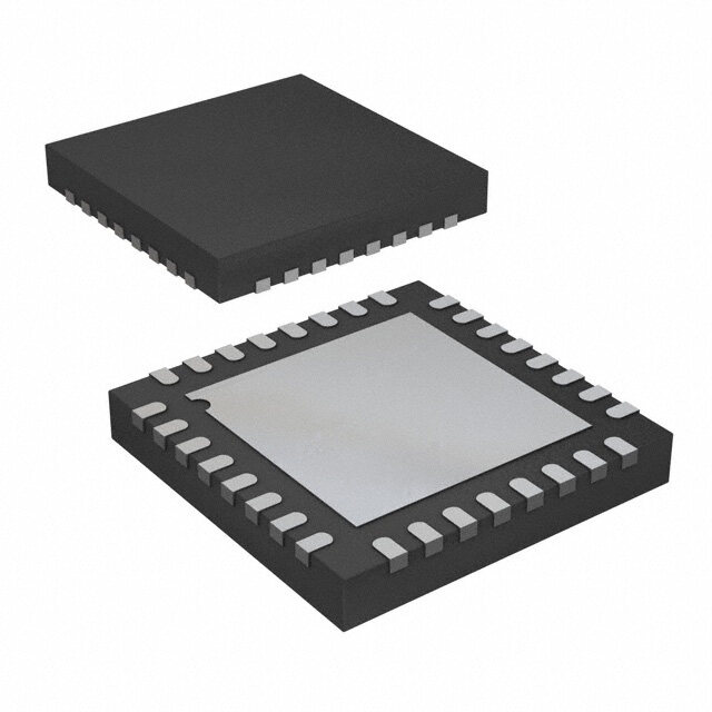
| 产品图片 |
|
| 产品型号 | LTC2263IUJ-12#PBF |
| PCN设计/规格 | |
| rohs | 无铅 / 符合限制有害物质指令(RoHS)规范要求 |
| 产品系列 | - |
| 位数 | 12 |
| 供应商器件封装 | 40-QFN(6x6) |
| 其它名称 | LTC2263IUJ12PBF |
| 包装 | 管件 |
| 安装类型 | 表面贴装 |
| 封装/外壳 | 40-WFQFN 裸露焊盘 |
| 工作温度 | -40°C ~ 85°C |
| 数据接口 | 串行 LVDS |
| 标准包装 | 61 |
| 特性 | 同步采样 |
| 电压源 | 模拟和数字 |
| 转换器数 | 2 |
| 输入数和类型 | 2 个差分; 2 个单端 |
| 配用 | /product-detail/zh/DC1532A-L/DC1532A-L-ND/3025176/product-detail/zh/DC1532A-F/DC1532A-F-ND/3025170 |
| 采样率(每秒) | 25M |


- 商务部:美国ITC正式对集成电路等产品启动337调查
- 曝三星4nm工艺存在良率问题 高通将骁龙8 Gen1或转产台积电
- 太阳诱电将投资9.5亿元在常州建新厂生产MLCC 预计2023年完工
- 英特尔发布欧洲新工厂建设计划 深化IDM 2.0 战略
- 台积电先进制程称霸业界 有大客户加持明年业绩稳了
- 达到5530亿美元!SIA预计今年全球半导体销售额将创下新高
- 英特尔拟将自动驾驶子公司Mobileye上市 估值或超500亿美元
- 三星加码芯片和SET,合并消费电子和移动部门,撤换高东真等 CEO
- 三星电子宣布重大人事变动 还合并消费电子和移动部门
- 海关总署:前11个月进口集成电路产品价值2.52万亿元 增长14.8%


PDF Datasheet 数据手册内容提取
LTC2265-12/ LTC2264-12/LTC2263-12 12-Bit, 65Msps/40Msps/ 25Msps Low Power Dual ADCs FEATURES DESCRIPTION n 2-Channel Simultaneous Sampling ADC The LTC®2265-12/LTC2264-12/LTC2263-12 are 2-channel, n 71dB SNR simultaneous sampling 12-bit A/D converters designed for n 90dB SFDR digitizing high frequency, wide dynamic range signals. They n Low Power: 167mW/112mW/94mW Total are perfect for demanding communications applications n 83mW/56mW/47mW per Channel with AC performance that includes 71dB SNR and 90dB n Single 1.8V Supply spurious free dynamic range (SFDR). Ultralow jitter of n Serial LVDS Outputs: 1 or 2 Bits per Channel 0.15ps allows undersampling of IF frequencies with RMS n Selectable Input Ranges: 1VP-P to 2VP-P excellent noise performance. n 800MHz Full Power Bandwidth S/H DC specs include ±0.3LSB INL (typ), ±0.1LSB DNL (typ) n Shutdown and Nap Modes and no missing codes over temperature. The transition n Serial SPI Port for Configuration noise is a low 0.3LSB . n Pin Compatible 14-Bit and 12-Bit Versions RMS n 40-Pin (6mm × 6mm) QFN Package The digital outputs are serial LVDS to minimize the num- ber of data lines. Each channel outputs two bits at a time (2-lane mode) or one bit at a time (1-lane mode). The LVDS APPLICATIONS drivers have optional internal termination and adjustable output levels to ensure clean signal integrity. n Communications n Cellular Base Stations The ENC+ and ENC– inputs may be driven differentially n Software Defined Radios or single-ended with a sine wave, PECL, LVDS, TTL, or n Portable Medical Imaging CMOS inputs. An internal clock duty cycle stabilizer n Multichannel Data Acquisition allows high performance at full speed for a wide range of n Nondestructive Testing clock duty cycles. L, LT, LTC, LTM, Linear Technology and the Linear logo are registered trademarks of Linear Technology Corporation. All other trademarks are the property of their respective owners. TYPICAL APPLICATION LTC2265-12, 65Msps, 2-Tone FFT, f = 70MHz and 75MHz IN 1.8V 1.8V 0 VDD OVDD –10 CH.1 + 12-BIT OUT1A –20 ANALOG S/H –30 INPUT – ADC CORE OUT1B FS)–40 B ANACLHO.G2 +S/H 12-BIT SERDIAATLAIZER OUT2A SLVEDRSIALIZED UDE (d––6500 INPUT – ADC CORE OUT2B OUTPUTS LIT–70 P DATA AM–80 CLOCK ENCODE –90 PLL OUT INPUT –100 FRAME –110 –120 GND OGND 0 10 20 30 FREQUENCY (MHz) 226512 TA01 226512 TA02 22654312fb 1
LTC2265-12/ LTC2264-12/LTC2263-12 ABSOLUTE MAXIMUM RATINGS PIN CONFIGURATION (Notes 1 and 2) Supply Voltages TOP VIEW AnValDoDg, IOnVpuDDt .V..o..l.t.a..g..e. .(..A..I.N..+..,. .A..I.N..–.,. .P..A...R../.S..E..R...,. –0.3V to 2V VDD VDD SENSE GND VREF PAR/SER SDO GND+OUT1A–OUT1A 40 39 38 37 36 35 34 33 32 31 SENSE) (Note 3) ..........................–0.3V to (V + 0.2V) Digital Input Voltage (ENC+, ENC–, CS, DD AIN1+ 1 30 OUT1B+ AIN1– 2 29 OUT1B– SDI, SCK) (Note 4) ....................................–0.3V to 3.9V VCM1 3 28 DCO+ SDO (Note 4) ............................................–0.3V to 3.9V REFH 4 27 DCO– Digital Output Voltage ................–0.3V to (OVDD + 0.3V) REFH 5 41 26 OVDD Operating Temperature Range REFL 6 GND 25 OGND LTC2265C, 2264C, 2263C ........................0°C to 70°C REFL 7 24 FR+ LTC2265I, 2264I, 2263I .......................–40°C to 85°C VCM2 8 23 FR– Storage Temperature Range ...................–65°C to 150°C AIN2+ 9 22 OUT2A+ AIN2– 10 21 OUT2A– 11 12 13 14 15 16 17 18 19 20 VDD VDD+ENC–ENC CS SCK SDI GND–T2B+T2B U U O O UJ PACKAGE 40-LEAD (6mm × 6mm) PLASTIC QFN TJMAX = 150°C, θJA = 32°C/W EXPOSED PAD (PIN 41) IS GND, MUST BE SOLDERED TO PCB ORDER INFORMATION LEAD FREE FINISH TAPE AND REEL PART MARKING* PACKAGE DESCRIPTION TEMPERATURE RANGE LTC2265CUJ-12#PBF LTC2265CUJ-12#TRPBF LTC2265UJ-12 40-Lead (6mm × 6mm) Plastic QFN 0°C to 70°C LTC2265IUJ-12#PBF LTC2265IUJ-12#TRPBF LTC2265UJ-12 40-Lead (6mm × 6mm) Plastic QFN –40°C to 85°C LTC2264CUJ-12#PBF LTC2264CUJ-12#TRPBF LTC2264UJ-12 40-Lead (6mm × 6mm) Plastic QFN 0°C to 70°C LTC2264IUJ-12#PBF LTC2264IUJ-12#TRPBF LTC2264UJ-12 40-Lead (6mm × 6mm) Plastic QFN –40°C to 85°C LTC2263CUJ-12#PBF LTC2263CUJ-12#TRPBF LTC2263UJ-12 40-Lead (6mm × 6mm) Plastic QFN 0°C to 70°C LTC2263IUJ-12#PBF LTC2263IUJ-12#TRPBF LTC2263UJ-12 40-Lead (6mm × 6mm) Plastic QFN –40°C to 85°C Consult LTC Marketing for parts specified with wider operating temperature ranges. *The temperature grade is identified by a label on the shipping container. For more information on lead free part marking, go to: http://www.linear.com/leadfree/ For more information on tape and reel specifications, go to: http://www.linear.com/tapeandreel/ 22654312fb 2
LTC2265-12/ LTC2264-12/LTC2263-12 CONVERTER CHARACTERISTICS The l denotes the specifications which apply over the full operating temperature range, otherwise specifications are at T = 25°C. (Note 5) A LTC2265-12 LTC2264-12 LTC2263-12 PARAMETER CONDITIONS MIN TYP MAX MIN TYP MAX MIN TYP MAX UNITS Resolution (No Missing Codes) l 12 12 12 Bits Integral Linearity Error Differential Analog Input (Note 6) l –1 ±0.3 1 –1 ±0.3 1 –1 ±0.3 1 LSB Differential Linearity Error Differential Analog Input l –0.5 ±0.1 0.5 –0.4 ±0.1 0.4 –0.5 ±0.1 0.5 LSB Offset Error (Note 7) l –12 ±3 12 –12 ±3 12 –12 ±3 12 mV Gain Error Internal Reference –0.8 –0.8 –0.8 %FS External Reference l –2.4 –0.8 0.6 –2.4 –0.8 0.6 –2.4 –0.8 0.6 %FS Offset Drift ±20 ±20 ±20 µV/°C Full-Scale Drift Internal Reference ±30 ±30 ±30 ppm/°C External Reference ±10 ±10 ±10 ppm/°C Gain Matching External Reference ±0.2 ±0.2 ±0.2 %FS Offset Matching ±3 ±3 ±3 mV Transition Noise External Reference 0.32 0.32 0.32 LSB RMS ANALOG INPUT The l denotes the specifications which apply over the full operating temperature range, otherwise specifications are at T = 25°C. (Note 5) A SYMBOL PARAMETER CONDITIONS MIN TYP MAX UNITS V Analog Input Range (A + – A –) 1.7V < V < 1.9V l 1 to 2 V IN IN IN DD P-P V Analog Input Common Mode (A + + A –)/2 Differential Analog Input (Note 8) l V – 100mV V V + 100mV V IN(CM) IN IN CM CM CM V External Voltage Reference Applied to SENSE External Reference Mode l 0.625 1.250 1.300 V SENSE I Analog Input Common Mode Current Per Pin, 65Msps 81 µA INCM Per Pin, 40Msps 50 µA Per Pin, 25Msps 31 µA I Analog Input Leakage Current (No Encode) 0 < A +, A – < V l –1 1 µA IN1 IN IN DD I PAR/SER Input Leakage Current 0 < PAR/SER < V l –3 3 µA IN2 DD I SENSE Input Leakage Current 0.625 < SENSE < 1.3V l –6 6 µA IN3 t Sample-and-Hold Acquisition Delay Time 0 ns AP t Sample-and-Hold Acquisition Delay Jitter 0.15 ps JITTER RMS CMRR Analog Input Common Mode Rejection Ratio 80 dB BW-3B Full-Power Bandwidth Figure 6 Test Circuit 800 MHz 22654312fb 3
LTC2265-12/ LTC2264-12/LTC2263-12 DYNAMIC ACCURACY The l denotes the specifications which apply over the full operating temperature range, otherwise specifications are at T = 25°C. A = –1dBFS. (Note 5) A IN LTC2265-12 LTC2264-12 LTC2263-12 SYMBOL PARAMETER CONDITIONS MIN TYP MAX MIN TYP MAX MIN TYP MAX UNITS SNR Signal-to-Noise Ratio 5MHz Input 71 70.9 70.5 dBFS 30MHz Input l 69.9 71 69.7 70.8 69.4 70.5 dBFS 70MHz Input 70.9 70.8 70.5 dBFS 140MHz Input 70.6 70.5 70.2 dBFS SFDR Spurious Free Dynamic Range 5MHz Input 90 90 90 dBFS 2nd or 3rd Harmonic 30MHz Input l 77 90 79 90 79 90 dBFS 70MHz Input 89 89 89 dBFS 140MHz Input 84 84 84 dBFS Spurious Free Dynamic Range 5MHz Input 90 90 90 dBFS 4th Harmonic or Higher 30MHz Input l 84 90 85 90 84 90 dBFS 70MHz Input 90 90 90 dBFS 140MHz Input 90 90 90 dBFS S/(N+D) Signal-to-Noise Plus 5MHz Input 70.9 70.8 70.5 dBFS Distortion Ratio 30MHz Input l 69.6 70.9 69.6 70.7 69.2 70.4 dBFS 70MHz Input 70.7 70.6 70.3 dBFS 140MHz Input 70.3 70.2 69.9 dBFS Crosstalk 10MHz Input –105 –105 –105 dBc INTERNAL REFERENCE CHARACTERISTICS The l denotes the specifications which apply over the full operating temperature range, otherwise specifications are at T = 25°C. A = –1dBFS. (Note 5) A IN PARAMETER CONDITIONS MIN TYP MAX UNITS V Output Voltage I = 0 0.5 • V – 25mV 0.5 • V 0.5 • V + 25mV V CM OUT DD DD DD V Output Temperature Drift ±25 ppm/°C CM V Output Resistance –600µA < I < 1mA 4 Ω CM OUT V Output Voltage I = 0 1.225 1.250 1.275 V REF OUT V Output Temperature Drift ±25 ppm/°C REF V Output Resistance –400µA < I < 1mA 7 Ω REF OUT V Line Regulation 1.7V < V < 1.9V 0.6 mV/V REF DD 22654312fb 4
LTC2265-12/ LTC2264-12/LTC2263-12 DIGITAL INPUTS AND OUTPUTS The l denotes the specifications which apply over the full operating temperature range, otherwise specifications are at T = 25°C. (Note 5) A SYMBOL PARAMETER CONDITIONS MIN TYP MAX UNITS ENCODE INPUTS (ENC+, ENC– ) Differential Encode Mode (ENC– Not Tied to GND) V Differential Input Voltage (Note 8) l 0.2 V ID V Common Mode Input Voltage Internally Set 1.2 V ICM Externally Set (Note 8) l 1.1 1.6 V V Input Voltage Range ENC+, ENC– to GND l 0.2 3.6 V IN R Input Resistance (See Figure 10) 10 kΩ IN C Input Capacitance 3.5 pF IN Single-Ended Encode Mode (ENC– Tied to GND) V High Level Input Voltage V = 1.8V l 1.2 V IH DD V Low Level Input Voltage V = 1.8V l 0.6 V IL DD V Input Voltage Range ENC+ to GND l 0 3.6 V IN R Input Resistance (See Figure 11) 30 kΩ IN C Input Capacitance 3.5 pF IN DIGITAL INPUTS (CS, SDI, SCK in Serial or Parallel Programming Mode. SDO in Parallel Programming Mode) V High Level Input Voltage V = 1.8V l 1.3 V IH DD V Low Level Input Voltage V = 1.8V l 0.6 V IL DD I Input Current V = 0V to 3.6V l –10 10 µA IN IN C Input Capacitance 3 pF IN SDO OUTPUT (Serial Programming Mode. Open-Drain Output. Requires 2kΩ Pull-Up Resistor if SDO Is Used) R Logic Low Output Resistance to GND V = 1.8V, SDO = 0V 200 Ω OL DD I Logic High Output Leakage Current SDO = 0V to 3.6V l –10 10 µA OH C Output Capacitance 3 pF OUT DIGITAL DATA OUTPUTS V Differential Output Voltage 100Ω Differential Load, 3.5mA Mode l 247 350 454 mV OD 100Ω Differential Load, 1.75mA Mode l 125 175 250 mV V Common Mode Output Voltage 100Ω Differential Load, 3.5mA Mode l 1.125 1.250 1.375 V OS 100Ω Differential Load, 1.75mA Mode l 1.125 1.250 1.375 V R On-Chip Termination Resistance Termination Enabled, OV = 1.8V 100 Ω TERM DD 22654312fb 5
LTC2265-12/ LTC2264-12/LTC2263-12 POWER REQUIREMENTS The l denotes the specifications which apply over the full operating temperature range, otherwise specifications are at T = 25°C. (Note 9) A LTC2265-12 LTC2264-12 LTC2263-12 SYMBOL PARAMETER CONDITIONS MIN TYP MAX MIN TYP MAX MIN TYP MAX UNITS V Analog Supply Voltage (Note 10) l 1.7 1.8 1.9 1.7 1.8 1.9 1.7 1.8 1.9 V DD OV Output Supply Voltage (Note 10) l 1.7 1.8 1.9 1.7 1.8 1.9 1.7 1.8 1.9 V DD I Analog Supply Current Sine Wave Input l 82 98 52 63 42 50 mA VDD I Digital Supply Current 1-Lane Mode, 1.75mA Mode 11 10 10 mA OVDD 1-Lane Mode, 3.5mA Mode 20 19 18 mA 2-Lane Mode, 1.75mA Mode l 15 18 15 18 14 17 mA 2-Lane Mode, 3.5mA Mode l 28 31 28 31 27 31 mA P Power Dissipation 1-Lane Mode, 1.75mA Mode 167 112 94 mW DISS 1-Lane Mode, 3.5mA Mode 184 128 108 mW 2-Lane Mode, 1.75mA Mode l 175 209 121 146 101 121 mW 2-Lane Mode, 3.5mA Mode l 198 232 144 169 124 146 mW P Sleep Mode Power 1 1 1 mW SLEEP P Nap Mode Power 60 60 60 mW NAP P Power Increase with Differential Encode Mode Enabled 20 20 20 mW DIFFCLK (No Increase for Sleep Mode) TIMING CHARACTERISTICS The l denotes the specifications which apply over the full operating temperature range, otherwise specifications are at T = 25°C. (Note 5) A LTC2265-12 LTC2264-12 LTC2263-12 SYMBOL PARAMETER CONDITIONS MIN TYP MAX MIN TYP MAX MIN TYP MAX UNITS f Sampling Frequency (Notes 10, 11) l 5 65 5 40 5 25 MHz S t ENC Low Time (Note 8) Duty Cycle Stabilizer Off l 7.3 7.69 100 11.88 12.5 100 19 20 100 ns ENCL Duty Cycle Stabilizer On l 2 7.69 100 2 12.5 100 2 20 100 ns t ENC High Time (Note 8) Duty Cycle Stabilizer Off l 7.3 7.69 100 11.88 12.5 100 19 20 100 ns ENCH Duty Cycle Stabilizer On l 2 7.69 100 2 12.5 100 2 20 100 ns t Sample-and-Hold 0 0 0 ns AP Acquisition Delay Time 22654312fb 6
LTC2265-12/ LTC2264-12/LTC2263-12 TIMING CHARACTERISTICS The l denotes the specifications which apply over the full operating temperature range, otherwise specifications are at T = 25°C. (Note 5) A SYMBOL PARAMETER CONDITIONS MIN TYP MAX UNITS Digital Data Outputs (R = 100Ω Differential, C = 2pF to GND on Each Output) TERM L t Serial Data Bit Period Two Lanes, 16-Bit Serialization 1 / (8 • f ) s SER S Two Lanes, 14-Bit Serialization 1 / (7 • f ) S Two Lanes, 12-Bit Serialization 1 / (6 • f ) S One Lane, 16-Bit Serialization 1 / (16 • f ) S One Lane, 14-Bit Serialization 1 / (14 • f ) S One Lane, 12-Bit Serialization 1 / (12 • f ) S t FR to DCO Delay (Note 8) l 0.35 • t 0.5 • t 0.65 • t s FRAME SER SER SER t DATA to DCO Delay (Note 8) l 0.35 • t 0.5 • t 0.65 • t s DATA SER SER SER t Propagation Delay (Note 8) l 0.7n + 2 • t 1.1n + 2 • t 1.5n + 2 • t s PD SER SER SER t Output Rise Time Data, DCO, FR, 20% to 80% 0.17 ns R t Output Fall Time Data, DCO, FR, FR, 20% to 80% 0.17 ns F DCO Cycle-to-Cycle Jitter t = 1ns 60 ps SER P-P Pipeline Latency 6 Cycles SPI Port Timing (Note 8) t SCK Period Write Mode l 40 ns SCK Readback Mode, C = 20pF, R = 2k l 250 ns SDO PULLUP t CS to SCK Set-Up Time l 5 ns S t SCK to CS Set-Up Time l 5 ns H t SDI Set-Up Time l 5 ns DS t SDI Hold Time l 5 ns DH t SCK Falling to SDO Valid Readback Mode, C = 20pF, R = 2k l 125 ns DO SDO PULLUP Note 1: Stresses beyond those listed under Absolute Maximum Ratings Note 6: Integral nonlinearity is defined as the deviation of a code from a may cause permanent damage to the device. Exposure to any Absolute best fit straight line to the transfer curve. The deviation is measured from Maximum Rating condition for extended periods may affect device the center of the quantization band. reliability and lifetime. Note 7: Offset error is the offset voltage measured from –0.5 LSB when Note 2: All voltage values are with respect to GND with GND and OGND the output code flickers between 0000 0000 0000 and 1111 1111 1111 in shorted (unless otherwise noted). 2’s complement output mode. Note 3: When these pin voltages are taken below GND or above V , they Note 8: Guaranteed by design, not subject to test. DD will be clamped by internal diodes. This product can handle input currents Note 9: V = OV = 1.8V, f = 65MHz (LTC2265), 40MHz DD DD SAMPLE of greater than 100mA below GND or above VDD without latchup. (LTC2264), or 25MHz (LTC2263), 2-lane output mode, ENC+ = single- Note 4: When these pin voltages are taken below GND they will be ended 1.8V square wave, ENC– = 0V, input range = 2V with differential P-P clamped by internal diodes. When these pin voltages are taken above V drive, unless otherwise noted. The supply current and power dissipation DD they will not be clamped by internal diodes. This product can handle input specifications are totals for the entire chip, not per channel. currents of greater than 100mA below GND without latchup. Note 10: Recommended operating conditions. Note 5: VDD = OVDD = 1.8V, fSAMPLE = 65MHz (LTC2265), 40MHz Note 11: The maximum sampling frequency depends on the speed grade (LTC2264), or 25MHz (LTC2263), 2-lane output mode, differential ENC+/ of the part and also which serialization mode is used. The maximum serial ENC– = 2VP-P sine wave, input range = 2VP-P with differential drive, unless data rate is 1000Mbps, so tSER must be greater than or equal to 1ns. otherwise noted. 22654312fb 7
LTC2265-12/ LTC2264-12/LTC2263-12 TIMING DIAGRAMS 2-Lane Output Mode, 16-Bit Serialization tAP N + 1 ANALOG INPUT N tENCH tENCL ENC– ENC+ DCO– tSER DCO+ tDATA tSER FR– tFRAME FR+ tPD tSER OUT#A– OUT#A+ D3 D1 DX* 0 D11 D9 D7 D5 D3 D1 DX* 0 D11 D9 D7 OUT#B– D2 D0 DY* 0 D10 D8 D6 D4 D2 D0 DY* 0 D10 D8 D6 OUT#B+ 226512 TD01 SAMPLE N-6 SAMPLE N-5 SAMPLE N-4 *DX AND DY ARE EXTRA NON-DATA BITS FOR COMPLETE SOFTWARE COMPATIBILITY WITH THE 14-BIT VERSIONS OF THESE A/Ds. DURING NORMAL NON-OVERRANGED OPERATION DX AND DY ARE SET TO LOGIC 0. SEE THE DATA FORMAT SECTION FOR MORE DETAILS. 2-Lane Output Mode, 14-Bit Serialization tAP ANALOG N + 2 INPUT N N + 1 tENCH tENCL ENC– ENC+ DCO– tSER DCO+ tDATA tSER FR– tFRAME FR+ tPD tSER OUT#A– OUT#A+ D5 D3 D1 DX* D11 D9 D7 D5 D3 D1 DX* D11 D9 D7 D5 D3 D1 DX* D11 D9 D7 OUT#B– D4 D2 D0 DY* D10 D8 D6 D4 D2 D0 DY* D10 D8 D6 D4 D2 D0 DY* D10 D8 D6 OUT#B+ 226512 TD02 SAMPLE N-6 SAMPLE N-5 SAMPLE N-4 SAMPLE N-3 NOTE THAT IN THIS MODE, FR+/FR– HAS TWO TIMES THE PERIOD OF ENC+/ENC– *DX AND DY ARE EXTRA NON-DATA BITS FOR COMPLETE SOFTWARE COMPATIBILITY WITH THE 14-BIT VERSIONS OF THESE A/Ds. DURING NORMAL NON-OVERRANGED OPERATION DX AND DY ARE SET TO LOGIC 0. SEE THE DATA FORMAT SECTION FOR MORE DETAILS. 22654312fb 8
LTC2265-12/ LTC2264-12/LTC2263-12 TIMING DIAGRAMS 2-Lane Output Mode, 12-Bit Serialization tAP N + 1 ANALOG INPUT N tENCH tENCL ENC– ENC+ DCO– tSER DCO+ tDATA tSER FR+ tFRAME FR– tPD tSER OUT#A– D7 D5 D3 D1 D11 D9 D7 D5 D3 D1 D11 D9 D7 OUT#A+ OUT#B– D6 D4 D2 D0 D10 D8 D6 D4 D2 D0 D10 D8 D6 OUT#B+ 226512 TD03 SAMPLE N-6 SAMPLE N-5 SAMPLE N-4 1-Lane Output Mode, 16-Bit Serialization tAP ANALOG N + 1 INPUT N tENCH tENCL ENC– ENC+ DCO– tSER DCO+ tFRAME tDATA tSER FR– FR+ tPD tSER OUT#A– OUT#A+ DX* DY* 0 0 D11 D10 D9 D8 D7 D6 D5 D4 D3 D2 D1 D0 DX* DY* 0 0 D11 D10 D9 D8 SAMPLE N-6 SAMPLE N-5 SAMPLE N-4 226512 TD04 OUT#B+, OUT#B– ARE DISABLED *DX AND DY ARE EXTRA NON-DATA BITS FOR COMPLETE SOFTWARE COMPATIBILITY WITH THE 14-BIT VERSIONS OF THESE A/Ds. DURING NORMAL NON-OVERRANGED OPERATION DX AND DY ARE SET TO LOGIC 0. SEE THE DATA FORMAT SECTION FOR MORE DETAILS. 22654312fb 9
LTC2265-12/ LTC2264-12/LTC2263-12 TIMING DIAGRAMS 1-Lane Output Mode, 14-Bit Serialization tAP N + 1 ANALOG INPUT N tENCH tENCL ENC– ENC+ DCO– tSER DCO+ tFRAME tDATA tSER FR– FR+ tPD tSER OUT#A– D1 D0 DX* DY* D11 D10 D9 D8 D7 D6 D5 D4 D3 D2 D1 D0 DX* DY* D11 D10 D9 D8 OUT#A+ 226512 TD05 SAMPLE N-6 SAMPLE N-5 SAMPLE N-4 OUT#B+, OUT#B– ARE DISABLED *DX AND DY ARE EXTRA NON-DATA BITS FOR COMPLETE SOFTWARE COMPATIBILITY WITH THE 14-BIT VERSIONS OF THESE A/Ds. DURING NORMAL NON-OVERRANGED OPERATION DX AND DY ARE SET TO LOGIC 0. SEE THE DATA FORMAT SECTION FOR MORE DETAILS. 1-Lane Output Mode, 12-Bit Serialization tAP ANALOG N + 1 INPUT N tENCH tENCL ENC– ENC+ DCO– tSER DCO+ tFRAME tDATA tSER FR– FR+ tPD tSER OUTA– D3 D2 D1 D0 D11 D10 D9 D8 D7 D6 D5 D4 D3 D2 D1 D0 D11 D10 D9 OUTA+ 226512 TD06 SAMPLE N-6 SAMPLE N-5 SAMPLE N-4 OUTB+, OUTB– ARE DISABLED 22654312fb 10
LTC2265-12/ LTC2264-12/LTC2263-12 TIMING DIAGRAMS SPI Port Timing (Readback Mode) tS tDS tDH tSCK tH CS SCK tDO SDI R/W A6 A5 A4 A3 A2 A1 A0 XX XX XX XX XX XX XX XX SDO D7 D6 D5 D4 D3 D2 D1 D0 HIGH IMPEDANCE SPI Port Timing (Write Mode) CS SCK SDI R/W A6 A5 A4 A3 A2 A1 A0 D7 D6 D5 D4 D3 D2 D1 D0 SDO HIGH IMPEDANCE 226512 TD07 22654312fb 11
LTC2265-12/ LTC2264-12/LTC2263-12 TYPICAL PERFORMANCE CHARACTERISTICS LTC2265-12: Integral LTC2265-12: Differential LTC2265-12: 8k Point FFT, f = 5MHz IN Nonlinearity (INL) Nonlinearity (DNL) –1dBFS, 65Msps 1.0 1.0 0 0.8 0.8 –10 –20 0.6 0.6 –30 ROR (LSB) 00..024 ROR (LSB) 00..042 UDE (dBFS)–––564000 R R T INL E––00..42 DNL E––00..42 AMPLI––7800 –90 –0.6 –0.6 –100 –0.8 –0.8 –110 –1.0 –1.0 –120 0 1024 2048 3072 4096 0 1024 2048 3072 4096 0 10 20 30 OUTPUT CODE OUTPUT CODE FREQUENCY (MHz) 226512 G01 226512 G02 226512 G03 LTC2265-12: 8k Point FFT, LTC2265-12: 8k Point FFT, LTC2265-12: 8k Point FFT, f = 30MHz, –1dBFS, 65Msps f = 70MHz, –1dBFS, 65Msps f = 140MHz, –1dBFS, 65Msps IN IN IN 0 0 0 –10 –10 –10 –20 –20 –20 –30 –30 –30 BFS)–40 BFS)–40 BFS)–40 UDE (d––5600 UDE (d––6500 UDE (d––6500 PLIT–70 PLIT–70 PLIT–70 AM–80 AM–80 AM–80 –90 –90 –90 –100 –100 –100 –110 –110 –110 –120 –120 –120 0 10 20 30 0 10 20 30 0 10 20 30 FREQUENCY (MHz) FREQUENCY (MHz) FREQUENCY (MHz) 226512 G04 226512 G05 226512 G06 LTC2265-12: 8k Point 2-Tone FFT, LTC2265-12: SNR vs Input f = 68MHz, 69MHz, –1dBFS, LTC2265-12: Shorted Input Frequency, –1dBFS, 2V Range, IN 65Msps Histogram 65Msps 0 18000 72 –10 16000 –20 71 14000 –30 FS)–40 12000 70 E (dB–50 NT10000 BFS) PLITUD––7600 COU 8000 SNR (d 69 AM–80 6000 68 –90 4000 –100 67 2000 –110 –120 0 66 0 10 20 30 2049 2050 2051 2052 2053 0 50 100 150 200 250 300 350 FREQUENCY (MHz) OUTPUT CODE INPUT FREQUENCY (MHz) 226512 G07 226512 G08 226512 G09 22654312fb 12
LTC2265-12/ LTC2264-12/LTC2263-12 TYPICAL PERFORMANCE CHARACTERISTICS LTC2265-12: SFDR vs Input Frequency, –1dBFS, 2V Range, LTC2265-12: SFDR vs Input Level, LTC2265-12: SNR vs Input Level, 65Msps f = 70MHz, 2V Range, 65Msps f = 70MHz, 2V Range, 65Msps IN IN 95 110 80 dBFS 100 90 dBFS 70 90 60 S) 80 S) SFDR (dBFS) 887505 DR (dBc AND dBF 65470000 dBc NR (dBc AND dBF 543000 dBc SF 30 S 20 70 20 10 10 65 0 0 0 50 100 150 200 250 300 350 –80 –70 –60 –50 –40 –30 –20 –10 0 –60 –50 –40 –30 –20 –10 0 INPUT FREQUENCY (MHz) INPUT LEVEL (dBFS) INPUT LEVEL(dBFS) 226512 G10 226512 G11 226512 G12 LTC2265-12: IVDD vs Sample Rate, IOVDD vs Sample Rate, 5MHz Sine LTC2265-12: SNR vs SENSE, 5MHz Sine Wave Input, –1dBFS Wave Input, –1dBFS fIN = 5MHz, –1dBFS 90 30 72 2-LANE, 3.5mA 85 71 80 20 1-LANE, 3.5mA 70 I (mA)VDD 75 IO (mA)VDD 2-LANE, 1.75mA SNR (dBFS) 69 70 10 68 1-LANE, 1.75mA 65 67 60 0 66 0 10 20 30 40 50 60 0 10 20 30 40 50 60 0.6 0.7 0.8 0.9 1 1.1 1.2 1.3 SAMPLE RATE (Msps) SAMPLE RATE (Msps) SENSE PIN (V) 226512 G13 226512 G14 226512 G15 LTC2264-12: Integral Nonlinearity LTC2264-12: Differential LTC2264-12: 8k Point FFT, f = IN (INL) Nonlinearity (DNL) 5MHz, –1dBFS, 40Msps 1.0 1.0 0 –10 0.8 0.8 –20 0.6 0.6 –30 INL ERROR (LSB)––0000....42024 DNL ERROR (LSB)––0000....42042 AMPLITUDE (dBFS)–––––7685400000 –90 –0.6 –0.6 –100 –0.8 –0.8 –110 –1.0 –1.0 –120 0 1024 2048 3072 4096 0 1024 2048 3072 4096 0 10 20 OUTPUT CODE OUTPUT CODE FREQUENCY (MHz) 226512 G16 226512 G17 226512 G18 22654312fb 13
LTC2265-12/ LTC2264-12/LTC2263-12 TYPICAL PERFORMANCE CHARACTERISTICS LTC2264-12: 8k Point FFT, LTC2264-12: 8k Point FFT, LTC2264-12: 8k Point FFT, f = 29MHz, –1dBFS, 40Msps f = 69MHz, –1dBFS, 40Msps f = 139MHz, –1dBFS, 40Msps IN IN IN 0 0 0 –10 –10 –10 –20 –20 –20 –30 –30 –30 FS)–40 FS)–40 FS)–40 B B B E (d–50 E (d–50 E (d–50 UD–60 UD–60 UD–60 T T T LI–70 LI–70 LI–70 P P P AM–80 AM–80 AM–80 –90 –90 –90 –100 –100 –100 –110 –110 –110 –120 –120 –120 0 10 20 0 10 20 0 10 20 FREQUENCY (MHz) FREQUENCY (MHz) FREQUENCY (MHz) 226512 G19 226512 G20 226512 G21 LTC2264-12: 8k Point 2-Tone FFT, LTC2264-12: SNR vs Input f = 68MHz, 69MHz, –1dBFS, LTC2264-12: Shorted Input Frequency, –1dBFS, 2V Range, IN 40Msps Histogram 40Msps 0 18000 72 –10 16000 –20 71 –30 14000 FS)–40 12000 70 B LITUDE (d–––765000 COUNT180000000 NR (dBFS) 69 P S M A–80 6000 68 –90 4000 –100 67 –110 2000 –120 0 66 0 10 20 2049 2050 2051 2052 2053 0 50 100 150 200 250 300 350 FREQUENCY (MHz) OUTPUT CODE INPUT FREQUENCY (MHz) 226512 G22 226512 G23 226512 G24 LTC2264-12: SFDR vs Input Frequency, –1dBFS, 2V Range, LTC2264-12: SFDR vs Input Level, LTC2264-12: I vs Sample Rate, VDD 40Msps f = 70MHz, 2V Range, 40Msps 5MHz Sine Wave Input, –1dBFS IN 95 110 60 100 dBFS 90 90 S) 80 55 SFDR (dBFS) 8850 R (dBc AND dBF 65470000 dBc I (mA)VDD 50 75 D F S 30 45 70 20 10 65 0 40 0 50 100 150 200 250 300 350 –80 –70 –60 –50 –40 –30 –20 –10 0 0 10 20 30 40 INPUT FREQUENCY (MHz) INPUT LEVEL (dBFS) SAMPLE RATE (Msps) 226512 G25 226512 G26 226512 G27 22654312fb 14
LTC2265-12/ LTC2264-12/LTC2263-12 TYPICAL PERFORMANCE CHARACTERISTICS LTC2264-12: SNR vs SENSE, LTC2263-12: Integral Nonlinearity LTC2263-12: Differential f = 5MHz, –1dBFS (INL) Nonlinearity (DNL) IN 72 1.0 1.0 0.8 0.8 71 0.6 0.6 R (dBFS) 6790 RROR (LSB) 00..042 RROR (LSB) 00..042 SN 68 INL E––00..42 DNL E––00..42 –0.6 –0.6 67 –0.8 –0.8 66 –1.0 –1.0 0.6 0.7 0.8 0.9 1 1.1 1.2 1.3 0 1024 2048 3072 4096 0 1024 2048 3072 4096 SENSE PIN (V) OUTPUT CODE OUTPUT CODE 226512 G28 226512 G29 226512 G30 LTC2263-12: 8k Point FFT, LTC2263-12: 8k Point FFT, LTC2263-12: 8k Point FFT, fIN = 5MHz, –1dBFS, 25Msps fIN = 30MHz, –1dBFS, 25Msps fIN = 70MHz, –1dBFS, 25Msps 0 0 0 –10 –10 –10 –20 –20 –20 –30 –30 –30 BFS)–40 BFS)–40 BFS)–40 E (d–50 E (d–50 E (d–50 UD–60 UD–60 UD–60 T T T LI–70 LI–70 LI–70 P P P AM–80 AM–80 AM–80 –90 –90 –90 –100 –100 –100 –110 –110 –110 –120 –120 –120 0 5 10 0 5 10 0 5 10 FREQUENCY (MHz) FREQUENCY (MHz) FREQUENCY (MHz) 226512 G31 226512 G32 226512 G33 LTC2263-12: 8k Point 2-Tone FFT, LTC2263-12: 8k Point FFT, f = 68MHz, 69MHz, –1dBFS, LTC2263-12: Shorted Input IN fIN = 140MHz, –1dBFS, 25Msps 25Msps Histogram 0 0 18000 –10 –10 16000 –20 –20 –30 –30 14000 AMPLITUDE (dBFS)–––––7685400000 AMPLITUDE (dBFS)–––––7685400000 COUNT116820000000000000 –90 –90 4000 –100 –100 –110 –110 2000 –120 –120 0 0 5 10 0 5 10 2049 2050 2051 2052 2053 FREQUENCY (MHz) FREQUENCY (MHz) OUTPUT CODE 226512 G34 226512 G35 226512 G36 22654312fb 15
LTC2265-12/ LTC2264-12/LTC2263-12 TYPICAL PERFORMANCE CHARACTERISTICS LTC2263-12: SNR vs Input LTC2263-12: SFDR vs Input Frequency, –1dBFS, 2V Range, Frequency, –1dBFS, 2V Range, LTC2263-12: SFDR vs Input Level, 25Msps 25Msps f = 70MHz, 2V Range, 25Msps IN 72 95 110 100 71 90 90 dBFS S) 80 SNR (dBFS) 7609 SFDR (dBFS) 8850 R (dBc AND dBF 65470000 dBc 68 75 D F S 30 67 70 20 10 66 65 0 0 50 100 150 200 250 300 350 0 50 100 150 200 250 300 350 –80 –70 –60 –50 –40 –30 –20 –10 0 INPUT FREQUENCY (MHz) INPUT FREQUENCY (MHz) INPUT LEVEL (dBFS) 226512 G37 226512 G38 226512 G39 LTC2263-12: I vs Sample Rate, LTC2263-12: SNR vs SENSE, DCO Cycle-Cycle Jitter vs Serial VDD 5MHz Sine Wave Input, –1dBFS f = 5MHz, –1dBFS Data Rate IN 50 72 350 300 71 45 70 ER (ps) 250 I (mA)VDD 40 SNR (dBFS) 69 O-PEAK JITT 210500 T 68 K- A 100 35 E P 67 50 30 66 0 0 5 10 15 20 25 0.6 0.7 0.8 0.9 1.0 1.1 1.2 1.3 0 200 400 600 800 1000 SAMPLE RATE (Msps) SENSE PIN (V) SERIAL DATA RATE (Mbps) 226512 G40 226512 G41 226512 G42 22654312fb 16
LTC2265-12/ LTC2264-12/LTC2263-12 PIN FUNCTIONS A + (Pin 1): Channel 1 Positive Differential Analog control registers. In parallel programming mode (PAR/SER IN1 Input. = V ), CS selects 2-lane or 1-lane output mode. CS can DD A – (Pin 2): Channel 1 Negative Differential Analog be driven with 1.8V to 3.3V logic. IN1 Input. SCK (Pin 16): In serial programming mode (PAR/SER = 0V), SCK is the serial interface clock input. In parallel V (Pin 3): Common Mode Bias Output, Nominally Equal CM1 programming mode (PAR/SER = V ), SCK selects 3.5mA to V /2. V should be used to bias the common mode DD DD CM or 1.75mA LVDS output currents. SCK can be driven with of the analog inputs of channel 1. Bypass to ground with 1.8V to 3.3V logic. a 0.1µF ceramic capacitor. SDI (Pin 17): In serial programming mode (PAR/SER = REFH (Pins 4, 5): ADC High Reference. Bypass to pins 6, 7 0V), SDI is the serial interface data input. Data on SDI with a 2.2µF ceramic capacitor, and to ground with a 0.1µF ceramic capacitor. is clocked into the mode control registers on the rising edge of SCK. In parallel programming mode (PAR/SER = REFL (Pins 6, 7): ADC Low Reference. Bypass to pins 4, 5 V ), SDI can be used to power down the part. SDI can DD with a 2.2µF ceramic capacitor, and to ground with a 0.1µF be driven with 1.8V to 3.3V logic. ceramic capacitor. GND (Pins 18, 33, 37, Exposed Pad Pin 41): ADC Power V (Pin 8): Common Mode Bias Output, Nominally Equal CM2 Ground. The exposed pad must be soldered to the PCB to V /2. V should be used to bias the common mode DD CM ground. of the analog inputs of channel 2. Bypass to ground with a 0.1µF ceramic capacitor. OGND (Pin 25): Output Driver Ground. Must be shorted to the ground plane by a very low inductance path. Use A + (Pin 9): Channel 2 Positive Differential Analog IN2 multiple vias close to the pin. Input. OV (Pin 26): Output Driver Supply, 1.7V to 1.9V. Bypass A – (Pin 10): Channel 2 Negative Differential Analog DD IN2 to ground with a 0.1µF ceramic capacitor. Input. SDO (Pin 34): In serial programming mode (PAR/SER V (Pins 11, 12, 39, 40): Analog Power Supply, 1.7V DD = 0V), SDO is the optional serial interface data output. to 1.9V. Bypass to ground with 0.1µF ceramic capacitors. Data on SDO is read back from the mode control registers Adjacent pins can share a bypass capacitor. and can be latched on the falling edge of SCK. SDO is an ENC+ (Pin 13): Encode Input. Conversion starts on the open-drain NMOS output that requires an external 2k pull- rising edge. up resistor of 1.8V to 3.3V. If readback from the mode ENC– (Pin 14): Encode Complement Input. Conversion control registers is not needed, the pull-up resistor is not starts on the falling edge. necessary and SDO can be left unconnected. In parallel programming mode (PAR/SER = V ), SDO is an input that DD CS (Pin 15): In serial programming mode (PAR/SER = 0V), enables internal 100Ω termination resistors on the digital CS is the serial interface chip select input. When CS is low, outputs. When used as an input, SDO can be driven with SCK is enabled for shifting data on SDI into the mode 1.8V to 3.3V logic through a 1k series resistor. 22654312fb 17
LTC2265-12/ LTC2264-12/LTC2263-12 PIN FUNCTIONS PAR/SER (Pin 35): Programming Mode Selection Pin. LVDS OUTPUTS Connect to ground to enable the serial programming The following pins are differential LVDS outputs. The mode. CS, SCK, SDI and SDO become a serial interface output current level is programmable. There is an op- that controls the A/D operating modes. Connect to V DD tional internal 100Ω termination resistor between the to enable parallel programming mode where CS, SCK, pins of each LVDS output pair. SDI and SDO become parallel logic inputs that control a OUT2B–/OUT2B+, OUT2A–,OUT2A+ (Pins 19/20, 21/22): reduced set of the A/D operating modes. PAR/SER should Serial Data Outputs for Channel 2. In 1-lane output mode, be connected directly to ground or the V of the part and DD only OUT2A–/OUT2A+ are used. not be driven by a logic signal. FR–/FR+ (Pin 23/Pin 24): Frame Start Output. V (Pin 36): Reference Voltage Output. Bypass to ground REF with a 1µF ceramic capacitor, nominally 1.25V. DCO–/DCO+ (Pin 27/Pin 28): Data Clock Output. SENSE (Pin 38): Reference Programming Pin. Connect- OUT1B–/OUT1B+, OUT1A–/OUT1A+ (Pins 29/30, 31/32): ing SENSE to V selects the internal reference and a Serial Data Outputs for Channel 1. In 1-lane output mode, DD only OUT1A–/OUT1A+ are used. ±1V input range. Connecting SENSE to ground selects the internal reference and a ±0.5V input range. An external reference between 0.625V and 1.3V applied to SENSE selects an input range of ±0.8 • V . SENSE 22654312fb 18
LTC2265-12/ LTC2264-12/LTC2263-12 FUNCTIONAL BLOCK DIAGRAM 1.8V ENC+ENC– 1.8V VDD OVDD CHANNEL 1 SAMPLE- 12-BIT ANALOG AND-HOLD ADC CORE PLL INPUT OUT1A OUT1B CHANNEL 2 DATA ANALOG SAMPLE- 12-BIT SERIALIZER AND-HOLD ADC CORE INPUT OUT2A OUT2B VREF 1.25V REFERENCE DATA 1µF CLOCK OUT RANGE FRAME SELECT REFH REFL OGND REF SENSE BUF VDD/2 DIFF MODE REF CONTROL AMP REGISTERS 226512 F01 GND REFH 0.1µF REFL VCM1 VCM2 0.1µF 0.1µF PAR/SER CS SCK SDI SDO 2.2µF 0.1µF 0.1µF Figure 1. Functional Block Diagram 22654312fb 19
LTC2265-12/ LTC2264-12/LTC2263-12 APPLICATIONS INFORMATION CONVERTER OPERATION Transformer Coupled Circuits The LTC2265-12/LTC2264-12/LTC2263-12 are low power, Figure 3 shows the analog input being driven by an RF 2-channel, 12-bit, 65Msps/40Msps/25Msps A/D convert- transformer with a center-tapped secondary. The center ers that are powered by a single 1.8V supply. The analog tap is biased with V , setting the A/D input at its opti- CM inputs should be driven differentially. The encode input can mal DC level. At higher input frequencies a transmission be driven differentially for optimal jitter performance, or line balun transformer (Figures 4 to 6) has better balance, single-ended for lower power consumption. To minimize resulting in lower A/D distortion. the number of data lines, the digital outputs are serial LVDS. Each channel outputs two bits at a time (2-lane mode) or LTC2265-12 VDD one bit at a time (1-lane mode). Many additional features CSAMPLE RON 3.5pF can be chosen by programming the mode control registers 10Ω 25Ω AIN+ through a serial SPI port. CPARASITIC 1.8pF VDD CSAMPLE ANALOG INPUT 10Ω 2R5OΩN 3.5pF AIN– The analog inputs are differential CMOS sample-and-hold CPARASITIC 1.8pF circuits (Figure 2). The inputs should be driven differentially VDD around a common mode voltage set by the V or V CM1 CM2 output pins, which are nominally V /2. For the 2V input DD range, the inputs should swing from V – 0.5V to V 1.2V CM CM + 0.5V. There should be a 180° phase difference between 10k the inputs. ENC+ The two channels are simultaneously sampled by a ENC– shared encode circuit (Figure 2). 10k 1.2V INPUT DRIVE CIRCUITS 226512 F02 Figure 2. Equivalent Input Circuit. Only One of Input Filtering the Two Analog Channels Is Shown. If possible, there should be an RC lowpass filter right at the analog inputs. This lowpass filter isolates the 50Ω VCM drive circuitry from the A/D sample-and-hold switching 0.1µF and limits wideband noise from the drive circuitry. 0.1µF T1 ANALOG 1:1 25Ω AIN+ Figure 3 shows an example of an input RC filter. The INPUT LTC2265-12 25Ω 0.1µF RC component values should be chosen based on the 12pF application’s input frequency. 25Ω 25Ω AIN– T1: MA/COM MABAES0060 RESISTORS, CAPACITORS 226512 F03 ARE 0402 PACKAGE SIZE Figure 3. Analog Input Circuit Using a Transformer. Recommended for Input Frequencies from 5MHz to 70MHz 22654312fb 20
LTC2265-12/ LTC2264-12/LTC2263-12 APPLICATIONS INFORMATION Amplifier Circuits At very high frequencies an RF gain block will often have lower distortion than a differential amplifier. If the gain Figure 7 shows the analog input being driven by a high speed block is single-ended, then a transformer circuit (Figures differential amplifier. The output of the amplifier is AC- 4 to 6) should convert the signal to differential before coupled to the A/D so the amplifier’s output common mode driving the A/D. voltage can be optimally set to minimize distortion. 50Ω VCM 50Ω VCM 0.1µF 0.1µF 0.1µF 0.1µF ANALOG T2 AIN+ ANALOG 2.7nH AIN+ INPUT T1 LTC2265-12 INPUT LTC2265-12 25Ω 0.1µF 25Ω 0.1µF 4.7pF T1 0.1µF 25Ω 0.1µF 25Ω AIN– 2.7nH AIN– 226512 F04 226512 F06 T1: MA/COM ETC1-1-13 T1: MA/COM MABA-007159-000000 RESISTORS, CAPACITORS T2: MA/COM MABAES0060 ARE 0402 PACKAGE SIZE RESISTORS, CAPACITORS ARE 0402 PACKAGE SIZE Figure 6. Recommended Front-End Circuit for Input Figure 4. Recommended Front-End Circuit for Input Frequencies Above 300MHz Frequencies from 70MHz to 170MHz 50Ω VCM VCM 0.1µF HIGH SPEED 0.1µF DIFFERENTIAL 200Ω 200Ω 0.1µF 0.1µF ANALOG T2 AIN+ AMPLIFIER 25Ω AIN+ INPUT T1 25Ω 0.1µF LTC2265-12 ANIANLPOUGT + + LTC2265-12 1.8pF 12pF 0.1µF 25Ω AIN– – – 0.1µF 25Ω AIN– 226512 F05 226512 F07 T1: MA/COM MABA-007159-000000 Figure 7. Front-End Circuit Using a High Speed T2: COILCRAFT WBC1-1LB RESISTORS, CAPACITORS ARE 0402 PACKAGE SIZE Differential Amplifier Figure 5. Recommended Front-End Circuit for Input Frequencies from 170MHz to 300MHz 22654312fb 21
LTC2265-12/ LTC2264-12/LTC2263-12 APPLICATIONS INFORMATION Reference Encode Input The LTC2265-12/LTC2264-12/LTC2263-12 has an internal The signal quality of the encode inputs strongly affects 1.25V voltage reference. For a 2V input range using the the A/D noise performance. The encode inputs should internal reference, connect SENSE to V . For a 1V input be treated as analog signals—do not route them next to DD range using the internal reference, connect SENSE to digital traces on the circuit board. There are two modes ground. For a 2V input range with an external reference, of operation for the encode inputs: the differential encode apply a 1.25V reference voltage to SENSE (Figure 9). mode (Figure 10), and the single-ended encode mode (Figure 11). The input range can be adjusted by applying a voltage to SENSE that is between 0.625V and 1.30V. The input range VREF will then be 1.6 • V . SENSE 1µF LTC2265-12 The reference is shared by both ADC channels, so it is 1.25V SENSE not possible to independently adjust the input range of EXTERNAL REFERENCE 1µF individual channels. 226512 F09 The V , REFH and REFL pins should be bypassed, as REF Figure 9. Using an External 1.25V Reference shown in Figure 8. The 0.1µF capacitor between REFH and REFL should be as close to the pins as possible (not on the backside of the circuit board). LTC2265-12 VDD DIFFERENTIAL LTC2265-12 COMPARATOR VDD VREF 5Ω 1.25V BANDGAP 1.25V REFERENCE 1µF 15k 0.625V ENC+ RANGE ENC– DETECT 30k AND CONTROL TIE TO VDD FOR 2V RANGE; TIE TO GND FOR 1V RANGE; SENSE 226512 F10 RANGE = 1.6 • VSENSE FOR 0.625V < VSENSE < 1.300V BUFFER Figure 10. Equivalent Encode Input Circuit INTERNAL ADC for Differential Encode Mode 0.1µF HIGH REFERENCE REFH LTC2265-12 2.2µF 0.1µF 0.8x DIFF AMP 1.8V TO 3.3V ENC+ 0V 0.1µF ENC– 30k REFL CMOS LOGIC BUFFER INTERNAL ADC LOW REFERENCE 226512 F11 Figure 11. Equivalent Encode Input Circuit 226512 F08 for Single-Ended Encode Mode Figure 8. Reference Circuit 22654312fb 22
LTC2265-12/ LTC2264-12/LTC2263-12 APPLICATIONS INFORMATION The differential encode mode is recommended for sinu- time (1-lane mode). The data can be serialized with 16-, soidal, PECL, or LVDS encode inputs (Figures 12 and 13). 14-, or 12-bit serialization (see the Timing Diagrams sec- The encode inputs are internally biased to 1.2V through tion for details). 10k equivalent resistance. The encode inputs can be taken The output data should be latched on the rising and falling above V (up to 3.6V), and the common mode range DD edges of the data clockout (DCO). A data frame output is from 1.1V to 1.6V. In the differential encode mode, (FR) can be used to determine when the data from a new ENC– should stay at least 200mV above ground to avoid conversion result begins. In the 2-lane, 14-bit serialization falsely triggering the single-ended encode mode. For mode, the frequency of the FR output is halved. good jitter performance ENC+ should have fast rise and fall times. The maximum serial data rate for the data outputs is 1Gbps, so the maximum sample rate of the ADC will de- The single-ended encode mode should be used with CMOS encode inputs. To select this mode, ENC– is con- pend on the serialization mode as well as the speed grade nected to ground and ENC+ is driven with a square wave of the ADC (see Table 1). The minimum sample rate for encode input. ENC+ can be taken above V (up to 3.6V) all serialization modes is 5Msps. DD so 1.8V to 3.3V CMOS logic levels can be used. The ENC+ threshold is 0.9V. For good jitter performance ENC+ should have fast rise and fall times. 0.1µF T1 ENC+ LTC2265-12 50Ω Clock PLL and Duty Cycle Stabilizer 100Ω The encode clock is multiplied by an internal phase-locked 0.1µF 50Ω loop (PLL) to generate the serial digital output data. If the 0.1µF ENC– encode signal changes frequency or is turned off, the PLL requires 25µs to lock onto the input clock. 226512 F12 T1 = MA/COM ETC1-1-13 A clock duty cycle stabilizer circuit allows the duty cycle RESISTORS AND CAPACITORS of the applied encode signal to vary from 30% to 70%. ARE 0402 PACKAGE SIZE In the serial programming mode it is possible to disable the duty cycle stabilizer, but this is not recommended. In Figure 12. Sinusoidal Encode Drive the parallel programming mode the duty cycle stabilizer is always enabled. 0.1µF DIGITAL OUTPUTS ENC+ The digital outputs of the LTC2265-12/LTC2264-12/ PECL OR LVDS LTC2265-12 LTC2263-12 are serialized LVDS signals. Each channel CLOCK 0.1µF outputs two bits at a time (2-lane mode) or one bit at a ENC– 226512 F13 Figure 13. PECL or LVDS Encode Drive 22654312fb 23
LTC2265-12/ LTC2264-12/LTC2263-12 APPLICATIONS INFORMATION Table 1. Maximum Sampling Frequency for All Serialization Modes. Note That These Limits Are for the LTC2265-12. The Sampling Frequency for the Slower Speed Grades Cannot Exceed 40MHz (LTC2264-12) or 25MHz (LTC2263-12). MAXIMUM SAMPLING SERIALIZATION MODE FREQUENCY, f (MHz) DCO FREQUENCY FR FREQUENCY SERIAL DATA RATE S 2-Lane 16-Bit Serialization 65 4 • f f 8 • f S S S 2-Lane 14-Bit Serialization 65 3.5 • f 0.5 • f 7 • f S S S 2-Lane 12-Bit Serialization 65 3 • f f 6 • f S S S 1-Lane 16-Bit Serialization 62.5 8 • f f 16 • f S S S 1-Lane 14-Bit Serialization 65 7 • f f 14 • f S S S 1-Lane 12-Bit Serialization 65 6 • f f 12 • f S S S By default the outputs are standard LVDS levels: a 3.5mA DATA FORMAT output current and a 1.25V output common mode volt- Table 2 shows the relationship between the analog input age. An external 100Ω differential termination resistor voltage and the digital data output bits. By default the is required for each LVDS output pair. The termination output data format is offset binary. The 2’s complement resistors should be located as close as possible to the format can be selected by serially programming mode LVDS receiver. control register A1. The outputs are powered by OV and OGND which are DD In addition to the 12 data bits (D11 - D0), two additional isolated from the A/D core power and ground. bits (D and D ) are sent out in the 14-bit and 16-bit X Y serialization modes. These extra bits are to ensure com- Programmable LVDS Output Current plete software compatibility with the 14-bit versions of The default output driver current is 3.5mA. This current can these A/Ds. During normal operation when the analog be adjusted by control register A2 in serial programming inputs are not overranged, D and D are always logic 0. X Y mode. Available current levels are 1.75mA, 2.1mA, 2.5mA, When the analog inputs are overranged positive, D and D X Y 3mA, 3.5mA, 4mA and 4.5mA. In parallel programming become logic 1. When the analog inputs are overranged mode the SCK pin can select either 3.5mA or 1.75mA. negative, D and D become logic 0. D and D can also X Y X Y be controlled by the digital output test pattern. See the Optional LVDS Driver Internal Termination Timing Diagrams section for more information. In most cases, using just an external 100Ω termination Table 2. Output Codes vs Input Voltage resistor will give excellent LVDS signal integrity. In addi- A + – A – D11-D0 D11-D0 tion, an optional internal 100Ω termination resistor can IN IN (2V RANGE) (OFFSET BINARY) (2’s COMPLEMENT) D , D X Y be enabled by serially programming mode control register >+1.000000V 1111 1111 1111 0111 1111 1111 11 A2. The internal termination helps absorb any reflections +0.999512V 1111 1111 1111 0111 1111 1111 00 caused by imperfect termination at the receiver. When the +0.999024V 1111 1111 1110 0111 1111 1110 00 internal termination is enabled, the output driver current +0.000488V 1000 0000 0001 0000 0000 0001 00 is doubled to maintain the same output voltage swing. In 0.000000V 1000 0000 0000 0000 0000 0000 00 parallel programming mode the SDO pin enables internal –0.000488V 0111 1111 1111 1111 1111 1111 00 termination. Internal termination should only be used with –0.000976V 0111 1111 1110 1111 1111 1110 00 1.75mA, 2.1mA or 2.5mA LVDS output current modes. –0.999512V 0000 0000 0001 1000 0000 0001 00 –1.000000V 0000 0000 0000 1000 0000 0000 00 ≤–1.000000V 0000 0000 0000 1000 0000 0000 00 22654312fb 24
LTC2265-12/ LTC2264-12/LTC2263-12 APPLICATIONS INFORMATION Digital Output Randomizer In nap mode any combination of A/D channels can be powered down while the internal reference circuits and the Interference from the A/D digital outputs is sometimes PLL stay active, allowing faster wake-up than from sleep unavoidable. Digital interference may be from capacitive or mode. Recovering from nap mode requires at least 100 inductive coupling or coupling through the ground plane. clock cycles. If the application demands a very accurate DC Even a tiny coupling factor can cause unwanted tones settling, then an additional 50µs should be allowed so the in the ADC output spectrum. By randomizing the digital on-chip references can settle from the slight temperature output before it is transmitted off chip, these unwanted shift caused by the change in supply current as the A/D tones can be randomized which reduces the unwanted leaves nap mode. Nap mode is enabled by the mode control amplitude. register A1 in the serial programming mode. The digital output is randomized by applying an exclu- sive-OR logic operation between the LSB and all other DEVICE PROGRAMMING MODES data output bits. To decode, the reverse operation is applied—an exclusive-OR operation is applied between The operating modes of the LTC2265-12/LTC2264-12/ the LSB and all other bits. The FR and DCO outputs are LTC2263-12 can be programmed by either a parallel not affected. The output randomizer is enabled by serially interface or a simple serial interface. The serial interface programming mode control register A1. has more flexibility and can program all available modes. The parallel interface is more limited and can only program Digital Output Test Pattern some of the more commonly used modes. To allow in-circuit testing of the digital interface to the A/D, there is a test mode that forces the A/D data outputs Parallel Programming Mode (D11-D0, D , D ) of all channels to known values. The X Y To use the parallel programming mode, PAR/SER should digital output test patterns are enabled by serially program- be tied to V . The CS, SCK, SDI and SDO pins are binary DD ming mode control registers A3 and A4. When enabled, logic inputs that set certain operating modes. These pins the test patterns override all other formatting modes: 2’s can be tied to V or ground, or driven by 1.8V, 2.5V or DD complement and randomizer. 3.3V CMOS logic. When used as an input, SDO should be driven through a 1k series resistor. Table 3 shows the Output Disable modes set by CS, SCK, SDI and SDO. The digital outputs may be disabled by serially program- Table 3. Parallel Programming Mode Control Bits (PAR/SER = V ) ming mode control register A2. The current drive for all DD digital outputs, including DCO and FR, are disabled to save PIN DESCRIPTION power or enable in-circuit testing. When disabled, the com- CS 2-Lane/1-Lane Selection Bit mon mode of each output pair becomes high impedance, 0 = 2-Lane, 16-Bit Serialization Output Mode but the differential impedance may remain low. 1 = 1-Lane, 14-Bit Serialization Output Mode SCK LVDS Current Selection Bit Sleep and Nap Modes 0 = 3.5mA LVDS Current Mode 1 = 1.75mA LVDS Current Mode The A/D may be placed in sleep or nap modes to conserve SDI Power Down Control Bit power. In sleep mode the entire chip is powered down, 0 = Normal Operation resulting in 1mW power consumption. Sleep mode is 1 = Sleep Mode enabled by mode control register A1 (serial program- SDO Internal Termination Selection Bit ming mode), or by SDI (parallel programming mode). 0 = Internal Termination Disabled The amount of time required to recover from sleep mode 1 = Internal Termination Enabled depends on the size of the bypass capacitors on V , REF REFH and REFL. For the suggested values in Figure 8, the A/D will stabilize after 2ms. 22654312fb 25
LTC2265-12/ LTC2264-12/LTC2263-12 APPLICATIONS INFORMATION Serial Programming Mode A0) will be read back on the SDO pin (see the Timing Dia- grams section). During a readback command the register To use the serial programming mode, PAR/SER should be is not updated and data on SDI is ignored. tied to ground. The CS, SCK, SDI and SDO pins become a serial interface that program the A/D mode control The SDO pin is an open-drain output that pulls to ground registers. Data is written to a register with a 16-bit serial with a 200Ω impedance. If register data is read back through word. Data can also be read back from a register to verify SDO, an external 2k pull-up resistor is required. If serial its contents. data is only written and readback is not needed, then SDO can be left floating and no pull-up resistor is needed. Table Serial data transfer starts when CS is taken low. The data 4 shows a map of the mode control registers. on the SDI pin is latched at the first 16 rising edges of SCK. Any SCK rising edges after the first 16 are ignored. Software Reset The data transfer ends when CS is taken high again. If serial programming is used, the mode control registers The first bit of the 16-bit input word is the R/W bit. The should be programmed as soon as possible after the power next seven bits are the address of the register (A6:A0). supplies turn on and are stable. The first serial command The final eight bits are the register data (D7:D0). must be a software reset which will reset all register data bits If the R/W bit is low, the serial data (D7:D0) will be written to logic 0. To perform a software reset, bit D7 in the reset to the register set by the address bits (A6:A0). If the R/W register is written with a logic 1. After the reset SPI write bit is high, data in the register set by the address bits (A6: command is complete, bit D7 is automatically set back to zero. Table 4. Serial Programming Mode Register Map (PAR/SER = GND) REGISTER A0: RESET REGISTER (ADDRESS 00h) D7 D6 D5 D4 D3 D2 D1 D0 RESET X X X X X X X Bit 7 RESET Software Reset Bit 0 = Not Used 1 = Software Reset. All Mode Control Registers Are Reset to 00h. The ADC is momentarily placed in SLEEP mode. This Bit Is Automatically Set Back to Zero at the End of the SPI Write Command. The Reset Register is Write Only Bits 6-0 Unused, Don’t Care Bits. REGISTER A1: FORMAT AND POWER-DOWN REGISTER (ADDRESS 01h) D7 D6 D5 D4 D3 D2 D1 D0 DCSOFF RAND TWOSCOMP SLEEP NAP_2 X X NAP_1 Bit 7 DCSOFF Clock Duty Cycle Stabilizer Bit 0 = Clock Duty Cycle Stabilizer On 1 = Clock Duty Cycle Stabilizer Off. This is Not Recommended. Bit 6 RAND Data Output Randomizer Mode Control Bit 0 = Data Output Randomizer Mode Off 1 = Data Output Randomizer Mode On Bit 5 TWOSCOMP Two’s Complement Mode Control Bit 0 = Offset Binary Data Format 1 = Two’s Complement Data Format Bits 4, 3, 0 SLEEP: NAP_2: NAP_1 Sleep/Nap Mode Control Bits 000 = Normal Operation 0X1 = Channel 1 in Nap Mode 01X = Channel 2 in Nap Mode 1XX = Sleep Mode. Both Channels are disabled Note: Any Combination of Channels Can Be Placed in Nap Mode. Bits 1, 2 Unused, Don’t Care Bit 22654312fb 26
LTC2265-12/ LTC2264-12/LTC2263-12 APPLICATIONS INFORMATION REGISTER A2: OUTPUT MODE REGISTER (ADDRESS 02h) D7 D6 D5 D4 D3 D2 D1 D0 ILVDS2 ILVDS1 ILVDS0 TERMON OUTOFF OUTMODE2 OUTMODE1 OUTMODE0 Bits 7-5 ILVDS2: ILVDS0 LVDS Output Current Bits 000 = 3.5mA LVDS Output Driver Current 001 = 4.0mA LVDS Output Driver Current 010 = 4.5mA LVDS Output Driver Current 011 = Not Used 100 = 3.0mA LVDS Output Driver Current 101 = 2.5mA LVDS Output Driver Current 110 = 2.1mA LVDS Output Driver Current 111 = 1.75mA LVDS Output Driver Current Bit 4 TERMON LVDS Internal Termination Bit 0 = Internal Termination Off 1 = Internal Termination On. LVDS Output Driver Current is 2x the Current Set by ILVDS2:ILVDS0. Internal termination should only be used with 1.75mA, 2.1mA or 2.5mA LVDS output current modes. Bit 3 OUTOFF Output Disable Bit 0 = Digital Outputs are enabled. 1 = Digital Outputs are disabled. Bits 2-0 OUTMODE2:OUTMODE0 Digital Output Mode Control Bits 000 = 2-Lanes, 16-Bit Serialization 001 = 2-Lanes, 14-Bit Serialization 010 = 2-Lanes, 12-Bit Serialization 011 = Not Used 100 = Not Used 101 = 1-Lane, 14-Bit Serialization 110 = 1-Lane, 12-Bit Serialization 111 = 1-Lane, 16-Bit Serialization REGISTER A3: TEST PATTERN MSB REGISTER (ADDRESS 03h) D7 D6 D5 D4 D3 D2 D1 D0 OUTTEST X TP11 TP10 TP9 TP8 TP7 TP6 Bit 7 OUTTEST Digital Output Test Pattern Control Bit 0 = Digital Output Test Pattern Off 1 = Digital Output Test Pattern On Bit 6 Unused, Don’t Care Bit. Bits 5-0 TP11:TP6 Test Pattern Data Bits (MSB) TP11:TP6 Set the Test Pattern for Data Bit 11 (MSB) Through Data Bit 6. REGISTER A4: TEST PATTERN LSB REGISTER (ADDRESS 04h) D7 D6 D5 D4 D3 D2 D1 D0 TP5 TP4 TP3 TP2 TP1 TP0 TPX TPY Bits 7-2 TP5:TP0 Test Pattern Data Bits (LSB) TP5:TP0 Set the Test Pattern for Data Bit 7 Through Data Bit 0 (LSB). Bits 1-0 TPX:TPY Set the Test Pattern for Extra Bits D and D . These Bits are for Compatibility with the 14-Bit Version of the A/D. X Y 22654312fb 27
LTC2265-12/ LTC2264-12/LTC2263-12 APPLICATIONS INFORMATION GROUNDING AND BYPASSING capacitors are recommended. The larger 2.2µF capacitor between REFH and REFL can be somewhat further away. The LTC2265-12/LTC2264-12/LTC2263-12 requires a The traces connecting the pins and bypass capacitors must printed circuit board with a clean unbroken ground plane. be kept short and should be made as wide as possible. A multilayer board with an internal ground plane in the first layer beneath the ADC is recommended. Layout for The analog inputs, encode signals and digital outputs the printed circuit board should ensure that digital and should not be routed next to each other. Ground fill and analog signal lines are separated as much as possible. In grounded vias should be used as barriers to isolate these particular, care should be taken not to run any digital track signals from each other. alongside an analog signal track or underneath the ADC. HEAT TRANSFER High quality ceramic bypass capacitors should be used at the VDD, OVDD, VCM, VREF, REFH and REFL pins. Bypass Most of the heat generated by the LTC2265-12/LTC2264-12/ capacitors must be located as close to the pins as possible. LTC2263-12 is transferred from the die through the bot- Of particular importance is the 0.1µF capacitor between tom-side Exposed Pad and package leads onto the printed REFH and REFL. This capacitor should be on the same circuit board. For good electrical and thermal performance, side of the circuit board as the A/D, and as close to the the Exposed Pad must be soldered to a large grounded device as possible (1.5mm or less). Size 0402 ceramic pad on the PC board. This pad should be connected to the internal ground planes by an array of vias. 22654312fb 28
LTC2265-12/ LTC2264-12/LTC2263-12 TYPICAL APPLICATIONS Silkscreen Top Top Side Inner Layer 2 GND Inner Layer 3 22654312fb 29
LTC2265-12/ LTC2264-12/LTC2263-12 TYPICAL APPLICATIONS Inner Layer 4 Inner Layer 5 Power Bottom Side Silkscreen Bottom 22654312fb 30
LTC2265-12/ LTC2264-12/LTC2263-12 TYPICAL APPLICATIONS LTC2265 Schematic PAR/SER C4 1µF SDO SENSE VDD C5 1µF 40 39 38 37 36 35 34 33 32 31 AIN1 VDD VDD SENSE GND VREF AR/SER SDO GND +OUT1A –OUT1A DOIUGTIPTAULTS AIN1 C29 1 AIN1+ P OUT1B+ 30 0.1µF 2 AIN1– OUT1B– 29 3 VCM1 DCO+ 28 4 REFH DCO– 27 5 26 C1 C30 REFH LTC2265 OVDD OVDD C2 2.2µF 0.1µF 6 REFL OGND 25 C16 0.1µF 0.1µF 7 REFL FR+ 24 C3 8 VCM2 FR– 23 0.1µF C59 9 AIN2+ OUT2A+ 22 0.1µF 10 AIN2– –B +BOUT2A– 21 AIN2 DD DD+NC –NC S CK DI ND UT2 UT2 DIGITAL V V E E C S S G O O AIN2 OUTPUTS 11 12 13 14 15 16 17 18 19 20 VDD C7 0.1µF SPI BUS C47 C46 0.1µF 0.1µF ENCODE ENCODE 226512 TA03 CLOCK CLOCK 22654312fb 31
LTC2265-12/ LTC2264-12/LTC2263-12 PACKAGE DESCRIPTION UJ Package 40-Lead (6mm × 6mm) Plastic QFN (Reference LTC DWG # 05-08-1728) 0.70 ± 0.05 6.50 ± 0.05 5.10 ± 0.05 4.42 ± 0.05 4.50 ± 0.05 (4 SIDES) 4.42 ± 0.05 PACKAGE OUTLINE 0.25 ± 0.05 0.50 BSC RECOMMENDED SOLDER PAD PITCH AND DIMENSIONS APPLY SOLDER MASK TO AREAS THAT ARE NOT SOLDERED 6.00 ± 0.10 0.75 ± 0.05 R = 0.115 (4 SIDES) R = 0.10 TYP 39 40 TYP 0.40 ± 0.10 PIN 1 TOP MARK (SEE NOTE 6) 1 2 PIN 1 NOTCH R = 0.45 OR 0.35 × 45° CHAMFER 4.50 REF 4.42 ± 0.10 (4-SIDES) 4.42 ± 0.10 (UJ40) QFN REV Ø 0406 0.200 REF 0.25 ± 0.05 0.00 – 0.05 0.50 BSC NOTE: BOTTOM VIEW—EXPOSED PAD 1. DRAWING IS A JEDEC PACKAGE OUTLINE VARIATION OF (WJJD-2) 2. DRAWING NOT TO SCALE 3. ALL DIMENSIONS ARE IN MILLIMETERS 4. DIMENSIONS OF EXPOSED PAD ON BOTTOM OF PACKAGE DO NOT INCLUDE MOLD FLASH. MOLD FLASH, IF PRESENT, SHALL NOT EXCEED 0.20mm ON ANY SIDE, IF PRESENT 5. EXPOSED PAD SHALL BE SOLDER PLATED 6. SHADED AREA IS ONLY A REFERENCE FOR PIN 1 LOCATION ON THE TOP AND BOTTOM OF PACKAGE 22654312fb 32 Information furnished by Linear Technology Corporation is believed to be accurate and reliable. However, no responsibility is assumed for its use. Linear Technology Corporation makes no representa- tion that the interconnection of its circuits as described herein will not infringe on existing patent rights.
LTC2265-12/ LTC2264-12/LTC2263-12 REVISION HISTORY REV DATE DESCRIPTION PAGE NUMBER A 4/10 Revised Maximum Value for LTC2264-12 Sampling Frequency in Timing Characteristics 6 Updated Title of Curve G53 in Typical Performance Characteristics 13 Revised Descriptions and Comments in Related Parts Section 34 B 7/11 Revised Software Reset paragraph and Table 4 in Applications Information section 26 22654312fb 33
LTC2265-12/ LTC2264-12/LTC2263-12 RELATED PARTS PART NUMBER DESCRIPTION COMMENTS ADCs LTC2170-14/LTC2171-14/ 14-Bit, 25Msps/40Msps/65Msps 162mW/202mW/311mW, 73.7dB SNR, 90dB SFDR, Serial LVDS Outputs, LTC2172-14 1.8V Quad ADCs, Ultralow Power 7mm × 8mm QFN-52 LTC2170-12/LTC2171-12/ 12-Bit, 25Msps/40Msps/65Msps 160mW/198mW/306mW, 71dB SNR, 90dB SFDR, Serial LVDS Outputs, LTC2172-12 1.8V Quad ADCs, Ultralow Power 7mm × 8mm QFN-52 LTC2173-14/LTC2174-14/ 14-Bit, 80Msps/105Msps/125Msps 316mW/450mW/558mW, 73.4 dB SNR, 88dB SFDR, Serial LVDS Outputs, LTC2175-14 1.8V Quad ADCs, Ultralow Power 7mm × 8mm QFN-52 LTC2173-12/LTC2174-12/ 12-Bit, 80Msps/105Msps/125Msps 369mW/439mW/545mW, 70.6dB SNR, 88dB SFDR, Serial LVDS Outputs, LTC2175-12 1.8V Quad ADCs, Ultralow Power 7mm × 8mm QFN-52 LTC2256-14/LTC2257-14/ 14-Bit, 25Msps/40Msps/65Msps 35mW/49mW/81mW, 74dB SNR, 88dB SFDR, DDR LVDS/DDR CMOS/CMOS LTC2258-14 1.8V ADCs, Ultralow Power Outputs, 6mm × 6mm QFN-40 LTC2259-14/LTC2260-14/ 14-Bit, 80Msps/105Msps/125Msps 89mW/106mW/127mW, 73.4dB SNR, 85dB SFDR, DDR LVDS/DDR CMOS/CMOS LTC2261-14 1.8V ADCs, Ultralow Power Outputs, 6mm × 6mm QFN-40 LTC2262-14 14-Bit, 150Msps 1.8V ADC, Ultralow Power 149mW, 72.8dB SNR, 88dB SFDR, DDR LVDS/DDR CMOS/CMOS Outputs, 6mm × 6mm QFN-40 LTC2263-14/LTC2264-14/ 14-Bit, 25Msps/40Msps/65Msps 94mW/113mW/171mW, 73.7dB SNR, 90dB SFDR, Serial LVDS Outputs, LTC2265-14 1.8V Dual ADCs, Ultralow Power 6mm × 6mm QFN-40 LTC2266-14/LTC2267-14/ 14-Bit, 80Msps/105Msps/125Msps 203mW/243mW/299mW, 73.1dB SNR, 88dB SFDR, Serial LVDS Outputs, LTC2268-14 1.8V Dual ADCs, Ultralow Power 6mm × 6mm QFN-40 LTC2266-12/LTC2267-12/ 12-Bit, 80Msps/105Msps/125Msps 200mW/238mW/292mW, 70.6dB SNR, 88dB SFDR, Serial LVDS Outputs, LTC2268-12 1.8V Dual ADCs, Ultralow Power 6mm × 6mm QFN-40 RF Mixers/Demodulators LTC5517 40MHz to 900MHz Direct Conversion High IIP3: 21dBm at 800MHz, Integrated LO Quadrature Generator Quadrature Demodulator LTC5527 400MHz to 3.7GHz High Linearity 24.5dBm IIP3 at 900MHz, 23.5dBm IIP3 at 1900MHz, NF = 12.5dB, Downconverting Mixer 50Ω Single-Ended RF and LO Ports, 5V Supply LTC5557 400MHz to 3.8GHz High Linearity 24.7dBm IIP3 at 1950MHz, 23.7dBm IIP3 at 2.6GHz, NF = 13.2dB, 3.3V Supply Downconverting Mixer Operation, Integrated Transformer LTC5575 800MHz to 2.7GHz Direct Conversion High IIP3: 28dBm at 900MHz, Integrated LO Quadrature Generator, Integrated RF Quadrature Demodulator and LO Transformer Amplifiers/Filters LTC6412 800MHz, 31dB Range, Analog-Controlled Continuously Adjustable Gain Control, 35dBm OIP3 at 240MHz, 10dB Noise Variable Gain Amplifier Figure, 4mm × 4mm QFN-24 LTC6420-20 Dual Low Noise, Low Distortion Fixed Gain 10V/V, 2.2nV/√Hz Total Input Referred Noise, 46dBm OIP3 at 100MHz, Differential ADC Drivers for 300MHz IF 80mA Supply Current per Amplifier, 3mm × 4mm QFN-20 LTC6421-20 Dual Low Noise, Low Distortion Fixed Gain 10V/V, 2.2nV/√Hz Total Input Referred Noise, 42dBm OIP3 at 100MHz, Differential ADC Drivers for 140MHz IF 40mA Supply Current per Amplifier, 3mm × 4mm QFN-20 LTC6605-7/LTC6605-10/ Dual Matched 7MHz/10MHz/14MHz Filters Dual Matched 2nd Order Lowpass Filters with Differential Drivers, LTC6605-14 with ADC Drivers Pin-Programmable Gain, 6mm × 3mm DFN-22 Signal Chain Receivers LTM9002 14-Bit Dual Channel IF/Baseband Receiver Integrated High Speed ADC, Passive Filters and Fixed Gain Differential Amplifiers Subsystem 22654312fb 34 Linear Technology Corporation LT 0711 REV B • PRINTED IN USA 1630 McCarthy Blvd., Milpitas, CA 95035-7417 (408) 432-1900 ● FAX: (408) 434-0507 ● www.linear.com LINEAR TECHNOLOGY CORPORATION 2010